Page 1
THESIS FOR THE DEGREE OF DOCTOR OF PHILOSOPHY
Synthesis of Conjugated Polymers and Small Molecules for
Organic Light-Emitting Devices and Photodetectors
PETRI MURTO
Department of Chemistry and Chemical Engineering
CHALMERS UNIVERSITY OF TECHNOLOGY
Gothenburg, Sweden 2018
Page 2
Synthesis of Conjugated Polymers and Small Molecules for
Organic Light-Emitting Devices and Photodetectors
PETRI MURTO
ISBN 978-91-7597-800-0
© PETRI MURTO, 2018.
Doktorsavhandlingar vid Chalmers tekniska högskola
Ny serie nr 4481
ISSN 0346-718X
Division of Applied Chemistry
Department of Chemistry and Chemical Engineering
Chalmers University of Technology
SE-412 96 Gothenburg
Sweden
Telephone + 46 (0)31-772 1000
and
Flinders Institute for Nanoscale Science & Technology
Flinders University
Sturt Road, Bedford Park, Adelaide, South Australia 5042
Australia
Telephone + 61 (08) 8201 3911
I certify that this thesis does not incorporate without
acknowledgment any material previously submitted for a degree
or diploma in any university; and that to the best of my
knowledge and belief it does not contain any material
previously published or written by another person except where
due reference is made in the text.
Cover:
Unintended crystallization of an oily, red fluorescent monomer
during storing in a low-polarity solvent. Image taken by an
optical microscope.
Printed by Chalmers Reproservice
Gothenburg, Sweden 2018.
Page 3
iii
Synthesis of Conjugated Polymers and Small Molecules for
Organic Light-Emitting Devices and Photodetectors
Petri Murto
Department of Chemistry and Chemical Engineering
Chalmers University of Technology
Abstract
Production cost and environmental impact are the two major concerns that are related to the
conventional optoelectronic devices. It is desirable for the modern semiconductors that they
are free of toxic/costly metals, they can be processed with low-cost solution-based methods,
and their optical, electronic, and mechanical properties can be easily tuned depending on the
target application. In this thesis, a range of different conjugated polymers and small molecules
are designed and synthesized as semiconductors for organic light-emitting diodes (OLEDs),
light-emitting electrochemical cells (LECs), and organic photodetectors (OPDs).
In organic light-emitting devices, the emissive molecule is commonly mixed with a charge
transporting host matrix, which can be either a small molecule or a conjugated polymer. The
latter is beneficial since it does not require deposition of the emitter and matrix components in
high vacuum and high temperature conditions. The polymeric materials can be dissolved and
printed on a substrate of any desired size and production scale, at room temperature, and even
under ambient air. The specific wavelength range of near-infrared (NIR) at λ >700 nm is of
interest for a wide range of applications spanning from optical communication to biosensing.
However, the low energy of NIR range poses challenges for the materials design, in terms of
emission efficiency and light intensity, which are further addressed in this thesis, allowing the
fabrication of high-performance NIR-OLEDs and NIR-LECs.
For photodetectors, absorption of a wide spectrum of light is beneficial in biosensing and
imaging applications. Low noise and fast charge extraction are necessary for the detection of
light at high speeds even at low intensities. These aspects are studied in this thesis by designing
new polymers with different absorption, charge transport, and morphological properties in the
photoactive layer. Two polymers enabled the fabrication of visible (red) OPDs with a low dark
current (the main constituent in the noise), high detectivity, and high photoresponse speed.
Keywords: conjugated polymers, fluorescence, light-emitting electrochemical cell, near-
infrared, organic light-emitting diode, organic photodetector, solution processing
Page 4
iv
List of Publications
This thesis is based on the work contained in the following papers, referred to by Roman
numerals in the text:
Paper I. Triazolobenzothiadiazole-Based Copolymers for Polymer Light-Emitting
Diodes: Pure Near-Infrared Emission via Optimized Energy and Charge Transfer. Petri
Murto, Alessandro Minotto, Andrea Zampetti, Xiaofeng Xu, Mats R. Andersson, Franco
Cacialli, Ergang Wang, Advanced Optical Materials 2016, 4, 2068–2076.
Paper II. Efficient Near-Infrared Electroluminescence at 840 nm with “Metal-Free”
Small-Molecule:Polymer Blends. Alessandro Minotto, Petri Murto, Zewdneh Genene,
Andrea Zampetti, Giuseppe Carnicella, Wendimagegn Mammo, Mats R. Andersson, Ergang
Wang, Franco Cacialli, Advanced Materials 2018, 1706584.
Paper III. Intense and Stable Near-Infrared Emission from Light-Emitting
Electrochemical Cells Comprising a Metal-Free Indacenodithieno[3,2-b]thiophene-
Based Copolymer as the Single Emitter. Shi Tang, Petri Murto, Xiaofeng Xu, Christian
Larsen, Mats R. Andersson, Ergang Wang, Ludvig Edman, Chemistry of Materials 2017, 29,
7750–7759.
Paper IV. Incorporation of Designed Donor–Acceptor–Donor Segments in a Host
Polymer for Strong Near-Infrared Emission from a Large-Area Light-Emitting
Electrochemical Cell. Petri Murto, Shi Tang, Christian Larsen, Xiaofeng Xu, Andreas
Sandstrom, Juuso Pietarinen, Benedikt Bagemihl, Birhan A. Abdulahi, Wendimagegn
Mammo, Mats R. Andersson, Ergang Wang, Ludvig Edman, ACS Applied Energy Materials
2018, 1, 1753–1761.
Paper V. High Performance Organic Photodetectors from a High-Bandgap
Indacenodithiophene-Based π-Conjugated Donor–Acceptor Polymer. Cindy Montenegro
Benavides, Petri Murto, Christos L. Chochos, Vasilis G. Gregoriou, Apostolos Avgeropoulos,
Xiaofeng Xu, Kim Bini, Anirudh Sharma, Mats R. Andersson, Oliver Schmidt, Christoph J.
Brabec, Ergang Wang, Sandro F. Tedde, ACS Applied Materials & Interfaces 2018, 10,
12937–12946.
Page 5
v
Paper VI. High Performance All-Polymer Photodetector Comprising a Donor–
Acceptor–Acceptor Structured Indacenodithiophene–Bithieno[3,4-c]Pyrroletetrone
Copolymer. Petri Murto, Zewdneh Genene, Cindy Montenegro Benavides, Xiaofeng Xu,
Anirudh Sharma, Xun Pan, Oliver Schmidt, Christoph J. Brabec, Mats R. Andersson, Sandro
F. Tedde, Wendimagegn Mammo, Ergang Wang, ACS Macro Letters 2018, 7, 395–400.
Contribution Report
Paper I. Equal contribution from P.M and A.M. Designed all the materials and performed the
synthesis and characterization: NMR, MALDI-TOF, TGA, DSC, and CV. Performed the DFT
calculations and part of the optical characterization at Chalmers. The optical measurements
and device characterization was carried out by A.M. and A.Z. at UCL. Main author, wrote the
first draft of the manuscript together with A.M. and revised it with all coauthors.
Paper II. Equal contribution from A.M. and P.M. Designed and synthesized the PIDT-TPD
polymer and the BTT* small molecule. PIDT-2TPD was synthesized by Z.G. at Addis Ababa
University. Performed the characterization: NMR, MALDI-TOF, TGA, DSC, and CV, as well
as the DFT calculations. The optical characterization and device fabrication was carried out
by, and partially together with, A.M., A.Z., and G.C. at UCL. Wrote the first draft of the
manuscript together with A.M. and revised it with all coauthors.
Paper III. Equal contribution from S.T. and P.M. Performed the synthesis of the polymers
together with X.X. and characterized the polymers: NMR, TGA, and CV. Performed the DFT
calculations. The optical characterization was done partially at Chalmers and partially by S.T.
at Umeå University. The device fabrication was done by S.T. and C.L. at Umeå University.
Wrote the first draft of the manuscript together with S.T. and revised it with all coauthors.
Paper IV. Equal contribution from P.M. and S.T. Designed all the materials and performed
majority of the synthesis and characterization: NMR, MALDI-TOF, and CV. Performed the
DFT calculations. The BR monomer was synthesized by X.X. at Chalmers and B.A.A. at Addis
Ababa University. J.P. and B.B. contributed to the synthesis of the monomers and polymers
at Chalmers. Optical characterization was done partially at Flinders University and partially
by S.T. at Umeå University. The device fabrication was done by S.T., C.L., and A.S. at Umeå
University and LunaLEC AB. Main author, wrote the first draft of the manuscript together
with S.T. and revised it with all coauthors.
Page 6
vi
Paper V. Equal contribution from C.M.B. and P.M. Synthesized the PIDT-TPD polymer
(medium Mn polymer in the paper). Performed the optical characterization and the NMR, CV,
and AFM. Performed the TEM imaging together with K.B. and C.M.B at Chalmers. Carried
out the DMTA measurements together with A.S. and X.P at Flinders University. The device
fabrication was done by C.M.B. at Siemens Healthineers. Wrote the first draft of the
manuscript together with C.M.B. and revised it with all coauthors.
Paper VI. Equal contribution from P.M., Z.G., and C.M.B. PIDT-2TPD was synthesized by
Z.G. at Addis Ababa University. Performed the optical characterization and the NMR, CV,
and AFM. Performed the DMTA measurements together with A.S. at Flinders University. The
device fabrication was done by C.M.B. at Siemens Healthineers. Processed the device data
together with C.M.B. Main author, wrote the first draft of the manuscript together with Z.G.
and C.M.B. and revised it with all coauthors.
Publications Not Included in the Thesis
Paper A. Open-Circuit Voltage Modulations on All-Polymer Solar Cells by Side Chain
Engineering on 4,8-Di(thiophen-2-yl)benzo[1,2-b:4,5-b′]dithiophene-Based Donor
Polymers. Birhan A. Abdulahi, Xiaofeng Xu, Petri Murto, Olle Inganas, Wendimagegn
Mammo, Ergang Wang, ACS Applied Energy Materials 2018, 1, 2918−2926.
Paper B. Broad Spectrum Absorption and Low-Voltage Electrochromic Operation from
Indacenodithieno[3,2-b]thiophene-Based Copolymers. Kim Bini, Petri Murto, Sait Elmas,
Mats R. Andersson, Ergang Wang, Manuscript.
Paper C. On the Design of Host–Guest Light-Emitting Electrochemical Cells: Should the
Emissive Guest be Physically Blended or Chemically Incorporated into the Host for
Efficient Operation? Shi Tang, Petri Murto, Jia Wang, Christian Larsen, Mats R. Andersson,
Ergang Wang, Ludvig Edman, Manuscript.
Paper D. Experimental Demonstration of Staggered CAP Modulation for Low
Bandwidth Polymer-LED Based Visible Light Communications. Paul Anthony Haigh,
Alessandro Minotto, Petri Murto, Zewdneh Genene, Wendimagegn Mammo, Mats R.
Andersson, Ergang Wang, Ioannis Papakonstantinou, Franco Cacialli, Izzat Darwazeh,
Manuscript.
Page 7
vii
Nomenclature
2T 2,2'-Bithiophene
2TPD Bithieno[3,4-c]pyrrole-4,4',6,6'-tetrone
2TR 3,3'-Ditetradecyl-2,2'-bithiophene
α Absorption coefficient
A Acceptor
Abs or Aλ Absorbance
AFM Atomic force microscopy
AIE Aggregation-induced emission
All-PPD All-polymer photodetector
B or BT Benzo[c][1,2,5]thiadiazole
BHJ Bulk heterojunction
BR 5,6-Bis(dodecyloxy)benzo[c][1,2,5]thiadiazole
BTF 5,6-Difluorobenzo[c][1,2,5]thiadiazole
BTT 6-(2-Butyloctyl)-4,8-di(thiophen-2-yl)-[1,2,3]triazolo[4',5':4,5]benzo[1,2-
c][1,2,5]thiadiazole
BTT* 6-(2-Butyloctyl)-4,8-bis(5'-(2-butyloctyl)-[2,2'-bithiophen]-5-yl)-1H-
[1,2,3]triazolo[4',5':4,5]benzo[1,2-c][1,2,5]thiadiazole
CMD Concerted metalation–deprotonation
Cp Cyclopentadienyl
CT Charge-transfer state
CV Cyclic voltammetry
D Donor
D* Specific detectivity
dba Dibenzylideneacetone
ΔEp Peak potential difference
ΔEST Singlet–triplet energy gap
DFT Density-functional theory
DMTA Dynamic mechanical thermal analysis
DSC Differential scanning calorimetry
ε Extinction coefficient (absorptivity)
E or EDOT 3,4-Ethylenedioxythiophene
Page 8
viii
EA Electron affinity
EB Electron–hole pair binding energy
ηET Energy transfer efficiency
Efund Fundamental energy gap
Eg Energy gap
EL Electroluminescence
Eopt Optical energy gap
Eox Oxidation onset potential
Epa Anodic peak potential
Epc Cathodic peak potential
Ered Reduction onset potential
ηOut Emission outcoupling efficiency
ηRec Exciton formation efficiency
ηST Singlet–triplet exciton ratio
EQE or ηExt External quantum efficiency
F8BT Poly(9,9-dioctylfluorene-alt-benzothiadiazole)
Fc/Fc+ Ferrocene/ferrocenium
GC/MS Gas chromatography/mass spectrometry
GPC Gel permeation chromatography
HOMO Highest occupied molecular orbital
IC Internal conversion
IDT Indacenodithiophene
IDTT Indacenodithieno[3,2-b]thiophene
IP Ionization potential
ipa Anodic peak current
ipc Cathodic peak current
IPES Inverse photoemission spectroscopy
IQE or ηInt Internal quantum efficiency
ISC Intersystem crossing
ITO Indium tin oxide
J Current density
Jd Dark current density
Jph Photocurrent density
Page 9
ix
J–V Current density versus voltage
J–V–R Current density and radiance versus voltage
kET Energy transfer rate
knr Nonradiative rate constant
kr Radiative rate constant
λ Wavelength
λonset Onset of absorption
LE Local excited state
LEC Light-emitting electrochemical cell
Li-Fi Light fidelity
LUMO Lowest unoccupied molecular orbital
MALDI-TOF Matrix assisted laser desorption ionization-time of flight
Mn Number-average molecular weight
µe Electron mobility
µh Hole mobility
NDI Naphthalene diimide
NHE Normal hydrogen electrode
NIR Near-infrared
NMR Nuclear magnetic resonance
OFET Organic field-effect transistor
OLED Organic light-emitting diode
OPD Organic photodetector
OPV Organic photovoltaic
P2TTPD Poly[3,3'-ditetradecyl-2,2'-bithiophene-5,5'-diyl-alt-5-(2-ethylhexyl)-4H-
thieno[3,4-c]pyrrole-4,6(5H)-dione-1,3-diyl]
P3HT Poly(3-hexylthiophene)
P4T Poly[3,3'-ditetradecyl-2,2':5',2'':5'',2'''-quaterthiophene-5,5'''-diyl]
PC61BM [6,6]-Phenyl-C61-butyric acid methyl ester
PD Polydispersity index
PDI Perylene diimide
PEDOT:PSS Poly(3,4-ethylenedioxythiophene):poly(styrenesulfonate)
φ Torsion angle
Page 10
x
PIDT-2TPD Poly[4,4,9,9-tetrakis(4-hexylphenyl)-4,9-dihydro-s-indaceno[1,2-b:5,6-
b']dithiophene-2,7-diyl-alt-5,5'-bis(2-octyldodecyl)-4H,4'H-[1,1'-
bithieno[3,4-c]pyrrole]-4,4',6,6'(5H,5'H)-tetrone-3,3'-diyl]
PIDT-TPD Poly[4,4,9,9-tetrakis(4-hexylphenyl)-4,9-dihydro-s-indaceno[1,2-b:5,6-
b']dithiophene-2,7-diyl-alt-5-(2-ethylhexyl)-4H-thieno[3,4-c]pyrrole-
4,6(5H)-dione-1,3-diyl]
PIDTT Poly[indacenodithieno[3,2-b]thiophene-2,8-diyl]
PL Photoluminescence
PLED Polymer light-emitting diode
PLQY or Φf Photoluminescence quantum yield
Q 2,3-Diphenylquinoxaline
QF 6,7-Difluoro-2,3-diphenylquinoxaline
Redox Reduction-oxidation
RISC Reverse intersystem crossing
R (OLED/LEC) Radiance
R (OPD) Responsivity
RMAX Maximum radiance
RMS Root mean square
S 4,4-Bis(2-ethylhexyl)-4H-silolo[3,2-b:4,5-b']dithiophene
S0 Ground state
SCLC Space-charge-limited current
Sn Singlet excited state (n = 1, 2, etc.)
T Thiophene
TADF Thermally activated delayed fluorescence
TBAPF6 Tetrabutylammonium hexafluorophosphate
Tc Crystallization temperature
TCSPC Time-correlated single-photon counting
τf Fluorescence lifetime
TEM Transmission electron microscopy
TGA Thermogravimetric analysis
THABF4 Tetrahexylammonium tetrafluoroborate
TIPS pentacene 6,13-Bis(triisopropylsilylethynyl)pentacene
Tm Melting temperature
Page 11
xi
Tn Triplet excited state (n = 1, 2, etc.)
TPD Thieno[3,4-c]pyrrole-4,6-dione
TQ 2,3-Diphenyl-5,8-di(thiophen-2-yl)quinoxaline
TQF 6,7-Difluoro-2,3-diphenyl-5,8-di(thiophen-2-yl)quinoxaline
UPS Ultraviolet photoelectron spectroscopy
VLC Visible light communication
V Voltage
VON Turn-on voltage
VR Vibrational relaxation
XIdeal Ideality factor
Page 13
xiii
Table of Contents
Abstract .................................................................................................................................. iii
List of Publications ................................................................................................................ iv
Contribution Report ............................................................................................................... v
Publications Not Included in the Thesis .............................................................................. vi
Nomenclature ........................................................................................................................ vii
1. Introduction ..................................................................................................................... 1
1.1. Optoelectronics, a History Perspective ...................................................................... 1
1.2. Design Considerations, Aim and Outline of the Thesis ............................................ 4
2. Conjugated Materials and Optoelectronic Properties ................................................. 7
2.1. Definition and Design of Conjugated Molecules ...................................................... 7
2.2. Electrochemical Characterization .............................................................................. 9
2.3. Characterization of the Light Absorption and Emission ......................................... 12
3. Organic Optoelectronic Devices .................................................................................. 19
3.1. Organic Light-Emitting Diodes ............................................................................... 19
3.2. Light-Emitting Electrochemical Cells ..................................................................... 20
3.3. Organic Photodetectors ............................................................................................ 21
4. Synthesis of Conjugated Polymers and Small Molecules for NIR-OLEDs ............. 25
4.1. Random Copolymers Comprising BTT as the Emitter............................................ 26
4.1.1. Design Strategy ................................................................................................ 26
4.1.2. Material Synthesis and Characterization .......................................................... 26
4.1.3. Optical Properties and NIR-OLEDs Performance ........................................... 29
4.2. BTT* Small Molecule:Polymer Blends ................................................................... 32
4.2.1. Small Molecule as the Emitter ......................................................................... 32
4.2.2. Material Synthesis and Characterization .......................................................... 33
4.2.3. Optical Properties ............................................................................................. 36
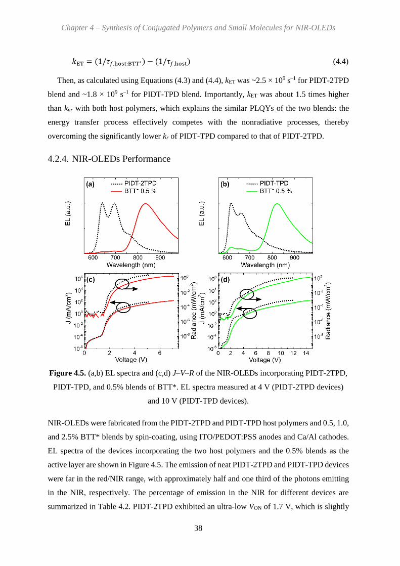
4.2.4. NIR-OLEDs Performance ................................................................................ 38
5. Synthesis of Conjugated Polymers for NIR-LECs ..................................................... 41
5.1. IDTT-Based Copolymer as the Single Emitter ........................................................ 41
5.1.1. Background and Motivation ............................................................................. 41
Page 14
xiv
5.1.2. Polymer Design, Synthesis, and Characterization ........................................... 42
5.1.3. Performance of the NIR-LECs ......................................................................... 46
5.2. Random Copolymers Incorporating D–A–D Segments as the Emitter ................... 49
5.2.1. Design of the Random Copolymers ................................................................. 49
5.2.2. Material Synthesis and Characterization .......................................................... 49
5.2.3. Performance of the NIR-LECs ......................................................................... 53
6. Application of Conjugated Polymers for OPDs ......................................................... 57
6.1. High-Speed OPDs Based on PIDT-TPD Donor Polymer ....................................... 57
6.1.1. Aim at High Performance ................................................................................ 57
6.1.2. Characterization of the PIDT-TPD/PCBM Blend ............................................ 58
6.1.3. Performance of the OPDs ................................................................................. 60
6.2. PIDT-2TPD as the Acceptor for All-PPDs .............................................................. 63
6.2.1. The D–A–A Design Motif ................................................................................ 63
6.2.2. Characterization of the P3HT/PIDT-2TPD Blend ........................................... 64
6.2.3. Performance of the All-PPDs ........................................................................... 66
7. Conclusion and Outlook ............................................................................................... 69
8. Methods .......................................................................................................................... 73
8.1. Stille Coupling ......................................................................................................... 73
8.2. Direct Arylation ....................................................................................................... 75
8.3. DFT Calculation ...................................................................................................... 76
8.4. AFM and TEM ........................................................................................................ 77
Acknowledgements ............................................................................................................... 79
Bibliography ......................................................................................................................... 81
Appendix ............................................................................................................................... 95
Page 15
Chapter 1 – Introduction
1
1. Introduction
What makes organic optoelectronics interesting is that they can be fabricated on flexible and
stretchable plastic substrates,[1-3] or even on transparent cellulose paper,[4-6] using solution-
based methods. This is relevant for wearable, implantable, and in vivo medical applications,
such as light-mediated sensing of heart and respiration rate, blood pressure, glucose level, and
oxygenation.[7-9] Organic semiconductors benefit from being mechanically conformable, like
many plastics, but they are also soluble and this can be exploited in the slot-die coating, inkjet,
or 3D printing of optoelectronics, which are thin, light-weight, and semi/fully transparent.[10-
14] Scalable low-cost processing of such devices in multiple shapes and sizes from nanometer
scale up to large-area screens and displays is attractive for a wide range of applications, some
of which are introduced in the following section.
1.1. Optoelectronics, a History Perspective
The story of electroluminescent diodes dates back to the 1960s and different GaP, GaAsP, and
GaAs semiconducting crystals, which were prepared at high temperatures, and which devices
were driven at extremely high current densities up to the order of 104 A/cm2.[15-19] This meant
that the lifetime of the diodes was short but, interestingly, they emitted light from the visible
to the near-infrared (NIR, defined as wavelengths λ >700 nm) spectral range. Thereafter, first
organic electroluminescent diodes were based on anthracene as a visible blue emitter,[20,21] and
in 1987 Tang and VanSlyke[22] reported a novel light-emitting device, which is now known as
an organic light-emitting diode (OLED). This early research has inspired the development of
highly sophisticated molecules that emit light in different colors over the visible spectrum, and
has enabled the commercialization of OLED displays, TV screens, and lighting applications.
However, the NIR range has remained far less developed among the organic emitters, and one
reason for that is the challenge for materials design set by the intrinsically decreasing emission
efficiency when moving from shorter to longer wavelengths, in other words, when redshifting
the emission. This issue will be discussed in more detail later in this thesis. The motivation for
the design of functional NIR emitters is that their applications can be extended from (night-
vision) displays to security,[23] light fidelity (Li-Fi) all-optical communication networks,[24-27]
photodynamic/photothermal therapy,[28-30] and biosensing.[31,32] The 650–950 nm range is of
particular interest for biomedical applications due to the semitransparency of skin and tissue
to the light at this spectral region.[33]
Page 16
Chapter 1 – Introduction
2
Figure 1.1. (a) Illustration of OLED device architecture. (b) Schematic energy diagram for
the injection and recombination of electrons (filled circles) and holes (empty circles). (c)
Photograph of a test device comprising eight OLEDs (showing the Al top contacts), as
fabricated at the facilities of Prof. Cacialli at UCL. The inset in part c shows the emission
from one of the OLEDs, as photographed from the bottom of the device in dark.
In an OLED, electrons are injected from the cathode and holes are injected from the anode,
and the recombination and light emission occurs at the active layer, as illustrated in Figure 1.1.
In the literature, polymer-based OLEDs are often differentiated with the naming polymer light-
emitting diode (PLED), but since the general working mechanism is the same in both devices,
they are simply referred to as OLEDs in this thesis. A typical OLED device is fabricated on a
transparent substrate, which is either glass or plastic, comprising indium tin oxide (ITO) as the
anode and poly(3,4-ethylenedioxythiophene):poly(styrenesulfonate) (PEDOT:PSS) as the
hole injection layer. Ca/Al are deposited on top of the active layer as the cathode. Additional
electron and hole blocking layers can be used to balance the charge transport in the device and
thereby improve the charge recombination efficiency in the active layer.[34-37]
In 1995, Heeger et al.[38-40] included an additional electrolyte salt in a polymer-based active
layer in a device called light-emitting electrochemical cell (LEC). Since then, LECs have been
under constant development to obtain good long-term stability,[41-45] which has become a key
feature that distinguishes LECs from other light-emitting devices. An LEC differs from OLED
in that the electrolyte forms a p–n junction doping structure upon turning on the device, that
is, in the electric field the cationic species drift toward the cathode forming a n-type doped
region and the anionic species drift toward the anode forming a p-type doped region. The p–n
junction contains the undoped electron–hole recombination zone, which is ideally formed in
the middle of the active layer (Figure 1.2).[46,47] In a well-functioning LEC, the p–n junction
ensures an efficient charge recombination without additional interlayers or low-work function
Page 17
Chapter 1 – Introduction
3
cathode metals, but the electrochemical stability of the active layer material plays an important
role in the device performance, as discussed later in this thesis.
Figure 1.2. (a) LEC device architecture. (b,c) Schematic representation of the formation of
the p–n junction doping structure during the initial turn-on process, and schematic energy
level diagram illustrating the injection of electrons (filled circles) and holes (empty circles)
through the energy barriers of the n-type doped (yellow) and p-type doped (white) regions.
The evolution of photoresponse devices is connected to the electroluminescent devices, and
the early versions of photodetectors were based on similar Ga, Ge, and Si semiconductors.[48-
51] The devices converted incident light into free charge carriers under an external reverse bias
voltage, and thus the photocurrent was strongly dependent on the electric field. Introduction
of the concept of heterojunction, based on two semiconductor materials (Ge/GaAs, Si/GaP,
GaAs/SiOx, etc.) in a crystalline double-layer, allowed better control of the band structure and
thereby more efficient separation of charge carriers at the interface of the two materials.[52-54]
An organic-inorganic heterojunction,[55,56] and the development of modern bulk heterojunction
(BHJ), based on fully organic semiconducting electron donor and electron acceptor, increased
the interfacial area and charge separation efficiency in the photoactive layer,[57-59] as illustrated
in Figure 1.3. Performance of organic photodetectors (OPDs) will be discussed in more detail
later in this thesis. Although the charge separation was efficient at the BHJ donor–acceptor
interface, charge transport was somewhat limited compared to the above mentioned crystalline
semiconductors, mainly because of the disordered morphology of the BHJ. This issue has been
improved with a morphological control and a range of donor and acceptor materials available
today.[60-65] In the current view, one of the main advantages of OPDs is the possibility to tune
their spectral response with the chemical structure of the photoactive layer, and thereby target
different applications, such as visible light communication (VLC),[66] night vision,[67,68] photo
and video imaging,[69-71] and biosensing.[72,73]
Page 18
Chapter 1 – Introduction
4
Figure 1.3. Schematic representation of an OPD comprising (a) heterojunction and (b) bulk
heterojunction photoactive layer, and (c) the corresponding device operation at reverse bias:
formation of the electron–hole pair (black dashed circle) via incident light absorption at the
donor–acceptor interface (black wavy arrow) and separation of the electrons (filled circles)
and holes (empty circles) into free charge carriers.
1.2. Design Considerations, Aim and Outline of the Thesis
Given the strong motivation for the use of solution-processable active layer materials in the
optoelectronic devices, this thesis focuses solely on the synthesis of conjugated polymers and
small molecules and their application for NIR-OLEDs, NIR-LECs, and OPDs for visible (red)
detection. For NIR-OLEDs, the general approach is to use a wide energy gap polymer as the
host matrix and a low energy gap molecule as the NIR emitter, which is either blended with
the polymer or incorporated into the polymer backbone. Both approaches are to aim at high
emission efficiency. However, the commercial polymer matrices are usually not ideal for NIR-
OLEDs because of the mismatch of their energy levels and poor spectral overlap with the NIR
molecules. The former is important for charge trapping at the NIR emitting sites and exciton
formation specifically at their locations, whereas the latter is related to the efficiency of energy
transfer from the host polymer to the NIR emitter. An interplay of these two mechanisms is
ultimately connected to the NIR emission efficiency. For a functional NIR-OLED, one needs
a host polymer that exhibits (i) good charge transport properties for low-voltage operation, (ii)
suitable frontier orbital energy levels for charge injection selectively at the NIR molecule, (iii)
high fluorescence efficiency, also in the solid state, and (iv) emission wavelength that overlaps
with the absorption of the NIR molecule to facilitate an efficient energy transfer. With these
criteria in hand, the remaining questions are:
What is the most feasible approach to mix the NIR emitter into the polymer matrix,
that is, by blending or copolymerization?
Page 19
Chapter 1 – Introduction
5
How much does the selection of host polymer impact the NIR performance, and are
there true alternatives for the well-known commercial polymer matrices?
For the application of polymeric NIR emitters for LECs, it is of great importance to study
if conjugated polymers can improve the commonly poor NIR-LEC performance via (i) good
electrochemical stability, (ii) balanced electrochemical p-type and n-typed doping capacities
and (iii) compatibility with the electrolyte salt for a well-behaving p–n junction formation, and
(iv) good long-term device stability, also in ambient air. Thus, two questions arise:
Can the NIR light-intensity be improved with the polymer approach, in comparison to
the previously reported materials, by fulfilling the above form-factor requirements?
What is the optimal type of polymer emitter, that is, should the active layer consist of
a single NIR-emissive polymer or can the inclusion of a wide-gap host and a low-gap
NIR emitter deliver better performance in the strongly doped driving conditions?
The applications of emissive polymers are not limited to light-emitting devices but they can
be also useful for light-harvesting applications, such as OPDs in this thesis. Well-functioning
polymer emitters commonly exhibit good electron- or hole-dominated mobilities or ambipolar
charge transport properties. Therefore, they can be used either as electron donor or electron
acceptor materials in a conversion of light into electrons and holes in the BHJ, and extraction
of the charge carriers in an electric field. Considering applications for example in imaging and
light communication, an OPD should ideally deliver a low dark current, high detectivity, and
high frequency response, in other words, detect light from the noise even at low intensities and
simultaneously operate at high speeds. A question arises:
What type of emissive polymer can be used as an active material to fulfill the OPD
device requirements – is an efficient emitter also a strong absorber?
The general considerations for the materials design and synthesis in this thesis are covered
in Chapter 2. The same chapter also introduces the critical characteristics that are studied and
optimized for the materials. These are the energy, wavelength, and efficiency of the absorption
and emission processes, the reversibility and stability of the electrochemical oxidation (p-type
doping) and reduction (n-type doping) processes, and the frontier orbital energy levels. The
different device parameters are introduced in Chapter 3, in consideration of the requirements
from a materials design perspective. Chapter 4 brings the preceding chapters into the context
of NIR emitters and summarizes the study on NIR-OLEDs and how the device performance
Page 20
Chapter 1 – Introduction
6
can be improved significantly with materials design, covering papers I and II. Introduction of
polymeric NIR emitters for LEC devices in Chapter 5 improves the general understanding of
electrochemical doping in the active layer, ultimately resulting in an intense NIR emission,
covering papers III and IV. Chapter 6 demonstrates that light-emitting polymers can be used
for the fabrication of highly functional OPDs, whose performance is comparable to that of the
conventional inorganic photodetectors. The efficiency of charge carrier separation and charge
extraction both play an important role in the device performance. These processes are studied
with polymer design and morphological control, covering papers V and VI. Overall, solution-
processing allows relatively easy and low-cost device fabrication procedure, but poses special
requirements for the materials design, both physical and mechanical, which are discussed and
effectively fulfilled in this thesis.
Page 21
Chapter 2 – Conjugated Materials and Optoelectronic Properties
7
2. Conjugated Materials and Optoelectronic Properties
This chapter gives a brief overview of different types of conjugated molecules, their structural
design, electrochemical properties, and light absorption and emission characteristics. These
properties are relevant in that they can be tuned with changes in the chemical structure, thereby
defining the performance of the materials in different electronic and photonic applications.
2.1. Definition and Design of Conjugated Molecules
Scheme 2.1. Chemical and resonance structures of different types of conjugated polymers.
As studied in organic chemistry, in a molecule with at least two adjacent sp2 hybridized carbon
atoms the sp2 hybrid orbitals form a single (σ) bond, whereas the overlap of the non-hybrid p-
orbitals contribute to a double (π) bond between the carbon atoms.[74] In an extended molecular
structure, the double bond electrons can diffuse (delocalize) along the neighboring p-orbitals,
which is referred to as a conjugated system. Scheme 2.1 shows a simple conjugated polymer
structure, a polyene, which consists of an undefined number of alternating single bonds and
double bonds. Since the π-electrons are shared along the entire polymer backbone, the double
bonds can “flip” freely between the carbon atoms, and this is drawn as a resonance between
the two structures. Both of these mesomeric forms are energetically identical.[75] The polymer
can also consist of a series of cyclic conjugated (aromatic) carbon rings, or other than carbon
atoms containing heteroaromatic structures, such as the sulfur atom containing thiophenes in
poly(thiophene). The thiophene rings are connected by σ-bonds to obey the rule of alternating
double bonds. Different from the planar and rigid π-bonds, the σ-bonds can rotate freely along
their axis. This allows certain freedom for the polymer backbone to twist between the repeating
thiophene units. In the case of poly(thiophene), the resonance results in the double bonds being
flipped between the thiophenes, known as a quinoid structure, which restricts the molecular
Page 22
Chapter 2 – Conjugated Materials and Optoelectronic Properties
8
motion and planarizes the polymer backbone.[76,77] This added stability means that the two
resonance structures (aromatic and quinoid) are no longer energetically comparable.
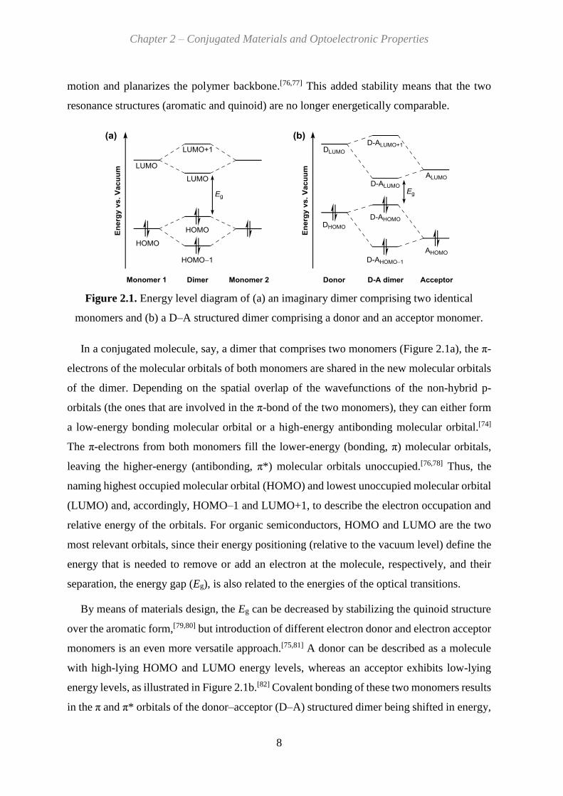
Figure 2.1. Energy level diagram of (a) an imaginary dimer comprising two identical
monomers and (b) a D–A structured dimer comprising a donor and an acceptor monomer.
In a conjugated molecule, say, a dimer that comprises two monomers (Figure 2.1a), the π-
electrons of the molecular orbitals of both monomers are shared in the new molecular orbitals
of the dimer. Depending on the spatial overlap of the wavefunctions of the non-hybrid p-
orbitals (the ones that are involved in the π-bond of the two monomers), they can either form
a low-energy bonding molecular orbital or a high-energy antibonding molecular orbital.[74]
The π-electrons from both monomers fill the lower-energy (bonding, π) molecular orbitals,
leaving the higher-energy (antibonding, π*) molecular orbitals unoccupied.[76,78] Thus, the
naming highest occupied molecular orbital (HOMO) and lowest unoccupied molecular orbital
(LUMO) and, accordingly, HOMO–1 and LUMO+1, to describe the electron occupation and
relative energy of the orbitals. For organic semiconductors, HOMO and LUMO are the two
most relevant orbitals, since their energy positioning (relative to the vacuum level) define the
energy that is needed to remove or add an electron at the molecule, respectively, and their
separation, the energy gap (Eg), is also related to the energies of the optical transitions.
By means of materials design, the Eg can be decreased by stabilizing the quinoid structure
over the aromatic form,[79,80] but introduction of different electron donor and electron acceptor
monomers is an even more versatile approach.[75,81] A donor can be described as a molecule
with high-lying HOMO and LUMO energy levels, whereas an acceptor exhibits low-lying
energy levels, as illustrated in Figure 2.1b.[82] Covalent bonding of these two monomers results
in the π and π* orbitals of the donor–acceptor (D–A) structured dimer being shifted in energy,
Page 23
Chapter 2 – Conjugated Materials and Optoelectronic Properties
9
given the contribution from two differential monomers. Importantly, the selection of the donor
and acceptor (and their corresponding energy levels) determine the HOMO and LUMO levels
of the D–A dimer, effectively decreasing its Eg in comparison to the example in Figure 2.1a.
The D–A approach[83] and its multiple variations, such as D–A–A, D–A1–D–A2, D–A–D, A–
D–A, and so on,[84-89] allow almost unlimited possibilities not only for the tuning of the HOMO
and LUMO and the Eg values, but also for changing the electrochemical and optical properties
of the molecule. The conjugation length is another factor that affects the orbital energies. The
Eg can be systematically decreased by extending the conjugation, that is, by adding more of
the energetically split π and π* orbitals, which result in the HOMO and LUMO approaching
each other.[90] Although this is effective only to a certain extent,[91-93] the Eg is usually smaller
for polymers than for similarly structured small molecules (monomers, dimers, etc.).[94-97]
2.2. Electrochemical Characterization
Figure 2.2. Schematic representation of (a) the fundamental energy levels, and (b) the
electrochemically and (c) optically accessible energy levels of an imaginary molecule.
The IUPAC definition for Eg is “the energy difference between the bottom of the conduction
band and the top of the valence band in a semiconductor”,[98] which describes the conventional
inorganic semiconductor crystals. In the case of conjugated molecules, this can be rephrased
as the difference in energy needed to remove an electron from the HOMO in gas phase, the
vertical ionization potential (IP), and the energy gained by adding an electron to the LUMO
in gas phase, the vertical electron affinity (EA).[99,100] These transitions are illustrated in Figure
2.2a. The fundamental energy gap (Efund) between the IP and EA can be estimated via density-
functional theory (DFT) calculations,[101,102] albeit with a great deal of approximations,[103-106]
or measured experimentally with ultraviolet photoelectron spectroscopy (UPS) and inverse
photoemission spectroscopy (IPES) techniques.[107-109] However, in the solid state, which is
Page 24
Chapter 2 – Conjugated Materials and Optoelectronic Properties
10
the state of interest for organic semiconductors, differential molecular orientations (disorder)
and intermolecular interactions (π–π stacking and polarization)[100] both influence the overall
energy structure of the material. Therefore, the measured values (in the solid state) may be
considerably different from the Efund.
Max
EndIncre
asin
g P
ote
ntial
Time
Start
(a)
(b) Min
EndStart
Incre
asin
g P
ote
ntial
Time
Figure 2.3. Linear (a) forward and (b) reverse potential scans. (c) CV traces of a reversible
Fc/Fc+ redox couple (black line), a quasi-reversible polymer (red line), and an irreversible
polymer (blue line), all at a scan rate of 100 mV/s. Determination of the oxidation (Eox) and
reduction (Ered) onset potentials, the anodic (Epa) and cathodic (Ep
c) peak potentials, and the
anodic (ipa) and cathodic (ip
c) peak currents. The arrows indicate the scan direction.
Cyclic voltammetry (CV) is a practical method for the estimation of the HOMO and LUMO
energy levels via electrochemical doping, that is, by removing an electron from the molecule
(oxidation, p-type doping) or by adding an electron to the molecule (reduction, n-type doping),
respectively.[110-112] These electron transfer reactions can be studied by depositing the material
on a working electrode surface as a solid-state thin film, and then immersing it in a supporting
electrolyte solution (or alternatively dissolving the material in the electrolyte solution). A 0.1
M solution of tetrabutylammonium hexafluorophosphate (TBAPF6) in anhydrous acetonitrile
is a commonly used electrolyte.[113] Conveniently, polar acetonitrile does not usually dissolve
the films of conjugated polymers and small molecules. The CV data is collected by applying
a positive (forward, Figure 2.3a) or negative (reverse, Figure 2.3b) linear potential scan to the
electrode. At a certain pre-set voltage, the scan is switched to an opposite direction at the same
-2.0 -1.5 -1.0 -0.5 0.0 0.5 1.0
Eox
Eox
Ered
Ecp
Ecp
Eap
Eap
Ecp
Eap
icpC
urr
en
t (A
)
Potential vs. Fc/Fc+ (V)
(c) iap
Page 25
Chapter 2 – Conjugated Materials and Optoelectronic Properties
11
scan rate. An anodic wave appears upon oxidation of the material on the forward scan, and a
cathodic wave appears during the reverse scan, as illustrated in Figure 2.3c.[114]
For a redox couple exhibiting fast single electron transfer, referred to as a reversible couple
(Figure 2.3c, black line), (i) separation of the anodic (Epa) and cathodic (Ep
c) peak potentials,
i.e., ΔEp = |Epa – Ep
c|, is 57 mV, (ii) the anodic (ipa) and cathodic (ip
c) peak currents are
approximately the same, thus |ipa/ip
c| = 1, (iii) the position of the peak potentials (Epa, Ep
c)
remain constant regardless the scan rate, but (iv) the peak currents (ipa, ip
c) are proportional to
the square root of the scan rate,[115] i.e., they increase with increasing scan rate.[114,116] For a
quasi-reversible electrochemical reaction (Figure 2.3c, red line), the oxidation and reduction
are still relatively fast, but a certain energy barrier for the electron transfer requires a higher
applied potential for the oxidation/reduction to occur. Therefore, the value of ΔEp becomes
larger than 57 mV, changing as a function of the scan rate, and the peak currents are no longer
proportional to the square root of the scan rate. For a slow or unstable electrochemical reaction,
referred to as an irreversible redox couple (Figure 2.3c, blue line), CV trace lacks the reverse
reaction completely (that is, during the scan at the opposite direction of the forward or reverse
scan).[117] Chemical reversibility refers to stability of the material during oxidation/reduction,
and whether or not it can be re-reduced/re-oxidized.[118]
It is important to note that the oxidation and reduction of a conjugated polymer (or small
molecule) at the electrode surface leads to conformational reorganization,[112] such as changes
between the aromatic and quinoid resonance structures.[80] Therefore, the redox properties are
characterized from the oxidation (Eox) and reduction (Ered) onset potentials (see Figure 2.3c).
Eox describes the lowest energy needed to remove an electron from the HOMO,[119] and Ered
refers to the energy of adding an electron to the LUMO,[120] which are observed as increasing
anodic and cathodic currents in the CV traces, respectively. The HOMO and LUMO can be
assessed by measuring the onset potentials. However, the CV method does not provide direct
indication of their energy in the vacuum scale (as in the case of IP and EA). It necessitates the
use of a reference redox couple with a known, standard potential. [Fe(Cp)2]/[Fe(Cp)2]+ couple,
known as ferrocene/ferrocenium (Fc/Fc+) couple, is a common standard with a redox potential
of 0.63 V against the normal hydrogen electrode (NHE) in acetonitrile at 25 °C,[121] and the
NHE in turn has an electrode potential of –4.5 V in the vacuum scale.[115] This allows an
indirect evaluation of the HOMO and LUMO energies by measuring the Eox and Ered versus
the Fc/Fc+ redox couple at 0 V, respectively, and by using the following equations:
Page 26
Chapter 2 – Conjugated Materials and Optoelectronic Properties
12
𝐸HOMO = −(𝐸ox + 5.13) (eV) (2.1)
𝐸LUMO = −(𝐸red + 5.13) (eV) (2.2)
With these approximations, it is evident that the electrochemically accessible values of the
HOMO and LUMO energies in the vacuum scale, or the Eg, are not directly comparable to the
fundamental IP and EA in the gas phase, nor to the Efund. However, they do give an excellent
indication of the p-type and n-type doping processes (i.e., hole and electron injection), their
energies, and the electrochemical reversibility and stability, which are highly relevant for the
performance of the materials in the optoelectronic devices.
2.3. Characterization of the Light Absorption and Emission
The characterization techniques in the previous section did not take into account the electron–
hole pair binding energy (EB).[122] Upon absorption of a photon (i.e., excitation) an electron–
hole pair (i.e., exciton) is formed. EB describes the additional energy required to overcome the
attractive Coulomb force and dissociate the electron and hole into free charge carriers.[123,124]
Thus, the lowest accessible vertical excitation, the optical energy gap (Eopt), is generally lower
than the electrochemically measured Eg (or the Efund), as schematically illustrated in Figure
2.2c.[100,125] Eopt is obtained experimentally from the low-energy absorption onset (λonset) of the
material, either in solution or solid-state thin film, given the Planck relation:[126]
𝐸opt = ℎ𝜈 = ℎ𝑐/𝜆 ≈ 1240/𝜆onset (eV) (2.3)
where h is Planck constant (6.626 × 10⁻³⁴ J s, or 4.135 × 10⁻¹⁵ eV s),[127] ν is the frequency, c
is the speed of light in vacuum (2.998 × 10⁸ m/s), and λ is the wavelength. Estimation of λonset
in nanometers (10–9 m) thus relates to the Eopt in eV, as shown in Figure 2.4.[128] Interpretation
of the rest of the absorption spectrum is less straightforward. Where Eopt describes the vertical
excitation from the ground state (S0) to the lowest-energy singlet excited state (S1), the overall
absorption of conjugated molecules is a sum of transitions from the S0 state to the different
electrically and vibrationally excited (S1, S2, etc.) states.[74,126,129] This leads to a broadening
of the absorption band, as shown in Figure 2.4 and further schematically illustrated in Figure
2.5. The energy differences between the vibrational levels (Figure 2.5a, grey lines) are, in
general, smaller than those of the electronic levels (Figure 2.5a, black lines). Therefore, the
classical electronic transitions (S0 → S1, S0 → S2, etc.) require the high energy of UV-visible
Page 27
Chapter 2 – Conjugated Materials and Optoelectronic Properties
13
photons, or that of the injected electrons, while the vibrational transitions can be induced with
low-energy infrared, or even NIR photons.[74]
400 450 500 550 600 650 700 750 800
Inte
nsity
Wavelength (nm)
onset
Absorption Fluorescence
Figure 2.4. Absorption and PL spectra of an imaginary conjugated polymer.
Absorption of light by the molecule can be assessed with Lambert–Beer law, which states
that the light passing through the sample is diminished by three physical factors: (i) the amount
of absorbing material that the light must travel through, i.e., its concentration, (ii) the distance
the light must travel through the sample, i.e., the path length, and (iii) the probability that the
photon of a given energy is absorbed, i.e., the absorption coefficient of the sample. Then, if an
incident light of an intensity of I0 passes through the sample, a certain (lower) intensity of It is
transmitted through. The law assumes that the proportion of light absorbed by the molecule is
independent of the magnitude of I0. Thus, if the sample (solution or thin film) is homogeneous,
the probability of light absorption is linearly dependent on the intensity, and each successive
layer of the sample absorbs an equal fraction of light across a finite length scale. This means
that the magnitude of It decreases exponentially with increasing path length, or with increasing
concentration (for solution). The relation of I0 to It is defined as absorbance (Abs, or Aλ):[74,126]
𝐴𝜆 = log (𝐼0/𝐼𝑡) = 𝜀 𝑐 𝑙 (2.4)
where ε is the molar absorptivity (i.e., extinction coefficient) with units M–1 cm–1 (or L g–1 cm–
1), c is the solution concentration in M (or g/L), and l is the path length in centimeters. The
constant ε depends on the material, describing its ability to absorb light. The absorption spectra
of conjugated molecules are usually measured over a wavelength range, as in Figure 2.4, either
in a solution of low concentration (in a quartz cuvette with 1 cm path length) or as a thin film
with thickness of ~100 nm.[130-132] In the latter case, Equation (2.4) becomes:[133]
𝐴𝜆 = 𝛼 𝑙 (2.5)
Page 28
Chapter 2 – Conjugated Materials and Optoelectronic Properties
14
where α describes the absorption coefficient of the material in thin film, with a unit cm–1, and
l is the film thickness (i.e., path length) in centimeters. The absolute value of α (or ε) depends
strongly on the wavelength, and is therefore reported as a plot versus wavelength, or as a value
connected to a specific wavelength (typically that of the absorption peak maximum).
Figure 2.5. Jablonski diagram of an imaginary molecule, illustrating the low-lying energy
levels involved in the excitation of an electron via absorption of a photon, some nonradiative
relaxation pathways (black arrows), and radiative relaxation as (a) fluorescence, (b)
phosphorescence, and (c) thermally activated delayed fluorescence.
Fluorescence spectroscopy measures the emitted photons in relation to the absorbed ones,
which emission is generally referred to as photoluminescence (PL). Conjugated molecules can
exploit the energy of excited electrons as radiative relaxation back to the S0 state (apart from
the specific case of exciton dissociation in the BHJ, see Chapter 1). Figure 2.5a represents a
conjugated molecule, whose S0 state electron is optically excited to the low-energy Sn (where
n = 1, 2, etc.) electronic state or vibronic state. Countless possibilities of internal conversion
(IC) and vibrational relaxation (VR) to the lower energy levels ultimately lead to a relaxation
from the S1 state to different electronic and vibronic S0 state energy levels. The latter process
is termed fluorescence. Similarly to the absorption process discussed above, the combination
of different energy transitions to the S0 state leads to a broadening of the emission band (see
Figure 2.4). Various nonradiative decay processes can take place, such as vibronic coupling
of the S0 and S1 states, as schematically illustrated on the left side of Figure 2.5a, or intersystem
crossing (ISC) to a lower-lying triplet excited (Tn) state and further nonradiative relaxation to
the S0 state (not included in Figure 2.5a). These undesired transitions decrease the fluorescence
efficiency, which is defined as photoluminescence quantum yield (PLQY, or Φf):[126,129,134]
Page 29
Chapter 2 – Conjugated Materials and Optoelectronic Properties
15
𝛷𝑓 = 𝑘𝑟/(𝑘𝑟 + 𝑘𝑛𝑟) = 𝑁emitted/𝑁absorbed (2.6)
where the kr is the radiative rate constant, and knr is the nonradiative rate constant describing
the above mentioned dark decay processes. Φf can be obtained experimentally by measuring
the relative number of the absorbed and emitted photons, Nabsorbed and Nemitted, respectively, in
comparison to a dye with a known, standard Φf,[135] while the absolute values of Nabsorbed and
Nemitted can be measured with an integrating sphere.[136,137] The latter method is desired due to
its accuracy and applicability for both solution and thin film samples.
The average time a molecule remains excited before spontaneous emission via relaxation
from the S1 state to the S0 state is termed fluorescence lifetime (τf):[129]
𝜏𝑓 = 1/(𝑘𝑟 + 𝑘𝑛𝑟) (2.7)
which is typically in the order of 10–9 s for fluorescent molecules (for comparison, Sn → S1 IC
and VR processes are even faster, in the order of 10–10–10–14 s).[126,134] τf can be measured
experimentally with a time-correlated single-photon counting (TCSPC) technique.[138] Thus,
kr and knr can be derived from Equations (2.6) and (2.7) as following:
𝑘𝑟 = 𝛷𝑓 (𝑘𝑟 + 𝑘𝑛𝑟) = 𝛷𝑓 (1/𝜏𝑓) = 𝛷𝑓/𝜏𝑓 (2.8)
𝑘𝑛𝑟 = 1/𝜏𝑓 − 𝑘𝑟 (2.9)
which allows a direct evaluation of the two competing processes in a fluorophore.
In further discussion of optical excitation and emission processes, it is worth taking a closer
look into the electronic spin states. An electron can be described as having an intrinsic angular
momentum, a spin quantum number of s = 1/2, with the notion that it does not behave like a
negatively charged particle rotating around its axis. Instead, the alignment of the spin (a vector
along a reference direction, an arbitrarily chosen axis) is identified as a spin magnetic quantum
number ms = +1/2 or –1/2.[74,139] These two possible values of ms are commonly represented
as spin-up, or ↑, and spin-down, or ↓, respectively, as for example in Figure 2.1. If there are
multiple electrons to be taken into account, the total spin angular momentum quantum number
(the resultant spin) is given by S = s1 + s2, s1 + s2 – 1, …, |s1 – s2|, where si is the spin of ith
electron. Considering two coupled electrons in a molecule, S can be either 1 or 0, and there
are four possibilities for the arrangement of their spin configurations, given by the multiplicity
M = 2S + 1, one corresponding to singlet state (M = 1) and three corresponding to triplet state
(M = 3).[139,140] In fact, multiplicity tells the number of allowed values of the total spin
Page 30
Chapter 2 – Conjugated Materials and Optoelectronic Properties
16
magnetic quantum number Ms = S, S – 1, …, –S for a given value of S, in other words, the
possible orientations (spin vectors in space) that the total spin can adopt.[74,101,139]
Figure 2.6. Schematic representation of the electron spin (ms = ±1/2ħ). Individual electron
spins are shown as vectors (blue arrows) lying in cones along the z-axis and the total spin is
shown as a vector (red arrow) lying between two coupled electrons. (a) A singlet has zero
total spin angular momentum (S = 0): whenever one spin vector lies on its cone, the other
points to an opposite direction, cancelling the overall spin. (b) A triplet has three ways of
achieving a nonzero total spin angular momentum (S = 1): the spin vectors lie either in the
same cone (Ms = ±1ħ) or in opposite cones but in phase (Ms = 0 along the z-axis).
In Figure 2.6, the individual spins ms and their resultant Ms are shown as vectors precessing
about an arbitrarily chosen z-axis. In the case of S = 0, M = 1, there is only one possible spin
orientation, Ms = 0, thus the naming singlet: the electron spins are paired (opposite/antiparallel)
and there are no net spin. When S = 1, M = 3, there are three possible spin orientations, Ms =
+1, 0, or –1, and thus the naming triplet: the two electrons are unpaired (parallel/in phase) and
the net spin S = 1 in all cases.[74,101,139]
The above description gives an intrinsic singlet–triplet exciton formation ratio (ηST), often
termed “spin statistics”,[74,141,142] since the same spin vectors apply to the excited states.[140,143]
However, virtually all conjugated molecules exhibit a singlet ground state configuration, i.e.,
all electrons are paired, and absorption of a photon results in excitation from the S0 state to the
corresponding Sn state with no change in the electron spin.[74,139] This is known as spin-allowed
transition. The ISC process allows the occupation of the triplet excited Tn states, and ultimately
the fraction of excitons located at the singlet state is 25%, while 75% of the excitons are formed
as triplets. Relaxation from excited T1 state to S0 ground state requires the spin of the electron
Page 31
Chapter 2 – Conjugated Materials and Optoelectronic Properties
17
to flip or rephase, and is therefore spin-forbidden.[74,139] Moreover, kr for the T1 → S0 transition
is relatively low, in the order of 101–103 s–1, whereas knr for the triplet exciton is significantly
higher, typically in the range of 105–106 s–1.[126,144-146] This means that the nonradiative decay
dominates the triplet state, i.e., the triplet excitons are dark, thereby intrinsically limiting the
emission of the fluorescent molecules to the radiative S1 → S0 transition. Despite the fact that
ηST is given by default, a low knr (via assumed, slow S1 → S0 IC and Sn → Tn ISC processes)
and a high kr (via fast, radiative S1 → S0 relaxation) can improve the PLQY of a fluorescent
dye up to 100%.[147,148] This and many additional factors, such as (i) backbone planarity and
rigidity in connection to vibrational and rotational energy losses, (ii) π–π interactions and
aggregation, and (iii) spatial overlap between the S1 state electron and hole wavefunctions
ultimately define the emission properties, as discussed in the later chapters.
Introduction of a (heavy) transition metal to the conjugated structure induces strong spin–
orbit coupling between the singlet and triplet states, known as heavy atom effect, allowing a
fast Sn → Tn ISC process and spin-forbidden radiative relaxation from the T1 excited state to
the S0 ground state as phosphorescence.[144,145,149,150] This process is illustrated in Figure 2.5b.
Phosphorescent materials can utilize larger amount of excitons than the fluorescent ones, but
kr for T1 → S0 transition is still somewhat lower than that for the S1 → S0 transition due to the
spin flip necessary in the former case.[126] The low decay rate of phosphorescent emitters may
result in exciton quenching, saturation, and triplet–triplet annihilation, which are detrimental
to the performance of light-emitting devices.[150-152] However, different Pt and Ir complexes
have been reported to exhibit kr up to the order of 106 s–1 or even higher, which importantly
exceed the typical knr of triplet excitons.[153-158]
The singlet–triplet energy gap (ΔEST) can be substantially large if the ground state HOMO
and LUMO wavefunctions overlap, e.g., in a nearly coplanar D–A–D structured molecule, as
the electron configuration is generally maintained at the excited states, referred to as locally
excited states (LE). This is often the case in highly fluorescent molecules. In contrast, spatial
separation of the HOMO and LUMO wavefunctions by the design of orthogonal donor and
acceptor units leads to charge-transfer excitation (CT) character and small ΔEST.[159,160] The
latter has been used for the transfer of dark triplet excitons back to the radiative singlet state
via reverse intersystem crossing (RISC), ultimately for the attainment of emission as delayed
fluorescence. This emission mechanism is known as thermally activated delayed fluorescence
(TADF),[161-164] which name comes from the original understanding that the RISC process is
Page 32
Chapter 2 – Conjugated Materials and Optoelectronic Properties
18
mediated by thermal energy to raise the triplet excitons to a vibrational level that corresponds
energetically to the singlet state, as presented in Figure 2.5c. However, thermal energy and the
simplified Jablonski diagram do not provide full picture of the TADF mechanism. It involves
vibronic coupling between the lowest local excitation triplet state (3LE) and the lowest charge-
transfer triplet state (3CT) to promote spin–orbit coupling and spin flip to the lowest charge-
transfer singlet (1CT) state.[165-171] The key difference to the fluorescent (and phosphorescent)
molecules is that the TADF mechanism allows harvesting of up to 100% of the dark triplet
excitons as higher energy radiative singlet excitons, thereby surpassing the 25% singlet exciton
yield (and the 75% triplet exciton yield) without the inclusion of heavy metals.[172-174] TADF
emitters benefit from higher yield of emissive excitons than the fluorescent or phosphorescent
ones, but decay rate of the delayed fluorescence is somewhat lower than that of the fluorescent
ones due to the involvement of the long-lived triplet excitons. The rate of the RISC process
(kRISC) is critical for the TADF lifetime, and delayed fluorescence is generally attainable thanks
to the substantially higher kRISC (106–107 s–1 or even above) compared to the kr and knr of the
triplet states.[175]
All the three emission mechanisms described above (and shown in Figure 2.5) have their
specific challenges when Eg (and thereby Eopt) is decreased, due to vibronic coupling between
the ground state and the different excited states. Organic (metal-free) fluorescent emitters bear
some important benefits from an application point of view, which are discussed in detail in the
following chapters.
Page 33
Chapter 3 – Organic Optoelectronic Devices
19
3. Organic Optoelectronic Devices
This chapter describes the application of conjugated materials as semiconductors for different
optoelectronic devices: organic light-emitting diodes, light-emitting electrochemical cells, and
organic photodetectors. The parameters that define the device performance are discussed with
some key considerations, keeping in mind that the design of materials for these applications
are discussed in depth in the later chapters.
3.1. Organic Light-Emitting Diodes
The positioning of HOMO and LUMO levels of the active material define the recombination
site of the injected holes and electrons, and the concomitant generation of radiative photons as
electroluminescence (EL), as schematically represented in Figure 1.1 (Chapter 1).[176-178] The
overall efficiency of this process can be characterized as an external quantum efficiency (EQE,
or ηExt) of the OLED, that is, the number of emitted photons (Nph,out) divided by the number of
injected charges (Nel,in):[150,179]
𝜂Ext = 𝑁ph,out/𝑁el,in = 𝛷𝑓 × 𝜂ST × 𝜂Rec × 𝜂Out = 𝜂Int × 𝜂Out (3.1)
where Φf is the PLQY of the emitter, given by Equation (2.6), and ηST = 0.25 for fluorescent
emitters, which obey the same spin selection rule as discussed in the case of optical excitation
in Chapter 2.3. The key difference between optical and electrical excitation is, however, that
in the latter case both singlet excitons and dark triplet excitons can be formed directly at the
electron and hole captures.[141,143,145] ηRec is the charge balance factor, i.e., exciton formation
efficiency. It describes the fraction of recombining charge carriers relative to the total number
of injected carriers. In an ideal case, all injected electrons and holes recombine and ηRec = 1.
However, the charge balance depends strongly on the current density, and imbalanced charge
transport and saturation of the emissive sites at high currents can decrease ηRec << 1. A low
decay rate of the emitter is disadvantageous for the performance of the device, as the emitter
is saturated already at low current densities. This is observed as EQE roll-off when the current
density is increased, thus strongly limiting the device operation.[150,180-183] The high decay rates
of fluorescent emitters typically allow operation at relatively high currents with little EQE roll-
offs. The above three factors together describe the internal quantum efficiency (IQE, or ηInt)
of the device, which can be described as the number of generated photons (but not leaving the
device) per the number of injected charges.[150,179]
Page 34
Chapter 3 – Organic Optoelectronic Devices
20
The remaining factor, ηOut, is the optical outcoupling efficiency, i.e., the fraction of photons
passing through the substrate, anode, and possible interlayers relative to the photons generated
in the active layer. ηOut is typically ~0.2 due to waveguiding in the glass substrate and different
device layers and reflections at the interfaces.[184,185] Majority of the photons are either trapped
inside the substrate/device or emitted from the edges of the device.[37] In a fluorescent OLED,
the theoretical maximum EQE is therefore limited to ~5%.[179] As observed, ηOut is a significant
source of efficiency loss, and various engineering approaches have been applied to improve
the light outcoupling. This is usually done by minimizing the waveguiding effect with different
nanostructures,[186] microcavity structures,[187,188] and microlenses in the device,[189,190] which
extract the trapped light out of the device.[191,192]
Another way to characterize the OLED performance is the current efficiency (cd/A), which
represents the ratio of luminance to the applied current density. Luminous efficiency (lm/W)
describes the ratio of luminous flux to the electric power input. Both of these parameters take
into account the sensitivity of human eye to different wavelengths of visible light, known as
photopic response, with a maximum sensitivity at 555 nm.[150,178,179,193] The current efficiency
and the luminous efficiency are not ideal quantities for OLEDs emitting in the NIR region, for
which EQE is commonly used.[150] Moreover, since luminance (often referred to as brightness,
in cd/m2) is related to the photopic response and emission in the visible spectral range, radiance
(R, in mW/cm2) is more practical measure for the intensity of NIR emission.
A plot of current density and radiance versus voltage (J–V–R) is used for further evaluation
of the device performance: current density (J, in mA/cm2), i.e., the ratio of current to the area
of the device, and radiance are measured with respect to an increasing applied voltage (V, V).
Turn-on voltage (VON) describes the minimum voltage to turn on the device, that is, to reach
certain increase of radiance (or current) from the baseline.[37,89,194]
3.2. Light-Emitting Electrochemical Cells
The performance of LECs is characterized largely with the same parameters as described for
OLEDs in the previous section. However, in an LEC the electrolyte ions form the p-type and
n-type doped regions in the active layer, and in these regions the electric field can be extremely
high.[195] This results in bending of the energy levels near the electrode/active layer interfaces,
as schematically illustrated in Figure 1.2 (Chapter 1). When the applied voltage is large enough
to overcome the energy barrier, injection of electrons and holes will take place. The p–n doping
Page 35
Chapter 3 – Organic Optoelectronic Devices
21
process can be described as the injected electrons being stabilized by uncompensated cationic
electrolyte species at the cathode side of the active layer and the injected holes being stabilized
by uncompensated anionic electrolyte species at the anode side, thus the naming n-type and p-
type doped regions, respectively.[195-197] Because of this stabilization, it is possible to inject a
large number of charge carriers into the active layer. The two doped regions grow in time and
eventually contain the electron–hole recombination zone, given that the doping is balanced, in
the middle of the active layer and far from the exciton quenching electrodes.[44,198-200]
When the LEC is driven with a constant current density, the formation of the p–n junction
doping structure is observed as increasing radiance (or luminance) and decreasing voltage with
time during the initial turn-on process. A well-functioning device thus reaches the steady-state
operation rapidly. The time to reach certain radiance is reported as the turn-on time.[201-203] At
the steady-state operation, the p–n junction ensures efficient recombination of electrons and
holes in the active layer, and ηRec = 1 also at high current densities.[46,204-206] The result may be
that the electrolyte ions separate completely at the electrode/active layer interface during the
continuous long-term operation, which deteriorates the p–n doping structure, and is observed
as decreasing radiance (or luminance).[43,206-209] One way to circumvent this is to apply a pulsed
or alternating current, which limits the motion of the electrolyte ions.[210,211] It is desirable that
the active layer itself ensures a stable p–n junction by containing the ions, through the design
of the active material and the electrolyte, and allows the operation also under constant current.
3.3. Organic Photodetectors
In an OPD, the photogenerated free charge carriers are driven to their respective electrodes by
the alignment of the HOMO and LUMO energy levels of the donor and acceptor materials (an
internal built-in potential) and even more by the external reverse bias, as represented in Figure
1.3 (Chapter 1).[59,212-214] EQE describes the fraction of the incident photons that contribute to
the photocurrent, which is measured as the number of photogenerated charges at the electrodes
(Nel,out) divided by the number of incident photons (Nph,in) at a given wavelength:
EQE = 𝑁el,out/𝑁ph,in (3.2)
Responsivity (R, in A/W) is a measure of sensitivity of an OPD to light (in the conversion
of optical power to electrical current), which can be characterized as the ratio of photocurrent
density under illumination (Jph, A/cm2) to the incident light intensity (LLight, W/cm2) as:[59,215]
Page 36
Chapter 3 – Organic Optoelectronic Devices
22
𝑅 = 𝐽ph/𝐿Light (3.3)
It may not be obvious from Equation (3.3) that responsivity varies with the wavelength of the
incident light. An alternative expression for responsivity can be derived from EQE as:[212,213]
𝑅 = EQE × 𝜆𝑞/ℎ𝑐 (3.4)
where λ is the wavelength, q is the elementary charge (1.602 × 10⁻¹⁹ C),[127] h is the Planck
constant (6.626 × 10⁻³⁴ J s), and c is the speed of light (2.998 × 10⁸ m/s). Equation (3.4) shows
how EQE relates to the responsivity. It is important to obtain high EQE for the attainment of
high responsivity. In general, the responsivity can be increased by ramping up the reverse bias,
since a higher electric field increases the charge collection efficiency.[61,215]
Noise equivalent power (NEP, W) is the minimum optical power that an OPD distinguishes
from the noise, that is, an incident light power that generates a photocurrent equal to the noise
current (in, in A):[59,215,216]
NEP = 𝑖n/𝑅 = √(𝐴𝛥𝑓)/𝐷* (3.5)
where A is the surface area of the device in cm2, Δf is the electrical bandwidth in Hz, and D*
is the specific detectivity in cm Hz1/2 W–1 (Jones).
On the other hand, specific detectivity describes the sensitivity of an OPD in relation to the
surface area, the frequency bandwidth, and the noise current, which can be described as:
𝐷* = √(𝐴𝛥𝑓)/NEP = 𝑅√(𝐴𝛥𝑓)/𝑖n (3.6)
The literature commonly describes three different sources of noise that contribute to in: (i) shot
noise (or dark current noise) due to statistical fluctuation of the current when operating in the
biased mode, (ii) Johnson noise (or thermal noise) due to random thermal motion of the charge
carriers, and (iii) Flicker noise, which is inversely proportional to the frequency, whereas the
other two are frequency independent.[59,212,213] In a typical OPD operation, under reverse bias,
the shot noise from dark current is assumed to have the dominant contribution.[13,72] Therefore,
in = (2qIdΔf)1/2 and D* can be calculated as following:[212-214,217]
𝐷* = 𝑅√𝐴/√(2𝑞𝐼d) = 𝑅/√(2𝑞𝐽d) (3.7)
where Id is the dark current in A and Jd is the dark current density in A/cm2. The latter form of
Equation (3.7) is convenient for the characterization of specific detectivity, since responsivity
can be obtained from EQE using Equation (3.4). Measurement of current density at increasing
Page 37
Chapter 3 – Organic Optoelectronic Devices
23
applied reverse bias (a J–V plot) in dark and under illumination reveal the values of Jd and Jph
at a chosen voltage, respectively. Equation (3.7) shows that D* is determined not only by the
responsivity (photocurrent) but also by the noise (dark current).[13,218] The BHJ should ideally
deliver as low Jd as possible, since it is a major limiting factor for the detectivity. Additional
electron and hole blocking layers can be used to increase the barrier for charge injection from
the anode and cathode, respectively, thereby reducing the dark current under reverse bias. The
thickness of the BHJ layer is another factor that affects the dark current. A thicker film usually
exhibits lower Jd, but the thickness also influences the EQE and the responsivity of the device,
often contrary to the desired change in dark current.[61,212,217,219-221]
Page 38
Chapter 3 – Organic Optoelectronic Devices
24
Page 39
Chapter 4 – Synthesis of Conjugated Polymers and Small Molecules for NIR-OLEDs
25
4. Synthesis of Conjugated Polymers and Small Molecules for NIR-
OLEDs
The major challenges in the design of efficient NIR emitters are (i) aggregation quenching of
the emission in solid state, (ii) pronounced coupling of the excited state and the ground state
vibronic energy levels toward decreasing energy gap, known as the “energy gap law”,[222,223]
and (iii) intrinsic limitation of the yield of emissive excitons from the singlet excited state. A
number of strategies have been introduced to overcome these challenges and to improve the
performance of organic (metal-free) compounds in the NIR range.[224,225] Aggregation-induced
emission (AIE) enhances the solid-state emission yield by restricting intramolecular motion
(rotation and/or vibration) of the emitter.[226-228] Ledwon et al.[229] reported a top-performing
AIE-active benzothiadiazole small molecule and an OLED emitting at 688 nm. TADF harvests
the commonly dark triplet excitons in organic compounds (Chapter 2.3).[164,168,230-234] In recent
years, examples of TADF emitters and various TADF-AIE hybrid systems have been reported
to exceed a peak wavelength of 700 nm and an EQE of ~10%.[235-241] In such triplet harvesting
compounds the exciton recombination dynamics typically fall in the hundreds of nanoseconds
or even in the microsecond range. This limits the operational bandwidth when integrated in
devices for telecommunication. Fluorescent polymers and small molecules are preferred for
Li-Fi applications,[24,26] since the fluorescence lifetime of these materials is typically in the
order of few nanoseconds or less, allowing data transmission rates up to Gb/s.
To redshift the emission of a fluorophore into the NIR region, one needs a planar structure
with strong electron donating and accepting moieties. Such planar structures benefit from the
concomitant extended conjugation and decreased energy gap but, at the same time, suffer from
strong intermolecular π–π stacking, which is known as aggregation. Therefore, the NIR emitter
is usually diluted in a solid-state polymer or small molecule matrix, referred to as a host/guest
system.[88,165,242] The host matrix should physically separate the emitters from each other to
avoid strong aggregation, yet allow efficient energy transfer and charge trapping at the NIR
emissive sites for an ideal OLED performance. In this chapter, two different approaches are
discussed with the aim of designing organic host and guest materials for an efficient NIR
emission, covering papers I and II.
Page 40
Chapter 4 – Synthesis of Conjugated Polymers and Small Molecules for NIR-OLEDs
26
4.1. Random Copolymers Comprising BTT as the Emitter
4.1.1. Design Strategy
Phase separation of the host matrix and the NIR emitter may become a significant problem in
the host/guest type OLEDs. Diluting the emitter within a host polymer backbone can be an
ideal way to obtain a solution-processable homogeneous blend and prevent the NIR molecules
forming phase separated aggregates.[194,243] The design of host polymer and guest emitter
generally requires (i) spectral overlap of the host emission and guest absorption to ensure
efficient energy transfer, (ii) careful optimization of the host and guest band alignment to allow
charge injection and trapping specifically at the NIR sites, and (iii) suitable energy levels with
regard to the electrodes and interlayer materials available for device fabrication. In this study,
two wide gap polymers were chosen as host matrices: poly[3,3'-ditetradecyl-2,2'-bithiophene-
5,5'-diyl-alt-5-(2-ethylhexyl)-4H-thieno[3,4-c]pyrrole-4,6(5H)-dione-1,3-diyl] (P2TTPD)
and poly[3,3'-ditetradecyl-2,2':5',2'':5'',2'''-quaterthiophene-5,5'''-diyl] (P4T). The amount of
NIR emitter is highly related to the performance of the OLEDs and the optimum concentration
needs to be studied for each new system. The low-gap NIR molecule 6-(2-butyloctyl)-4,8-
di(thiophen-2-yl)-[1,2,3]triazolo[4',5':4,5]benzo[1,2-c][1,2,5]thiadiazole (BTT, Scheme 4.1
and 4.2) was copolymerized into the host polymer backbone with the concentration varying
from 0.5 to 10%. In all cases, the NIR emitter was dispersed in the host polymer backbone,
allowing cost-efficient fabrication of the devices from a single active layer material.
4.1.2. Material Synthesis and Characterization
Scheme 4.1. Synthesis of the BTT monomer.
Page 41
Chapter 4 – Synthesis of Conjugated Polymers and Small Molecules for NIR-OLEDs
27
Scheme 4.2. Synthesis of the random copolymers.
The BTT monomer was synthesized via a six-step synthesis route, starting from nitration of 1
in excess of fuming nitric acid to obtain 2 (Scheme 4.1). This type of nitration necessitates the
use fuming triflic acid as the solvent, since the reaction in concentrated sulfuric acid instead
resulted in a mono-nitrated compound. Pd-catalyzed Stille coupling introduced the thiophene
donor groups on molecule 3. For the ring-closing reaction, the nitro groups were reduced with
iron powder in acetic acid. A simple post-reaction procedure by extraction with diethyl ether
ensured full removal of the iron and yielded the diamine 4, which was used directly to the next
step due to the instability of similar aromatic diamines in air. Alkylation of the triazole 5 in
basic conditions yielded compound 6, with the side chain on the central nitrogen atom as the
major product. The good selectivity at the central nitrogen atom, with respect to the previously
published procedures,[244-247] is probably driven by the steric hindrance between the thiophenes
and the bulky side chain. In fact, the branched 2-butyloctyl side chain was selected to avoid
strong aggregation of the NIR emissive sites in the solid state. The final bromination step and
purification with column chromatography yielded BTT as the NIR monomer.
The polymers were synthesized by varying the amount of the commercial 2,2'-bithiophene
(2T) and 3,3'-ditetradecyl-2,2'-bithiophene (2TR) donor monomers and 5-(2-ethylhexyl)-4H-
thieno[3,4-c]pyrrole-4,6(5H)-dione (TPD) and BTT acceptor monomers in Pd-catalyzed Stille
polycondensation polymerization (Scheme 4.2). For simplicity, both 2T and 2TR are referred
Page 42
Chapter 4 – Synthesis of Conjugated Polymers and Small Molecules for NIR-OLEDs
28
to as 2T in the polymer abbreviations. P2TTPD, P2TTPD-0.5, P2TTPD-1.0, P2TTPD-2.5, and
P2TTPD-10 contain 0, 0.5, 1.0, 2.5, and 10% of BTT in the polymer backbone, based on the
initial molar feed. Similarly, P4T-1.0 contain 1% of BTT. Characterization of the exact molar
ratios is demanding, especially in the case of low (≤ 2.5%) BTT concentration. However, it is
noteworthy that matrix assisted laser desorption ionization-time of flight (MALDI-TOF)
technique has been successfully applied for the characterization of small differences in the
chemical structures of other copolymers.[248,249] In this study, the number-average molecular
weights (Mn) of the polymers were comparable, 10.2 kg/mol (polydispersity index, PD 1.9)
for P2TTPD, 9.2 kg/mol (2.0) for P2TTPD-0.5, 10.8 kg/mol (1.9) for P2TTPD-1.0, 10.4
kg/mol (1.8) for P2TTPD-2.5, and 16.7 kg/mol (1.7) for P2TTPD-10, as characterized with
analytical gel permeation chromatography (GPC). The Mn increased to 33.4 kg/mol (2.2) for
P4T-1.0, probably due to better reactivity of the brominated sites of the electron donating 2T
compared to the electron withdrawing TPD. The polymers showed good thermal stability in
thermogravimetric analysis (TGA), and the degradation onset temperature was >380 °C in all
cases. Differential scanning calorimetry (DSC) measurements did not reveal any detectable
peak in the temperature range of 0–350 °C, although DSC is not very sensitive method for the
detection thermal transitions of conjugated polymers.
-2.0 -1.5 -1.0 -0.5 0.5 1.0 1.5
Ered -0.99 V
Eox 0.70 V
Ered -1.15 V
Curr
en
t (a
.u.)
Potential vs. Fc/Fc+ (V)
BTT
P2TTPD
(a)
Eox 1.08 V
-6.5
-6.0
-5.5
-5.0
-4.5
-4.0
-3.5
-3.0
-2.5
(a)Ca
Al
Ca
BT
T P4T
P2T
TP
D
PE
DO
T:P
SS
ITO
-4.1
-2.9
-4.8
-5.2
-5.8
-4.1
-6.2
-4.0
-5.7
-3.3
Energ
y v
s. V
acuum
(eV
)
(b)
Figure 4.1. (a) CV traces of P2TTPD polymer and BTT monomer. (b) NIR-OLED device
architecture and energy levels of P2TTPD and P4T host polymers and BTT monomer.
Electrochemical properties of the polymers and the BTT monomer were studied with CV
measurements. P2TTPD host polymer showed irreversible oxidation and reduction processes
when measured at a scan rate of 100 mV/s (Figure 4.1a). However, it was possible to determine
the HOMO and LUMO energy levels from the oxidation and reduction onset potentials,
respectively. As shown in Figure 4.1b, both HOMO and LUMO of P2TTPD were deeper than
Page 43
Chapter 4 – Synthesis of Conjugated Polymers and Small Molecules for NIR-OLEDs
29
the previously reported values for a similarly structured polymer without any side chains on
the 2T donor (–5.4/–3.1 eV).[250] Tail-to-tail alkylation of the 2T moiety in an analogous
polymer lowered the LUMO to –4.0 eV,[251] which is in line with that of P2TTPD. The low-
lying HOMO of P2TTPD is ascribable to the head-to-head side chains, which induce torsion
to the polymer backbone and somewhat reduce the effective conjugation. The backbone
torsion was further confirmed by DFT calculations in paper I. Significantly, the HOMO and
LUMO of BTT were encompassed by those of the P2TTPD host, as indicated by the red
dashed line in Figure 4.1b. This type of band alignment should allow charge injection
specifically at the NIR emissive BTT sites. In case of P4T host polymer, the HOMO was up-
lying by 0.1 eV compared to BTT. The addition of TPD to the P2TTPD backbone not only
affected the LUMO but also lowered the HOMO level, so that the host polymer would not
function as charge trap or inhibit charge transport to BTT.
4.1.3. Optical Properties and NIR-OLEDs Performance
Figure 4.2. Normalized (a) absorption and (b) PL spectra of the copolymer thin films (100
nm, excitation with a 450 nm laser diode). (c) EL spectra measured at 9 V (P2TTPD), 15 V
(P2TTPD-0.5), and 16 V (P2TTPD-1.0, P2TTPD-2.5, P4T-1.0). (d) NIR-OLED device
characteristics: current density and radiance versus voltage. The device area is 3.5 mm2.
Page 44
Chapter 4 – Synthesis of Conjugated Polymers and Small Molecules for NIR-OLEDs
30
Absorption spectra of the polymers in thin films are shown in Figure 4.2a. The absorption
profiles of the BTT containing polymers largely represent those of the P2TTPD and P4T host,
peaking at 450 nm and 465 nm, respectively, but an additional absorption band is observed at
~790 nm. The low-energy band is ascribable to the NIR emitter, as its intensity increases with
increasing BTT feed. P2TTPD shows a PL peak maximum at 708 nm (Figure 4.2b). By taking
into account the ratio between the photons emitted and the photons absorbed, a PLQY of 20%
was calculated for P2TTPD. This is excellent value for a polymer emitter, given that most of
the emission passes the NIR range at λ > 700 nm. The long PL wavelength of the host provided
almost complete spectral overlap with the absorption of BTT, which should deliver efficient
energy transfer in the BTT containing polymers. NIR emission was obtained already at 0.5%
BTT feed but the residual peak from the host still dominated the PL of P2TTPD-0.5. This
suggests that the energy transfer was not complete. The residual red emission from the host
appears blueshifted with respect to P2TTPD, as the low-energy tail was efficiently quenched
by the BTT moiety. Better spectral purity was obtained with higher BTT feed in P2TTPD-1.0,
P2TTPD-2.5, and P2TTPD-10 but the increased concentration of BTT led to aggregation of
the emitter, which was observed as redshift of the NIR PL from 874 nm to 897, 924, and 945
nm, respectively. Strong aggregation is detrimental to the OLED performance, which is well-
known for conjugated systems in general and in the specific case of NIR emitters.[194,252-254] It
was surprising that the PL of P4T-1.0 was comparable to P2TTPD-1.0, despite the poor
spectral overlap between the P4T host emission and the BTT guest absorption.
The NIR-OLED device architecture is shown in Figure 4.1b. ITO/PEDOT:PSS was used
as the anode and Ca/Al as the cathode. The active layer comprised one of the polymers and
the thickness was optimized to 100 nm by spin-coating. The EL spectra are shown in Figure
4.2c and the results of the device performance are summarized in Table 4.1. P2TTPD exhibits
an EL maximum at 690 nm (the operation of this device is shown in Figure 1.1c). The 20 nm
blueshift with respect to the PL spectrum might be due to differential electronic processes in
the active layer,[255] or thermochromism, i.e. decrease of the conjugation length upon a slight
temperature raise when an electric current is applied.[256] Nevertheless, the EL remained
unchanged and mostly in the NIR when the bias voltage was varied by ±5 V. The device
reached an EQE of 0.49% and average maximum radiance (RMAX) of 0.19 mW/cm2, which are
good values for a polymer emitter in such long wavelength region. The device exhibited VON
at 2.4 V (Figure 4.2d), which is exceptionally low for conjugated polymers.[194,257-259]
Page 45
Chapter 4 – Synthesis of Conjugated Polymers and Small Molecules for NIR-OLEDs
31
Table 4.1. Summary of the NIR-OLED performance.
polymer BTT (%) VON (V) RMAX
(mW/cm2) EQE (%)
EL peak
(nm)
P2TTPD 0 2.4 ± 0.3 0.19 0.49 ± 0.12 690
P2TTPD-0.5 0.5 4.3 ± 0.3 0.13 0.15 ± 0.01 680, 880
P2TTPD-1.0 1 4.3 ± 0.6 0.07 0.08 ± 0.05 684, 896
P2TTPD-2.5 2.5 6.4 ± 1.3 0.02 0.010 ± 0.001 909
P2TTPD-10 10 4.6 ± 0.5 0.001 0.004 ± 0.001 930
P4T-1.0 1 4.7 ± 0.5 0.02 0.06 ± 0.01 604, 864
When BTT was added to the polymer backbone, the residual host emission was quenched
more efficiently in the OLEDs compared to the PL experiments, and the NIR peak from BTT
dominated the EL in all concentrations. This indicates the importance of the band alignment
of the low-gap NIR emitter in the charge transport and charge trapping at these sites, which
effectively leads to exciton formation at their locations. The device based on P2TTPD-0.5 as
the emitter delivered an EQE of 0.15% and radiance of 0.13 mW/cm2. The emission from the
host became more prominent at increased bias voltage. This indicates that the EL from BTT
saturated at lower voltage compared to the P2TTPD host and increased the rate of exciton
formation and recombination at the higher energy sites. An increased amount of BTT in
P2TTPD-1.0 resulted in a vanishingly small fraction of emission coming from the host and
virtually pure NIR EL peaking at 896 nm. However, the EQE dropped to 0.08% together with
the radiance of 0.07 mW/cm2. Further increase of the BTT concentration redshifted the EL
above 900 nm, without any detectable emission from the host, but also brought the EQE further
down to 0.004% (for P2TTPD-10). The decrease of EQE can be attributed to the aggregation
quenching of the emission at increased BTT content, as in the case of PL. Although the EQE
values may appear low in comparison to visible light emitters, P2TTPD-0.5 and P2TTPD-1.0
are among the best performing polymers emitting at ~900 nm.[194,243,258,260] P4T-1.0 exhibits
an EL maximum at 864 nm, which is 30 nm blueshifted compared to P2TTPD-1.0. It is evident
that the visible emission component from the host was significantly higher and blueshifted in
P4T-1.0 as compared to P2TTPD-1.0. Although the EQE of 0.06% was comparable to that of
P2TTPD-1.0, the actual portion of NIR emission from P4T-1.0 was at least 30% lower than
that obtained from P2TTPD-1.0. This can be attributed to a less efficient charge transfer onto
the NIR emitter in P4T-1.0. Pure NIR emission was obtained only when the energy and charge
Page 46
Chapter 4 – Synthesis of Conjugated Polymers and Small Molecules for NIR-OLEDs
32
transfer together allowed efficient energy funneling and charge trapping at the low-gap BTT
sites in P2TTPD-1.0.
To conclude, random copolymers comprising P2TTPD as the host and BTT as the emitter
represent the few organic active materials for NIR-OLEDs that emit in the 900 nm region.
Copolymerization allows solution-processing of devices from a single active material, which
is beneficial for the fabrication of low-cost, flexible, and non-toxic biocompatible electronics.
Although copolymers should ensure a homogeneous chemical structure in the active layer,
they may contain structural defects that affect the device performance. Specifically, by taking
into account the small loading of BTT emitter in the P2TTPD backbone and the limited length
of the polymer chains (≤20 repeating units), statistically only a few of the polymer chains
contained a NIR emitter. Hence, the shorter wavelength PL from P2TTPD-1.0 must originate
not only from the host polymer segments that were too far from the BTT centers to allow
intrachain energy transfer, but also from polymer chains that were purely that of the P2TTPD
host and similarly far from the BTT sites to allow interchain energy transfer. Despite the
incomplete energy transfer, the host emission was quenched almost completely in the EL
spectra, as the injected charges could migrate more easily from one chain to another, ultimately
favoring exciton formation and recombination at the low-gap sites. Further study revealed that
low VON and pure NIR emission could be obtained only by using P2TTPD as the host, thanks
to the combination of energy and charge transfer that allowed exciton formation selectively at
the BTT sites.
4.2. BTT* Small Molecule:Polymer Blends
4.2.1. Small Molecule as the Emitter
As discussed in the previous chapter, dilution of the NIR emitter into a host matrix is crucial
for optimum device performance. Although copolymerization is an efficient way to separate
the NIR molecules in the host matrix without causing phase separation, organic small molecule
emitters can benefit from (i) control of the exact amount of the emitter in blend with the host
matrix, (ii) precise tuning of the molecular orbital energy levels with respect to the host, and
(iii) careful purification of the NIR molecule. Therefore, it was highly appealing to extend the
study on BTT further and modify the structure to obtain a solution-processable small molecule
NIR emitter. Poly(9,9-dioctylfluorene-alt-benzothiadiazole) (F8BT) has often been used as a
standard host polymer in NIR-OLEDs, despite its poor spectral overlap with the dyes.[89,261,262]
Page 47
Chapter 4 – Synthesis of Conjugated Polymers and Small Molecules for NIR-OLEDs
33
Clearly, the host polymer should be selected so as to allow spectral overlap between the host
photoluminescence and the NIR dye absorption, as well as good charge transport properties
for charge recombination selectively at the NIR sites. In this study, a BTT-based NIR molecule
and two new tailor-fit host polymers are synthesized and characterized for excellent NIR-
OLEDs performance.
4.2.2. Material Synthesis and Characterization
Scheme 4.3. Synthesis of the BTT* small molecule.
The previously used BTT monomer was modified to obtain 6-(2-butyloctyl)-4,8-bis(5'-(2-
butyloctyl)-[2,2'-bithiophen]-5-yl)-1H-[1,2,3]triazolo[4',5':4,5]benzo[1,2-c][1,2,5]thiadiazole
(BTT*) small molecule (Scheme 4.3). The commercial 2-butyloctyl substituted thiophene 7
was functionalized with a trimethylstannyl group to obtain compound 8. BTT* was obtained
in a satisfactory yield via Stille coupling and multiple column chromatography purifications.
As a design motif, the additional thiophenes were introduced to decrease the energy gap of the
D–A–D structured molecule and thus further redshift its emission into the NIR region. The
branched side chains were selected on the central BTT acceptor and the thiophene donors to
ensure good solubility and miscibility with the host polymer matrices.
Page 48
Chapter 4 – Synthesis of Conjugated Polymers and Small Molecules for NIR-OLEDs
34
Scheme 4.4. Synthesis of the PIDT-TPD and PIDT-2TPD host polymers.
The PIDT-TPD and PIDT-2TPD host polymers were synthesized via Stille coupling of
indacenodithiophene (IDT) donor and thieno[3,4-c]pyrrole-4,6-dione (TPD) or bithieno[3,4-
c]pyrrole-4,4',6,6'-tetrone (2TPD) acceptor monomers, respectively (Scheme 4.4). The p-
hexylphenyl substituents were added on IDT to reduce the polymer chain aggregation, as the
bulky groups align somewhat perpendicular to the planar IDT backbone.[263,264] Likewise, the
2-octyldodecyl side chains on 2TPD were selected for good solubility and steric hindrance to
prevent strong aggregation. From the two polymers, higher Mn was obtained for PIDT-2TPD
(55.7 kg/mol, PD 2.4) as compared to PIDT-TPD (26.3 kg/mol, PD 2.1) due to the long side
chains attached on 2TPD. TGA indicated that both the PIDT-TPD and PIDT-2TPD host
polymers and BTT* molecule exhibited high thermal stability, without significant weight loss
until 400 °C. The polymers did not show any detectable thermal transition on DSC
measurements. For BTT*, two distinctive phase transitions were observed, corresponding to
exothermic crystallization (Tc) at –1 °C and endothermic melting (Tm) of the crystallized phase
at 87 °C. These transitions were not observed in the blends with PIDT-TPD and PIDT-2TPD
host polymers.
Page 49
Chapter 4 – Synthesis of Conjugated Polymers and Small Molecules for NIR-OLEDs
35
-2.5 -2.0 -1.5 -1.0 -0.5 0.0 0.5 1.0 1.5
Eap
Ecp
Eap
Ecp
Eap
Ecp
Eap
Ecp
Eap
Ecp
Ecp
Eap
PIDT-TPD
PIDT-2TPD
BTT*
Eox 0.30 V
Ep 0.11 VEred -1.25 V
Ep 0.26 V
Eox 0.94 VEp 0.15 V
Ered -1.42 V, Ep 0.23 V
Eox 0.76 V, Ep 0.17 V
Curr
en
t (a
.u.)
Potential vs. Fc/Fc+ (V)
Ered -1.58 V, Ep 0.18 V
(a)
Figure 4.3. (a) CV traces of PIDT-TPD and PIDT-2TPD host polymers and BTT* molecule
and the corresponding (b) CV and (c) DFT-calculated HOMO and LUMO energy levels.
Both density-functional theory (DFT) calculations and CV measurements were employed
to study the electronic properties of the two host polymers and BTT* molecule (see Chapter
8.3 for detailed DFT methodology). The calculated HOMO and LUMO energy levels are
shown in Figure 4.3c, where the dashed boxes illustrate the energy gap of PIDT-TPD and
PIDT-2TPD and the solid box that of BTT*. The calculations suggest that the energy gap of
BTT* is fully contained in either of the two host polymers. This was fully supported by the
results from CV (Figure 4.3b), despite the numerical discrepancies between the DFT
calculations in ideal gas phase and the CV measurements in solid-state thin films. Both PIDT-
TPD and PIDT-2TPD exhibited good electrochemical stability and quasi-reversible oxidation
and reduction processes, as the ΔEp values deviated slightly from a fully reversible redox
couple at a scan rate of 100 mV/s (Figure 4.3a). The HOMO and LUMO of BTT* increased
by 0.40 and 0.26 eV, respectively, compared to the previously discussed BTT monomer. This
corresponds to a 0.14 eV reduction of the energy gap, as expected from the extended
conjugation of the BTT* backbone. Further DFT calculations on BTT*, in paper II, showed
Page 50
Chapter 4 – Synthesis of Conjugated Polymers and Small Molecules for NIR-OLEDs
36
that the electron and hole wavefunctions exhibit partial overlap at the lowest excited singlet
S1 state, which suggests sufficient singlet exciton yield in the molecule.[105,265,266]
4.2.3. Optical Properties
Figure 4.4. (a,c) Absorption of the host polymers and blends containing 0.5, 1.0, and 2.5%
of BTT* in thin films (100 nm). (b,d) PL spectra of the corresponding films (excitation with
a 520 nm laser diode). Grey lines represent the absorption (dashed) and PL (solid) of BTT*
in toluene solution. PL of BTT* measured by using excitation with a 670 nm laser diode.
Absorption and PL spectra of the two polymers and blends incorporating 0.5, 1.0, and 2.5%
of BTT* in thin film, and BTT* in dilute toluene solution, are shown in Figure 4.4. BTT*
exhibited two absorption bands in solution peaking at 410 and 730 nm (grey dashed line). The
entire PL spectrum of BTT* was in the NIR (>700 nm), with a PLQY of 29%, which is among
the highest values reported for a metal-free NIR emitter.[135]
The absorption spectra of PIDT-2TPD and PIDT-TPD films peaked at 620 and 580 nm,
respectively. Increasing the amount of BTT* in the blends was observed as another NIR
absorption band at ~750 nm, as indicated by the insets in Figure 4.4a,c. PL of PIDT-2TPD and
PIDT-TPD peaked at 700 and 660 nm (black line in Figure 4.4b,d), respectively, which means
Page 51
Chapter 4 – Synthesis of Conjugated Polymers and Small Molecules for NIR-OLEDs
37
that both polymers offered almost complete spectral overlap with the absorption of BTT*, and
that is especially good if compared to the commonly used host polymers like F8BT.[89,261,262]
PIDT-2TPD exhibited a PLQY of 18%, which an excellent value for a polymer emitter
considering that half of the photons are emitted in the NIR, as discussed for P2TTPD in the
previous chapter. PIDT-TPD exhibited a lower PLQY of 5%. However, the spectral overlap
ensured that the PL of the blends with both hosts peaked at 830 nm, which is consistent with
the PL of BTT* in solution. The fraction of photons that emitted in the NIR was 95% for the
0.5% blends, with an overall PLQY of 17 and 18% for PIDT-2TPD and PIDT-TPD blend,
respectively. The spectral purity increased to 99% for the 1.0% blends, with PLQY remaining
>15%. Importantly, such PLQY values are the highest reported for a metal-free emitter (either
singlet or triplet harvesting) in the solid state and emitting in this long spectral range.[241]
It is interesting that both blends with 0.5% BTT* showed similar PLQYs, despite the very
different PLQYs of the two host polymers. Assuming that the PLQY of BTT* in the blends
(if only BTT* is excited) is same as that in the solution, 29%, a host-to-guest energy transfer
efficiency (i.e., quantum yield, ηET) can be calculated as a ratio of the fluorescence efficiency
of the blend and BTT* in solution, that is, ηET = Φf,blend/Φf,BTT*. This gives ηET of 56% and
59% for PIDT-2TPD and PIDT-TPD blends, respectively. In fact, ηET describes the fraction
of photons absorbed by the host and further transferred to the BTT* guest, which fraction is
given by:[129]
𝜂ET = 𝑘ET/(𝑘ET + 1/𝜏𝑓,host) (4.1)
where kET is the energy transfer rate and τf,host is the fluorescence lifetime of the host. The latter
was 0.5 × 10⁻⁹ s for PIDT-2TPD and 0.8 × 10⁻⁹ s for PIDT-TPD, which values were obtained
from TCSPC measurements in paper II. With Equation (2.7), ηET can be described as:
𝜂ET = 𝑘ET/(𝑘ET + 𝑘𝑟,host + 𝑘𝑛𝑟,host) (4.2)
where, using Equation (2.8), kr,host of 0.36 × 10⁹ s–1 and 0.062 × 10⁹ s–1 were calculated for
PIDT-2TPD and PIDT-TPD, respectively. Equation (2.9) then gives knr,host of 1.64 × 10⁹ s–1
and 1.24 × 10⁹ s–1 for the two respective polymers. Alternatively, the energy transfer efficiency
can be calculated from the fluorescence lifetime of the host polymer in the absence (τf,host) and
in the presence of BTT* (τf,host:BTT*):[129]
𝜂ET = 1 − (𝜏𝑓,host:BTT∗/𝜏𝑓,host) (4.3)
and, accordingly, the energy transfer rate can be calculated under these same conditions:
Page 52
Chapter 4 – Synthesis of Conjugated Polymers and Small Molecules for NIR-OLEDs
38
𝑘ET = (1/𝜏𝑓,host:BTT∗) − (1/𝜏𝑓,host) (4.4)
Then, as calculated using Equations (4.3) and (4.4), kET was ~2.5 × 10⁹ s–1 for PIDT-2TPD
blend and ~1.8 × 10⁹ s–1 for PIDT-TPD blend. Importantly, kET was about 1.5 times higher
than knr with both host polymers, which explains the similar PLQYs of the two blends: the
energy transfer process effectively competes with the nonradiative processes, thereby
overcoming the significantly lower kr of PIDT-TPD compared to that of PIDT-2TPD.
4.2.4. NIR-OLEDs Performance
Figure 4.5. (a,b) EL spectra and (c,d) J–V–R of the NIR-OLEDs incorporating PIDT-2TPD,
PIDT-TPD, and 0.5% blends of BTT*. EL spectra measured at 4 V (PIDT-2TPD devices)
and 10 V (PIDT-TPD devices).
NIR-OLEDs were fabricated from the PIDT-2TPD and PIDT-TPD host polymers and 0.5, 1.0,
and 2.5% BTT* blends by spin-coating, using ITO/PEDOT:PSS anodes and Ca/Al cathodes.
EL spectra of the devices incorporating the two host polymers and the 0.5% blends as the
active layer are shown in Figure 4.5. The emission of neat PIDT-2TPD and PIDT-TPD devices
were far in the red/NIR range, with approximately half and one third of the photons emitting
in the NIR, respectively. The percentage of emission in the NIR for different devices are
summarized in Table 4.2. PIDT-2TPD exhibited an ultra-low VON of 1.7 V, which is slightly
Page 53
Chapter 4 – Synthesis of Conjugated Polymers and Small Molecules for NIR-OLEDs
39
lower than that of PIDT-TPD at 1.9 V, thus strongly indicating that the additional TPD group
affords optimum charge transport and injection properties in the host matrix. Notably, the EL
spectra of PIDT-2TPD device was measured at lower bias (4 V) compared to PIDT-TPD
device (10 V). PIDT-2TPD device also exhibited a high radiance of 2.3 mW/cm2 and one of
the highest EQEs (1.55 %) obtained from a red/NIR-emitting metal-free polymer, as reported
by Adachi et al.[241]
The best NIR performance was obtained with a blend of PIDT-2TPD and 0.5% of BTT*.
The EL peaked at 840 nm, with a maximum EQE of 1.16% (average 1.09%) and radiance of
1.55 mW/cm2. Remarkably, the device showed very little EQE roll-off and it could be operated
at currents up to 200 mA/cm2 while maintaining the EQE above 0.5%. Efficient energy and
charge transfer in the blend facilitated almost complete quenching of the emission of PIDT-
2TPD by the BTT* molecule and virtually pure (98%) EL in the NIR. The average radiative
turn-on voltages of the blend devices remained the same as that of the neat PIDT-2TPD device
(1.7 V) at all concentrations, confirming that most charge injection/transport occurred via the
host polymer. Such values are the best reported for a purely organic (metal-free) NIR-OLED
emitting above 800 nm,[241] thanks to the new PIDT-2TPD matrix, which delivered optimum
spectral overlap and charge transport properties in blend with BTT*.
Table 4.2. Summary of the NIR-OLED performance.
active layer VON (V) RMAX (mW/cm2) EQE (%) EL in NIR (%)
PIDT-2TPD 1.7 ± 0.1 2.3 ± 0.5 1.55 ± 0.10 46
0.5% BTT* 1.7 ± 0.1 1.5 ± 0.4 1.09 ± 0.05 98
1.0% BTT* 1.7 ± 0.1 1.3 ± 0.3 0.88 ± 0.04 98
2.5% BTT* 1.7 ± 0.1 0.3 ± 0.1 0.87 ± 0.06 99
PIDT-TPD 1.9 ± 0.1 0.9 ± 0.2 0.36 ± 0.02 34
0.5% BTT* 2.0 ± 0.2 1.4 ± 0.3 0.48 ± 0.01 94
1.0% BTT* 1.8 ± 0.1 1.7 ± 0.3 0.43 ± 0.03 96
2.5% BTT* 2.3 ± 0.1 0.3 ± 0.1 0.31 ± 0.11 96
The PIDT-TPD blend devices exhibited turn-on voltages close to that of the neat host
(Table 4.2), indicating that also in this case the device performance was influenced by the host
matrix. However, in comparison to PIDT-2TPD devices, the PIDT-TPD devices showed less
efficient quenching of the host emission and significantly lower EQE of 0.36%. The EQE
Page 54
Chapter 4 – Synthesis of Conjugated Polymers and Small Molecules for NIR-OLEDs
40
improved upon addition of the BTT* molecule (for 0.5 and 1.0% blends) but remained below
0.5%. By considering the lower PLQY of PIDT-TPD host (5%) compared to PIDT-2TPD host
(18%), the difference in the device performance is probably due to a higher density of
nonradiative charge/exciton recombination centers or traps in the PIDT-TPD host compared
to the PIDT-2TPD host.
In summary, NIR-OLEDs emitting at 840 nm with unprecedented EQEs exceeding 1.15%
were obtained only through the design of a new matrix polymer PIDT-2TPD and a highly
fluorescent NIR molecule BTT* (PLQY 29%). PIDT-2TPD exhibits significantly improved
characteristics if compared to previously reported matrices, such as F8BT, which has been a
commonly used host for a number of NIR-OLEDs, despite its poor spectral overlap with the
NIR molecule. For comparison, P2TTPD (see Chapter 4.1) was also used as a host in blend
with BTT*. P2TTPD provided good spectral overlap with BTT* and pure NIR PL peaking at
840 nm, but the devices showed a complete lack of emission from BTT* and the EL resembled
that of the host. This is probably due to a relatively slow energy transfer in EL (the only active
in PL) being overruled by charge trapping at P2TTPD and thereby dominant radiative and/or
nonradiative decay from the host. Although such processes would require detailed study on
the fluorescence lifetimes to assess the decay rates of the blend, similar observation with the
random copolymers comprising small amount of BTT emitter (Chapter 4.1.3) further suggests
that only the intrachain energy transfer and charge trapping was sufficient to ensure NIR EL.
In contrast, PIDT-2TPD host and BTT* molecule delivered highly functional devices, which
are solution processable, emitting above 800 nm in the NIR, and the active layer is free of
heavy/toxic metals. These properties are combined with the ability to operate the devices at
high currents, while maintaining high EQEs and VON as low as 1.7 V, making the NIR-OLEDs
appealing for application in light communication and wearable/biocompatible electronics.
Page 55
Chapter 5 – Synthesis of Conjugated Polymers for NIR-LECs
41
5. Synthesis of Conjugated Polymers for NIR-LECs
The previous chapter covered two different approaches to obtain efficient NIR emission in the
solid state for high-performance NIR-OLED devices. An LEC differs from OLED in that the
active layer contains an additional electrolyte salt, often referred to as an ionic liquid, which
allows the device fabrication without the low-work function cathode metals that tend to be air-
sensitive.[47,267,268] Such devices are attractive in that they can deliver high performance and
high stability at low voltage and low fabrication cost through solution-processing.[10,269] In this
chapter, polymeric NIR emitters are designed on the basis of donor–acceptor interactions in
the polymer backbone for balanced redox processes and good electrochemical stability, as well
as compatibility with the electrolyte for an ideal NIR-LEC performance, covering papers III
and IV.
5.1. IDTT-Based Copolymer as the Single Emitter
5.1.1. Background and Motivation
LEC offers a simplified device structure with the active layer sandwiched between two air-
stable electrodes, which is ideal for scalable fabrication methods.[46,270,271] Despite this, only a
few reports have been published so far on functional NIR-LECs. Pal et al.[272] used an Ir-
complex as the emitter, which exhibited EL peaking at 705 nm with a relatively high radiance
of 0.47 mW/cm2. The device performance was boosted with a 1 kHz pulsed driving current.
Similarly, Pertegás et al.[273] applied a 1 kHz pulsed current to obtain a stable radiance of 0.17
mW/cm2 peaking at 700 nm from a metal-free cyanine dye. Importantly however, for portable
battery-driven applications the high-frequency power mode is not practical.[210] Bideh and
Shahroosvand[203] obtained a luminance of 742 cd/m2 at 690 nm from an LEC comprising a
Ru-complex as the emitter, by driving the device at a constant current density of 222.4 mA/cm2
(see Chapter 3.1 for different light intensity units). Unfortunately, the operational lifetime of
the device was less than 20 min. It is highly desirable to design metal-free emitters for stable
NIR performance. In this regard, copolymers comprising indacenodithieno[3,2-b]thiophene
(IDTT) as the electron-rich donor, coupled with different electron-deficient acceptors, are
synthesized and characterized for NIR-LEC devices, which show good operational stability –
also under ambient air.
Page 56
Chapter 5 – Synthesis of Conjugated Polymers for NIR-LECs
42
5.1.2. Polymer Design, Synthesis, and Characterization
Scheme 5.1. Synthesis of the IDTT-based copolymers.
The polymers were synthesized using monomers that were either commercially available or
previously synthesized at Chalmers.[274-276] The polymerizations were carried out via Stille
polycondensation of p-/m-hexylphenyl-substituted indacenodithieno[3,2-b]thiophene (IDTT-
p/m) donor with one of the six acceptor monomers, as shown in Scheme 5.1 and listed below,
to obtain six different D–A structured copolymers.
PIDTT-BT: IDTT-p + benzo[c][1,2,5]thiadiazole (BT)
PIDTT-BTF: IDTT-p + 5,6-difluorobenzo[c][1,2,5]thiadiazole (BTF)
PIDTT-Q: IDTT-p + 2,3-diphenylquinoxaline (Q)
PIDTT-QF: IDTT-p + 6,7-difluoro-2,3-diphenylquinoxaline (QF)
PIDTT-TQ: IDTT-m + 2,3-diphenyl-5,8-di(thiophen-2-yl)quinoxaline (TQ)
PIDTT-TQF: IDTT-m + 6,7-difluoro-2,3-diphenyl-5,8-di(thiophen-2-yl)quinoxaline
(TQF)
Page 57
Chapter 5 – Synthesis of Conjugated Polymers for NIR-LECs
43
Table 5.1. Physical and electrochemical characterization of the polymers.
polymer Mn
(kg/mol) PD
torsion,
DFT (φ)
Eg, DFT
(eV)
Eopt
(eV)
Eg, CV
(eV)
PIDTT-BT 102.2 5.0 0.3 1.84 1.78 1.86
PIDTT-BTF 11.8 2.5 0.2 1.84 1.78 1.83
PIDTT-Q 33.2 2.9 6.8 1.99 1.80 2.04
PIDTT-QF 14.1 2.2 7.0 2.01 1.80 2.10
PIDTT-TQ 97.0 5.7 13.8 2.00 1.82 2.01
PIDTT-TQF 152.4 2.7 12.3 1.98 1.82 2.07
The IDTT donor was endowed with the bulky substituents to improve solubility and reduce
π–π stacking of the polymers in solid state, with the latter being associated with the undesired
emission quenching, as discussed in previous chapter. BT and BTF are the smallest acceptors
in this study, and they are distinguished by the replacement of two H atoms by two F atoms in
the latter (colored pink in Scheme 5.1). Similarly, the two H atoms in Q and TQ acceptors are
replaced by two F atoms in QF and TQF. The electron-withdrawing F atoms were expected to
downshift the energy structure of the polymers and affect the intra/intermolecular hydrogen
bonding. The bulky m-octyloxyphenyl substituents in Q, QF, TQ, and TQF were expected to
introduce steric hindrance between the donor and acceptor, which would result in rotation of
the polymer backbone and reduction of the π–π stacking. Furthermore, the effect of proximity
of the donor and acceptor units was studied with the two thiophene spacers in TQ and TQF.
Lastly, the alkyl side chains of the hexylphenyl substituents on IDTT were changed from para
to meta-position in PIDTT-TQ and PIDTT-TQF, since previous studies have shown that such
side chain engineering can further reduce the polymer chain aggregation.[264,277]
Molecular weights of the polymers are listed in Table 5.1. The variation in Mn is probably
due to the lower reactivity of the fluorinated BTF and QF acceptors in the Stille coupling with
respect to their non-fluorinated counterparts BT and Q. The low reactivity can be due to steric
reasons or possible competitive non-dissociative coordination of the F atoms to the Pd-catalyst
(see Scheme 8.1, Chapter 8.1 for the generic catalytic cycle). Although this assumption cannot
be directly supported by dedicated studies on Pd-catalyzed coupling reactions of fluorinated
molecules,[278-280] the thiophene spacers in TQ and TQF seemed to cancel out such reactivity
difference entirely. Nevertheless, it is important to note that all six polymers featured sufficient
viscosity in solution for the deposition of uniform and pinhole-free thin films by spin-coating.
Page 58
Chapter 5 – Synthesis of Conjugated Polymers for NIR-LECs
44
DFT calculations were employed to study the backbone torsion, the HOMO and LUMO
energy levels, and the corresponding energy gaps of the polymers. The detailed methodology
is described in Chapter 8.3. The addition of F atoms to the acceptor systematically downshifted
the HOMO and LUMO levels by ~0.1 eV, as expected, but it was not possible to discern any
further effect on the polymer characteristics. Instead, the acceptor unit has a significant effect
on the polymer conformation. The calculated backbone torsion (φ) of the polymers are listed
in Table 5.1. The BT and BTF acceptors both resulted in a highly coplanar conformation,
whereas the Q and QF acceptors introduced torsion to the polymer backbone, and the TQ and
TQF acceptors resulted in even larger torsion of 12–14°. Extensive calculations in paper III
demonstrated that such backbone torsion indeed is a result of steric hindrance induced by
simultaneous alkylation of the hexylphenyl substituents at the meta-position on IDTT,
inclusion of the m-octyloxyphenyl substituents on the acceptor, and introduction of the
thiophene spacers between the donor and the acceptor.
Figure 5.1. (a) CV traces of the IDTT-based copolymers at a scan rate of 100 mV/s.
Absorption spectra of the polymers (b) in dilute toluene solution and (c) in solid-state thin
film (80 nm). The corresponding PL spectra (d) in solution and (e) thin film. PL was
measured by using a 540 nm excitation beam.
CV measurements were done out to study the electrochemical properties of the synthesized
copolymers. As can be seen form Figure 5.1, all polymers exhibited reversible/quasi-reversible
electrochemical oxidation (i.e., p-type doping), while the reduction (i.e., n-type doping) varied
Page 59
Chapter 5 – Synthesis of Conjugated Polymers for NIR-LECs
45
substantially depending on the selection of the acceptor. PIDTT-BT and PIDTT-BTF featured
most balanced p-type and n-type doping processes, while the capacity for n-type doping was
markedly weaker in PIDTT-TQ and PIDTT-TQF. It is evident that the n-type doping capacity
was, in general, weaker for the F-substituted polymers, as compared to the H-substituted ones.
The CV results were in good agreement with the DFT calculations, as the addition of F atoms
to the acceptor downshifted both the HOMO and LUMO of the polymers by ~0.1 eV (Figure
5.2a) and the energy gaps derived from DFT and CV were essentially identical (Table 5.1).
Both DFT and CV indicated that PIDTT-BT and PIDTT-BTF exhibited the lowest energy
gaps in this study, which is desirable regarding long-wavelength emission in the NIR.
The absorption and PL of the polymers in solution and thin film are presented in Figure
5.1b–e. In general, the addition of F atoms to the acceptor had a negligible effect on the
absorption in both states. The only exception was PIDTT-BTF, which showed a slightly more
structured absorption than PIDTT-BT, probably as a result of the increased ordering through
hydrogen bonding. The PIDTT-BT/PIDTT-BTF pair exhibited the most redshifted absorption,
as expected from the DFT calculations and CV characterization. The Eopt were determined
from the low-energy absorption onsets in thin film, and the data are summarized in Table 5.1.
PIDTT-BT and PIDTT-Q exhibited the most redshifted emission in solution, as compared
to the other four polymers, but the PL redshifted by ~50 nm in going from solution to thin film
in all cases. This implies that some degree of aggregation was common in the solid state. The
polymers featured relatively high PLQYs in solution, in the range of 14–34%, with the general
observation being that the F-substituted polymers exhibited higher PLQYs compared to their
H-substituted counterparts. However, the PLQYs dropped drastically in thin films, as the
PIDTT-BT/PIDTT-BTF pair exhibited the lowest PLQYs of 0.9 and 0.4%, respectively, and
the PIDTT-TQ/PIDTT-TQF pair the highest at 3.6% (Table 5.2). Such PL quenching further
suggests that polymer chain aggregation was prominent in the solid state. Interestingly, the
relative change in PLQY was smallest for PIDTT-TQ/PIDTT-TQF and largest for PIDTT-
BT/PIDTT-BTF, which is in good agreement with the fact that aggregation-induced quenching
of the PL increases with increasing planarity of the conjugated backbone.
Page 60
Chapter 5 – Synthesis of Conjugated Polymers for NIR-LECs
46
5.1.3. Performance of the NIR-LECs
Figure 5.2. (a) Energy levels of the polymers and electrochemical window of THABF4
electrolyte (dashed line), as derived from CV. (b) EL spectra of the NIR-LECs comprising
the polymer:THABF4 blend as the active layer. Temporal evolution of (c) the radiance and
(d) the voltage of the same devices during one day of continuous operation. The devices
were driven with a constant current density of J = 74.5 mA/cm2.
The NIR-LEC device characteristics are shown in Figure 5.2. The active layer was optimized
by blending the NIR polymer and an electrolyte salt tetrahexylammonium tetrafluoroborate
(THABF4) in 10:1 ratio (thickness 80 nm), which was sandwiched between the air-stable
ITO/PEDOT:PSS anode and the Al cathode contact. For a stable LEC performance, it is
fundamental that the electrolyte is electrochemically inert within the potential range of the p-
type and n-type doping of the emissive polymer. Therefore, the HOMO and LUMO energy
levels of the polymers are presented in Figure 5.2a with respect to the electrochemical stability
window of THABF4, as derived from CV measurements, showing that the polymers can be
electrochemically doped without interference from the electrolyte.
EL of the devices are peaked between 681–706 nm (Figure 5.2b, Table 5.2), which is 5–25
nm blueshifted with respect to their corresponding thin-film PL. The general observation is
Page 61
Chapter 5 – Synthesis of Conjugated Polymers for NIR-LECs
47
that the F-substituted polymers exhibit blueshifted EL, by ~20 nm, as compared to their H-
substituted counterparts. Figure 5.2c,d represent the typical characteristics of the NIR-LECs,
i.e., the temporal evolution of the radiance and voltage during driving with a constant current
density of J = 74.5 mA/cm2. All devices displayed well-functioning LEC operation, which can
be seen as an increase of radiance and decrease of voltage with time during the initial turn-on
process when the p–n junction doping structure is formed in the active layer. This is consistent
with the fact that all polymers can be both p-type and n-type doped, albeit with differential
doping capacities (Figure 5.1a), and that the active layer constituents were electrochemically
stable. PIDTT-TQ delivered the highest radiance of 0.13 mW/cm2 (or 129 µW/cm2, Table 5.2)
at an EQE of 0.10%. The peak radiance was obtained at 705 nm and a steady-state driving
voltage of 3.4 V. Thus far, this is the highest radiance reported for a metal-free NIR-LEC
driven with a constant bias.
Results of the LECs performance are summarized in Table 5.2. The H-substituted polymers
invariably delivered higher performance compared to the F-substituted ones, despite the fact
that the PLQY in solid state was relatively independent of the substitution. The differential
device performance is probably due to the polar character of the F-substituted polymers, which
affected the compatibility with the THABF4 electrolyte, and the hydrogen bonding induced by
the F atoms, which hindered the electrolyte ion ingress during the p–n doping. Nevertheless,
all NIR-LECs exhibited good stability. The radiance and voltage of PIDTT-TQ was essentially
constant during one day of continuous operation under N2 atmosphere (Figure 5.2c,d). The
radiance output of a corresponding nonencapsulated device only dropped by 27% during one
day of continuous operation under ambient air (reported in paper III).
Table 5.2. Optical properties and NIR-LEC device performance.
polymer PLQY,
film (%)
RMAX
(µW/cm2) EQE (%) XIdeal (factor)
EL peak
(nm)
PIDTT-BT 0.87 47 0.038 0.88 706
PIDTT-BTF 0.42 24 0.018 0.85 681
PIDTT-Q 1.96 23 0.018 0.18 695
PIDTT-QF 2.75 16 0.009 0.07 679
PIDTT-TQ 3.60 129 0.10 0.56 705
PIDTT-TQF 3.59 67 0.050 0.28 690
Page 62
Chapter 5 – Synthesis of Conjugated Polymers for NIR-LECs
48
The EQE of an LEC can be described by the following equation:
EQE = 𝜂Rec × 𝜂ST × 𝛷𝑓 × 𝜂Out × 𝑋Ideal (5.1)
where ηRec is the exciton formation efficiency, ηST is the fraction of excitons formed as singlets,
by spin statistics,[141,142] Φf is the PLQY of the emissive polymer (Table 5.2), and ηOut is the
outcoupling efficiency of the device, as described in Chapter 3.1 and Equation (3.1). Then, the
additional losses due to various nonradiative decay processes, e.g., exciton–polaron, exciton–
exciton, exciton–electrolyte, and exciton–electrode quenching, are presented by an ideality
factor (XIdeal). The exciton quenching may be unfavorably induced by the high density of
polarons in the p-type and n-type doping regions,[281] whereas exciton–exciton interactions can
be expected as a large number of excitons is formed in the recombination zone. Impurities and
defects in the active layer, related to quenching by the electrolyte and the electrodes, may
cause further reduction of the radiative fraction.[208,282]
The XIdeal of the devices were assessed to better understand the quality of the p–n junction
doping structure. A well-functioning LEC ensures a stable recombination zone between the p-
type and n-type doping regions and ηRec close to unity,[282] which is confirmed by the stable
device characteristics in Figure 5.2c,d. Thus, by setting ηRec and ηST to 1 and 0.25, respectively,
and assuming that ηOut through the glass substrate/ITO anode is ~0.2,[184,185] the XIdeal could be
calculated and the results are summarized in Table 5.2. Interestingly, the highest radiance and
EQE were measured for PIDTT-TQ and PIDTT-TQF, but the highest XIdeal was calculated for
the devices comprising PIDTT-BT and PIDTT-BTF as the emitter. The latter two polymers
exhibited the most balanced p- and n-type doping processes in the CV measurements, as shown
in Figure 5.1a. Balanced electrochemical doping can be anticipated to result in a centered p–n
junction in the NIR-LECs,[283] resulting in a minimal quenching of the excitons by the above
discussed processes. The more balanced p- and n-type doping also explains the higher XIdeal of
the H-substituted polymers over their F-substituted counterparts. Obviously, an optimum NIR
emitter should exhibit balanced electrochemical doping capacity for high XIdeal and high solid-
state PLQY for high-intensity emission.
In this study, polymeric NIR emitters were applied to LECs for the first time. A detailed
study on IDTT-based donor–acceptor copolymers revealed that the choice of acceptor strongly
affected the PLQY, solid-state aggregation, and electrochemical doping of the polymers. All
these factors directly influenced the device performance. PIDTT-TQ delivered a record-high
radiance of 0.13 mW/cm2 at 705 nm, while the device was operated at a low voltage of 3.4 V.
Page 63
Chapter 5 – Synthesis of Conjugated Polymers for NIR-LECs
49
The excellent stability of the devices, also under ambient air, clearly highlights the benefits of
using polymer-based emitters in NIR-LECs.
5.2. Random Copolymers Incorporating D–A–D Segments as the Emitter
5.2.1. Design of the Random Copolymers
One significant observation in the previous chapter was that the solid-state PLQY of a NIR-
emissive polymer could be improved by introducing thiophene spacers between the donor and
acceptor units. On the other hand, the combination of IDTT donor and BT acceptor delivered
balanced electrochemical doping processes, and thereby high XIdeal from the NIR-LECs, with
the emission peaking slightly beyond 700 nm. This chapter seeks to combine these properties,
so as to obtain more intense and red-shifted emission, by using the same IDTT donor and BT
acceptor but incorporating different electron-rich spacer units: either a small thiophene (T), a
polar 3,4-ethylenedioxythiophene (E), or a large 4,4-bis(2-ethylhexyl)-4H-silolo[3,2-b:4,5-
b']dithiophene (S). Alkyloxy side chains were also introduced to the BT acceptor, giving rise
to a total of six different donor–acceptor–donor (D–A–D) segments. Unlike the alternating
copolymers in Chapter 5.1, in this case the D–A–D segments were incorporated only in a low
concentration (0.5%) into the IDTT host polymer backbone, as guest emitters. Motivated by
the earlier work in Chapter 4, dilution of the NIR emissive centers within the polymer matrix
is expected to reduce the aggregation-induced luminescence quenching.
5.2.2. Material Synthesis and Characterization
The chemical structures and abbreviations of the six different D–A–D segments are presented
in the upper and middle part of Scheme 5.2. For the central acceptor was employed either BT
(indicated by purple color) or its 5,6-bis(dodecyloxy)-substituted analogue (indicated by blue
color), here abbreviated as B and BR, respectively. The three donor units T, E, and S were
selected on the merit of their differential electron-donating strength and conformation when
coupled with the acceptors,[82] which is expected to tune the D–A–D emission wavelength.
The detailed synthesis routes for the D–A–D segments are presented in Scheme A1 of the
Appendix. The key step involved coupling of the donor (T, E, or S) with the 4,7-dibromo-
substituted acceptor (B or BR). EBE and EBRE were synthesized in satisfactory yields by direct
arylation coupling reaction, using pivalic acid as an additive, thanks to the high reactivity of
Page 64
Chapter 5 – Synthesis of Conjugated Polymers for NIR-LECs
50
the E donor at the 2- and 5-positions.[284-288] To prevent copolymerization with the acceptor
monomer, the E donor monomer was used in excess. However, the remaining starting material
could be collected by column chromatography and reused. Similar reaction conditions resulted
in significantly lower yields for the other four D–A–D structures, and they were instead
synthesized via Pd-catalyzed Stille coupling of the acceptor (B or BR) and the monostannylated
(T or S) donor monomer. DFT calculations in paper IV indicated that five of the D–A–D
segments (TBT, TBRT, EBE, SBS, and SBRS) featured a flat conformation with a small
average torsion angle of φ = 0–8° between the donor and acceptor units, while EBRE displayed
a highly twisted conformation with φ = 47°.
Scheme 5.2. Chemical structures of the D–A–D units and the corresponding copolymers.
The chemical structures and abbreviations of the polymers are presented in the lower part
of Scheme 5.2. Poly[indacenodithieno[3,2-b]thiophene-2,8-diyl] (PIDTT) host is anticipated
to facilitate an efficient charge transport due to its planar backbone,[289-291] and DFT
calculations in paper IV further confirmed an average torsion of φ = 10° between the IDTT
repeating units. PIDTT was synthesized via Pd-catalyzed Stille polycondensation of the
bis(trimethylstannyl)-substituted IDTT monomer and dibromo-substituted IDTT monomer, as
shown in Scheme A2 of the Appendix. The random copolymers incorporating the six different
guest emitters were synthesized by replacing small amount of the dibromo-substituted IDTT
monomer with the dibromo-substituted D–A–D monomer, so as to include 0.5% of D–A–D
Page 65
Chapter 5 – Synthesis of Conjugated Polymers for NIR-LECs
51
in the polymer, based on the initial molar feed. All of the synthesized polymers featured high
Mn >100 kg/mol (Table 5.3), which is highly relevant in terms of ensuring that majority of the
polymer chains contained a D–A–D emitter (see Chapter 4.1.3 for related discussion).
Figure 5.3. (a) CV traces of the polymers at a scan rate of 100 mV/s. (b) Absorption and (c)
PL spectra of the polymers in dilute toluene solution. The corresponding (d) absorption and
(e) PL spectra in thin film (100 nm). PL was measured with a 510 nm excitation beam.
Electrochemical properties of the individual D–A–D monomers and the copolymers were
studied by CV measurements, and the results of the latter are shown in Figure 5.3a. The CV-
derived energy gaps of the D–A–D segments were invariably lower than that of the PIDTT
homopolymer (2.55 eV). Therefore, exciton recombination is anticipated to occur selectively
at the low-gap emitter in the random copolymers. The SBS and SBRS monomers exhibited the
lowest energy gaps of 2.11 and 2.35 eV, respectively. The CV of the random copolymers
incorporating the D–A–D segments (colored lines) resembled that of the PIDTT homopolymer
(black line), as expected, since the polymers were composed 99.5% of IDTT host and only
0.5% of the guest emitter. Nevertheless, all of the polymers displayed reversible/quasi-
reversible oxidation and reduction processes, thereby indicating balanced p-type and n-type
doping capacities. Space-charge-limited current (SCLC) mobility measurements in paper IV
demonstrated that PIDTT featured two orders of magnitude higher hole mobility (5.5 × 10⁻⁴
cm2 V–1 s–1) than electron mobility (1.4 × 10⁻⁶ cm2 V–1 s–1).
Page 66
Chapter 5 – Synthesis of Conjugated Polymers for NIR-LECs
52
Absorption spectra of PIDTT and the random copolymers in solution and solid-state thin
films are presented in Figure 5.3b,d, respectively. The absorption profiles of the copolymers
were essentially identical to that of the PIDTT homopolymer in both solution and solid state,
which is ascribable to low D–A–D concentration. The major difference was the 0–0 transition
at ~550 nm being more prominent than the 0–1 transition at ~510 nm in solution, whereas in
the solid state the two peaks appeared similar in magnitude.
PL of the corresponding solutions and thin films are shown in Figure 5.3c,e, respectively.
PL spectra of the copolymers were highly reminiscent of that of PIDTT homopolymer in
solution (Figure 5.3c), although the PLQY increased slightly, from 47% (for PIDTT) to 50–
57% (for the copolymers) upon incorporation of the guest emitter. Assuming that the polymer
chains were well-separated in the dilute solution, the lack of additional low-energy PL peak
clearly implies that the intramolecular energy transfer to the D–A–D emitter within a single
polymer chain was inefficient.
The PL behavior was markedly different when going from solution to the solid-state (Figure
5.3e). PIDTT displayed slightly less structured PL in the solid state, as compared to the PL in
solution, and the PLQY dropped from 47% in solution to 2.8% in thin film (Table 5.3). The
latter observation must be related to significant intermolecular interactions in the solid state,
which is consistent with the DFT calculations, as PIDTT adopts a flat conformation that allows
dense and ordered stacking in the solid state. Four of the random copolymers (PIDTT-TBT,
PIDTT-TBRT, PIDTT-SBS, and PIDTT-SBRS) featured a drastic change in the PL shape and
smaller drop in the PLQY during the transition from solution to solid state. It is likely that the
random copolymers experience similar significant intermolecular interactions and stacking in
the solid state as the PIDTT homopolymer. However, the differential PL spectra and the higher
PLQY in the solid state indicate that the close-packing of the polymers opened a new channel
for intermolecular energy transfer from the IDTT host to the low-gap D–A–D sites. The PL of
PIDTT-EBE and PIDTT-EBRE were more reminiscent of the PL of the PIDTT homopolymer,
especially in the case of the latter polymer, which can be explained by the observation that the
EBRE segment adopts a highly twisted conformation. Presumably, the twisted structure is not
compatible with the flat PIDTT backbone, and consequently the host-to-guest energy transfer
is suppressed also in the solid state. In terms of NIR emission, it is notable that PIDTT-SBS
and PIDTT-SBRS delivered the most redshifted PL in the solid state, peaking at 709 nm. This
is consistent with the lowest CV energy gaps measured for the SBS and SBRS monomers.
Page 67
Chapter 5 – Synthesis of Conjugated Polymers for NIR-LECs
53
5.2.3. Performance of the NIR-LECs
Table 5.3. Physical properties and NIR-LEC device performance.
polymer Mn
(kg/mol) PD
PLQY,
film (%)
J
(mA/cm2)
turn-
on (s)
RMAX
(µW/cm2)
EQE
(%)
EL peak
(nm)
PIDTT 137.5 3.1 2.8 74.5 27 177 0.12 580, 620
PIDTT-
TBT 208.9 2.9 6.6 74.5 116 422 0.30 694
300 2 1372 0.24 694
PIDTT-
TBRT 235.4 2.6 9.4 74.5 195 235 0.18 692
PIDTT-
EBE 102.8 3.2 2.8 74.5 7 208 0.17 720
PIDTT-
EBRE 108.6 3.8 3.0 74.5 20 152 0.11 621, 675
PIDTT-
SBS 140.3 3.7 4.4 74.5 540 263 0.21 725
300 2 944 0.19 724
500 1 1458 0.17 725
PIDTT-
SBRS 207.1 2.6 5.4 74.5 3 248 0.18 690
The NIR-LEC device characteristics are summarized in Table 5.3 and further illustrated in
Figure 5.4. The active layer comprised a blend of the polymer and the THABF4 electrolyte,
sandwiched between ITO/PEDOT:PSS anode and Al cathode. The devices were optimized for
efficient and strong NIR emission, and the best performance was obtained with an electrolyte
concentration of 5 w-% and an active layer thickness of 100 nm.
Figure 5.4a presents the steady-state EL spectra of the devices, when driven with a constant
current density of J = 74.5 mA/cm2. The PIDTT device displayed an EL spectrum that is highly
reminiscent of the solid-state PL spectrum (Figure 5.3e), peaking at 620 nm, but with a tail
extending far in the NIR region. From the random copolymers, only PIDTT-EBRE exhibited
an EL spectrum (open blue circles) that is dominated by the emission from IDTT host. This
can be rationalized by that the twisted conformation of the EBRE segment hindered both the
energy transfer from the host to the guest emitter and the direct charge trapping at the low-gap
EBRE sites. The five other random copolymers featured highly redshifted and featureless EL
Page 68
Chapter 5 – Synthesis of Conjugated Polymers for NIR-LECs
54
spectra, as compared to their corresponding PL in the solid state, and more than 50% of the
photons were emitted in the NIR region. The device based on PIDTT-SBS exhibited the most
redshifted EL peaking at 725 nm, as expected from the lowest energy gap measured for the
SBS monomer. Interestingly, also PIDTT-EBE featured a similar EL centered at 720 nm. The
general observation is that the high-energy emission component peaking below 600 nm, as
observed for all polymers in the solid-state PL (Figure 5.3e), was almost completely quenched
in the EL spectra. This indicates that charge trapping at the NIR-emissive D–A–D segment
must have been efficient during the LEC operation, with the only exception being the PIDTT-
EBRE device. Such good spectral purity with only 0.5% D–A–D feed can be addressed to the
planar conformation of the five guest units (TBT, TBRT, EBE, SBS, and SBRS) and to the high
Mn of the polymers that ensured incorporation of the emitter in majority of the polymer chains.
Moreover, the EL remained unchanged throughout the measurement period, i.e., 14 h for the
PIDTT device and 24–72 h for the other devices.
Figure 5.4. (a) EL spectra of the NIR-LECs comprising the polymer:THABF4 blend as the
active layer, driven with a constant current density of J = 74.5 mA/cm2. Temporal evolution
of (b) the radiance and (c) the voltage of the same devices during the first day of continuous
operation. The inset in (c) displays the extended operation of the PIDTT-SBS device. (d) The
temporal evolution of the PIDTT-TBT and PIDTT-SBS devices at a higher current density.
Page 69
Chapter 5 – Synthesis of Conjugated Polymers for NIR-LECs
55
Figure 5.4b,c presents the increase of radiance and decrease of voltage of the LECs during
the initial turn-on process, thereby confirming that all polymers can be p- and n-type doped
and that the p–n junction is formed in situ in the active layer. The turn-on time to a radiance
of 100 µW/cm2 was only a few seconds for the PIDTT-EBE, PIDTT-EBRE, and PIDTT-SBRS
devices, while the other three NIR-LECs turned on in a minute range (Table 5.3). However, a
second-fast turn-on could be obtained for all devices simply by ramping up the drive current.
LECs with a 10 w-% electrolyte concentration were also tested in paper IV, and the devices in
general exhibited faster turn-on, but they consistently showed a lower radiance and EQE than
those reported in Table 5.3. This is probably due to an increased exciton–polaron quenching
(see the related discussion in Chapter 5.1.3). For a general interest, OLEDs comprising the
same NIR-emissive polymers without the electrolyte were fabricated, with the device structure
of ITO/PEDOT:PSS/polymer/Ca/Al. These OLEDs invariably featured a lower radiance and
EQE compared to the LECs, presumably because of the hole-dominated transport within the
IDTT host, which led to a positioning of the recombination zone close to the cathode, and thus
severe exciton–electrode quenching. Such defects were effectively eliminated in the optimized
LECs, where the p- and n-type doping regions contained the excitons to the p–n junction.
In terms of NIR performance, the highest radiance of 0.42 mW/cm2 (or 422 µW/cm2, Table
5.3) and EQE of 0.30% at J = 74.5 mA/cm2 was obtained from the PIDTT-TBT device, while
the PIDTT-TBRT, PIDTT-SBS, and PIDTT-SBRS devices also delivered impressive radiances
of ~0.25 mW/cm2 at the same current. Thanks to the electrochemical stability of the polymers,
it was possible to increase the current and record very high radiance values of 1.4 mW/cm2 at
J = 300 mA/cm2 from the PIDTT-TBT device and 1.5 mW/cm2 at J = 500 mA/cm2 from the
PIDTT-SBS device (Figure 5.4d). These are the highest radiance values reported from metal-
free NIR-LECs.
Overall, copolymers based on the B acceptor delivered higher radiances at lower voltages
than the copolymers comprising the dodecyloxy-substituted BR acceptor. Incorporation of the
T and S donor units in the copolymer improved the device performance over the copolymers
bearing the E donor. The most efficient NIR-LECs were also observed to be the most stable
during a long-term operation. As shown in the inset of Figure 5.4c, the radiance output from
the PIDTT-SBS device remained constant at 0.26 mW/cm2 during three days of continuous
operation at a J = 74.5 mA/cm2. The device also exhibited a close to unity XIdeal of 0.95, as
Page 70
Chapter 5 – Synthesis of Conjugated Polymers for NIR-LECs
56
calculated by using Equation (5.1) in the previous chapter, which further indicates a stable and
well-balanced doping structure.
Figure 5.5. Photograph of a (6.7 × 6.7 cm) large-area NIR-LEC comprising PIDTT-SBS
during emission, recorded (a) with no filter and (b) through a λ < 800 nm cutoff filter.
One major advantage of polymer-based NIR emitters is that they are highly fit for a scalable
and low-cost solution processing. Motivated by this, a large-area NIR-LEC of a size of 6.7 ×
6.7 cm (~45 cm2) was fabricated by spray-coating under ambient air,[10,292] using a blend of
PIDTT-SBS and THABF4 as the active material at a thickness of 200 nm. Emission of the
device, as driven by a low constant voltage of 4.5 V, is shown in Figure 5.5a. In Figure 5.5b,
the same device is photographed through a cutoff filter that allows only wavelengths longer
than 800 nm to pass through. The low-voltage driven large-area NIR-LEC featured a strong
and uniform emission peaking at 725 nm.
In summary, random copolymers comprising IDTT as the host and six different D–A–D
units as the guest emitter featured balanced electrochemical p- and n-type doping capacities,
which ensured functional NIR-LEC operation with in situ p–n junction doping formation. The
intermolecular energy transfer and direct charge trapping at the emitter functioned efficiently,
given that the emitter was compatible with the planar host polymer backbone. An optimized
LEC based on PIDTT-SBS as the emitter featured a fast turn-on and good long-term stability,
a low voltage of 6 V, strong NIR emission peaking at 725 nm with a radiance of 1.5 mW/cm2,
and a stable EQE of 0.2% also at high currents. Importantly, PIDTT-SBS was also applicable
to a solution-based fabrication of a large-area NIR-LEC.
Page 71
Chapter 6 – Application of Conjugated Polymers for OPDs
57
6. Application of Conjugated Polymers for OPDs
It is important and appealing to study the characteristics and possible applications of the newly
synthesized materials in a broad perspective. For example, the matrix polymers used in light-
emitting devices commonly show excellent charge transport properties, which is of significant
importance also in the light-harvesting applications. In OPDs, the photogenerated charges are
extracted in the external bias, and charge transport in the active layer ultimately defines the
response rate of the device.[64,293,294] Conjugated polymers are attractive photoactive materials
for OPDs, since their spectral response and transport properties can be tuned with subtle
changes in the polymer structure, depending on the target application.[69,70] PIDT-TPD and
PIDT-2TPD delivered good performance in NIR-OLEDs, as discussed in Chapter 4.2, but the
two polymers showed very different optical and electronic properties. In this chapter, PIDT-
TPD and PIDT-2TPD are used in two different types of OPD devices, both delivering high
performance, and covering papers V and VI.
6.1. High-Speed OPDs Based on PIDT-TPD Donor Polymer
6.1.1. Aim at High Performance
The frontier orbital energy levels and absorption wavelength of D–A structured polymers are
commonly tuned by changing the backbone planarity and conjugation structure, and a range
of different electron-rich donor and electron-deficient acceptor units have been developed for
this purpose.[75,81,295] In general, polymers incorporating IDT as the donor have shown strong
light absorption and high charge mobilities in organic photovoltaic (OPV) and organic field-
effect transistor (OFET) applications.[296-300] The rigid and planar backbone of the IDT-based
polymers ensured strong intermolecular interactions in the solid state, which further facilitated
high charge mobilities. Hence, PIDT-TPD was considered a promising candidate for solution-
based fabrication of fast-response OPDs as well.
Previously, OPDs have been reported with high 3 dB bandwidth cutoff frequencies up to
50 MHz in the visible and NIR regions, but the dark current density Jd values at high reverse
bias were not lower than the order of 10–6 A/cm2 (i.e., µA/cm2).[66,72,301] Although the Jd of
OPDs has been further reduced down to the order of 10–9 A/cm2 (i.e., nA/cm2),[64,293,294] the
EQEs of the devices were not higher than 30%. The Jd and EQE are the two main factors that
limit the sensitivity of the OPDs. Therefore, it is of crucial importance for the copolymers that
Page 72
Chapter 6 – Application of Conjugated Polymers for OPDs
58
they deliver high performance by keeping simultaneously a low Jd, high EQE, and high speed
even at low irradiance power. These are the ideal properties for imaging and communication
applications. Apart from the polymer structure, also the BHJ morphology plays an important
role in the device performance. An interpenetrating network of the donor and acceptor material
should ensure efficient exciton dissociation and successful charge extraction at the electrodes.
The BHJ morphology is greatly affected by the donor/acceptor blend ratio, concentration, and
interactions of the two materials with each other.[62,302] In this study, PIDT-TPD is used as the
donor and [6,6]-phenyl-C61-butyric acid methyl ester (PC61BM) as the acceptor, which blend
delivered high-performing OPDs in terms of low Jd, high EQE, and high cutoff frequency.
6.1.2. Characterization of the PIDT-TPD/PCBM Blend
300 400 500 600 700 800 900
2
4
6
8
PIDT-TPD/PC61BMn
1:1
1:2
2:1
PIDT-TPD
Absorp
tion C
oeffic
ient (x
10
4 c
m1)
Wavelength (nm)
(b)
Figure 6.1. (a) Chemical structures of PIDT-TPD and PC61BM. (b) Absorption coefficients
of the neat polymer and PIDT-TPD/PC61BM blends, as measured in thin films.
PIDT-TPD was synthesized according to the procedure described earlier in Chapter 4.2, and
collected with a Mn of 27.0 kg/mol (PD 2.7), referred to as a medium Mn polymer in paper V.
Figure 6.1 shows the chemical structures of PIDT-TPD and PC61BM, as well as the absorption
coefficient versus wavelength curves of the neat polymer (green line) and PIDT-TPD/PC61BM
blends in 1:1 (black squares), 1:2 (blue circles), and 2:1 (red triangles) ratio. For PIDT-TPD,
an Eopt of 2.0 eV was estimated from the low-energy onset of absorption in thin film. The
polymer exhibited a peak maximum at 580 nm, but addition of PC61BM to the blend revealed
another absorption band peaking at 332 nm. All blends exhibited a complementary absorption
ranging from 300 to 650 nm, but the relative contribution of PIDT-TPD and PC61BM to the
absorption spectrum varied according to their respective concentration.
Page 73
Chapter 6 – Application of Conjugated Polymers for OPDs
59
Figure 6.2. Energy levels of PIDT-TPD (green) and PC61BM (red), as derived from CV, and
working mechanism of the OPD in dark (left panel), in dark at reverse bias (middle panel),
and under illumination at reverse bias (right panel).
Energy levels of PIDT-TPD and PC61BM were determined with CV measurements. PIDT-
TPD was chosen as the donor because it exhibited relatively high HOMO and LUMO energy
levels with respect to the PC61BM acceptor. The HOMO–HOMO and LUMO–LUMO offsets
were both 0.6 eV, as shown in the left panel of Figure 6.2. Without a doubt, this facilitates an
efficient exciton separation in the BHJ. PL measurements of the PIDT-TPD/PC61BM blends
in paper V further indicated their suitability as the photoactive layer, since the strong emission
of PIDT-TPD was completely quenched in all three blends.
Morphological characterization of the blends was carried out with atomic force microscopy
(AFM, Figure 6.3a-c) and transmission electron microscopy (TEM, Figure 6.3d-f). The PIDT-
TPD/PC61BM 2:1 blend (Figure 6.3a,d) exhibited a smooth surface with a root mean square
(RMS) roughness of 1.12 nm. The 1:1 blend (Figure 6.3b,e) had more uniform phase domain
distribution and lower RMS surface roughness of 0.79 nm. In contrast, the 1:2 blend (Figure
6.3c,f) presented a substantially different morphology with a high RMS roughness of 4.10 nm
and visible aggregates in large isolated domains. Further morphological characterization with
dynamic mechanical thermal analysis (DMTA) in paper V revealed a thermal transition in the
1:2 blend that is ascribable to a substantial crystallization of the PC61BM-rich phase. The 2:1
blend lacked such transition completely, suggesting that PC61BM was fully dispersed in the
BHJ without desirable phase separation. However, the 1:1 blend showed thermal transitions
evident from both the polymer-rich (2:1) and the PC61BM-rich (1:2) blend, which tentatively
indicates an ideal degree of phase separation in the 1:1 blend for an efficient charge transport
in the OPD devices.
b)a)
c)
BHJ PIDT-TPD:PC61BM
TIPS
pentacene
ITOAl
-4.7 eV
-3.1 eV
-5.3 eV
-3.6 eV
-5.9 eV
-6.5 eV
-4.2 eV-4.3 eV
ITO
TIPS
pentacene
BHJPIDT-TPD:PC61BM
Al
-
+ITO
TIPS
pentacene
BHJPIDT-TPD:PC61BM
Al
-
+
0V <0V <0V
GlassITO
InterlayerBHJ
Al contact
-
+
Donor
Acceptor
Page 74
Chapter 6 – Application of Conjugated Polymers for OPDs
60
Figure 6.3. Tapping mode AFM topography images (5 × 5 µm) of the PIDT-TPD/PC61BM
blend films in (a) 2:1 ratio, (b) 1:1 ratio, and (c) 1:2 ratio. Bright-field TEM images of the
corresponding blend films in (d) 2:1, (e) 1:1, and (f) 1:2 ratio.
6.1.3. Performance of the OPDs
Figure 6.2 illustrates the OPD device architecture and performance in dark conditions at 0 V
(left panel), in dark at reverse bias (middle panel), and under illumination at reverse bias (right
panel). The BHJ comprising the blend of PIDT-TPD/PC61BM was sandwiched between the
ITO/interlayer and the Al contact. In this study, 6,13-bis(triisopropylsilylethynyl)pentacene
(TIPS pentacene) was selected as the interlayer because of its relatively high LUMO energy
level of –3.1 eV, which makes it an electron blocking layer that effectively reduces the Jd of
the OPDs at reverse bias (see Figure 6.2, middle panel), as reported earlier by Montenegro
Benavides et al.[303] Under illumination, the photogenerated electrons and holes are driven by
the external bias and thereby drifted to the respective electrodes (see Figure 6.2, right panel).
Typical optoelectronic characterization of the OPDs is shown in Figure 6.4a,b and the most
relevant device characteristics are summarized in Table 6.1. The best performance is obtained
with the PIDT-TPD/PC61BM 1:1 blend, as expected at this stage. The device exhibited a very
low Jd, which remained stable at 1 nA/cm2 even at a high reverse bias of –5 V (Figure 6.4a).
The corresponding device also delivered a high EQE of 52% at 610 nm in the far-orange/red
spectral region (Figure 6.4b). Importantly, maintaining a high performance at high reverse bias
(–5 V) is desired for the integration of the OPD as the light-sensitive component into real-life
imaging and communication applications.[69,304]
a) b) c)
d) e) f)
Page 75
Chapter 6 – Application of Conjugated Polymers for OPDs
61
Figure 6.4. (a) J–V characteristics of the OPDs comprising PIDT-TPD/PC61BM blend in 1:1
(black squares), 1:2 (blue circles), and 2:1 ratio (red triangles) in the dark (solid symbols)
and under green light at 532 nm at 780 µW/cm2 (open symbols). (b) EQE of the devices. (c)
Frequency response of the device comprising the 1:1 blend, as driven at –5 V. (d) Linearity
plot of the device comprising 1:1 blend under different intensities of green light at 532 nm.
The device based on the 2:1 blend had a much higher Jd (290 µA/cm2) and only a negligible
photocurrent as compared to the optimal 1:1 blend, while the 1:2 blend led to electrical short
circuits. Also the EQEs obtained from the latter two blends were consistently lower than that
of the 1:1 blend. These results are in line with the morphological characterization. The absence
of well-interconnected domains in the 2:1 blend and the presence of large agglomerates in the
1:2 blend clearly suppressed the charge separation and transport in the BHJ. SCLC mobility
measurements in paper V further confirmed that the 1:1 blend exhibited the highest and most
balanced electron (µe) and hole mobility (µh) from the three different blends (see Table 6.1).
Figure 6.4c presents the frequency response of the best performing device based on PIDT-
TPD/PC61BM 1:1 blend, and the average 3 dB cutoff frequency at –5 V bias was recorded at
100 kHz. This is an impressive value for a red (610 nm) OPD, although the cutoff frequencies
1n 10n 100n 1µ 10µ 100µ 1m 10m10
-7
10-6
10-5
10-4
10-3
10-2
10-1
100
Cu
rren
t D
en
sity (
mA
/cm
2)
Light Intensity (W/cm2)
2 times Dark Current Density
101
102
103
104
105
106
-9
-6
-3
0
Dam
pin
g(d
B)
Frequency(Hz)
-5 -4 -3 -2 -1 0 1 2 3 4 510
-8
10-7
10-6
10-5
10-4
10-3
10-2
10-1
100
101
102
103
Curr
ent D
ensity (
mA
/cm
2)
Voltage (V)
PIDT-TPD:PC61
BM(1:1)
PIDT-TPD:PC61
BM(1:2)
PIDT-TPD:PC61
BM(2:1)
300 400 500 600 700 800 9000
10
20
30
40
50
60
EQ
E(%
)
(nm)
PIDT-TPD:PC61
BM(1:1)
PIDT-TPD:PC61
BM(1:2)
PIDT-TPD:PC61
BM(2:1)
a) b)
c) d)
Page 76
Chapter 6 – Application of Conjugated Polymers for OPDs
62
reported for other polymer-based OPDs have reached the order of MHz.[66,72,301] However, the
PIDT-TPD/PC61BM 1:1 blend exhibited a low Jd of 1 nA/cm2 even at high reverse bias of –5
V, thereby outperforming the devices presented previously.[64,66,72,293,294,301] The detectivities
of the devices were calculated using Equation (3.7) in Chapter 3.3, given the assumption that
the noise was dominated by the shot noise from dark current.[59] Thanks to the low Jd of the
OPD comprising the 1:1 blend, a high D* of 1.44 × 10¹³ Jones was calculated at –5 V and 610
nm. Moreover, figure 6.4d demonstrates the good linearity of the photocurrent over 6 decades
of different intensities of green light at 532 nm. The lowest detectable signal was 34 nW/cm2,
as defined at Jph = 2 × Jd (dashed line).
Table 6.1. SCLC mobilities and OPD device performance at –5 V bias.
polymer/
PC61BM
ratio
µh a
(cm2/V s)
µe b
(cm2/V s)
Jd c
(mA/cm2) EQE, 610
nm c (%)
D* c
(Jones)
cutoff
freq. c
(kHz)
1:1 4.5 × 10⁻⁵ 3.2 × 10⁻⁵ 1.09 [1.26]
× 10–6 52.5 [52.0]
1.44 [1.27]
× 1013 200 [100]
1:2 3.1 × 10⁻⁶ 1.5 × 10⁻⁵ d 9.2 [9.0] d d
2:1 4.2 × 10⁻⁵ 6.0 × 10⁻⁶ 0.29 [0.40] 14.3 [14.0] 2.26 [1.92]
× 109 e
aHole-only device structure: ITO/PEDOT:PSS/active layer/MoO3/Al. bElectron-only device
structure: ITO/ZnO/active layer/LiF/Al. cValue for the best performing device. Average value
for 16 devices (1:1 blend) or 4 devices (1:2 and 2:1 blend) given in brackets. dShort-circuiting
devices. eNot measured. The active layer thickness was 400 nm.
In summary, OPDs in this study cover a wide spectrum from ultraviolet to the visible red
region. An ideal intermixing of the donor and acceptor material was necessary for an efficient
charge extraction in the OPD device. The optimum PIDT-TPD/PC61BM 1:1 blend fulfilled the
form factor requirements that are desired for the application of the photodetector into real-life
applications: a high EQE (52%), an ultra-low dark current (1 nA/cm2), a relatively high 3 dB
cutoff frequency (100 kHz), and a high detectivity (1.44 × 10¹³ Jones) that are maintained at
high reverse bias (–5 V). In comparison, poly(3-hexylthiophene) (P3HT) is a widely used and
top-performing donor polymer in modern solution-processed OPDs.[69,70,305] A P3HT-based
OPD with a corresponding device architecture was reported to exhibit a detectivity of 1.63 ×
1013 Jones, which is comparable to that obtained from PIDT-TPD, but it had a markedly lower
cutoff frequency (32 kHz) compared to the PIDT-TPD device.[303] Conventional silicon-based
Page 77
Chapter 6 – Application of Conjugated Polymers for OPDs
63
photodetectors typically exhibit detectivities of ~3–4 × 10¹³ Jones or higher,[213,215] which is
very close to the performance of the PIDT-TPD device in this study. The device comprising
PIDT-TPD as the donor also showed a linear photoresponse even at low irradiance power.
Overall, these results are among the best reported in literature for visible solution-processed
OPDs based on a D–A copolymer. An interesting figure of merit then is that the detectivity of
(dark adapted) human eye is estimated to be of the order of 1017 Jones at 500 nm,[306] which is
a remarkable value compared to any of the man-made photodetectors.
6.2. PIDT-2TPD as the Acceptor for All-PPDs
6.2.1. The D–A–A Design Motif
The previous chapter introduced a highly functional polymer/fullerene blend for OPD devices.
Fullerene derivatives can deliver good charge transport properties and high efficiencies for the
photoresponse devices, but they exhibit a rather weak light absorption, especially toward the
low-energy spectral region, and low long-term stability of the BHJ morphology.[307-309] These
disadvantages intrinsically limit the performance of the photoresponse devices. Therefore, it
is desirable to develop photoactive materials that can retain the high performance over a long
period of time, exhibit strong and complimentary absorption for broad spectrum detection, and
allow flexibility for the tuning of the electronic properties – both of the donor and the acceptor.
The use of both p-type donor and n-type acceptor polymers is a versatile method that allows
precise engineering of the optical and electronic properties of the BHJ. However, thus far only
a few examples have been reported where polymer/polymer blends have been used in all-
polymer photodetectors (all-PPDs). Wang et al.[310] used P3HT as the donor and a ladder-
structured polypyrrone as the acceptor and obtained an EQE of ~20% and a D* of 1.3 × 10¹¹
Jones at 610 nm. Introduction of the naphthalene diimide (NDI)- and perylene diimide (PDI)-
based acceptor polymers, with various combinations of donor polymers, delivered detectivities
in the order of 1012 Jones and spectral responses extending up to 1100 nm.[311-314] These values
are comparable to the fullerene-based OPDs, but the relatively low absorption coefficients of
the NDI- and PDI-based acceptors partially limited the EQEs of the devices below 25%. This
sets a strong motivation to develop polymeric acceptors with strong light absorption.
From molecular design point of view, the acceptor polymer should ideally have (i) strong
and complementary absorption with the donor polymer and (ii) low-lying LUMO energy level
Page 78
Chapter 6 – Application of Conjugated Polymers for OPDs
64
to obtain sufficient LUMO–LUMO offset and driving force for charge extraction in blends
with the donor. The combination of IDT as the electron-rich unit and the interconnected 2TPD
as the electron-deficient unit in PIDT-2TPD, i.e., using the so-called D–A–A design strategy,
delivered these properties when used as an acceptor in blend with P3HT donor. The all-PPDs
fabricated from the P3HT/PIDT-2TPD blend showed strong photoresponse and nearly planar
detectivity over the entire visible spectral range, thereby indicating that PIDT-2TPD is a highly
functional new type of n-type material for BHJ devices.
6.2.2. Characterization of the P3HT/PIDT-2TPD Blend
-6.5
-6.0
-5.5
-5.0
-4.5
-4.0
-3.5
-3.0
-6.5
-4.2
PC
61B
M
-3.7
-6.1En
erg
y v
s.
Va
cu
um
(e
V)
PID
T-2
TP
D
P3H
T
-5.3
-2.9(b)
Figure 6.5. (a) Chemical structures and (b) energy levels of P3HT donor and PIDT-2TPD
acceptor in comparison to PC61BM, as derived from CV.
The chemical structures of P3HT and PIDT-2TPD are shown in Figure 6.5a. The former was
commercially available and the synthesis of the latter polymer is described in Chapter 4.2. The
HOMO and LUMO energy levels of the polymers were measured by CV. Connecting the two
TPD units stabilized the LUMO and decreased that energy level, both of the 2TPD monomer
and the PIDT-2TPD copolymer, and made it suitable as acceptor, as illustrated in comparison
to PC61BM in Figure 6.5b. The HOMO–HOMO and LUMO–LUMO offsets were both 0.8
eV, which is – without a doubt – sufficient for exciton separation in the photoactive layer.
Figure 6.6a presents the absorption coefficient versus wavelength curves of the polymers
in solution. PIDT-2TPD showed slightly stronger absorption peaking at 609 nm, as compared
to the absorption maximum of P3HT at 458 nm. When going to the solid-state thin films
(Figure 6.6b), the absorption profile of PIDT-2TPD remained similar to that in solution. P3HT
showed a broadened and red-shifted absorption with the peak maximum at 516 nm, which is
ascribable to its characteristic π–π stacking in the solid state.[315-317] As a result, the absorption
coefficient of P3HT increased in comparison to PIDT-2TPD in the solid state. It is important
to note that the absorption of PIDT-2TPD was significantly stronger than the values reported
Page 79
Chapter 6 – Application of Conjugated Polymers for OPDs
65
previously for NDI- and PDI-based acceptors (i.e., in the range of 1–4 × 104 cm–1).[318-320] Both
P3HT and PIDT-2TPD exhibited an Eopt of 1.9 eV, as estimated from the onset of absorption
in thin films. The absorption coefficient versus wavelength curves of the P3HT/PIDT-2TPD
blends in 2:1, 1:1, and 1:2 ratio are included in Figure 6.6b. All three blends exhibited strong
complementary absorption from 350 to 680 nm, but the absorption from P3HT dominated in
the 2:1 and 1:1 blends, as expected from the neat polymer films. PL measurements in paper
VI indicated that the high intensity emission of PIDT-2TPD was completely quenched in the
2:1 and 1:1 blends. Even the acceptor-rich (1:2) blend showed only a weak trace of emission
from PIDT-2TPD, which further confirmed an efficient exciton separation taking place in the
photoactive layer.
400 500 600 7000
20
40
60
80
100
Ab
so
rptio
n C
oe
ffic
ien
t (L
g-1
cm
-1)
Wavelength (nm)
P3HT
PIDT-2TPD
(a)
400 500 600 7000.0
2.0
4.0
6.0
8.0
10.0
P3HT/PIDT-2TPD 2:1
P3HT/PIDT-2TPD 1:1
P3HT/PIDT-2TPD 1:2
(b)
A
bso
rptio
n C
oe
ffic
ien
t (x
10
4 c
m-1
)
Wavelength (nm)
Figure 6.6. (a) Absorption coefficients of P3HT and PIDT-2TPD in chlorobenzene solution.
(b) Absorption coefficients of the neat polymers and polymer/polymer blends in thin films.
AFM imaging was employed to study the surface morphology of the blends (Figure 6.7).
All three blends exhibited relatively smooth surfaces but the RMS roughness was highest for
the P3HT/PIDT-2TPD 2:1 blend (2.11 nm, Figure 6.7a). The RMS roughness decreased to
1.44 nm for the 1:1 blend (Figure 6.7b) and further to 1.06 nm for the 1:2 blend (Figure 6.7c).
This was in line with the expectation that the more amorphous PIDT-2TPD would be highly
miscible and interfere with the more crystalline P3HT domains. DMTA temperature scans in
paper VI indicated that the 2:1 and 1:1 blends exhibited thermal transitions ascribable to both
P3HT-rich and PIDT-2TPD-rich phases, whereas the 1:2 blend showed a dominant thermal
transition of the PIDT-2TPD-rich phase. This suggests that P3HT was effectively dispersed in
the acceptor-rich (1:2) blend without desirable phase separation. In contrast, the donor-rich
(2:1) blend showed signatures of a continuous and interpenetrating network of P3HT-rich and
PIDT-2TPD-rich phases, which is ideal for efficient charge extraction in the devices.
Page 80
Chapter 6 – Application of Conjugated Polymers for OPDs
66
Figure 6.7. Tapping mode AFM topography images (5 × 5 µm) of P3HT/PIDT-2TPD
blends in (a) 2:1 ratio, (b) 1:1 ratio, and (c) 1:2 ratio.
6.2.3. Performance of the All-PPDs
Figure 6.8. (a) J–V characteristics of the all-PPDs comprising P3HT/PIDT-2TPD blend in
2:1 (red circles) and 1:1 ratio (pink triangles) in the dark (solid symbols) and under green
light at 532 nm at 780 µW/cm2 (open symbols). (b) EQE, (c) responsivity, and (d) specific
detectivity of the device based on the 1:1 blend at different bias voltages.
The all-PPDs were fabricated by using the P3HT/PIDT-2TPD blend in 2:1, 1:1, or 1:2 ratio as
the active layer, which was sandwiched between the ITO/TIPS pentacene and the Al contact.
TIPS pentacene was used as an electron blocking interlayer, as described in Chapter 6.1. The
active layer thickness was optimized to 400 nm. The best device performance was obtained
with the 2:1 blend, which exhibited a Jd of 6.42 × 10⁻⁵ mA/cm2 at –5 V bias (Figure 6.8a). It
Page 81
Chapter 6 – Application of Conjugated Polymers for OPDs
67
is worth noting that this is among the lowest dark currents reported for all-PPDs at high –5 V
negative bias and also comparable to the devices based on the P3HT donor and the fullerene
acceptor.[305,311,314,321] The Jd could be further decreased to 6.83 × 10⁻⁶ and 2.85 × 10⁻⁶ mA/cm2
with the 1:1 and 1:2 blends, respectively, but the Jph was three times lower for the 1:1 blend
compared to the 2:1 blend (Table 6.2). The 1:2 blend did not show any photocurrent response
under green light (therefore not shown in Figure 6.8a). SCLC mobility measurements in paper
VI indicated that all of the three blends exhibited somewhat balanced charge transport, but the
2:1 and 1:1 blends delivered the highest mobilities. This result is in good agreement with the
morphological characterization and the all-PPD device performance. A general observation is
that the P3HT/PIDT-2TPD blend facilitated an efficient exciton separation in all of the studied
concentrations, as observed from the PL quenching in paper VI, but the low charge mobility
and lack of photocurrent response in the 1:2 blend can only be explained by its homogeneous
morphology. The 2:1 blend exhibited a desired degree of phase separation for efficient charge
extraction in the devices, and it was considered as the optimum active layer.
Table 6.2. SCLC mobilities and all-PPD device performance at –5 V bias.
P3HT/PIDT-
2TPD ratio
µh a
(cm2/V s)
µe b
(cm2/V s)
Jd
(mA/cm2)
Jph
(mA/cm2)
2:1 9.2 × 10⁻⁵ 4.0 × 10⁻⁵ 6.42 × 10⁻⁵ 4.57 × 10⁻²
1:1 6.0 × 10⁻⁵ 9.1 × 10⁻⁵ 6.83 × 10⁻⁶ 1.56 × 10⁻²
1:2 6.4 × 10⁻⁶ 9.8 × 10⁻⁶ 2.85 × 10⁻⁶ c
aHole-only device structure: ITO/PEDOT:PSS/active layer/MoO3/Al. bElectron-only device
structure: ITO/ZnO/active layer/LiF/Al. cNo photocurrent response.
Based on the above results, further all-PPDs characterization was focused solely on the 2:1
blend. The active layer exhibited excellent electrochemical stability, which can be seen from
the systematic increase of EQE with increasing negative bias in Figure 6.8b. As a result, the
EQE reached over 30% at –5 V. Responsivity and detectivity of the corresponding device were
calculated using Equations (3.4) and (3.7) in Chapter 3.3. R increased linearly when the reverse
bias was increased from 0 V to –5 V, reaching 0.16 A/W at 610 nm, as shown in Figure 6.8c.
Interestingly, the EQE and R graphs resembled the absorption of the blend film (Figure 6.6b),
which indicated that both the P3HT donor and the PIDT-2TPD acceptor contributed to the
photoresponse, and thereby validated the D–A–A design motif. Thanks to the low dark current
at –5 V, the D* was 1.1 × 10¹² Jones at 610 nm (Figure 6.8d). This value is in the same order
Page 82
Chapter 6 – Application of Conjugated Polymers for OPDs
68
of magnitude with the best performing all-PPDs and, perhaps even more importantly, higher
than the values reported so far for all-PPDs comprising P3HT as the donor.[310-314] Moreover,
the D* remained nearly planar from 370 to 660 nm, which is essentially over the entire visible
range. This clearly confirmed the functionality of PIDT-2TPD as the acceptor in the BHJ. The
3dB cutoff frequency was recorded at 1.5 × 10³ Hz in paper VI, which is substantially lower
than that obtained for the PIDT-TPD/PC61BM blend in Chapter 6.1. The lower photoresponse
rate is probably due to a less efficient charge extraction that is common for all-polymer BHJ
devices versus fullerene-based devices.[307]
In this study, PIDT-2TPD proved to be a highly functional new type of acceptor polymer
for all-PPDs. The P3HT/PIDT-2TPD blend in 2:1 ratio showed a stable device performance
in terms of delivering an EQE of ~30% and nearly planar detectivity essentially over the entire
visible spectral range, when driven at a high reverse bias of –5 V. The analogy between the
absorption profile of the blend and the photoresponse of the all-PPD device confirmed that the
acceptor polymer had a strong contribution to the overall light absorption, which is critical for
the performance of any all-polymer BHJ device.
Page 83
Chapter 7 – Conclusion and Outlook
69
7. Conclusion and Outlook
Taking into account the limited yield of emissive excitons from the lowest excited singlet state
(set by the spin statistics) and the increase of nonradiative decay rate with decreasing energy
gap (given by the energy gap law), an EQE of 1.1% from the OLED comprising BTT* as the
NIR emitter is probably close to the performance limit of a solution-processable fluorescent
organic molecule in the >800 nm region. Therefore, any significant improvement in the EQE
necessitates the involvement of triplet excitons in the emission process. One example of such
system could be introduction of a TADF molecule as an “assistant dopant” in the well-defined
blend of PIDT-2TPD host and BTT* emitter. As discussed in Chapter 4.2 and paper II, the
fluorescence efficiency of the host matrix had a significant influence on the NIR-performance
of BTT* molecule. This can be described as an “exciton pumping” effect of the host matrix,
and it is plausible that the exciton feed could be further enhanced with the use of an additional
TADF dopant, ultimately delivering NIR emission selectively from BTT*. Of course, to make
such a ternary blend of polymer host, TADF assistant dopant, and NIR small molecule work
in an OLED it would require careful optimization of the singlet and triplet energy levels of the
TADF molecule with respect to the host and the NIR emitter, along with many other aspects
discussed in the literature[169-171,322] and throughout this thesis. Similar assistant dopant concept
has been introduced previously by Adachi et al.,[32,164,230,241] but so far not applied successfully
for solution-processed OLEDs nor for materials emitting beyond 800 nm.
Successful introduction of triplet excitons in the emission process leads to an improvement
of EQE, but with a concomitant penalty of prolonged exciton lifetime in the order of hundreds
of nanoseconds or even in the microsecond range. This limits the applicability of such emitters,
for example in Li-fi networks, where fluorescent molecules can be integrated for a high-speed
data transfer. In that perspective, the fast decay (2.5 ns) of the blend of PIDT-2TPD and 0.5%
of BTT* makes it highly appealing for the engineering of NIR optical networks.
Another important aspect of NIR emitters is their stability in the light-emitting devices.
LECs, in general, can deliver high-intensity emission and good long-term stability thanks to
the p–n junction doping structure, which ensures efficient electron and hole recombination and
allows device fabrication without the use of air-sensitive cathode metals. The p- and n-type
doping is believed to be responsible of exciton quenching by polarons, which effectively
reduces the EQE of the devices, as studied in detail by van Reenen et al.[281,282] However, LECs
comprising IDTT-based random copolymers as NIR emitters systematically delivered higher
Page 84
Chapter 7 – Conclusion and Outlook
70
radiances and EQEs than the corresponding OLED devices, as discussed in Chapter 5.2 and
paper IV. This is a good indication of the benefits of polymeric emitters, related to their
electrochemical stability and charge transport properties for an ideal formation of the p–n
junction structure.
Two questions may arise when considering the development of NIR-LECs: (i) if the
emission can be redshifted further in the NIR region while maintaining the device performance
and (ii) if a blend of polymer matrix and small molecule as the NIR-emissive material can
somewhat improve the device performance. Both of these questions could be addressed by
synthesizing a low-gap small molecule comprising a fluorescent acceptor core, coupled with
strong donor units, and finding a suitable host polymer with good charge transport properties.
However, care must be taken in the design of small molecules, so that the electrochemical
stability of the active layer, which is one of the major benefits of polymeric emitters, is not
compromised when the LEC is driven with a high current density.[323] On the other hand,
introduction of the electrolyte salt as a third component in the host/guest blend sets further
requirements for efficient intermolecular host-to-guest energy/charge transfer, so as to obtain
emissive excitons selectively at the NIR molecule and avoid “leaking” of emission both from
the host and the guest sites, as reported previously by Tang et al.[204,324,325]
The performance of polymeric emitters is closely connected to their charge transport
properties, and this was demonstrated with the photodetectors comprising either PIDT-TPD
as the donor or PIDT-2TPD as the acceptor. The strong light absorption that is common for
donor polymers was retained with the D–A–A structured acceptor polymer, which motivates
the use of similar design strategy for other high-performance all-PPDs operating at different
wavelengths. Similarly to the light-emitting devices, the application of photodetectors depend
on their maximum bandwidth and wavelength range. Where visible red photodetectors can be
used, e.g., for VLC networks and photo and video imaging, for biomedical applications one
needs materials that can convert the low-energy NIR light, e.g., that of the BTT* OLED at 840
nm, into a detectable current at high speeds. At the moment, there are only few examples of
polymers that can deliver high photoresponse (and high speed) at this specific wavelength, the
diketopyrrolopyrrole-based donors reported by Hendriks et al.[63] being one of such materials.
Naturally, this is a strong motivation for further development of polymer donors and acceptors
for the application in NIR photodetectors.
Page 85
Chapter 7 – Conclusion and Outlook
71
On a personal note, the most common questions I get asked in a non-scientific field on my
research, as a synthetic chemist, are (i) can I tell about the applications of NIR emitters, (ii)
who is going to build such devices, (iii) who is going to need such devices, and (iv) when, if
ever, they will be available for consumers. These questions, among many others, have not only
made me think about my work in a broad perspective, but also raised my self-awareness that
is helpful for positioning the research in this thesis within the related scientific field. To grasp
the latter issue, the research on organic NIR emitters has progressed tremendously since the
beginning of my PhD project. The literature entitled as “far-red/NIR emitters”, presumably to
highlight the (literally) invisible barrier of NIR region, albeit often reporting only a marginal
device performance, has developed into titles such as “highly efficient”, “improved emissive
state”, “small efficiency roll-off”, and “efficient nondoped NIR-OLED”, just to mention some
examples. This is a clear indication that organic emitters are indeed attractive because of their
benign environmental impact and applicability for biomedical and even implantable devices.
However, many of the above mentioned titles still do not promise emission envelopes purely
in the NIR, and further research is needed in that regard.
To further comment on the above questions, the technology is already available for anyone
to implement into commercial purposes, and in the current view the development of organic
NIR emitters and other optoelectronic materials will be faster than ever before. Yet the long-
term stability of organic materials and their efficiency of converting electricity into light, or
light into electricity, remain great challenges. Another is the effectiveness of mass production
of the conjugated polymers and small molecules, and keeping their performance comparable
to the small lab-scale batches. A major leap in these aspects is probably the factor that triggers
the large-scale public interest toward organic optoelectronics.
Page 86
Chapter 7 – Conclusion and Outlook
72
Page 87
Chapter 8 – Methods
73
8. Methods
This chapter provides additional information about the methodology that is discussed, but not
described in detail earlier in this thesis, including Pd-catalyzed cross-coupling (Chapters 4–6),
DFT calculation (Chapters 2, 4, and 5), and AFM and TEM imaging (Chapter 6). In particular,
Stille coupling and its alternative, direct arylation, have been broadly applied throughout this
thesis, and are therefore worth taking a closer look. For the same reason, although Pd-catalyzed
Suzuki–Miyaura reaction is another famous cross-coupling method,[326] it is omitted from this
chapter. DFT is a helpful tool to better understand the conformational and electronic structure
of the synthesized (or planned) polymers and small molecules, but it is also a popular topic of
debate,[327] as discussed shortly in this chapter. The AFM and TEM methods are described for
an easy access to the conditions of the images presented in this thesis.
8.1. Stille Coupling
Scheme 8.1. A generic catalytic cycle of Pd-catalyzed Stille coupling.
The Pd-catalyzed Stille cross-coupling is an efficient method for the coupling of aromatic (or
aliphatic) halides and corresponding organotin reagents (i.e., organostannanes).[328,329] Scheme
8.1 represents a simplified catalytic cycle of the Stille reaction proceeding as a Pd coordination
complex. The key steps in the cycle are (i) oxidative addition of the aryl halide, (ii) addition
of the secondary aryl group via transmetalation, followed by isomerization, and (iii) formation
Page 88
Chapter 8 – Methods
74
of the new carbon–carbon bond via reductive elimination. Oxidative addition on Pd(0) occurs
efficiently in coordination to electron-rich phosphine ligands.[330] Transmetalation is a critical
step in the catalytic cycle, and the reaction is proposed to proceed either via a cyclic or an open
transition state, as shown on the bottom of Scheme 8.1.[331-333] A third possible transmetalation
pathway has been proposed to go through an ionic transition state.[332] The cyclic mechanism
requires a good bridging anionic ligand (a halide), and more electronegative halides make the
Pd(II) center more electrophilic, thus accelerating the transmetalation step.[334] Note, however,
that the energy barrier for oxidative addition, step (i), increases accordingly, in the order I <
Br < Cl < F.[335] The open (or ionic) transmetalation is favored for badly coordinating anionic
ligands (other than halides), which create an electrophilic Pd(II) center (or a cationic Pd(II)
center due to a complete dissociation of the anion), ultimately allowing a fast reaction through
the step (ii). It is important to note that the transmetalation via either of the transition states is
partly reversible, which means that if the final carbon–carbon bond formation, step (iii), is too
slow, a number of undesired side reactions can take place via reverse transmetalations.[331-333]
The reductive elimination step necessitates the carbon–carbon bond forming groups to be cis
to each other (see the left side box in Scheme 8.1), thereby requiring isomerization of the trans
intermediate after the transmetalation.[336,337]
Pd2(dba)3 (dba = dibenzylideneacetone) is a widely used catalyst in the Stille coupling, and
a source of Pd(0), while tri(o-tolyl)phosphine is used as an additional electron-donating ligand.
This is a versatile catalytic system, which typically gives excellent yields and high molecular
weights,[338,339] the latter in the case of polymer synthesis, but it is also reported to be selective
between different halides in the aromatic structures.[340] On the other hand, one of the above
mentioned side reactions is homocoupling of the aryl halides and the organostannanes, which
is the main source of structural defects. In the coupling of, say, donor and acceptor monomers
to obtain a D–A copolymer, homocoupling leads to the formation of undesired D–D and A–A
coupling products.[341,342] Some of the homocoupling pathways have been proposed to initiate
from the oxidation of Pd(0) in the presence of molecular oxygen, and others from aryl group
exchange and reduction of the Pd(II) center to Pd(0) by reductive impurities.[342-345] Although
some of these undesired reactions may be difficult to control, it is of crucial importance to run
the Stille coupling under oxygen-free, inert nitrogen or argon atmosphere.
Page 89
Chapter 8 – Methods
75
8.2. Direct Arylation
Scheme 8.2. Transition state in the Pd-catalyzed and pivalate-assisted direct arylation.
What was not mentioned in the previous section is the toxicity of the organotin reagents used
in the Stille coupling.[342,346] Direct arylation is an alternative, Pd-catalyzed coupling reaction
that does not require the use of organometallic compounds as nucleophiles. Instead, it relies
on the activation of weakly acidic (sp2)C–H bonds in aromatic structures.[347,348] The reaction
mechanism of direct arylation is far less studied than that of Stille coupling (Scheme 8.1), but
a commonly accepted pathway proceeds via a transition state involving concerted metalation–
deprotonation (CMD) of the aromatic structure, as presented in Scheme 8.2.[347,349] The CMD
mechanism benefits from carboxylic acid as a cocatalyst in the presence of excess base, such
as K2CO3. Pivalic acid (pivalate anion in the presence of base) has proven to be an excellent
additive that increases the conversion and gives high yields.[347,350] After the oxidative addition
of the aryl halide, the pivalate coordinates to the Pd(II) center making it highly electrophilic,
and acts as a catalytic proton shuttle increasing the reactivity of the completely unactivated
(hetero)aryl group.[347,351] In the CMD step, the pivalate deprotonates the secondary aryl group
without the coordination of the proton to the metal center, while at the same time the C–Pd
bond is formed.[349,351,352] After the dissociation of pivalic acid, a new carbon–carbon bond is
formed via reductive elimination, as in the case of Stille coupling. However, another plausible
mechanistic pathway involves the pivalate being coordinated to the Pd(II) center throughout
the catalytic cycle.[347-349]
Apart from the decreased toxicity and increased atom economy of direct arylation,[353] it is
worth mentioning that most aromatic monomers contain multiple reactive C–H bonds. The
selectivity depends on the energy barrier to reach the CMD transition state,[354,355] but in many
cases the reaction can occur at various positions leading to structural impurities, such as cross-
linking, branching, and homocoupling.[342,349] This is particularly relevant for the synthesis of
copolymers, for which the post-reaction purification is not as straightforward as for monomers
Page 90
Chapter 8 – Methods
76
or small molecules. However, recent advances in the direct arylation have resulted in nearly
defect-free polymers through the control of selectivity.[356-359]
8.3. DFT Calculation
Figure 8.1. DFT-calculated HOMO hole density, LUMO electron density, and backbone
torsion of a PIDTT model compound comprising three repeating units.
DFT calculation is, at the minimum, a supplementary approach to estimate the HOMO/LUMO
(or IP/EA) energy levels, the corresponding orbitals distribution, and the structure (including
conformation and backbone torsion) of the studied molecules. Combination of B3LYP hybrid
functional and 6-31G(d,p) basis set is used for the optimization of the ground state geometry
in gas phase.[360-362] As a common practice, the long alkyl side chains are truncated to shorter
methyl (or methoxy etc.) groups to facilitate the calculations in a reasonable time scale. Instead
of doing simulations on large polymer structures, smaller model compounds comprising 1–4
repeating units are typically calculated. Then, extrapolation to an infinite chain length allows
the estimation of larger “polymeric” HOMO and LUMO energy levels.[91-93] Since the change
in energy, i.e., ΔEHOMO and ΔELUMO, of the large conjugated structures becomes diminishingly
small after 3–4 repeating units, it is often practical to calculate a single structure comprising
three repeating units as a representative model compound, as shown for PIDTT in Figure 8.1.
Importantly, however, different combinations of cis and trans isomers and/or torsion potential
energy surfaces are calculated to find the energetically most stable conformation.[363,364]
One issue related to the relatively cheap B3LYP functional is that it tends to overestimate
the torsion energy barrier, and thus the planarity of the conjugated (polymer) backbone.[365,366]
Another, more general concern is that the HOMO hole and LUMO electron densities, and the
corresponding energies, might be different in the solid state compared to the ideal gas-phase
Page 91
Chapter 8 – Methods
77
conditions. However, the DFT-calculated HOMO and LUMO energies, and Eg values, were
qualitatively similar with the CV-derived values throughout this thesis. Calculation of excited
state energies and geometries, via time-dependent DFT calculations,[367] necessitate the use of
long-range corrected functionals, such as ωB97XD,[368] which allow the tuning of the range-
separation parameter, ω, by minimizing the error between IP and HOMO energies and/or that
of EA and LUMO energies.[105,106,369,370] The vertical IP is calculated as the difference between
the ground-state energy of a neutral N electron system and a cationic N – 1 electron system,
both at the optimized geometry of the N electron system. The vertical EA is calculated as the
energy difference between the N electron system and an anionic N + 1 electron system at the
optimized geometry of the N electron system.[371]
8.4. AFM and TEM
The AFM samples were prepared by spin-coating the active layer on a glass/PEDOT:PSS film
(Chapter 6.1) or directly on a glass substrate (Chapter 6.2) from chlorobenzene solution. The
concentration of PIDT-TPD (Chapter 6.1) and PIDT-2TPD (Chapter 6.2) were 15 mg/mL for
all blends. Tapping-mode images were acquired with an NT-MDT NTEGRA Prima scanning
probe microscope using NT-MDT NSG01 (single crystal silicon, reflective Au-coating) AFM
probes at a resonant frequency of ~200 kHz. The TEM samples (Chapter 6.1) were prepared
by immersing the above glass/PEDOT:PSS/active layer sample in water, where PEDOT:PSS
dissolved and the active layer floated off. The active layer film was transferred to a supporting
Cu grid for TEM imaging on a FEI Tecnai T20 (LaB6, 200 kV) instrument.
Page 92
Chapter 8 – Methods
78
Page 93
79
Acknowledgements
I acknowledge funding of this project by the European Community’s Seventh Framework
Programme (FP7/2007-2013) ITN Marie Skłodowska-Curie action under Grant Agreement
No. 607585 (OSNIRO) and Flinders University.
First, I want to thank my supervisors Dr. Ergang Wang and Prof. Mats Andersson for giving
me the opportunity to join the international and collaborative research groups at Chalmers and
Flinders. I knew already during the application process that this PhD project will be demanding
in all professional and scientific aspects, but at the same time an extraordinary opportunity to
get involved in the world’s top level research with multiple research groups and institutions,
not to speak about the double-PhD degree. These were the exact reasons I wanted to join. On
the other hand, I also enjoy certain freedom to explore my research, and I am happy that you
both have genuinely supported me in these endeavors.
I want to point out that none of the research published in the papers and discussed in this
thesis could have been done in such an extent without the contribution from our collaborators.
Prof. Mammo, Zewdneh, and Birhan at AAU and Chalmers, it has been the greatest pleasure
to work with you and get to know you all in person. I am grateful for the opportunity to work
with Prof. Cacialli, Alessandro, Andrea, Giuseppe, and other collaborators and friends at UCL.
I have enjoyed your high level of expertise and communication during this project, and your
warm hosting during my secondment. Alessandro, many thanks for your help with my thesis.
Prof. Edman, Shi, and all other co-workers at Uni Umeå and LunaLEC AB, I am happy that I
got to know you and work with you. I want to thank you for the trustful and open atmosphere,
and your critical feedback necessary for learning. I appreciate the aspect that Sandro and Cindy
at Siemens Healthineers, and other related collaborators, have given for my studies. Our work
has been educational in the most unexpected manner in my project. Cindy, thank you for the
great time during our secondments and your help with my thesis.
I am grateful to all OSNIRO members for the networking, education, sharing, inspiration,
and friendships. Prof. Scherf, Sybille, Sebnem, Amaranda, and others at Uni Wuppertal, thank
you for your hospitality during my first secondment. Christos, Benedetta, and all other Advent
people, I was privileged to experience the Greek culture during my secondment, and later work
together with the paper. George was a great local guide. Prof. Janssen, Martijn, Stefan, Dario,
Page 94
80
and others at TU/e, thank you for the hosting and generously providing all the facilities for my
research during my secondment. Dario, thank you for the best moka coffee in my life.
I want to thank all the former and present group members at Chalmers and Flinders. Within
the limitation of this chapter, Xiaofeng, thank you for helping me getting started at Chalmers
and being a helpful colleague and trustworthy friend. Zhaojun, it was a pleasure to travel with
you all the OSNIRO meetings and conferences. You are a lovely group member. Kim, tack för
din hjälp med min svenska. Det var svårt i början, antar inte alls lättare för dig, men viktigaste
är att vi nu har ett kodspråk som bara vi två kan förstå. Special thanks to Mariza, you if anyone
can create a good atmosphere in and outside the work life. And thank you for the UV-Vis-NIR
multi-color vision. Juuso and Benedikt, thank you for your valuable input in this project. Ulises
for the inspiration and funny PhD advices, Cedrik for the Yoga-balanced spirit, David, Lidia,
Josue, Wenjing, Francis, Qunping, Jiamin, Xinjian, Qiang (Tao-master), and Liangjian, thank
you for your friendships and help throughout my PhD studies. Desta, Anirudh, Sait, Caroline,
Jonas, Guler, and Bradley, thank you for welcoming me and taking me quickly as a member
of the group. You are great scientists and even greater friends. I want to thank you all for your
help with the synthesis, characterization, and electrochemistry, as well as your good spirit and
enjoyable company at work and free time – let alone the conference trips.
I have enjoyed the company of people at Chalmers and Flinders – the Fika room and the
Tea room. I want to thank Anders Mårtensson for providing the GPC data, Jason Young for
helping with MALDI-TOF, and Mattias for helping with the microscopy for the cover image.
Behabitu, thanks for your last minute (i.e., month) advices for my thesis. I am grateful for the
support of David Lewis at Flinders and Jerker, Hanna, and Per at Chalmers. Lotta och Frida,
tusen tack för er hjälp med allt från min första lägenhet till disputation. I also want to thank
Juha Heiskanen at Uni Oulu for the discussions and collaboration. Thank you all!
Warm thanks to my family, Raija, for always being there as the Äippä when needed, kiitos
kun täytit reppuun neuvoista kalleimmat, Pasi, to you I’m still the (silly) younger brother that
you have to teach and look after, and I hope it stays that way, and Aake, I can’t throw you over
the flooding ditch anymore, but I hope can still throw you a hand in life whenever needed.
My fiancée, Mira, no words are enough to thank you for sharing all these years, countries,
and memories with me. Obvious or not, you mean everything to me. MRS – I love you.
Petri
Page 95
81
Bibliography
[1] T. Sekitani, H. Nakajima, H. Maeda, T. Fukushima, T. Aida, K. Hata, T. Someya, Nat.
Mater. 2009, 8, 494.
[2] M. S. White, M. Kaltenbrunner, E. D. Głowacki, K. Gutnichenko, G. Kettlgruber, I.
Graz, S. Aazou, C. Ulbricht, D. A. M. Egbe, M. C. Miron, Z. Major, M. C. Scharber,
T. Sekitani, T. Someya, S. Bauer, N. S. Sariciftci, Nat. Photon. 2013, 7, 811.
[3] S. Park, K. Fukuda, M. Wang, C. Lee, T. Yokota, H. Jin, H. Jinno, H. Kimura, P. Zalar,
N. Matsuhisa, S. Umezu, G. C. Bazan, T. Someya, Adv. Mater. 2018, 30, 1802359.
[4] J. Huang, H. Zhu, Y. Chen, C. Preston, K. Rohrbach, J. Cumings, L. Hu, ACS Nano
2013, 7, 2106.
[5] H. Zhu, Z. Fang, Z. Wang, J. Dai, Y. Yao, F. Shen, C. Preston, W. Wu, P. Peng, N.
Jang, Q. Yu, Z. Yu, L. Hu, ACS Nano 2016, 10, 1369.
[6] X. Xu, J. Zhou, L. Jiang, G. Lubineau, T. Ng, B. S. Ooi, H.-Y. Liao, C. Shen, L. Chen,
J. Y. Zhu, Nanoscale 2016, 8, 12294.
[7] S. Choi, H. Lee, R. Ghaffari, T. Hyeon, D.-H. Kim, Adv. Mater. 2016, 28, 4203.
[8] Y. Khan, A. E. Ostfeld, C. M. Lochner, A. Pierre, A. C. Arias, Adv. Mater. 2016, 28,
4373.
[9] D. Han, Y. Khan, J. Ting, S. M. King, N. Yaacobi-Gross, M. J. Humphries, C. J.
Newsome, A. C. Arias, Adv. Mater. 2017, 29, 1606206.
[10] A. Sandström, H. F. Dam, F. C. Krebs, L. Edman, Nat. Commun. 2012, 3, 1002.
[11] D. Braga, N. C. Erickson, M. J. Renn, R. J. Holmes, C. D. Frisbie, Adv. Funct. Mater.
2012, 22, 1623.
[12] Y. L. Kong, I. A. Tamargo, H. Kim, B. N. Johnson, M. K. Gupta, T.-W. Koh, H.-A.
Chin, D. A. Steingart, B. P. Rand, M. C. McAlpine, Nano Lett. 2014, 14, 7017.
[13] A. Pierre, I. Deckman, P. B. Lechêne, A. C. Arias, Adv. Mater. 2015, 27, 6411.
[14] X. Xu, X. Zhou, K. Zhou, Y. Xia, W. Ma, O. Inganäs, Adv. Funct. Mater. 2018,
1805570.
[15] H. C. Gorton, J. M. Swartz, C. S. Peet, Nature 1960, 188, 303.
[16] M. Gershenzon, R. M. Mikulyak, J. Appl. Phys. 1961, 32, 1338.
[17] N. H. Jr., S. F. Bevacqua, Appl. Phys. Lett. 1962, 1, 82.
[18] M. I. Nathan, Solid-State Electron. 1963, 6, 425.
[19] S. V. Galginaitis, J. Appl. Phys. 1964, 35, 295.
[20] D. F. Williams, M. Schadt, Proc. IEEE 1970, 58, 476.
[21] P. S. Vincett, W. A. Barlow, R. A. Hann, G. G. Roberts, Thin Solid Films 1982, 94,
171.
[22] C. W. Tang, S. A. VanSlyke, Appl. Phys. Lett. 1987, 51, 913.
[23] D. Y. Kim, T.-H. Lai, J. W. Lee, J. R. Manders, F. So, Sci. Rep. 2014, 4, 5946.
[24] P. A. Haigh, F. Bausi, Z. Ghassemlooy, I. Papakonstantinou, H. Le Minh, C. Fléchon,
F. Cacialli, Opt. Express 2014, 22, 2830.
[25] D. Tsonev, S. Videv, H. Haas, Proc. SPIE 2014, 9007, 900702.
[26] S. T. Le, T. Kanesan, F. Bausi, P. A. Haigh, S. Rajbhandari, Z. Ghassemlooy, I.
Papakonstantinou, W. O. Popoola, A. Burton, H. Le Minh, F. Cacialli, A. D. Ellis, Opt.
Lett. 2014, 39, 3876.
Page 96
82
[27] P. A. Haigh, F. Bausi, H. Le Minh, I. Papakonstantinou, W. O. Popoola, A. Burton, F.
Cacialli, IEEE J. Sel. Areas Commun. 2015, 33, 1819.
[28] B. Jang, J.-Y. Park, C.-H. Tung, I.-H. Kim, Y. Choi, ACS Nano 2011, 5, 1086.
[29] S. Huang, R. K. Kannadorai, Y. Chen, Q. Liu, M. Wang, Chem. Commun. 2015, 51,
4223.
[30] Z. Meng, F. Wei, R. Wang, M. Xia, Z. Chen, H. Wang, M. Zhu, Adv. Mater. 2016, 28,
245.
[31] A. Shao, Y. Xie, S. Zhu, Z. Guo, S. Zhu, J. Guo, P. Shi, T. D. James, H. Tian, W.-H.
Zhu, Angew. Chem. Int. Ed. 2015, 54, 7275.
[32] T. Yamanaka, H. Nakanotani, S. Hara, T. Hirohata, C. Adachi, Appl. Phys. Express
2017, 10, 074101.
[33] A. M. Smith, M. C. Mancini, S. Nie, Nature Nanotechnol. 2009, 4, 710.
[34] C. V. Hoven, A. Garcia, G. C. Bazan, T.-Q. Nguyen, Adv. Mater. 2008, 20, 3793.
[35] H. Ma, H.-L. Yip, F. Huang, A. K.-Y. Jen, Adv. Funct. Mater. 2010, 20, 1371.
[36] F. Huang, H. Wu, Y. Cao, Chem. Soc. Rev. 2010, 39, 2500.
[37] N. Thejokalyani, S. J. Dhoble, Renew. Sust. Energy Rev. 2014, 32, 448.
[38] Q. B. Pei, G. Yu, C. Zhang, Y. Yang, A. J. Heeger, Science 1995, 269, 1086.
[39] D. J. Dick, A. J. Heeger, Y. Yang, Q. Pei, Adv. Mater. 1996, 8, 985.
[40] Q. Pei, Y. Yang, G. Yu, C. Zhang, A. J. Heeger, J. Am. Chem. Soc. 1996, 118, 3922.
[41] C. Yang, Q. Sun, J. Qiao, Y. Li, J. Phys. Chem. B 2003, 107, 12981.
[42] L. Edman, Electrochim. Acta 2005, 50, 3878.
[43] J. Fang, P. Matyba, L. Edman, Adv. Funct. Mater. 2009, 19, 2671.
[44] P. Matyba, K. Maturova, M. Kemerink, N. D. Robinson, L. Edman, Nat. Mater. 2009,
8, 672.
[45] A. Asadpoordarvish, A. Sandström, L. Edman, Adv. Eng. Mater. 2016, 18, 105.
[46] S. B. Meier, D. Tordera, A. Pertegás, C. Roldán-Carmona, E. Ortí, H. J. Bolink, Mater.
Today 2014, 17, 217.
[47] E. Fresta, R. D. Costa, J. Mater. Chem. C 2017, 5, 5643.
[48] R. F. Potter, W. L. Eisenman, Appl. Opt. 1962, 1, 567.
[49] S. R. Morrison, Solid-State Electron. 1963, 6, 485.
[50] J. R. Biard, E. L. Bonin, W. T. Matzen, J. D. Merryman, Proc. IEEE 1964, 52, 1529.
[51] M. DiDomenico, W. M. Sharpless, J. J. McNicol, Appl. Opt. 1965, 4, 677.
[52] T. L. Tansley, Opto-electron. 1969, 1, 143.
[53] F. K. Reinhart, Appl. Phys. Lett. 1973, 22, 372.
[54] M. J. Hampshire, Electron. Power 1974, 20, 107.
[55] F. F. So, S. R. Forrest, IEEE Trans. Electron Devices 1989, 36, 66.
[56] S. R. Forrest, IEEE Circuits Devices Mag. 1989, 5, 33.
[57] G. Yu, J. Gao, J. C. Hummelen, F. Wudl, A. J. Heeger, Science 1995, 270, 1789.
[58] J. G. F. Hide, H. Wang, Synth. Met. 1997, 84, 979.
[59] X. Gong, M. Tong, Y. Xia, W. Cai, J. S. Moon, Y. Cao, G. Yu, C.-L. Shieh, B. Nilsson,
A. J. Heeger, Science 2009, 325, 1665.
[60] M. Ramuz, L. Bürgi, C. Winnewisser, P. Seitz, Org. Electron. 2008, 9, 369.
[61] P. E. Keivanidis, P. K. H. Ho, R. H. Friend, N. C. Greenham, Adv. Funct. Mater. 2010,
20, 3895.
[62] C. J. Brabec, M. Heeney, I. McCulloch, J. Nelson, Chem. Soc. Rev. 2011, 40, 1185.
Page 97
83
[63] K. H. Hendriks, W. Li, M. M. Wienk, R. A. J. Janssen, J. Am. Chem. Soc. 2014, 136,
12130.
[64] R. Nie, X. Deng, L. Feng, G. Hu, Y. Wang, G. Yu, J. Xu, Small 2017, 13, 1603260.
[65] N. Gasparini, A. Gregori, M. Salvador, M. Biele, A. Wadsworth, S. Tedde, D. Baran,
I. McCulloch, C. J. Brabec, Adv. Mater. Technol. 2018, 3, 1800104.
[66] M. Punke, S. Valouch, S. W. Kettlitz, M. Gerken, U. Lemmer, J. Lightwave Technol.
2008, 26, 816.
[67] X. Gong, M.-H. Tong, S. H. Park, M. Liu, A. Jen, A. J. Heeger, Sensors 2010, 10,
6488.
[68] D. Yang, X. Zhou, D. Ma, A. Vadim, T. Ahamad, S. M. Alshehri, Mater. Horiz. 2018,
5, 874.
[69] S. Tedde, E. S. Zaus, J. Furst, D. Henseler, P. Lugli, IEEE Electron Device Lett. 2007,
28, 893.
[70] T. Rauch, M. Böberl, S. F. Tedde, J. Fürst, M. V. Kovalenko, G. Hesser, U. Lemmer,
W. Heiss, O. Hayden, Nat. Photonics 2009, 3, 332.
[71] R. D. Jansen-van Vuuren, A. Armin, A. K. Pandey, P. L. Burn, P. Meredith, Adv.
Mater. 2016, 28, 4766.
[72] Y. Yao, Y. Liang, V. Shrotriya, S. Xiao, L. Yu, Y. Yang, Adv. Mater. 2007, 19, 3979.
[73] K. S. Nalwa, Y. Cai, A. L. Thoeming, J. Shinar, R. Shinar, S. Chaudhary, Adv. Mater.
2010, 22, 4157.
[74] R. C. Evans, P. Douglas, H. D. Burrows, (Ed.), Applied Photochemistry, Springer,
Dordrecht 2013.
[75] J. Roncali, Macromol. Rapid Commun. 2007, 28, 1761.
[76] S. Lois, J.-C. Florès, J.-P. Lère-Porte, F. Serein-Spirau, J. J. E. Moreau, K. Miqueu, J.-
M. Sotiropoulos, P. Baylère, M. Tillard, C. Belin, Eur. J. Org. Chem. 2007, 4019.
[77] S. C. Rasmussen, S. J. Evenson, C. B. McCausland, Chem. Commun. 2015, 51, 4528.
[78] P. Alemany, D. Casanova, C. Dryzun, Chem. Eur. J. 2011, 17, 14896.
[79] J. L. Brédas, J. Chem. Phys. 1985, 82, 3808.
[80] J. Fleischhauer, S. Zahn, R. Beckert, U.-W. Grummt, E. Birckner, H. Görls, Chem.
Eur. J. 2012, 18, 4549.
[81] K. Kawabata, M. Saito, I. Osaka, K. Takimiya, J. Am. Chem. Soc. 2016, 138, 7725.
[82] S. Hedström, E. Wang, P. Persson, Mol. Phys. 2017, 115, 485.
[83] X. Xu, C. Wang, O. Bäcke, D. I. James, K. Bini, E. Olsson, M. R. Andersson, M.
Fahlman, E. Wang, Polym. Chem. 2015, 6, 4624.
[84] C. Kitamura, S. Tanaka, Y. Yamashita, Chem. Mater. 1996, 8, 570.
[85] D. I. James, S. Wang, W. Ma, S. Hedström, X. Meng, P. Persson, S. Fabiano, X.
Crispin, M. R. Andersson, M. Berggren, E. Wang, Adv. Electron. Mater. 2016, 2,
1500313.
[86] S. Hedström, Q. Tao, E. Wang, P. Persson, Phys. Chem. Chem. Phys. 2015, 17, 26677.
[87] Q. Tao, Y. Xia, X. Xu, S. Hedström, O. Bäcke, D. I. James, P. Persson, E. Olsson, O.
Inganäs, L. Hou, W. Zhu, E. Wang, Macromolecules 2015, 48, 1009.
[88] S. Ellinger, K. R. Graham, P. Shi, R. T. Farley, T. T. Steckler, R. N. Brookins, P.
Taranekar, J. Mei, L. A. Padilha, T. R. Ensley, H. Hu, S. Webster, D. J. Hagan, E. W.
Van Stryland, K. S. Schanze, J. R. Reynolds, Chem. Mater. 2011, 23, 3805.
Page 98
84
[89] A. Zampetti, A. Minotto, B. M. Squeo, V. G. Gregoriou, S. Allard, U. Scherf, C. L.
Chochos, F. Cacialli, Sci. Rep. 2017, 7, 1611.
[90] J. M. Toussaint, J. L. Brédas, Synth. Met. 1992, 46, 325.
[91] J. Torras, J. Casanovas, C. Alemán, J. Phys. Chem. A 2012, 116, 7571.
[92] S. Hedström, P. Henriksson, E. Wang, M. R. Andersson, P. Persson, Phys. Chem.
Chem. Phys. 2014, 16, 24853.
[93] R. E. Larsen, J. Phys. Chem. C 2016, 120, 9650.
[94] J. L. Bredas, R. Silbey, D. S. Boudreaux, R. R. Chance, J. Am. Chem. Soc. 1983, 105,
6555.
[95] X. Guo, M. Baumgarten, K. Müllen, Prog. Polym. Sci. 2013, 38, 1832.
[96] G. W. P. van Pruissen, J. Brebels, K. H. Hendriks, M. M. Wienk, R. A. J. Janssen,
Macromolecules 2015, 48, 2435.
[97] Y. Guo, M. Li, Y. Zhou, J. Song, Z. Bo, H. Wang, Macromolecules 2017, 50, 7984.
[98] A. D. McNaught, A. Wilkinson, IUPAC. Compendium of Chemical Terminology (the
"Gold Book"), 2nd Ed., Blackwell Scientific Publications, Oxford 1997.
[99] P. I. Djurovich, E. I. Mayo, S. R. Forrest, M. E. Thompson, Org. Electron. 2009, 10,
515.
[100] J.-L. Bredas, Mater. Horiz. 2014, 1, 17.
[101] P. Atkins, R. Friedman, Molecular Quantum Mechanics, 4th Ed., Oxford University
Press, New York 2005.
[102] A. J. Cohen, P. Mori-Sánchez, W. Yang, Chem. Rev. 2012, 112, 289.
[103] T. Körzdörfer, J. S. Sears, C. Sutton, J.-L. Brédas, J. Chem. Phys. 2011, 135, 204107.
[104] T. Körzdörfer, J.-L. Brédas, Acc. Chem. Res. 2014, 47, 3284.
[105] H. Sun, Z. Hu, C. Zhong, X. Chen, Z. Sun, J.-L. Brédas, J. Phys. Chem. Lett. 2017, 8,
2393.
[106] Z. C. Wong, W. Y. Fan, T. S. Chwee, M. B. Sullivan, Phys. Chem. Chem. Phys. 2017,
19, 21046.
[107] S. M. Tadayyon, H. M. Grandin, K. Griffiths, L. L. Coatsworth, P. R. Norton, H. Aziz,
Z. D. Popovic, Org. Electron. 2004, 5, 199.
[108] D. Cahen, A. Kahn, Adv. Mater. 2003, 15, 271.
[109] K. Seki, K. Kanai, Mol. Cryst. Liq. Cryst. 2006, 455, 145.
[110] G. A. Mabbott, J. Chem. Educ. 1983, 60, 697.
[111] P. T. Kissinger, W. R. Heineman, J. Chem. Educ. 1983, 60, 702.
[112] T. Johansson, W. Mammo, M. Svensson, M. R. Andersson, O. Inganäs, J. Mater.
Chem. 2003, 13, 1316.
[113] N. G. Connelly, W. E. Geiger, Chem. Rev. 1996, 96, 877.
[114] C. M. Cardona, W. Li, A. E. Kaifer, D. Stockdale, G. C. Bazan, Adv. Mater. 2011, 23,
2367.
[115] A. J. Bard, L. R. Faulkner, Electrochemical Methods: Fundamentals and Applications,
2nd Ed., Wiley, New York 2001.
[116] N. Elgrishi, K. J. Rountree, B. D. McCarthy, E. S. Rountree, T. T. Eisenhart, J. L.
Dempsey, J. Chem. Educ. 2018, 95, 197.
[117] C. P. Andrieux, P. Hapiot, J. M. Savéant, J. Electroanal. Chem. 1993, 349, 299.
[118] R. S. Nicholson, Anal. Chem. 1966, 38, 1406.
[119] L. L. Miller, G. D. Nordblom, E. A. Mayeda, J. Org. Chem. 1972, 37, 916.
Page 99
85
[120] A. Maccoll, Nature 1949, 163, 178.
[121] V. V. Pavlishchuk, A. W. Addison, Inorg. Chim. Acta 2000, 298, 97.
[122] X. Xu, Z. Li, J. Wang, B. Lin, W. Ma, Y. Xia, M. R. Andersson, R. A. J. Janssen, E.
Wang, Nano Energy 2018, 45, 368.
[123] O. Stier, M. Grundmann, D. Bimberg, Phys. Rev. B 1999, 59, 5688.
[124] B. Yang, J. Cox, Y. Yuan, F. Guo, J. Huang, Appl. Phys. Lett. 2011, 99, 133302.
[125] L. Kronik, T. Stein, S. Refaely-Abramson, R. Baer, J. Chem. Theory Comput. 2012, 8,
1515.
[126] M. Sauer, J. Hofkens, J. Enderlein, Handbook of Fluorescence Spectroscopy and
Imaging: From Single Molecules to Ensembles, Wiley-VCH Verlag GmbH & Co.
KGaA, Weinheim 2011.
[127] E. R. Williams, R. L. Steiner, D. B. Newell, P. T. Olsen, Phys. Rev. Lett. 1998, 81,
2404.
[128] J. C. S. Costa, R. J. S. Taveira, C. F. R. A. C. Lima, A. Mendes, L. M. N. B. F. Santos,
Opt. Mater. 2016, 58, 51.
[129] J. R. Lakowicz, Principles of Fluorescence Spectroscopy, 3rd Ed., Springer, New York
2006.
[130] C.-P. Chen, S.-H. Chan, T.-C. Chao, C. Ting, B.-T. Ko, J. Am. Chem. Soc. 2008, 130,
12828.
[131] W. S. Yoon, D. W. Kim, J.-M. Park, I. Cho, O. K. Kwon, D. R. Whang, J. H. Kim, J.-
H. Park, S. Y. Park, Macromolecules 2016, 49, 8489.
[132] Y. Yang, Z.-G. Zhang, H. Bin, S. Chen, L. Gao, L. Xue, C. Yang, Y. Li, J. Am. Chem.
Soc. 2016, 138, 15011.
[133] V. Schmiedova, P. Heinrichova, O. Zmeskal, M. Weiter, Appl. Surf. Sci. 2015, 349,
582.
[134] M. Montalti, A. Credi, L. Prodi, M. T. Gandolfi, Handbook of Photochemistry, 3rd
Ed., CRC Press, Boca Raton 2006.
[135] K. Rurack, M. Spieles, Anal. Chem. 2011, 83, 1232.
[136] L. Porrès, A. Holland, L.-O. Pålsson, A. P. Monkman, C. Kemp, A. Beeby, J. Fluoresc.
2006, 16, 267.
[137] C. Würth, M. Grabolle, J. Pauli, M. Spieles, U. Resch-Genger, Nat. Protoc. 2013, 8,
1535.
[138] S. Sinha, C. Rothe, A. Beeby, L. E. Horsburgh, A. P. Monkman, J. Chem. Phys. 2002,
117, 2332.
[139] P. Atkins, J. de Paula, R. Friedman, Physical Chemistry: Quanta, Matter, and Change,
2nd Ed., Oxford University Press, Oxford 2014.
[140] B. Brocklehurst, Nature 1969, 221, 921.
[141] J. Wang, A. Chepelianskii, F. Gao, N. C. Greenham, Nat. Commun. 2012, 3, 1191.
[142] W. Ratzke, L. Schmitt, H. Matsuoka, C. Bannwarth, M. Retegan, S. Bange, P. Klemm,
F. Neese, S. Grimme, O. Schiemann, J. M. Lupton, S. Höger, J. Phys. Chem. Lett.
2016, 7, 4802.
[143] B. Hu, L. Yan, M. Shao, Adv. Mater. 2009, 21, 1500.
[144] J. S. Wilson, N. Chawdhury, M. R. A. Al-Mandhary, M. Younus, M. S. Khan, P. R.
Raithby, A. Köhler, R. H. Friend, J. Am. Chem. Soc. 2001, 123, 9412.
Page 100
86
[145] J. S. Wilson, A. S. Dhoot, A. J. A. B. Seeley, M. S. Khan, A. Köhler, R. H. Friend,
Nature 2001, 413, 828.
[146] H. Yersin, R. Czerwieniec, M. Z. Shafikov, A. F. Suleymanova, ChemPhysChem 2017,
18, 3508.
[147] H. Langhals, J. Karolin, L. B-Å. Johansson, J. Chem. Soc., Faraday Trans. 1998, 94,
2919.
[148] S. Kalinin, M. Speckbacher, H. Langhals, L. B. Å. Johansson, Phys. Chem. Chem.
Phys. 2001, 3, 172.
[149] H. F. Wittmann, R. H. Friend, M. S. Khan, J. Lewis, J. Chem. Phys. 1994, 101, 2693.
[150] H. Yersin, A. F. Rausch, R. Czerwieniec, T. Hofbeck, T. Fischer, Coord. Chem. Rev.
2011, 255, 2622.
[151] Y. Zhang, S. R. Forrest, Chem. Phys. Lett. 2013, 590, 106.
[152] H. van Eersel, P. A. Bobbert, R. A. J. Janssen, R. Coehoorn, J. Appl. Phys. 2016, 119,
163102.
[153] T. Sajoto, P. I. Djurovich, A. B. Tamayo, J. Oxgaard, W. A. Goddard, M. E.
Thompson, J. Am. Chem. Soc. 2009, 131, 9813.
[154] T. Hofbeck, H. Yersin, Inorg. Chem. 2010, 49, 9290.
[155] E. Stanislovaityte, J. Simokaitiene, S. Raisys, H. Al-Attar, J. V. Grazulevicius, A. P.
Monkman, V. Jankus, J. Mater. Chem. C 2013, 1, 8209.
[156] N. Altınolçek, M. Aydemir, M. Tavaslı, P. L. Dos Santos, A. P. Monkman, J.
Organomet. Chem. 2017, 851, 184.
[157] K. Tuong Ly, R.-W. Chen-Cheng, H.-W. Lin, Y.-J. Shiau, S.-H. Liu, P.-T. Chou, C.-
S. Tsao, Y.-C. Huang, Y. Chi, Nat. Photon. 2017, 11, 63.
[158] H. Benjamin, M. A. Fox, A. S. Batsanov, H. A. Al-Attar, C. Li, Z. Ren, A. P.
Monkman, M. R. Bryce, Dalton Trans. 2017, 46, 10996.
[159] S. Y. Lee, T. Yasuda, H. Komiyama, J. Lee, C. Adachi, Adv. Mater. 2016, 28, 4019.
[160] X.-K. Chen, Y. Tsuchiya, Y. Ishikawa, C. Zhong, C. Adachi, J.-L. Brédas, Adv. Mater.
2017, 29, 1702767.
[161] A. Endo, M. Ogasawara, A. Takahashi, D. Yokoyama, Y. Kato, C. Adachi, Adv. Mater.
2009, 21, 4802.
[162] A. Endo, K. Sato, K. Yoshimura, T. Kai, A. Kawada, H. Miyazaki, C. Adachi, Appl.
Phys. Lett. 2011, 98, 083302.
[163] H. Tanaka, K. Shizu, H. Miyazaki, C. Adachi, Chem. Commun. 2012, 48, 11392.
[164] H. Uoyama, K. Goushi, K. Shizu, H. Nomura, C. Adachi, Nature 2012, 492, 234.
[165] P. L. dos Santos, J. S. Ward, M. R. Bryce, A. P. Monkman, J. Phys. Chem. Lett. 2016,
7, 3341.
[166] F. B. Dias, J. Santos, D. R. Graves, P. Data, R. S. Nobuyasu, M. A. Fox, A. S.
Batsanov, T. Palmeira, M. N. Berberan-Santos, M. R. Bryce, A. P. Monkman, Adv.
Sci. 2016, 3, 1600080.
[167] M. K. Etherington, J. Gibson, H. F. Higginbotham, T. J. Penfold, A. P. Monkman, Nat.
Commun. 2016, 7, 13680.
[168] T. J. Penfold, F. B. Dias, A. P. Monkman, Chem. Commun. 2018, 54, 3926.
[169] P. L. dos Santos, M. K. Etherington, A. P. Monkman, J. Mater. Chem. C 2018, 6, 4842.
[170] R. S. Nobuyasu, Z. Ren, G. C. Griffiths, A. S. Batsanov, P. Data, S. Yan, A. P.
Monkman, M. R. Bryce, F. B. Dias, Adv. Optical Mater. 2016, 4, 597.
Page 101
87
[171] J. Gibson, A. P. Monkman, T. J. Penfold, ChemPhysChem 2016, 17, 2956.
[172] F. B. Dias, K. N. Bourdakos, V. Jankus, K. C. Moss, K. T. Kamtekar, V. Bhalla, J.
Santos, M. R. Bryce, A. P. Monkman, Adv. Mater. 2013, 25, 3707.
[173] V. Jankus, P. Data, D. Graves, C. McGuinness, J. Santos, M. R. Bryce, F. B. Dias, A.
P. Monkman, Adv. Funct. Mater. 2014, 24, 6178.
[174] L.-S. Cui, Y.-M. Xie, Y.-K. Wang, C. Zhong, Y.-L. Deng, X.-Y. Liu, Z.-Q. Jiang, L.-
S. Liao, Adv. Mater. 2015, 27, 4213.
[175] P. L. dos Santos, J. S. Ward, D. G. Congrave, A. S. Batsanov, J. Eng, J. E. Stacey, T.
J. Penfold, A. P. Monkman, M. R. Bryce, Adv. Sci. 2018, 5, 1700989.
[176] K. Walzer, B. Maennig, M. Pfeiffer, K. Leo, Chem. Rev. 2007, 107, 1233.
[177] H. T. Nicolai, A. Hof, J. L. M. Oosthoek, P. W. M. Blom, Adv. Funct. Mater. 2011,
21, 1505.
[178] B. Minaev, G. Baryshnikov, H. Agren, Phys. Chem. Chem. Phys. 2014, 16, 1719.
[179] B. Geffroy, P. le Roy, C. Prat, Polym. Int. 2006, 55, 572.
[180] Y. Sun, C. Borek, K. Hanson, P. I. Djurovich, M. E. Thompson, J. Brooks, J. J. Brown,
S. R. Forrest, Appl. Phys. Lett. 2007, 90, 213503.
[181] N. C. Giebink, S. R. Forrest, Phys. Rev. B 2008, 77, 235215.
[182] J. R. Sommer, R. T. Farley, K. R. Graham, Y. Yang, J. R. Reynolds, J. Xue, K. S.
Schanze, ACS Appl. Mater. Interfaces 2009, 1, 274.
[183] K. R. Graham, Y. Yang, J. R. Sommer, A. H. Shelton, K. S. Schanze, J. Xue, J. R.
Reynolds, Chem. Mater. 2011, 23, 5305.
[184] G. Gu, D. Z. Garbuzov, P. E. Burrows, S. Venkatesh, S. R. Forrest, M. E. Thompson,
Opt. Lett. 1997, 22, 396.
[185] C. F. Madigan, M.-H. Lu, J. C. Sturm, Appl. Phys. Lett. 2000, 76, 1650.
[186] C.-Y. Chen, W.-K. Lee, Y.-J. Chen, C.-Y. Lu, H. Y. Lin, C.-C. Wu, Adv. Mater. 2015,
27, 4883.
[187] T. Yamasaki, K. Sumioka, T. Tsutsui, Appl. Phys. Lett. 2000, 76, 1243.
[188] J. Lim, S. S. Oh, D. Y. Kim, S. H. Cho, I. T. Kim, S. H. Han, H. Takezoe, E. H. Choi,
G. S. Cho, Y. H. Seo, S. O. Kang, B. Park, Opt. Express 2006, 14, 6564.
[189] S. Möller, S. R. Forrest, J. Appl. Phys. 2002, 91, 3324.
[190] N. Kaihovirta, C. Larsen, L. Edman, ACS Appl. Mater. Interfaces 2014, 6, 2940.
[191] K. Saxena, V. K. Jain, D. S. Mehta, Opt. Mater. 2009, 32, 221.
[192] W. Brütting, J. Frischeisen, T. D. Schmidt, B. J. Scholz, C. Mayr, Phys. Status Solidi
A 2013, 210, 44.
[193] Z. Kafafi (Ed.), Organic Electroluminescence, CRC Press, Boca Raton 2005.
[194] G. Tregnago, T. T. Steckler, O. Fenwick, M. R. Andersson, F. Cacialli, J. Mater. Chem.
C 2015, 3, 2792.
[195] S. Tang, L. Edman, Top. Curr. Chem. 2016, 374, 40.
[196] J. C. deMello, N. Tessler, S. C. Graham, R. H. Friend, Phys. Rev. B 1998, 57, 12951.
[197] S. B. Meier, S. van Reenen, B. Lefevre, D. Hartmann, H. J. Bolink, A. Winnacker, W.
Sarfert, M. Kemerink, Adv. Funct. Mater. 2013, 23, 3531.
[198] J. Gao, J. Dane, Appl. Phys. Lett. 2004, 84, 2778.
[199] J. Fang, Y. Yang, L. Edman, Appl. Phys. Lett. 2008, 93, 063503.
[200] S. van Reenen, P. Matyba, A. Dzwilewski, R. A. J. Janssen, L. Edman, M. Kemerink,
J. Am. Chem. Soc. 2010, 132, 13776.
Page 102
88
[201] D. A. W. Ross, P. A. Scattergood, A. Babaei, A. Pertegás, H. J. Bolink, P. I. P. Elliott,
Dalton Trans. 2016, 45, 7748.
[202] J.-H. Hsu, H.-C. Su, Phys. Chem. Chem. Phys. 2016, 18, 5034.
[203] B. Nemati Bideh, H. Shahroosvand, Sci. Rep. 2017, 7, 15739.
[204] S. Tang, J. Pan, H. A. Buchholz, L. Edman, J. Am. Chem. Soc. 2013, 135, 3647.
[205] K. J. Chee, V. Kumar, C. V. Nguyen, J. Wang, P. S. Lee, J. Phys. Chem. C 2016, 120,
11324.
[206] P. Lundberg, E. M. Lindh, S. Tang, L. Edman, ACS Appl. Mater. Interfaces 2017, 9,
28810.
[207] C.-T. Liao, H.-F. Chen, H.-C. Su, K.-T. Wong, J. Mater. Chem. 2011, 21, 17855.
[208] F. AlTal, J. Gao, Org. Electron. 2015, 18, 1.
[209] J. Mindemark, S. Tang, J. Wang, N. Kaihovirta, D. Brandell, L. Edman, Chem. Mater.
2016, 28, 2618.
[210] C. Larsen, R. Forchheimer, L. Edman, D. Tu, Org. Electron. 2017, 45, 57.
[211] J. E. Namanga, N. Gerlitzki, A.-V. Mudring, Adv. Funct. Mater. 2017, 27, 1605588.
[212] K.-J. Baeg, M. Binda, D. Natali, M. Caironi, Y.-Y. Noh, Adv. Mater. 2013, 25, 4267.
[213] M. Kielar, O. Dhez, G. Pecastaings, A. Curutchet, L. Hirsch, Sci. Rep. 2016, 6, 39201.
[214] B. Nabet (Ed.), Photodetectors: Materials, Devices and Applications, Woodhead
Publishing, Oxford 2016.
[215] L. Dou, Y. Yang, J. You, Z. Hong, W.-H. Chang, G. Li, Y. Yang, Nat. Commun. 2014,
5, 5404.
[216] G. Konstantatos, I. Howard, A. Fischer, S. Hoogland, J. Clifford, E. Klem, L. Levina,
E. H. Sargent, Nature 2006, 442, 180.
[217] G. Sarasqueta, K. R. Choudhury, J. Subbiah, F. So, Adv. Funct. Mater. 2011, 21, 167.
[218] H. Shekhar, O. Solomeshch, D. Liraz, N. Tessler, Appl. Phys. Lett. 2017, 111, 223301.
[219] P. E. Keivanidis, S.-H. Khong, P. K. H. Ho, N. C. Greenham, R. H. Friend, Appl. Phys.
Lett. 2009, 94, 173303.
[220] M. Binda, A. Iacchetti, D. Natali, L. Beverina, M. Sassi, M. Sampietro, Appl. Phys.
Lett. 2011, 98, 073303.
[221] S. Xiong, L. Li, F. Qin, L. Mao, B. Luo, Y. Jiang, Z. Li, J. Huang, Y. Zhou, ACS Appl.
Mater. Interfaces 2017, 9, 9176.
[222] R. Englman, J. Jortner, Mol. Phys. 1970, 18, 145.
[223] J. V. Caspar, B. P. Sullivan, E. M. Kober, T. J. Meyer, Chem. Phys. Lett. 1982, 91, 91.
[224] Q. Zhao, J. Z. Sun, J. Mater. Chem. C 2016, 4, 10588.
[225] Y. Zhang, Y. Wang, J. Song, J. Qu, B. Li, W. Zhu, W.-Y. Wong, Adv. Optical Mater.
2018, 1800466.
[226] Z. He, L. Zhang, J. Mei, T. Zhang, J. W. Y. Lam, Z. Shuai, Y. Q. Dong, B. Z. Tang,
Chem. Mater. 2015, 27, 6601.
[227] S. Baysec, E. Preis, S. Allard, U. Scherf, Macromol. Rapid Commun. 2016, 37, 1802.
[228] L. Yu, Z. Wu, G. Xie, C. Zhong, Z. Zhu, D. Ma, C. Yang, Chem. Commun. 2018, 54,
1379.
[229] P. Ledwon, P. Zassowski, T. Jarosz, M. Lapkowski, P. Wagner, V. Cherpak, P.
Stakhira, J. Mater. Chem. C 2016, 4, 2219.
[230] H. Nakanotani, T. Higuchi, T. Furukawa, K. Masui, K. Morimoto, M. Numata, H.
Tanaka, Y. Sagara, T. Yasuda, C. Adachi, Nat. Commun. 2014, 5, 4016.
Page 103
89
[231] Y. Tao, K. Yuan, T. Chen, P. Xu, H. Li, R. Chen, C. Zheng, L. Zhang, W. Huang, Adv.
Mater. 2014, 26, 7931.
[232] P. Data, P. Pander, M. Okazaki, Y. Takeda, S. Minakata, A. P. Monkman, Angew.
Chem. Int. Ed. 2016, 55, 5739.
[233] W. Zeng, H.-Y. Lai, W.-K. Lee, M. Jiao, Y.-J. Shiu, C. Zhong, S. Gong, T. Zhou, G.
Xie, M. Sarma, K.-T. Wong, C.-C. Wu, C. Yang, Adv. Mater. 2018, 30, 1704961.
[234] L. Yu, Z. Wu, G. Xie, W. Zeng, D. Ma, C. Yang, Chem. Sci. 2018, 9, 1385.
[235] L. Yao, S. Zhang, R. Wang, W. Li, F. Shen, B. Yang, Y. Ma, Angew. Chem. Int. Ed.
2014, 53, 2119.
[236] S. Wang, X. Yan, Z. Cheng, H. Zhang, Y. Liu, Y. Wang, Angew. Chem. Int. Ed. 2015,
54, 13068.
[237] J. Xue, C. Li, L. Xin, L. Duan, J. Qiao, Chem. Sci. 2016, 7, 2888.
[238] J. Xue, Q. Liang, Y. Zhang, R. Zhang, L. Duan, J. Qiao, Adv. Funct. Mater. 2017, 27,
1703283.
[239] T. Liu, L. Zhu, C. Zhong, G. Xie, S. Gong, J. Fang, D. Ma, C. Yang, Adv. Funct. Mater.
2017, 27, 1606384.
[240] Y. Yuan, Y. Hu, Y.-X. Zhang, J.-D. Lin, Y.-K. Wang, Z.-Q. Jiang, L.-S. Liao, S.-T.
Lee, Adv. Funct. Mater. 2017, 27, 1700986.
[241] D.-H. Kim, A. D’Aléo, X.-K. Chen, A. D. S. Sandanayaka, D. Yao, L. Zhao, T.
Komino, E. Zaborova, G. Canard, Y. Tsuchiya, E. Choi, J. W. Wu, F. Fages, J.-L.
Brédas, J.-C. Ribierre, C. Adachi, Nat. Photon. 2018, 12, 98.
[242] H. Xiang, J. Cheng, X. Ma, X. Zhou, J. J. Chruma, Chem. Soc. Rev. 2013, 42, 6128.
[243] T. T. Steckler, O. Fenwick, T. Lockwood, M. R. Andersson, F. Cacialli, Macromol.
Rapid Commun. 2013, 34, 990.
[244] Y. Dong, W. Cai, X. Hu, C. Zhong, F. Huang, Y. Cao, Polymer 2012, 53, 1465.
[245] T. L. D. Tam, W. Ye, H. H. R. Tan, F. Zhou, H. Su, S. G. Mhaisalkar, A. C. Grimsdale,
J. Org. Chem. 2012, 77, 10035.
[246] D. G. Patel, F. Feng, Y.-y. Ohnishi, K. A. Abboud, S. Hirata, K. S. Schanze, J. R.
Reynolds, J. Am. Chem. Soc. 2012, 134, 2599.
[247] Y. Dong, W. Cai, M. Wang, Q. Li, L. Ying, F. Huang, Y. Cao, Org. Electron. 2013,
14, 2459.
[248] T. Vangerven, P. Verstappen, J. Drijkoningen, W. Dierckx, S. Himmelberger, A.
Salleo, D. Vanderzande, W. Maes, J. V. Manca, Chem. Mater. 2015, 27, 3726.
[249] J. Brebels, K. C. C. W. S. Klider, M. Kelchtermans, P. Verstappen, M. Van
Landeghem, S. Van Doorslaer, E. Goovaerts, J. R. Garcia, J. Manca, L. Lutsen, D.
Vanderzande, W. Maes, Org. Electron. 2017, 50, 264.
[250] D. Chen, Y. Zhao, C. Zhong, S. Gao, G. Yu, Y. Liu, J. Qin, J. Mater. Chem. 2012, 22,
14639.
[251] S. Beaupré, A. Pron, S. H. Drouin, A. Najari, L. G. Mercier, A. Robitaille, M. Leclerc,
Macromolecules 2012, 45, 6906.
[252] A. Petrozza, S. Brovelli, J. J. Michels, H. L. Anderson, R. H. Friend, C. Silva, F.
Cacialli, Adv. Mater. 2008, 20, 3218.
[253] L. Zhang, S. Hu, J. Chen, Z. Chen, H. Wu, J. Peng, Y. Cao, Adv. Funct. Mater. 2011,
21, 3760.
Page 104
90
[254] O. Fenwick, S. Fusco, T. N. Baig, F. Di Stasio, T. T. Steckler, P. Henriksson, C.
Fléchon, M. R. Andersson, F. Cacialli, APL Mater. 2013, 1, 032108.
[255] R. Noriega, J. Rivnay, K. Vandewal, F. P. V. Koch, N. Stingelin, P. Smith, M. F.
Toney, A. Salleo, Nat. Mater. 2013, 12, 1038.
[256] G. Latini, A. Downes, O. Fenwick, A. Ambrosio, M. Allegrini, C. Daniel, C. Silva, P.
G. Gucciardi, S. Patanè, R. Daik, W. J. Feast, F. Cacialli, Appl. Phys. Lett. 2005, 86,
011102.
[257] X. Gao, B. Hu, G. Tu, Org. Electron. 2014, 15, 1440.
[258] T. T. Steckler, M. J. Lee, Z. Chen, O. Fenwick, M. R. Andersson, F. Cacialli, H.
Sirringhaus, J. Mater. Chem. C 2014, 2, 5133.
[259] Y. Zhang, X. Gao, J. Li, G. Tu, Dyes Pigm. 2015, 120, 112.
[260] P. Li, O. Fenwick, S. Yilmaz, D. Breusov, D. J. Caruana, S. Allard, U. Scherf, F.
Cacialli, Chem. Commun. 2011, 47, 8820.
[261] O. Fenwick, J. K. Sprafke, J. Binas, D. V. Kondratuk, F. Di Stasio, H. L. Anderson, F.
Cacialli, Nano Lett. 2011, 11, 2451.
[262] M. Sassi, N. Buccheri, M. Rooney, C. Botta, F. Bruni, U. Giovanella, S. Brovelli, L.
Beverina, Sci. Rep. 2016, 6, 34096.
[263] X. Xu, P. Cai, Y. Lu, N. S. Choon, J. Chen, B. S. Ong, X. Hu, Macromol. Rapid
Commun. 2013, 34, 681.
[264] D. Dang, W. Chen, S. Himmelberger, Q. Tao, A. Lundin, R. Yang, W. Zhu, A. Salleo,
C. Müller, E. Wang, Adv. Energy Mater. 2014, 4, 1400680.
[265] W. Li, Y. Pan, L. Yao, H. Liu, S. Zhang, C. Wang, F. Shen, P. Lu, B. Yang, Y. Ma,
Adv. Optical Mater. 2014, 2, 892.
[266] X. Han, Q. Bai, L. Yao, H. Liu, Y. Gao, J. Li, L. Liu, Y. Liu, X. Li, P. Lu, B. Yang,
Adv. Funct. Mater. 2015, 25, 7521.
[267] C. E. Housecroft, E. C. Constable, Coord. Chem. Rev. 2017, 350, 155.
[268] J. Gao, Curr. Opin. Electrochem. 2018, 7, 87.
[269] J. Liang, L. Li, X. Niu, Z. Yu, Q. Pei, J. Phys. Chem. C 2013, 117, 16632.
[270] A. Sandström, A. Asadpoordarvish, J. Enevold, L. Edman, Adv. Mater. 2014, 26, 4975.
[271] A. Sandström, L. Edman, Energy Technol. 2015, 3, 329.
[272] A. K. Pal, D. B. Cordes, A. M. Z. Slawin, C. Momblona, A. Pertegas, E. Orti, H. J.
Bolink, E. Zysman-Colman, RSC Adv. 2017, 7, 31833.
[273] A. Pertegás, D. Tordera, J. J. Serrano-Pérez, E. Ortí, H. J. Bolink, J. Am. Chem. Soc.
2013, 135, 18008.
[274] D. Gedefaw, Y. Zhou, S. Hellström, L. Lindgren, L. M. Andersson, F. Zhang, W.
Mammo, O. Inganäs, M. R. Andersson, J. Mater. Chem. 2009, 19, 5359.
[275] M. Bolognesi, D. Gedefaw, D. Dang, P. Henriksson, W. Zhuang, M. Tessarolo, E.
Wang, M. Muccini, M. Seri, M. R. Andersson, RSC Adv. 2013, 3, 24543.
[276] X. Xu, Z. Li, O. Backe, K. Bini, D. I. James, E. Olsson, M. R. Andersson, E. Wang, J.
Mater. Chem. A 2014, 2, 18988.
[277] E. Wang, J. Bergqvist, K. Vandewal, Z. Ma, L. Hou, A. Lundin, S. Himmelberger, A.
Salleo, C. Müller, O. Inganäs, F. Zhang, M. R. Andersson, Adv. Energy Mater. 2013,
3, 806.
[278] M. Lafrance, C. N. Rowley, T. K. Woo, K. Fagnou, J. Am. Chem. Soc. 2006, 128,
8754.
Page 105
91
[279] E. Kloser, S. Böhmdorfer, L. Brecker, H. Kählig, T. Netscher, K. Mereiter, T. Rosenau,
Eur. J. Org. Chem. 2011, 2011, 2450.
[280] M. R. Cargill, G. Sandford, P. Kilickiran, G. Nelles, Tetrahedron 2013, 69, 512.
[281] S. van Reenen, M. V. Vitorino, S. C. J. Meskers, R. A. J. Janssen, M. Kemerink, Phys.
Rev. B 2014, 89, 205206.
[282] S. van Reenen, R. A. J. Janssen, M. Kemerink, Adv. Funct. Mater. 2015, 25, 3066.
[283] S. Tang, H. A. Buchholz, L. Edman, J. Mater. Chem. C 2015, 3, 8114.
[284] K. Yamazaki, J. Kuwabara, T. Kanbara, Macromol. Rapid Commun. 2013, 34, 69.
[285] S. J. Choi, J. Kuwabara, T. Kanbara, ACS Sustainable Chem. Eng. 2013, 1, 878.
[286] J. Kudrjasova, R. Herckens, H. Penxten, P. Adriaensens, L. Lutsen, D. Vanderzande,
W. Maes, Org. Biomol. Chem. 2014, 12, 4663.
[287] X. Wang, K. Wang, M. Wang, Polym. Chem. 2015, 6, 1846.
[288] J. Kudrjasova, J. Kesters, P. Verstappen, J. Brebels, T. Vangerven, I. Cardinaletti, J.
Drijkoningen, H. Penxten, J. Manca, L. Lutsen, D. Vanderzande, W. Maes, J. Mater.
Chem. A 2016, 4, 791.
[289] A. Petrone, D. B. Lingerfelt, N. Rega, X. Li, Phys. Chem. Chem. Phys. 2014, 16,
24457.
[290] W. Zhang, Y. Han, X. Zhu, Z. Fei, Y. Feng, N. D. Treat, H. Faber, N. Stingelin, I.
McCulloch, T. D. Anthopoulos, M. Heeney, Adv. Mater. 2016, 28, 3922.
[291] H. Chen, M. Hurhangee, M. Nikolka, W. Zhang, M. Kirkus, M. Neophytou, S. J. Cryer,
D. Harkin, P. Hayoz, M. Abdi-Jalebi, C. R. McNeill, H. Sirringhaus, I. McCulloch,
Adv. Mater. 2017, 29, 1702523.
[292] A. Asadpoordarvish, A. Sandström, C. Larsen, R. Bollström, M. Toivakka, R.
Österbacka, L. Edman, Adv. Funct. Mater. 2015, 25, 3238.
[293] X. Zhou, D. Yang, D. Ma, Adv. Optical Mater. 2015, 3, 1570.
[294] B. Zhang, M. T. Trinh, B. Fowler, M. Ball, Q. Xu, F. Ng, M. L. Steigerwald, X. Y.
Zhu, C. Nuckolls, Y. Zhong, J. Am. Chem. Soc. 2016, 138, 16426.
[295] C. L. Chochos, S. A. Choulis, Prog. Polym. Sci. 2011, 36, 1326.
[296] W. Zhang, J. Smith, S. E. Watkins, R. Gysel, M. McGehee, A. Salleo, J. Kirkpatrick,
S. Ashraf, T. Anthopoulos, M. Heeney, I. McCulloch, J. Am. Chem. Soc. 2010, 132,
11437.
[297] J. J. Intemann, K. Yao, H.-L. Yip, Y.-X. Xu, Y.-X. Li, P.-W. Liang, F.-Z. Ding, X. Li,
A. K. Y. Jen, Chem. Mater. 2013, 25, 3188.
[298] R. He, L. Yu, P. Cai, F. Peng, J. Xu, L. Ying, J. Chen, W. Yang, Y. Cao,
Macromolecules 2014, 47, 2921.
[299] C. L. Chochos, A. Katsouras, N. Gasparini, C. Koulogiannis, T. Ameri, C. J. Brabec,
A. Avgeropoulos, Macromol. Rapid Commun. 2017, 38, 1600614.
[300] H. Song, Y. Deng, Y. Gao, Y. Jiang, H. Tian, D. Yan, Y. Geng, F. Wang,
Macromolecules 2017, 50, 2344.
[301] T. Hamasaki, T. Morimune, H. Kajii, S. Minakata, R. Tsuruoka, T. Nagamachi, Y.
Ohmori, Thin Solid Films 2009, 518, 548.
[302] K. A. Mazzio, C. K. Luscombe, Chem. Soc. Rev. 2015, 44, 78.
[303] C. Montenegro Benavides, M. Biele, O. Schmidt, C. J. Brabec, S. F. Tedde, IEEE
Trans. Electron Devices 2018, 65, 1516.
Page 106
92
[304] F. P. García de Arquer, A. Armin, P. Meredith, E. H. Sargent, Nat. Rev. Mater. 2017,
2, 16100.
[305] S. F. Tedde, J. Kern, T. Sterzl, J. Fürst, P. Lugli, O. Hayden, Nano Lett. 2009, 9, 980.
[306] F. Stöckmann, Appl. Phys. 1975, 7, 1.
[307] H. Kang, W. Lee, J. Oh, T. Kim, C. Lee, B. J. Kim, Acc. Chem. Res. 2016, 49, 2424.
[308] E. Y. Ko, G. E. Park, J. H. Lee, H. J. Kim, D. H. Lee, H. Ahn, M. A. Uddin, H. Y.
Woo, M. J. Cho, D. H. Choi, ACS Appl. Mater. Interfaces 2017, 9, 8838.
[309] Q.-Y. Li, J. Xiao, L.-M. Tang, H.-C. Wang, Z. Chen, Z. Yang, H.-L. Yip, Y.-X. Xu,
Org. Electron. 2017, 44, 217.
[310] Q. Wang, J. Qi, W. Qiao, Z. Y. Wang, Dyes Pigm. 2015, 113, 160.
[311] X. Wang, L. Lv, L. Li, Y. Chen, K. Zhang, H. Chen, H. Dong, J. Huang, G. Shen, Z.
Yang, H. Huang, Adv. Funct. Mater. 2016, 26, 6306.
[312] J. Qi, W. Qiao, X. Zhou, D. Yang, J. Zhang, D. Ma, Z. Y. Wang, Macromol. Chem.
Phys. 2016, 217, 1683.
[313] L. Hu, W. Qiao, J. Han, X. Zhou, C. Wang, D. Ma, Z. Y. Wang, Y. Li, Polym. Chem.
2017, 8, 528.
[314] L. Hu, W. Qiao, X. Zhou, X. Zhang, D. Ma, Y. Li, Z. Y. Wang, Polymer 2017, 114,
173.
[315] C. Scharsich, R. H. Lohwasser, M. Sommer, U. Asawapirom, U. Scherf, M. Thelakkat,
D. Neher, A. Köhler, J. Polym. Sci., Part B: Polym. Phys. 2012, 50, 442.
[316] J.-S. Kim, J.-H. Kim, W. Lee, H. Yu, H. J. Kim, I. Song, M. Shin, J. H. Oh, U. Jeong,
T.-S. Kim, B. J. Kim, Macromolecules 2015, 48, 4339.
[317] W. Wang, F. Zhang, L. Li, M. Gao, B. Hu, ACS Appl. Mater. Interfaces 2015, 7, 22660.
[318] T. Earmme, Y.-J. Hwang, N. M. Murari, S. Subramaniyan, S. A. Jenekhe, J. Am. Chem.
Soc. 2013, 135, 14960.
[319] Y.-J. Hwang, T. Earmme, B. A. E. Courtright, F. N. Eberle, S. A. Jenekhe, J. Am.
Chem. Soc. 2015, 137, 4424.
[320] Z. Li, W. Zhang, X. Xu, Z. Genene, D. Di Carlo Rasi, W. Mammo, A. Yartsev, M. R.
Andersson, R. A. J. Janssen, E. Wang, Adv. Energy Mater. 2017, 7, 1602722.
[321] L. Li, F. Zhang, J. Wang, Q. An, Q. Sun, W. Wang, J. Zhang, F. Teng, Sci. Rep. 2015,
5, 9181.
[322] M. K. Etherington, F. Franchello, J. Gibson, T. Northey, J. Santos, J. S. Ward, H. F.
Higginbotham, P. Data, A. Kurowska, P. L. Dos Santos, D. R. Graves, A. S. Batsanov,
F. B. Dias, M. R. Bryce, T. J. Penfold, A. P. Monkman, Nat. Commun. 2017, 8, 14987.
[323] P. Data, A. Swist, M. Lapkowski, J. Soloducho, K. Darowicki, A. P. Monkman,
Electrochim. Acta 2015, 184, 86.
[324] S. Tang, H. A. Buchholz, L. Edman, ACS Appl. Mater. Interfaces 2015, 7, 25955.
[325] J. Wang, S. Tang, A. Sandström, L. Edman, ACS Appl. Mater. Interfaces 2015, 7, 2784.
[326] A. J. J. Lennox, G. C. Lloyd-Jones, Chem. Soc. Rev. 2014, 43, 412.
[327] J.-L. Brédas, Chem. Mater. 2017, 29, 477.
[328] D. Milstein, J. K. Stille, J. Am. Chem. Soc. 1978, 100, 3636.
[329] J. K. Stille, Angew. Chem. Int. Ed. Engl. 1986, 25, 508.
[330] A. F. Littke, L. Schwarz, G. C. Fu, J. Am. Chem. Soc. 2002, 124, 6343.
[331] A. L. Casado, P. Espinet, J. Am. Chem. Soc. 1998, 120, 8978.
[332] P. Espinet, A. M. Echavarren, Angew. Chem. Int. Ed. 2004, 43, 4704.
Page 107
93
[333] C. Cordovilla, C. Bartolomé, J. M. Martínez-Ilarduya, P. Espinet, ACS Catal. 2015, 5,
3040.
[334] A. Ariafard, Z. Lin, I. J. S. Fairlamb, Organometallics 2006, 25, 5788.
[335] K. Vikse, T. Naka, J. S. McIndoe, M. Besora, F. Maseras, ChemCatChem 2013, 5,
3604.
[336] V. P. Ananikov, D. G. Musaev, K. Morokuma, Organometallics 2005, 24, 715.
[337] M. Pérez-Rodríguez, A. A. C. Braga, M. Garcia-Melchor, M. H. Pérez-Temprano, J.
A. Casares, G. Ujaque, A. R. de Lera, R. Álvarez, F. Maseras, P. Espinet, J. Am. Chem.
Soc. 2009, 131, 3650.
[338] B. Carsten, F. He, H. J. Son, T. Xu, L. Yu, Chem. Rev. 2011, 111, 1493.
[339] W. Li, L. Yang, J. R. Tumbleston, L. Yan, H. Ade, W. You, Adv. Mater. 2014, 26,
4456.
[340] Y. Zhang, X. Gao, J. Li, G. Tu, J. Mater. Chem. C 2015, 3, 7463.
[341] W. Hong, S. Chen, B. Sun, M. A. Arnould, Y. Meng, Y. Li, Chem. Sci. 2015, 6, 3225.
[342] G. Pirotte, P. Verstappen, D. Vanderzande, W. Maes, Adv. Electron. Mater. 2018, 4,
1700481.
[343] A. L. Casado, J. A. Casares, P. Espinet, Organometallics 1997, 16, 5730.
[344] V. Calò, A. Nacci, A. Monopoli, P. Cotugno, Chem. Eur. J. 2009, 15, 1272.
[345] A. E. Rudenko, B. C. Thompson, J. Polym. Sci., Part A: Polym. Chem. 2015, 53, 135.
[346] R. M. Pankow, L. Ye, N. S. Gobalasingham, N. Salami, S. Samal, B. C. Thompson,
Polym. Chem. 2018, 9, 3885.
[347] M. Lafrance, K. Fagnou, J. Am. Chem. Soc. 2006, 128, 16496.
[348] L. Ackermann, Chem. Rev. 2011, 111, 1315.
[349] T. Bura, J. T. Blaskovits, M. Leclerc, J. Am. Chem. Soc. 2016, 138, 10056.
[350] M. Lafrance, D. Lapointe, K. Fagnou, Tetrahedron 2008, 64, 6015.
[351] B. Biswas, M. Sugimoto, S. Sakaki, Organometallics 2000, 19, 3895.
[352] M. García-Melchor, A. A. C. Braga, A. Lledós, G. Ujaque, F. Maseras, Acc. Chem.
Res. 2013, 46, 2626.
[353] J.-R. Pouliot, F. Grenier, J. T. Blaskovits, S. Beaupré, M. Leclerc, Chem. Rev. 2016,
116, 14225.
[354] S. I. Gorelsky, Organometallics 2012, 31, 4631.
[355] S. I. Gorelsky, Coord. Chem. Rev. 2013, 257, 153.
[356] S. Kowalski, S. Allard, K. Zilberberg, T. Riedl, U. Scherf, Prog. Polym. Sci. 2013, 38,
1805.
[357] F. Livi, N. S. Gobalasingham, B. C. Thompson, E. Bundgaard, J. Polym. Sci., Part A:
Polym. Chem. 2016, 54, 2907.
[358] N. S. Gobalasingham, R. M. Pankow, S. Ekiz, B. C. Thompson, J. Mater. Chem. A
2017, 5, 14101.
[359] T. Bura, S. Beaupré, M.-A. Légaré, J. Quinn, E. Rochette, J. T. Blaskovits, F.-G.
Fontaine, A. Pron, Y. Li, M. Leclerc, Chem. Sci. 2017, 8, 3913.
[360] W. J. Hehre, R. Ditchfield, J. A. Pople, J. Chem. Phys. 1972, 56, 2257.
[361] J. P. Perdew, Y. Wang, Phys. Rev. B 1992, 45, 13244.
[362] A. D. Becke, J. Chem. Phys. 1993, 98, 5648.
[363] G. Raos, A. Famulari, V. Marcon, Chem. Phys. Lett. 2003, 379, 364.
Page 108
94
[364] N. E. Jackson, B. M. Savoie, K. L. Kohlstedt, M. Olvera de la Cruz, G. C. Schatz, L.
X. Chen, M. A. Ratner, J. Am. Chem. Soc. 2013, 135, 10475.
[365] S. Liu, Z. Kan, S. Thomas, F. Cruciani, J.-L. Brédas, P. M. Beaujuge, Angew. Chem.
Int. Ed. 2016, 55, 12996.
[366] S. Liu, X. Song, S. Thomas, Z. Kan, F. Cruciani, F. Laquai, J.-L. Bredas, P. M.
Beaujuge, Adv. Energy Mater. 2017, 7, 1602574.
[367] C. Adamo, D. Jacquemin, Chem. Soc. Rev. 2013, 42, 845.
[368] J.-D. Chai, M. Head-Gordon, Phys. Chem. Chem. Phys. 2008, 10, 6615.
[369] H. Sun, C. Zhong, J.-L. Brédas, J. Chem. Theory Comput. 2015, 11, 3851.
[370] L. N. Anderson, M. B. Oviedo, B. M. Wong, J. Chem. Theory Comput. 2017, 13, 1656.
[371] J. Lu, S. Zhu, Z. Zhou, Q. Wu, G. Zhao, Int. J. Quantum Chem. 2006, 106, 2073.
Page 109
95
Appendix
Scheme A1. Synthesis of the D–A–D segments discussed in Chapter 5.2.
Page 110
96
Scheme A2. Synthesis of the IDTT-based copolymers discussed in Chapter 5.2.