ABSTRACT MAHAJAN, NIKHIL RAVINDRA. System Protection for Power Electronic Building Block Based DC Distribution Systems. (Under the direction of Mesut E Baran) The purpose of this research has been to develop an agent based protection and reconfiguration scheme for power electronic building block based (PEBB) DC distribution systems. One of the foremost applications would be in the new zonal DC distribution on naval ships. The research involves the design of an agent based protection scheme which uses the PEBBs for current limiting and circuit breaking purposes. Considerations are given to reduce the system downtime under fault conditions, allow proper coordination and provide backup protection. The research also involves the design of a reconfiguration management scheme based on collaborative agents. The collaboration ensures that the reconfiguration is achieved at a global level, enhancing the system survivability under the conditions of multiple faults and damages. The coordination ensures that only the faulted part of the system is isolated and the reconfiguration makes sure that the power to the healthy part of the system is supplied continuously. The reconfiguration management also performs load shedding if the generation does not meet the load demand of the reconfigured system due to a fault or damage in the generator. Keywords: Agent, Buck converter, Circuit-Breaker, Current-limiting, Distribution, EMTDC, Inverter, PEBB, Protection, PSCAD, Reconfiguration, Rectifier, SES .
Transcript
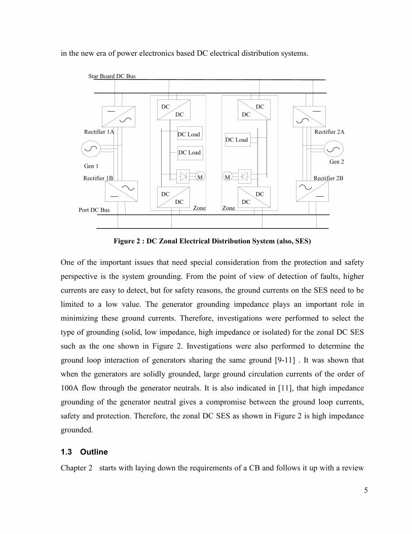
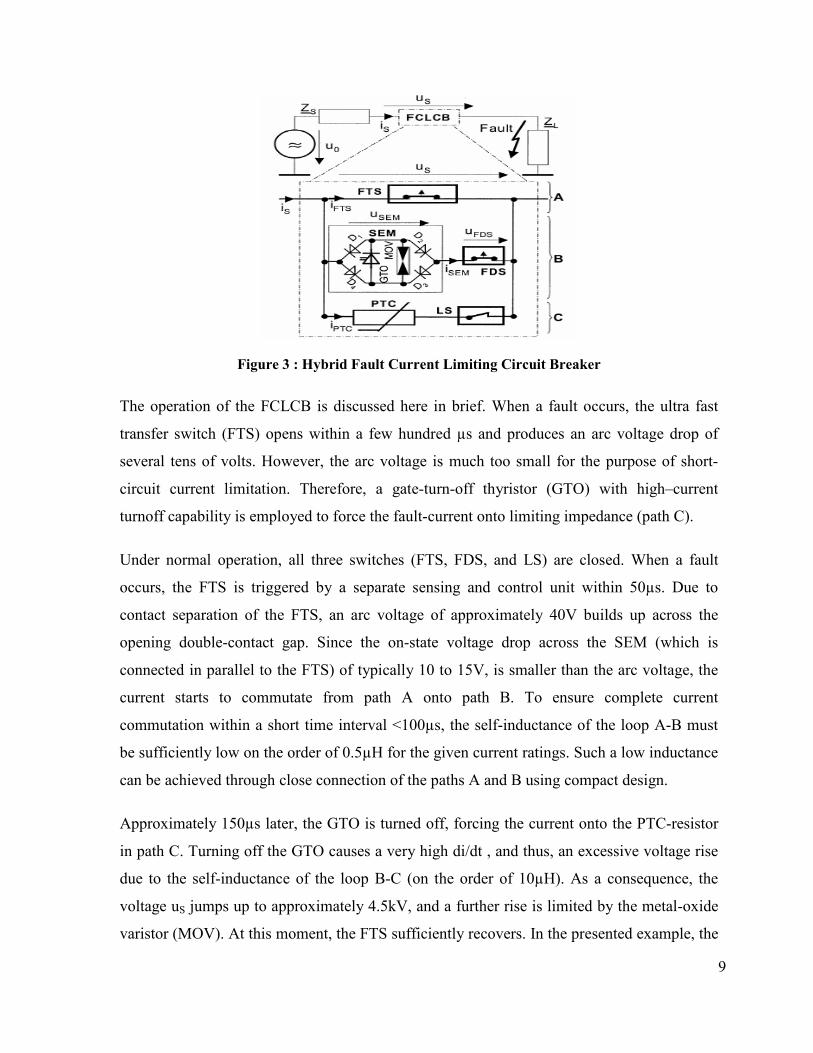
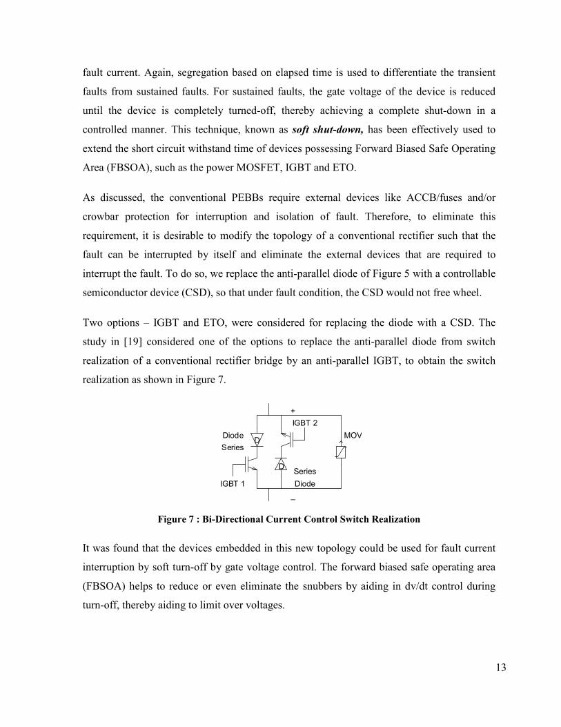
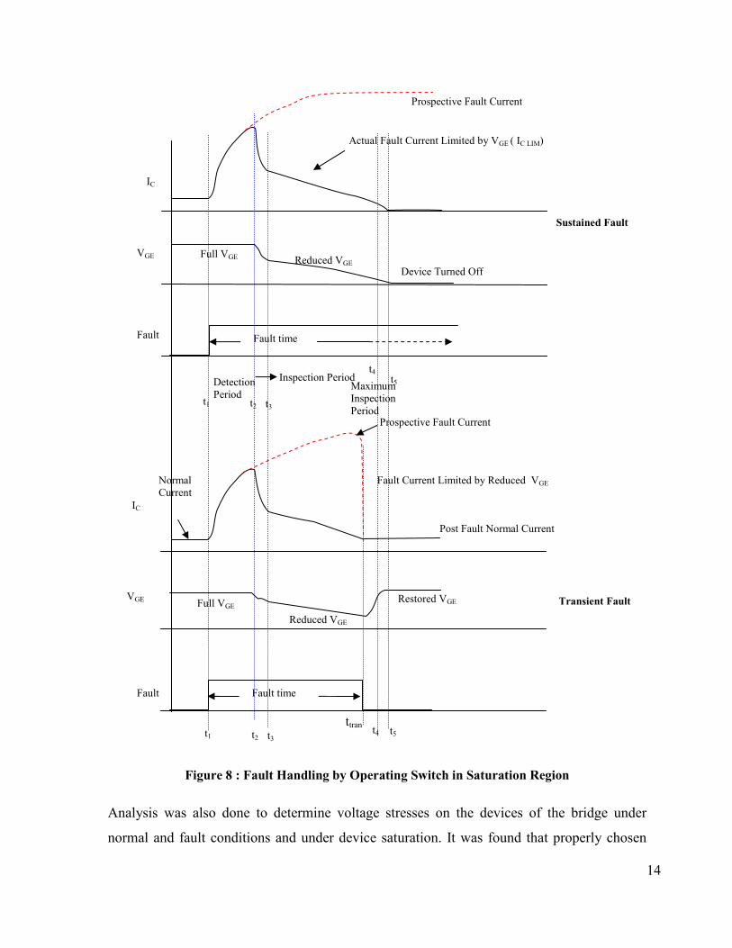
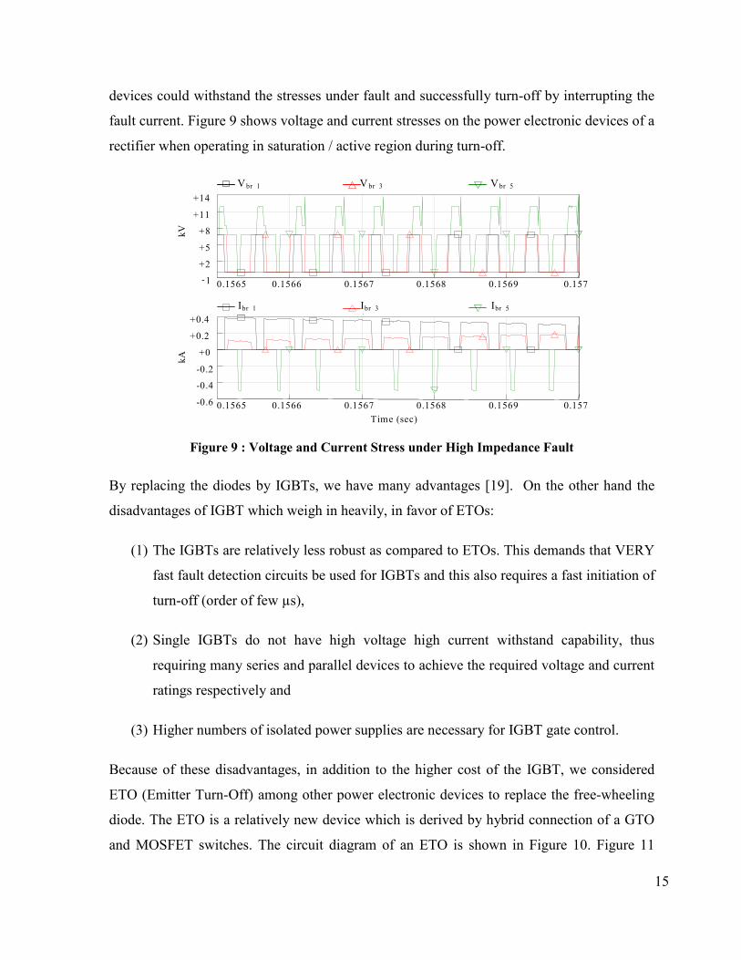
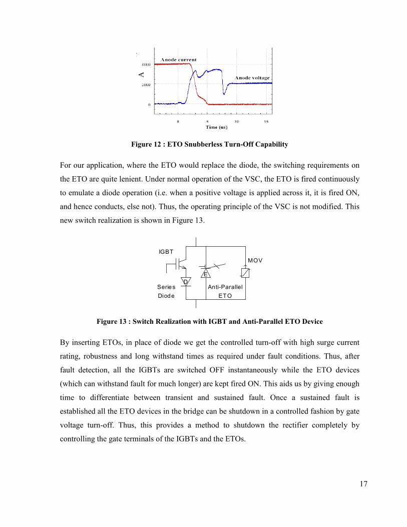
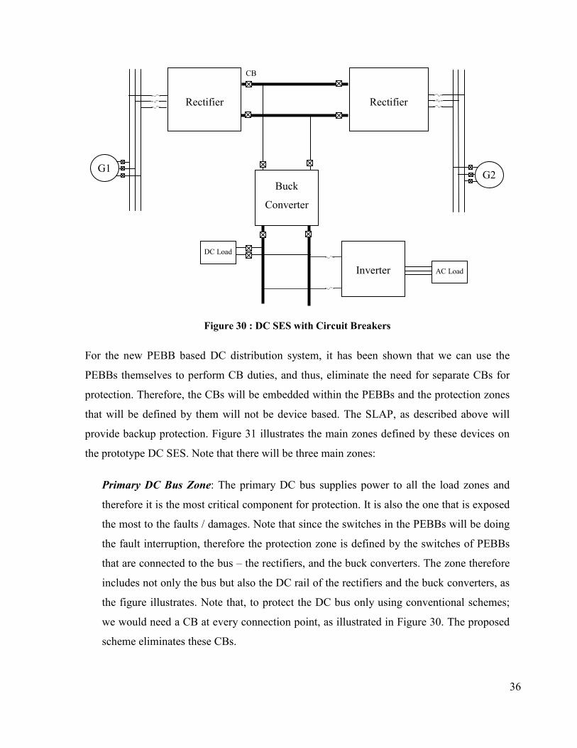
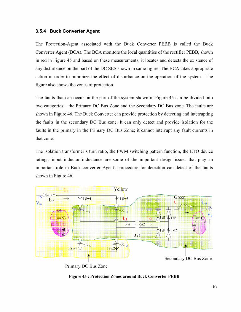
ABSTRACT
MAHAJAN, NIKHIL RAVINDRA. System Protection for Power Electronic Building Block
Based DC Distribution Systems. (Under the direction of Mesut E Baran)
The purpose of this research has been to develop an agent based protection and
reconfiguration scheme for power electronic building block based (PEBB) DC distribution
systems. One of the foremost applications would be in the new zonal DC distribution on
naval ships. The research involves the design of an agent based protection scheme which
uses the PEBBs for current limiting and circuit breaking purposes. Considerations are given
to reduce the system downtime under fault conditions, allow proper coordination and provide
backup protection. The research also involves the design of a reconfiguration management
scheme based on collaborative agents. The collaboration ensures that the reconfiguration is
achieved at a global level, enhancing the system survivability under the conditions of
multiple faults and damages. The coordination ensures that only the faulted part of the
system is isolated and the reconfiguration makes sure that the power to the healthy part of
the system is supplied continuously. The reconfiguration management also performs load
shedding if the generation does not meet the load demand of the reconfigured system due to a
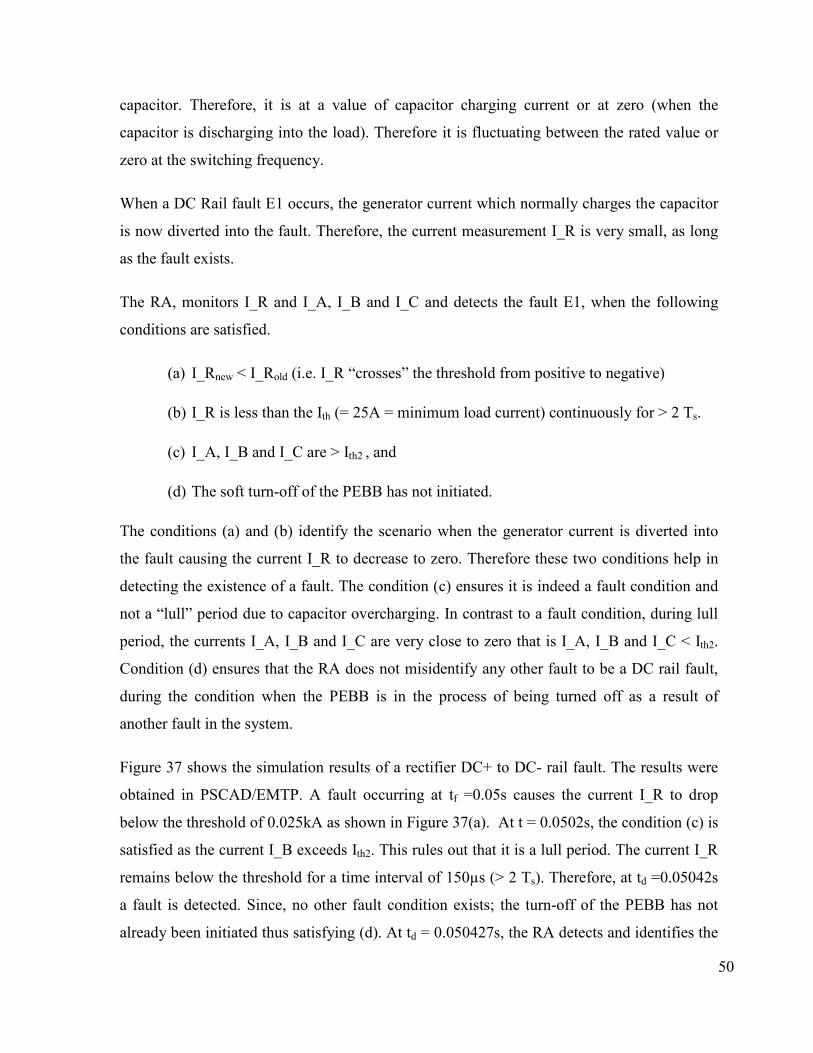
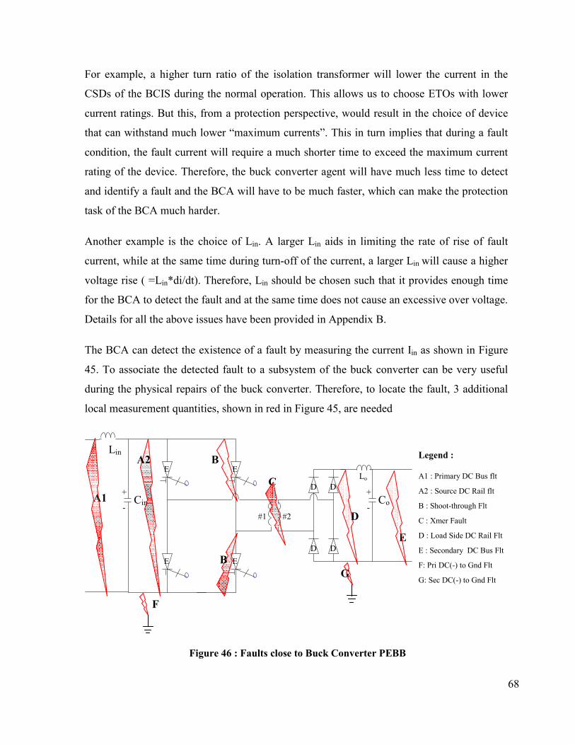
Figure 61 : Remote Backup by RAs for a Transformer Primary Fault
87
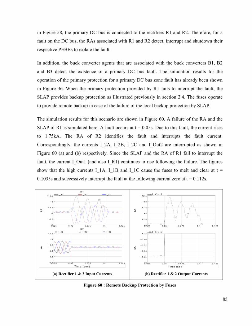
Directly following the fault, the output capacitors of the rectifiers discharge into the fault as
seen by currents I_Out1 and I_Out2 in Figure 61(b) and successively turn off. The fault is
now fed by the generators via the rectifiers. The increasing generators are shown in Figure
61(c). At t=0.0504s when the current I_Out1 and I_Out2 exceeds the RAs threshold, it
detects the fault and turns off to interrupt the fault current.
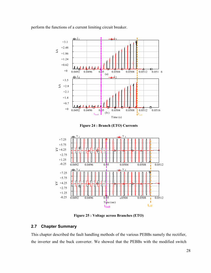
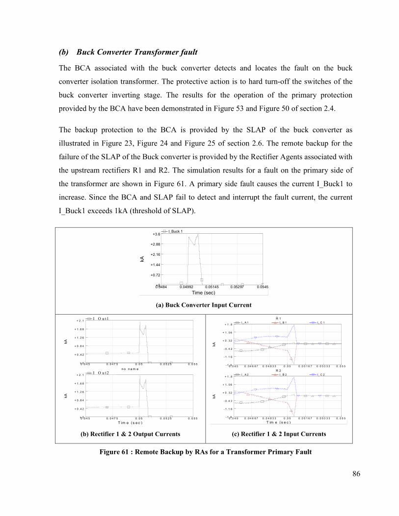
(c) Fault in the Secondary DC Bus Zone
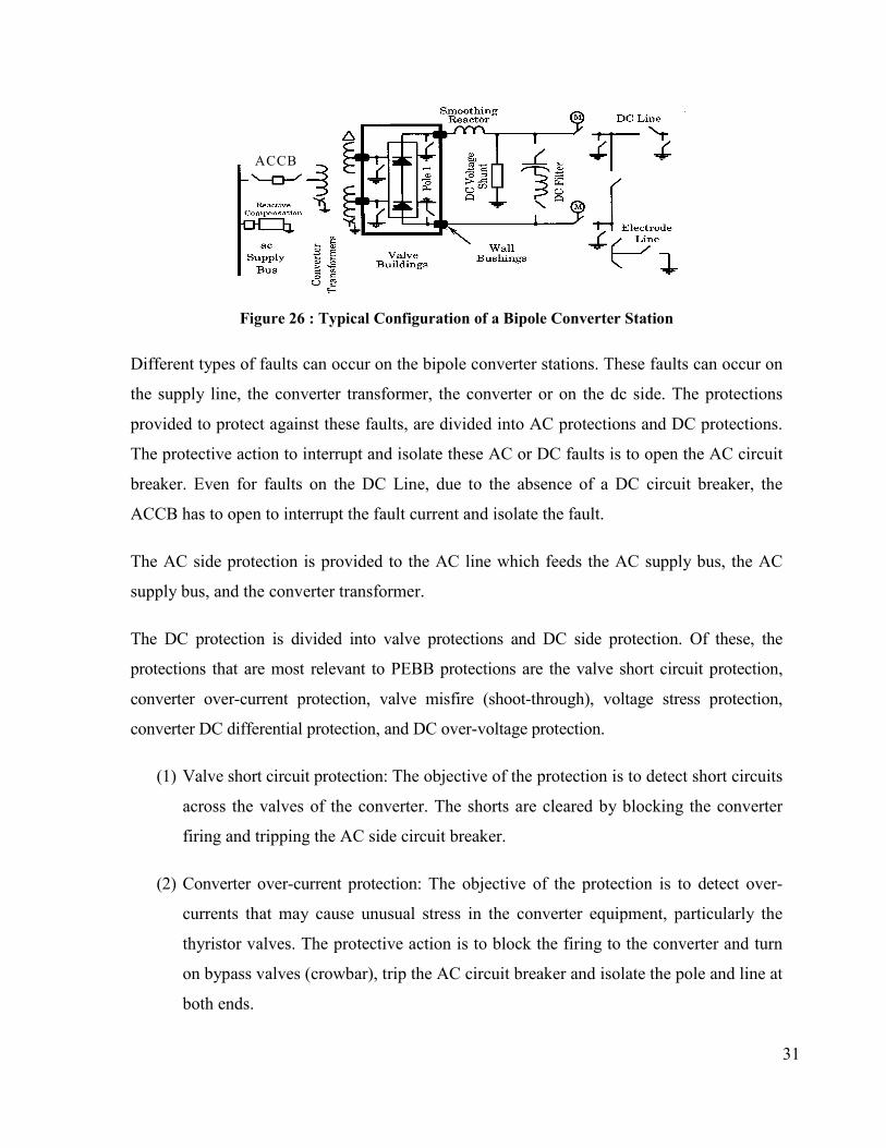
The primary protection for a fault in the secondary DC bus zone is provided by the BCA and
the local backup is provided by the SLAP. A Remote backup is provided by the upstream
rectifiers R1 and R2.
The simulation results are shown in Figure 62. As shown in Figure 62(a), the Buck converter
output (fault) current, I_DC_Sec1 is about 12.5kA and the input side is about 2.5kA, as
shown in Figure 62(b) (with a transformer ratio 5:1). Further, this current is divided equally
among the two supplying rectifiers. Therefore, the current sensed by the RAs is below their
threshold of 1.75kA, shown in Figure 62(c) and (d) and hence the RAs do not detect a fault
condition and do not provide backup protection for SLAP failure of buck converter.
Time (sec)0.049 0.05 0.051 0.052 0.053 0.054 0.055
kA
+0
+2.6
+5.2
+7.8
+10.4
+13I_DC_Sec1
(a) Buck Converter 1 Output Current
Time (sec)0.049 0.05 0.051 0.052 0.053 0.054 0.055
kA
+0
+0.5
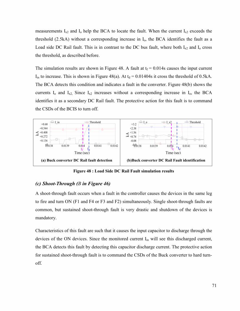
+1
+1.5
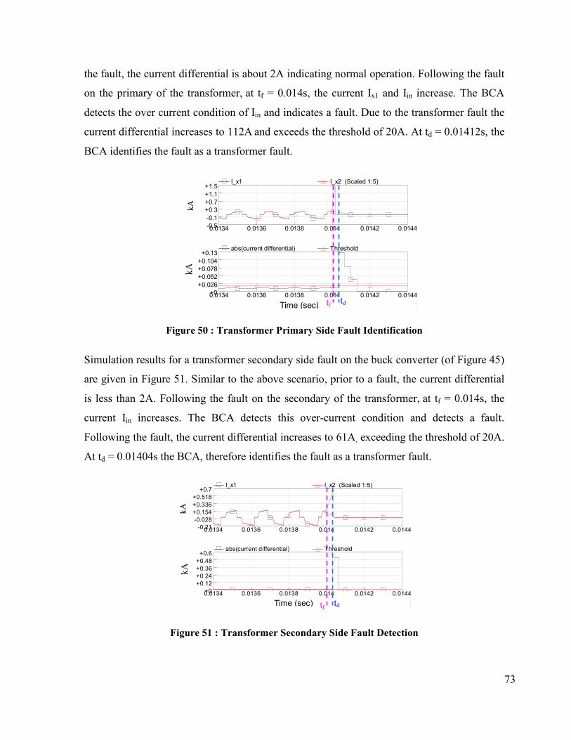
+2
+2.5I_Buck 1
(b) Buck Converter 1 Input Current
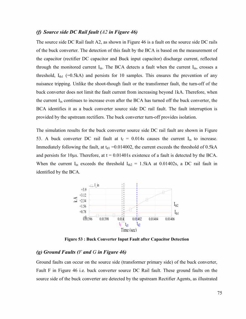
Time (sec)0.049 0.05 0.051 0.052 0.053 0.054 0.055
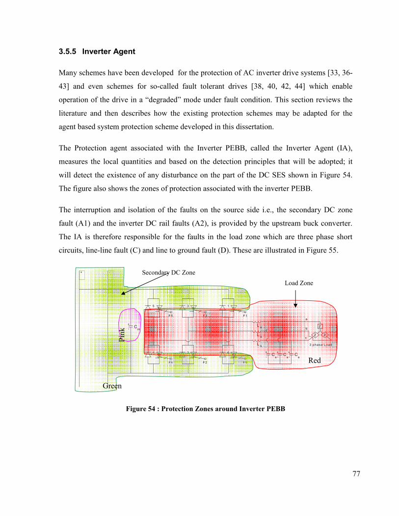
kA
+0.4
+0.64
+0.88
+1.12
+1.36
+1.6I_R1I_Out1
(c) Rectifier 1 Output Current
Time (sec)0.049 0.05 0.051 0.052 0.053 0.054 0.055
kA
+0.4
+0.64
+0.88
+1.12
+1.36
+1.6I_R2I_Out2
(d) Rectifier 2 Output Current
Figure 62 : Buck converter SLAP Failure during a Secondary DC bus zone fault
88
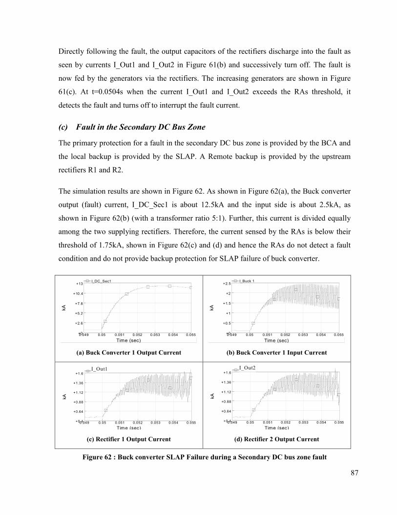
A remedy for this problem is to provide a crowbar device at the input of the buck converter
ensures this. The crowbar however should be turned on only when the SLAP failure occurs.
This is done by noting that the threshold of the SLAP is 1kA, therefore, when the input
current, Iin (Figure 45) of the buck converter exceeds a threshold of 1.25kA, it implies that
the SLAP and the devices have failed to interrupt the fault. Therefore, the crowbar device is
turned on when the current Iin, exceeds the threshold of 1.25kA. This creates a low
impedance path and causes the causes the current I_Out1 and I_Out2 to increase rapidly.
This increased current is then sensed by the RAs and they detect a fault and turn-off the
Rectifiers, thereby providing backup protection.
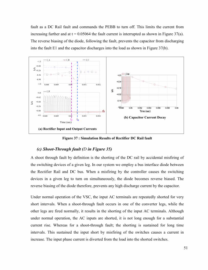
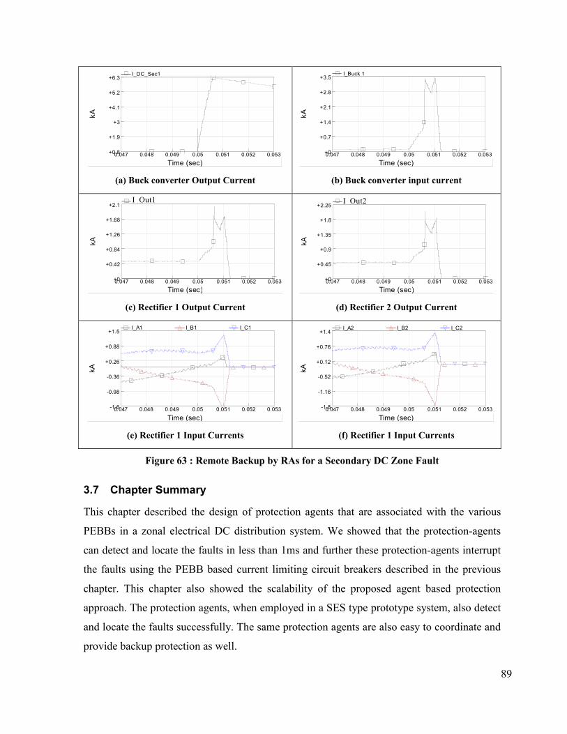
The simulation results are shown in Figure 63. A fault occurring at t = 0.05s causes the buck
converter output current, I_DC_Sec1 and the buck converter input current, I_Buck1 to
increase as seen in Figure 63(a) and (b) respectively. This causes only a marginal increase in
the rectifier output currents, I_R1, I_R2. At t = 0.0505s, the buck converter input current,
I_Buck1 crosses the threshold of 1.25kA. This indicates that the SLAP has failed to interrupt
the fault and therefore the crowbar device is turned on. This causes the buck converter
current I_Buck1, and the rectifier currents, I_R1 and I_R2 to increase sharply. At t = 0.0513s,
I_R1 and I_R2 exceed 1.75kA. The RA detects this and turns the PEBB off, thus providing
backup protection for SLAP failure.
89
Time (sec)0.047 0.048 0.049 0.05 0.051 0.052 0.053
kA
+0.8
+1.9
+3
+4.1
+5.2
+6.3I_DC_Sec1
(a) Buck converter Output Current
Time (sec)0.047 0.048 0.049 0.05 0.051 0.052 0.053
kA
+0
+0.7
+1.4
+2.1
+2.8
+3.5I_Buck 1
(b) Buck converter input current
Time (sec)0.047 0.048 0.049 0.05 0.051 0.052 0.053
kA
+0
+0.42
+0.84
+1.26
+1.68
+2.1I_R1I Out1
(c) Rectifier 1 Output Current
Time (sec)0.047 0.048 0.049 0.05 0.051 0.052 0.053
kA
+0
+0.45
+0.9
+1.35
+1.8
+2.25I_R2I Out2
(d) Rectifier 2 Output Current
Time (sec)0.047 0.048 0.049 0.05 0.051 0.052 0.053
kA
-1.6
-0.98
-0.36
+0.26
+0.88
+1.5I_A1 I_B1 I_C1
(e) Rectifier 1 Input Currents
Time (sec)0.047 0.048 0.049 0.05 0.051 0.052 0.053
kA
-1.8
-1.16
-0.52
+0.12
+0.76
+1.4I_A2 I_B2 I_C2
(f) Rectifier 1 Input Currents
Figure 63 : Remote Backup by RAs for a Secondary DC Zone Fault
3.7 Chapter Summary
This chapter described the design of protection agents that are associated with the various
PEBBs in a zonal electrical DC distribution system. We showed that the protection-agents
can detect and locate the faults in less than 1ms and further these protection-agents interrupt
the faults using the PEBB based current limiting circuit breakers described in the previous
chapter. This chapter also showed the scalability of the proposed agent based protection
approach. The protection agents, when employed in a SES type prototype system, also detect
and locate the faults successfully. The same protection agents are also easy to coordinate and
provide backup protection as well.
90
4 RECONFIGURATION MANAGEMENT
4.1 Introduction and Overview
The Protection-Agents of the new Agent based System Protection scheme monitor the local
quantities to detect and isolate the disturbances. In response to the disturbances, the same
agents then collaborate with each other to reconfigure the system. The protective action
(based solely on the local variables) ensures that the protection is very fast, whereas the
reconfiguration, which is a collaborative action, ensures that the re-configuration is achieved
globally at a system level. Thus, it provides shorter system downtime and minimum number
of components outage.
The first primary task of system protection was detailed in the previous chapter. This chapter
deals with the second task of reconfiguration management which ensures service continuity
to the unfaulted part of the system.
Reconfiguration is the action performed, typically the opening or closing of switches,
sectionalizers and/or CBs, subsequent to the isolation of faults, to maximize power delivery
to the unfaulted sections of the system, without exceeding the rated limits [45] of the system
components (generators, lines etc).
4.2 Agent Based Collaborative Reconfiguration
4.2.1 Objectives and Requirements
The main objective of performing reconfiguration on a system is to maintain the availability
of power to all connected loads in order to keep all the system and equipment operational.
Under abnormal conditions, the power to only the smallest affected /faulted portion of the
system should be interrupted [46]. The main goal, therefore, of an automated
reconfiguration such as the one designed here for the SES, is to increase the survivability of
the SES under faults and battle conditions, eliminate human errors, make reconfiguration
decisions more quickly and provide optimal electric power service through the surviving
electrical system [46].
91
For a SES like zonal electrical distribution system, it is further desired that the
reconfiguration system can seamlessly transfer power to an alternate source since a small
interruption in power to equipment like weapons system may have catastrophic results [6].
The zonal architecture of the SES further aids in achieving this.
4.2.2 Contingencies
The faults on the SES could be due to material casualty of individual loads or widespread
damage due to battle damage. In addition to load faults, casualty can occur to cables, power
generating equipment or power distribution buses. Some equipment failures and battle
damages may lead to large over-current conditions. Battle damage may also generate
multiple faults in contiguous areas.
For the prototype system shown in Figure 58, the contingencies for which the agent based
protection scheme has detected and isolated the fault and the for which reconfiguration is
desired are : generator fault /damage, Primary DC Bus damage, Rectifier fault / damage,
Zone flooding, Secondary DC bus fault / damage, Buck Converter fault / damage and load
damage.
These contingencies can lead to conditions of having inadequate power generation capacity
to all attached loads. Therefore, connecting additional backup generators may be necessary.
Load shedding is another option when backup generation is not available. A load priority list,
with the critical loads having high priority and the non-critical loads with low priority is
available for a SES. Load shedding is performed by disconnecting the low-priority loads
followed by disconnecting the medium priority and then the high priority loads, in that order.
This is done until the generation matches or exceeds the connected loads.
4.2.3 Agent Based Reconfiguration
As discussed earlier, the zonal architecture of the SES is unique and a proper design and
choice of some of the design issues can considerably enhance the reconfigurability of the
SES under faults and battle damages. These design consideration include the choice of
number of the sectionalizers, the location of the sectionalizers, the normal state of the
92
sectionalizers, choice of number of generators, and the secondary DC bus configuration.
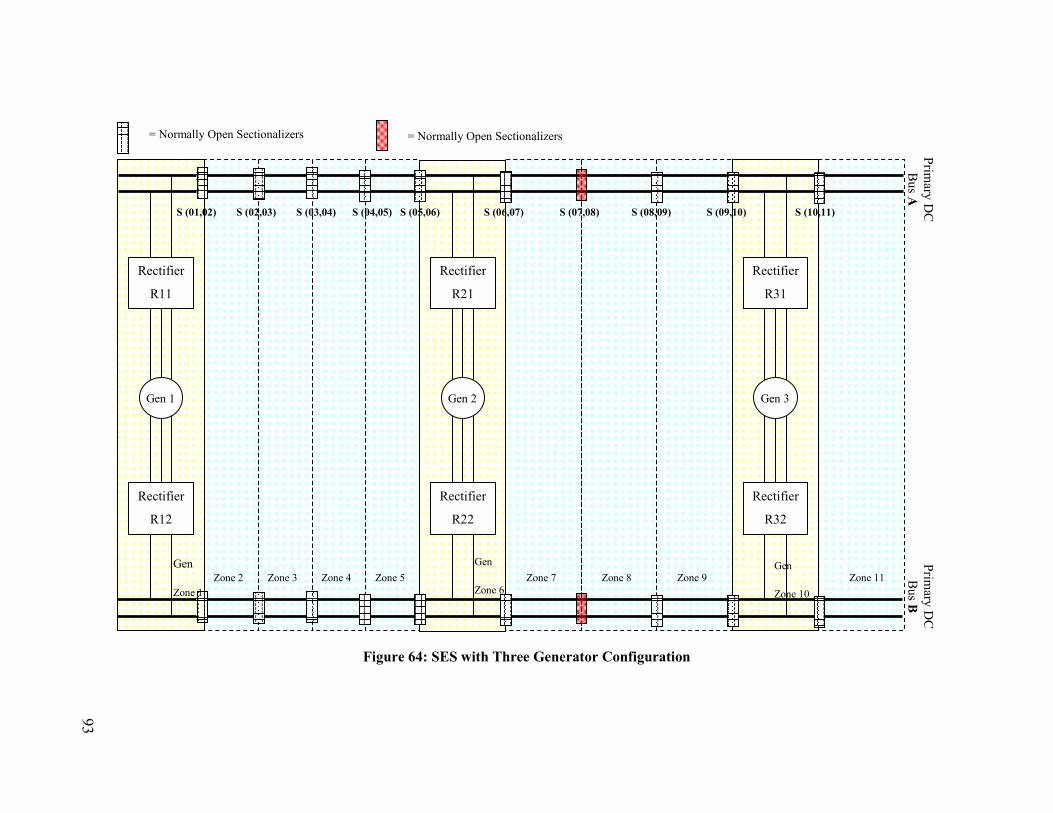
Normally closed and normally open sectionalizers are provided selectively in the designed
prototype SES as shown in Figure 64. Normally closed sectionalizers are provided for each
zone. They can be opened during reconfiguration when a DC bus zone fault or zone flooding
is detected. This would help to isolate a given zone (after the protection agents have detected
and interrupted the fault, and de-energized the bus) so that the adjacent zones are not
affected. Providing sectionalizers will ensure that only the zone affected by battle damage or
zone flooding can be isolated individually. This minimizes the number of system components
without power. The normally open sectionalizers are provided to improve system
survivability under the condition of multiple DC bus fault due to war damage like conditions.
The intra zonal configuration of the secondary DC buses is shown in Figure 65. The Buck
converters interface the primary DC bus to the secondary DC bus. The vital or the critical
loads are fed by auctioneering diodes as illustrated in Figure 65. The auctioneering diodes
ensure that the transfer of power from main bus to alternate bus is seamless and without
interruption. To allow the proper operation of the auctioneering scheme, the output of the
buck converters fed from the alternate bus is kept just below (at 750V) the output of the buck
converter from the main bus (800V). The converter module or the inverter module which
interfaces the load to the secondary bus absorbs the glitch when the power is transferred from
one bus to the other, therefore making the transfer appear seamless to the load. In addition,
the two buck converter agents of the given zone collaborate with each other, so that when the
power is transferred from the main bus to the alternate bus, the output of the alternate buck
converter is raised to 800V.
Different scenarios of faults and battle damage are considered in this section. It is shown that
the power is transferred seamlessly from the main DC bus to the alternate DC bus following
a fault and that the agents reconfigure the system to improve the survivability of the SES.
The steps/procedures involved in reconfiguration for the main faults are described below.
93
Figure 64: SES with Three Generator Configuration
Rectifier
R11
Rectifier
R12
Rectifier
R21
Rectifier
R22
Rectifier
R31
Rectifier
R32
Gen 1 Gen 2 Gen 3
= Normally Open Sectionalizers= Normally Open SectionalizersPrim
ary DC
B
us APrim
ary DC
B
us B
Zone 2 Zone 3 Zone 4 Zone 5 Zone 7 Zone 8 Zone 9 Zone 11Gen
Zone 1
Gen
Zone 10
Gen
Zone 6
S (02,03) S (03,04) S (04,05) S (05,06) S (07,08) S (08,09) S (09,10)S (01,02) S (10,11)S (06,07)
94
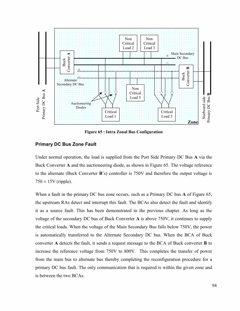
Figure 65 : Intra Zonal Bus Configuration
Primary DC Bus Zone Fault
Under normal operation, the load is supplied from the Port Side Primary DC Bus A via the
Buck Converter A and the auctioneering diode, as shown in Figure 65. The voltage reference
to the alternate (Buck Converter B’s) controller is 750V and therefore the output voltage is
750 ± 15V (ripple).
When a fault in the primary DC bus zone occurs, such as a Primary DC bus A of Figure 65,
the upstream RAs detect and interrupt this fault. The BCAs also detect the fault and identify
it as a source fault. This has been demonstrated in the previous chapter. As long as the
voltage of the secondary DC bus of Buck Converter A is above 750V, it continues to supply
the critical loads. When the voltage of the Main Secondary Bus falls below 750V, the power
is automatically transferred to the Alternate Secondary DC bus. When the BCA of Buck
converter A detects the fault, it sends a request message to the BCA of Buck converter B to
increase the reference voltage from 750V to 800V. This completes the transfer of power
from the main bus to alternate bus thereby completing the reconfiguration procedure for a
primary DC bus fault. The only communication that is required is within the given zone and
is between the two BCAs.
Buc
kC
onve
rterA
Critical Load 1
Critical Load 3
Non Critical Load 5
Buc
kC
onve
rterB
Non Critical Load 2
Non Critical Load 3
Port
Side
Prim
ary
DC
Bus
A
Star
boar
dsi
dePr
imar
yD
CB
usB
Zone
Main Secondary DC Bus
Alternate Secondary DC Bus
Auctioneering Diodes
+−
+−
95
Secondary DC Bus Zone Fault
A fault on the main secondary DC bus will cause its voltage to collapse. This fault is detected
by the BCA Buck converter A and similar to the previous scenario, the BCA A sends a
request message to the BCA B to increase the reference voltage from 750 to 800V. Similar to
the previous scenario, the supply of power is transferred from the main bus to the alternate
bus automatically and seamlessly, when the voltage of the main secondary DC Bus A falls
below 750V. The secondary DC bus zone fault in one zone does not affect the loads in the
other zone at all.
Buck Converter Source Side DC Rail Fault
A Buck Converter source side DC Rail fault is a fault in the Primary DC Bus zone and the
normally closed (NC) sectionalizers employed on the primary DC Bus can be effectively
used to isolate the only affected zone. The reconfiguration for this fault in the primary DC
bus zone is, therefore, different from the configuration performed for a fault on the Primary
DC bus.
The Buck Converter source side DC rail fault is detected and interrupted by the RAs of the
upstream Rectifiers. The BCA of the buck converter locates this fault to its input DC rails.
This additional information is used advantageously for reconfiguration of the system under
multiple fault condition.
The reconfiguration action performed for a single fault -a Buck converter source side DC
Rail fault, is similar to the DC bus fault described above. The interruption of the fault by the
RAs and the shutdown of the Buck converter cause the output voltage of the Buck converter
to decay. Therefore the voltage of Buck converter A falls below 750V and the supply of
power is transferred from the port side primary DC Bus A to the starboard primary DC bus
B, thereby completing the reconfiguration for the single fault.
Another important scenario which adds challenge to the Buck converter source side DC rail
fault is the occurrence of a second successive fault on the alternate primary DC bus B. Under
such a scenario of two successive faults, one fault on the buck converter source side DC rail
96
fault of the port side primary DC bus A and another bus fault on the starboard primary DC
bus B, the whole system would need to be shutdown. The additional information gathered
previously is used to avoid such a catastrophic failure. For this scenario of multiple fault
condition, a solution is proposed so that the selective NO sectionalizers are opened to
sectionalize the first fault (buck converter source side DC rail fault). Therefore for a
successive second fault on the primary DC bus B, the power can be re-transferred back to the
primary DC bus A, avoiding a total shut-down or collapse of the system. This considerably
improves the system survivability under multiple fault conditions.
This is explained by an illustration. Let us consider that a Buck input DC rail fault in zone 5
occurs for the system shown in Figure 64. The RAs of Rectifier R11 and R21 detect and
interrupt this fault. The BCA A of zone 5 also detects this fault and identifies it as a buck
converter source side DC rail fault. The BCA A then sends a request message for to the BCA
B to increase the reference voltage to 800V. The power is thus transferred to the alternate bus
B and the primary DC bus A is de-energized. Now, for a subsequent fault on the DC bus B of
Figure 64, the complete system will be shutdown by the Rectifiers R11, R12, R21 and R22.
To avoid such a system shutdown, following the detection and location of the buck converter
source side DC rail fault (of the primary DC bus A), the BCA A, sends a request to open the
sectionalizers S(04,05) and S(05,06), as soon as the R11 and R21 have interrupted the fault
and de-energized the bus A. The opening of the sectionalizers isolates the faulted zone.
For a subsequent fault on the primary DC bus B, power can be re-transferred back to the
healthy part of the primary DC bus A, since the opening the sectionalizers has isolated the
faulted part of the system. Hence, the agent based reconfiguration scheme prevents a total
system collapse and improves the system survivability under war damage conditions such as
multiple faults.
The opening of the above mentioned sectionalizers may also create another challenge of
generation-load mismatch. In the reconfigured system, the Gen1 supplies power to the zones
1 through 4 while the Gen2 supplies power to zones 6 and 7. It may be possible that the
generation of Gen1 or Gen2 is not sufficient to meet all the loads of zones 1-4 or 6-7
respectively. Therefore, when a BCA requests the opening of sectionalizers, it also initiates a
97
load flow to match the load with the generation and if necessary a load shedding algorithm is
initiated, as explained previously. This ensures that the generators of the reconfigured system
are not overloaded.
Fault in Zone 9
Similar to the scenario of successive faults discussed above, another challenging fault is a
fault in the Zone 9 of Figure 64. Under the normal operation of the system, Gen3 supplies
power to zones 8-11 as S(07,08) is normally open, while, Gen1 and Gen2 supply power to
Zones 1-7.
Let us assume that primary DC Bus B has been de-energized due to a pre-existing fault.
When a successive Buck converter source side DC rail fault occurs in Zone 9, the upstream
rectifiers detect and interrupt the fault current and the BCA of Zone 9 identifies this fault as a
source fault. The BCA also sends a request to open the sectionalizers S(08,09) and S(09,10).
The opening of these sectionalizers isolates the faulted zone. But, in addition, opening of
these 2 sectionalizers also unnecessarily interrupts power to zone 8. Therefore additional
actions are needed to avoid the unnecessary interruption of power to Zone 8.
The sequence of actions that the BCA should take when a buck converter source side DC rail
fault occurs in Zone 9, in order to avoid interruption of power to the zone 8 are:
(1) Send a request message to the alternate BCA of the same zone to increase the
reference voltage from 750 to 800V,
(2) Send a request message to open the NC sectionalizers S(08,09) and
(3) Send a message to the BCA of the adjacent zones (zone 9 and zone 10) to ensure that
at least one of the sectionalizers connected to those zones are closed. For this
particular example, both the sectionalizers of Zone 8 are open. Therefore, in addition
to these actions taken by the BCA of Zone 9, the BCA of zone 8 requests the NO
sectionalizer S(07,08) to be closed. This ensures that power is supplied to Zone 8 via
Gen1 and Gen2, thus maintaining the continuity of supply to all but the faulted zone.
98
(4) Lastly, due to the closing of the NO sectionalizer S(07,08) it may be possible that the
generation capacity of Gen1 and Gen2 is insufficient to meet all the loads of Zone 1
through Zone 8. Therefore, load shedding may be required.
Generation Failure
The last fault condition that is addressed here is a fault or damage in one of the generators.
The RAs of the rectifiers detect a zero input current condition and identify it as a generator
fault. When such a generator fault is detected, the RAs request the closing of the NO
sectionalizer S(07,08), and initiate load shedding to match the load demand with the
generation (Gen2 and Gen3). This completes the reconfiguration for a generation failure.
The following part of this section illustrates the system reconfiguration procedures described
above. Simulation results are shown for two of the most common faults – Primary DC Bus
fault and Secondary DC Bus fault. The prototype system for reconfiguration is shown in
Figure 66. It has a main primary DC bus A and alternate primary DC Bus B. Every critical
load within a zone is fed by both the intra-zonal secondary DC Buses A and B, while the
non-critical loads are supplied power by only either of the secondary DC buses.
Figure 66 : Prototype System for Reconfiguration
Primary DC Bus A
R1A
G1
B1A
Critical Load 1
Zone 1
7kV DC Load
B1B
Non-Critical Load
Non-Critical Load
B2A
Critical Load 2
Zone 2
B2B
Non-Critical Load
Non-Critical Load
R1B
Seco
ndar
yD
CB
usA
Seco
ndar
yD
CB
usB
DCDC
DCDC
DCDC
DCDC
99
Scenario 1: Primary DC Bus Fault
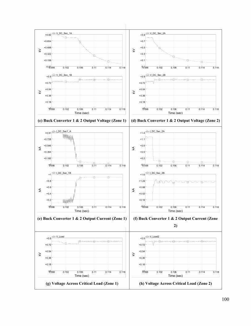
Simulation results for a fault on the primary DC bus A at t = 0.1s are shown in Figure 67.
Following the fault, the output voltage of R1A, V_R1 (Figure 59) collapses, as shown in
Figure 67(a). Correspondingly, the current, I_R1 (Figure 59) rises as shown in Figure 67(b).
The fault is detected by the RA of R1A and it shuts down the Rectifier R1A of Figure 66.
Following the shutdown, the voltages of the secondary DC Bus A of both zones 1 and 2
(V_DC_Sec_1A and V_DC_Sec_2A) start decaying. This is seen in Figure 67(c) and (d).
When the BCA of B1A and B2A detect the source fault, they send a message to B1B and
B2B respectively to increase the reference voltage from 750V to 800V. Therefore, the
voltages V_DC_Sec_1B and V_DC_Sec_2B increase from 750 to 800V as seen in Figure
67(c) and (d). The BCA of B1A detects the fault at t = 0.01055s, therefore, it is seen that the
loads of zone 1 see the voltage dip for a transient time interval of 0.0056s. The voltage dip is
less than 8%. The BCA of B2A detects the source fault much earlier at t = 0.101s, and
therefore sends the message to the BCA of B2B to increase the voltage within 0.001s,
therefore the loads of zone 2 see the voltage dip for about 0.001s. The rise in the voltage
V_DC_Sec_2B causes the load current to be commutated from the secondary DC bus A to
the secondary DC bus B as seen in Figure 67(e) and (f). The voltage across the loads of the
zone 1 and zone 2 are shown in Figure 67(g) and (h) and the load currents of zone 1 and 2 are
shown in Figure 67(i) and (j) respectively.
Time (sec)
0.098 0.102 0.106 0.11 0.114 0.118
kV
+0
+1.45
+2.9
+4.35
+5.8
+7.25V_R1
0.098 0.102 0.106 0.11 0.114 0.118
kV
+0
+1.45
+2.9
+4.35
+5.8
+7.25V_R2
(a) Rectifier 1 & 2 Output DC Voltages
Time (sec)
0.098 0.102 0.106 0.11 0.114 0.118
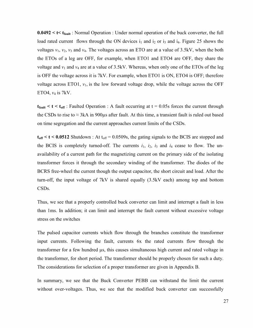
kA
+0
+0.42
+0.84
+1.26
+1.68
+2.1I_Out1
0.098 0.102 0.106 0.11 0.114 0.118
kA
+0
+0.162
+0.324
+0.486
+0.648
+0.81I_Out2
(b) Rectifier 1 &2 Output Currents
100
Time (sec)
0.098 0.102 0.106 0.11 0.114 0.118
kV
-0.01
+0.156
+0.322
+0.488
+0.654
+0.82V_DC_Sec_1A
0.098 0.102 0.106 0.11 0.114 0.118
kV
+0
+0.18
+0.36
+0.54
+0.72
+0.9V_DC_Sec_1B
(c) Buck Converter 1 & 2 Output Voltage (Zone 1)
Time (sec)
0.098 0.102 0.106 0.11 0.114 0.118
kV
-0.1
+0.1
+0.3
+0.5
+0.7
+0.9V_DC_Sec_2A
0.098 0.102 0.106 0.11 0.114 0.118
kV
+0
+0.18
+0.36
+0.54
+0.72
+0.9V_DC_Sec_2B
(d) Buck Converter 1 & 2 Output Voltage (Zone 2)
Time (sec)
0.098 0.102 0.106 0.11 0.114 0.118
kA
+0
+0.182
+0.364
+0.546
+0.728
+0.91I_DC_Sec1_A
0.098 0.102 0.106 0.11 0.114 0.118
kA
+0
+0.2
+0.4
+0.6
+0.8
+1I_DC_Sec_1B
(e) Buck Converter 1 & 2 Output Current (Zone 1)
Time (sec)
0.098 0.102 0.106 0.11 0.114 0.118
kA
-0.1
+0.2
+0.5
+0.8
+1.1
+1.4I_DC_Sec_2A
0.098 0.102 0.106 0.11 0.114 0.118
kA
-0.2
+0.16
+0.52
+0.88
+1.24
+1.6I_DC_Sec_2B
(f) Buck Converter 1 & 2 Output Current (Zone
2)
Time (sec)0.098 0.102 0.106 0.11 0.114 0.118
kV
+0
+0.18
+0.36
+0.54
+0.72
+0.9V_Load
(g) Voltage Across Critical Load (Zone 1)
Time (sec)0.098 0.102 0.106 0.11 0.114 0.118
kV
+0
+0.18
+0.36
+0.54
+0.72
+0.9V_Load2
(h) Voltage Across Critical Load (Zone 2)
101
Time (sec)0.098 0.102 0.106 0.11 0.114 0.118
kA
+0
+0.17
+0.34
+0.51
+0.68
+0.85I_Load
(i) Critical Load Current (Zone 1)
Time (sec)0.098 0.102 0.106 0.11 0.114 0.118
kA
+0
+0.32
+0.64
+0.96
+1.28
+1.6I_Load2
(j) Critical Load Current (Zone 2)
Figure 67 : Reconfiguration Results for Primary DC Bus Fault
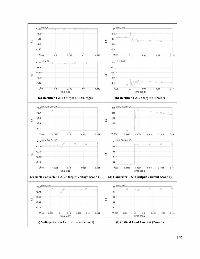
Scenario 2: Secondary DC Bus Fault
A fault on the secondary DC bus A of zone 1 has been simulated here. The results are shown
in Figure 68. The voltages of the primary DC bus A and bus B are shown in Figure 68(a).
Prior to the fault at t = 0.01s, the loads of Zone 1 are fed via G1->R1A->B1A-> Critical
Load1 (Figure 65). Following the fault, the loads of zone 1 are transferred from primary DC
Bus A to primary DC Bus B. Therefore the loads are now supplied via G1->R1B-> B1B->
Critical Load1. The loads of zone 2 are continuously supplied from primary DC bus A, via
R2A-> B2A -> Critical Load2. This causes a decrease in current supplied by R1A (I_Out1,
Figure 34) and the corresponding increase in current (I_Out2, Figure 34) supplied by R1B. It
is seen in Figure 68(b). Subsequent to the fault on the secondary DC bus A of Zone 1; the
voltage V_DC_Sec_1A collapses and the current I_DC_Sec_1A increases. This is shown in
Figure 68(c) and (d) respectively. The BCA of B1A detects the DC bus fault and sends a
message to the BCA of B1B in about 0.0004s to increase the voltage V_DC_Sec_1B, from
750V to 800V. Therefore, load experiences a voltage and current dip as seen in Figure 68(e)
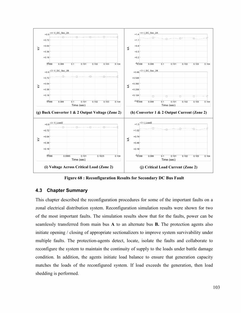
and (f) respectively for 0.0004s. Figure 68(g), (h), (i) and (j) show the voltages and currents
profiles for zone 2. These figures indicate that the state of the second zone is not affected in
any way, due to the fault in the Zone 1, and therefore does not require any reconfiguration.
These simulation results demonstrate the effectiveness of a reconfiguration scheme under 2
of the most commons faults –the primary and the secondary DC bus fault. The
reconfiguration scheme is able to seamlessly transfer power from the main bus to an alternate
bus.
102
Time (sec)
0.095 0.1 0.105 0.11 0.115
kV
+0
+1.45
+2.9
+4.35
+5.8
+7.25V_R1
0.095 0.1 0.105 0.11 0.115
kV
+0
+1.45
+2.9
+4.35
+5.8
+7.25V_R2
(a) Rectifier 1 & 2 Output DC Voltages
Time (sec)
0.095 0.1 0.105 0.11 0.115
kA
+0
+0.18
+0.36
+0.54
+0.72
+0.9I_Out1
0.095 0.1 0.105 0.11 0.115
kA
+0
+0.18
+0.36
+0.54
+0.72
+0.9I_Out2
(b) Rectifier 1 & 2 Output Currents
Time (sec)
0.098 0.0995 0.101 0.1025 0.104
kV
-0.1
+0.1
+0.3
+0.5
+0.7
+0.9V_DC_Sec_1A
0.098 0.0995 0.101 0.1025 0.104
kV
+0
+0.18
+0.36
+0.54
+0.72
+0.9V_DC_Sec_1B
(c) Buck Converter 1 & 2 Output Voltage (Zone 1)
Time (sec)
0.098 0.0992 0.1004 0.1016 0.1028 0.104
kA
+0.75
+1.15
+1.55
+1.95
+2.35
+2.75I_DC_Sec1_A
0.098 0.0992 0.1004 0.1016 0.1028 0.104
kA
+0
+0.2
+0.4
+0.6
+0.8
+1I_DC_Sec_1B
(d) Converter 1 & 2 Output Current (Zone 1)
Time (sec)0.098 0.099 0.1 0.101 0.102 0.103 0.104
kV
+0
+0.18
+0.36
+0.54
+0.72
+0.9V_Load
(e) Voltage Across Critical Load (Zone 1)
Time (sec)0.098 0.099 0.1 0.101 0.102 0.103 0.104
kA
-0.1
+0.1
+0.3
+0.5
+0.7
+0.9I_Load
(f) Critical Load Current (Zone 1)
103
Time (sec)
0.098 0.099 0.1 0.101 0.102 0.103 0.104
kV
+0
+0.18
+0.36
+0.54
+0.72
+0.9V_DC_Sec_2A
0.098 0.099 0.1 0.101 0.102 0.103 0.104
kV
+0
+0.18
+0.36
+0.54
+0.72
+0.9V_DC_Sec_2B
(g) Buck Converter 1 & 2 Output Voltage (Zone 2)
Time (sec)
0.098 0.099 0.1 0.101 0.102 0.103 0.104
kA
-0.1
+0.2
+0.5
+0.8
+1.1
+1.4I_DC_Sec_2A
0.098 0.099 0.1 0.101 0.102 0.103 0.104
kA
-0.01
+0.124
+0.258
+0.392
+0.526
+0.66I_DC_Sec_2B
(h) Converter 1 & 2 Output Current (Zone 2)
Time (sec)0.098 0.0995 0.101 0.1025 0.104
kV
+0
+0.18
+0.36
+0.54
+0.72
+0.9V_Load2
(i) Voltage Across Critical Load (Zone 2)
Time (sec)0.098 0.099 0.1 0.101 0.102 0.103 0.104
kA
-0.1
+0.18
+0.46
+0.74
+1.02
+1.3I_Load2
(j) Critical Load Current (Zone 2)
Figure 68 : Reconfiguration Results for Secondary DC Bus Fault
4.3 Chapter Summary
This chapter described the reconfiguration procedures for some of the important faults on a
zonal electrical distribution system. Reconfiguration simulation results were shown for two
of the most important faults. The simulation results show that for the faults, power can be
seamlessly transferred from main bus A to an alternate bus B. The protection agents also
initiate opening / closing of appropriate sectionalizers to improve system survivability under
multiple faults. The protection-agents detect, locate, isolate the faults and collaborate to
reconfigure the system to maintain the continuity of supply to the loads under battle damage
condition. In addition, the agents initiate load balance to ensure that generation capacity
matches the loads of the reconfigured system. If load exceeds the generation, then load
shedding is performed.
104
5 CONCLUSIONS
A PEBB based DC distribution system like the SES can be comprehensively protected by the
agent based protection scheme. The time for detection and interruption of faults by the
protection-agents is less than 1ms. The reconfiguration management ensures the continuity of
power supply to the connected loads subsequent to faults and action by the protection-agents.
5.1 Contributions
Previous work [11, 47] by the author showed that it is feasible to develop a distribution
system simulator using a general purpose EMTP program, and the development of such a
simulator was essential in investigation of the issues associated with the new systems that use
power-electronic devices.
Some of the main contributions made in this study involve the following:
1. Investigation of System Design Issues:
Many design issues were investigated. These included the generator grounding, the
modified switch realization for the rectifier and the buck converter, buck converter design
issues for protection, intra-zonal secondary DC bus architecture, and design issues such
as use of auctioneering and bus-rail interface diodes. Other design issues were also
investigated, which allow for proper coordination among various PEBBs such as number
and placement of sectionalizers, number of generators.
For the investigations, the prototype simulator was used. The simulator was enhanced by
adding new models to the PSCAD library. One important model that has been added
during this research is an interpolating model for representing the operation of the ETO
during soft turn-off. The ETO is modeled as a non-linear resistor which is changed piece-
wise linearly (interpolated) based on the current through the device and the voltage across
it. Another model that has been developed is the fuse model. The fuse is modeled as a
resistor and the energy dissipated in the fuse is calculated and compared with the energy
required to melt and clear the fuse to open a CB.
105
2. PEBB based Current limiting CBs:
The work shows the feasibility of PEBB based current limiting circuit breaker. The
switch realization of the Rectifier and the buck converter were modified so that the
PEBBs are able to perform the current limiting and fault interruption. These PEBB based
current limiting circuit breakers are very fast and can interrupt the fault currents in less
than 1 ms. These PEBB based current limiting CBs replace conventional mechanical CBs
on the DC SES and reduce the system down-time and provide better continuity of
service.
3. Design and development of Protection-Agents:
Protection agents, which are associated with the PEBB based current limiting Circuit
breakers, were designed. The design included the assessment of minimum number of
required measurement points, and the principles for the fault detection. It further included
methods to identify and locate the faults, which helps during reconfiguration and repair
operations.
4. Design of Agent based Reconfiguration Management scheme:
A new reconfiguration management scheme has been designed. This scheme ensures the
continuity of the supply to all the loads, especially the critical loads following a fault or
war-damage (multiple faults etc). Different issues were investigated and a prototype
design was proposed. It is shown that the scheme enhances the system survivability and
reduces the system downtime under multiple fault conditions.
5.2 Future Research
The course of the research has brought up many avenues for further research into the
protection of the new DC distribution systems. Some of them are:
• Addition of other power electronic building blocks including, but not limited to, AC-
AC matrix converters, single phase inverters, multi-level converters etc, towards the
making of a library of such PEBB converters. This would greatly enhance and
106
simplify further developments in the area of protection.
• Simulations (based on either hardware or software) of the complete PEBB based
shipboard electrical system with typical 8-10 zones would verify the scalability of the
three zone system developed here. It would contribute substantially towards verifying
of the protection concepts.
• More research in the direction of implementing the reconfiguration management on
an actual system would be interesting. Implementation of the agents on a real-life
distributed environment would be helpful for the study of timings required for the
collaboration.
• New methods for detection of faults on short length cables like the primary DC bus.
This would allow sectionalizing of only the smallest part of the faulted primary DC
bus, thereby increasing the system survivability even further.
107
6 REFERENCES
[1] P. M. Anderson, Power system protection. New York: IEEE Press, 1999. [2] J. I. Ykema, "Protective Devices in Navy Shipboard Electrical Power Systems,"
Naval Engineers Journal, vol. 100, pp. 14, 1988. [3] K. Motto, "Application of High-Power Snubberless Semiconductor Switches in High-
Frequency PWM Converters," vol. Electronic Thesis and Dissertation-11212000-112740, 2000.
[4] M. H. Rashid, Power electronics handbook. San Diego: Academic Press, 2001. [5] N. Doerry and J. Davis, "Integrated Power System for Marine Application," Naval
Engineers Journal, pp. 12, 1994. [6] J. G. Ciezki and R. W. Ashton, "Selection and stability issues associated with a navy
shipboard DC zonal electric distribution system," Power Delivery, IEEE Transactions on, vol. 15, pp. 665-669, 2000.
[7] Z. Ye, K. Xing, S. Mazumder, D. Borojevic, and F. C. Lee, "Modeling and control of parallel three-phase PWM boost rectifiers in PEBB-based DC distributed power systems," presented at Applied Power Electronics Conference and Exposition, 1998. APEC '98. Conference Proceedings 1998., Thirteenth Annual, 1998.
[8] N. Doerry, H. Robey, J. Amy, and C. Petry, "Powering the future with Integrated Power System," Naval Engineers Journal, vol. 108, pp. 12, 1996.
[9] M. Baran and N. R. Mahajan, "DC distribution for industrial systems: opportunities and challenges," presented at Industrial and Commerical Power Systems Technical Conference, 2002. 2002 IEEE, 2002.
[10] M. E. Baran and N. R. Mahajan, "DC distribution for industrial systems: opportunities and challenges," Industry Applications, IEEE Transactions on, vol. 39, pp. 1596-1601, 2003.
[11] N. R. Mahajan, "A System Simulator for Shipboard Electrical Distribution Systems," in Electrical and Computer Engineering. Raleigh, NC, USA: North Carolina State University, 2001, pp. vii, 46.
[12] P. M. McEwan, "Thyristor circuit breaker principles," presented at Electronic-Aided Current-Limiting Circuit Breaker Developments and Applications, IEE Colloquium on, 1989.
[13] P. M. McEwan and S. B. Tennakoon, "A two-stage DC thyristor circuit breaker," Power Electronics, IEEE Transactions on, vol. 12, pp. 597-607, 1997.
[14] M. Steurer, K. Frohlich, W. Holaus, and K. Kaltenegger, "A novel hybrid current-limiting circuit breaker for medium voltage: principle and test results," Power Delivery, IEEE Transactions on, vol. 18, pp. 460-467, 2003.
[15] S. B. Tennakoon and P. M. McEwan, "Short-circuit interruption performance of thyristor circuit breakers," presented at Applied Power Electronics Conference and Exposition, 1994. APEC '94. Conference Proceedings 1994., Ninth Annual, 1994.
[16] Z. Xu, B. Zhang, S. Sirisukprasert, X. Zhou, and A. Q. Huang, "The emitter turn-off thyristor-based DC circuit breaker," presented at Power Engineering Society Winter Meeting, 2002. IEEE, 2002.
[17] K. Nakanishi, Switching phenomena in high-voltage circuit breakers. New York: M.
108
Dekker, 1991. [18] A. Greenwood, Electrical transients in power systems, 2nd ed. New York: Wiley,
1991. [19] N. R. Mahajan, "Qualifying Report - Use of Power Electronic Building Blocks for
Protection of DC Distribution Systems," 2001. [20] J. Zyborski, T. Lipski, J. Czucha, and S. Hasan, "Hybrid arcless low-voltage AC/DC
current limiting interrupting device," Power Delivery, IEEE Transactions on, vol. 15, pp. 1182-1187, 2000.
[21] M. Baran, N. R. Mahajan, and A. W. Kelley, "Use of PEBB Converters as Current Limiting Circuit Breakers," submitted to IEEE Transactions on PELS, Aug 2004.
[22] M. H. R. Centre, PSCAD, Power Systems Computer Aided Design: Manitoba HVDC Research Centre, 2003.
[23] M. H. R. Centre, EMTDC, The electromagnetic Transients & Controls Simulation Engine: Manitoba HVDC Research Centre, 2002.
[24] A. N. Githiari, R. J. Leedham, and P. R. Palmer, "High performance gate drives for utilizing the IGBT in the active region," presented at Power Electronics Specialists Conference, 1996. PESC '96 Record., 27th Annual IEEE, 1996.
[25] C. Gerster and P. Hofer, "Gate Controlled dv/dt- and di/dt-limitation in high power IGBT converters," EPE Journal, vol. 5, pp. 6, 1996.
[26] Y. Li, A. Q. Huang, and F. C. Lee, "Introducing the emitter turn-off thyristor (ETO)," presented at Industry Applications Conference, 1998. Thirty-Third IAS Annual Meeting. The 1998 IEEE, 1998.
[27] Y. Li, A. Q. Huang, and K. Motto, "Experimental and numerical study of the emitter turn-off thyristor (ETO)," Power Electronics, IEEE Transactions on, vol. 15, pp. 561-574, 2000.
[28] B. Zhang, A. Q. Huang, L. Yunfeng, and S. Atcitty, "Performance of the new generation emitter turn-off (ETO) thyristor," presented at Industry Applications Conference, 2002. 37th IAS Annual Meeting. Conference Record of the, 2002.
[29] J. G. Kassakian, M. F. Schlecht, and G. C. Verghese, Principles of power electronics.Reading, Mass.: Addison-Wesley, 1991.
[30] B. Zhang, A. Q. Huang, X. Zhou, Y. Liu, and S. Atcitty, "The built-in current sensor and over-current protection of the emitter turn-off (ETO) thyristor," presented at Industry Applications Conference, 2003. 38th IAS Annual Meeting. Conference Record of the, 2003.
[31] K. Motto, Y. Li, and A. Q. Huang, "Comparison of the state-of-the-art high power IGBTs, GCTs and ETOs," presented at Applied Power Electronics Conference and Exposition, 2000. APEC 2000. Fifteenth Annual IEEE, 2000.
[32] Y. Li, A. Q. Huang, K. Motto, and A. Z. Xu, "Introducing the emitter turn-off thyristor (ETO). Numerical and experimental demonstration of unity turn-off gain capability," presented at Power Electronics Congress, 1998. CIEP 98. VI IEEE International, 1998.
[33] F. Blaabjerg and J. K. Pedersen, "A new low-cost, fully fault-protected PWM-VSI inverter with true phase-current information," Power Electronics, IEEE Transactions on, vol. 12, pp. 187-197, 1997.
[34] E.-C. Nho, I.-D. Kim, T.-W. Chun, H.-G. Kim, and C.-J. Joe, "Rising time minimization of DC voltage after output short-circuit of a boost type rectifier,"
109
presented at Industrial Electronics, 2001. Proceedings. ISIE 2001. IEEE International Symposium on, 2001.
[35] E.-C. Nho, I.-D. Kim, and T. A. Lipo, "A new boost type rectifier for a DC power supply with frequent output short circuit," presented at Industry Applications Conference, 1999. Thirty-Fourth IAS Annual Meeting. Conference Record of the 1999 IEEE, 1999.
[36] R. Peuget, S. Courtine, and J.-P. Rognon, "Fault detection and isolation on a PWM inverter by knowledge-based model," Industry Applications, IEEE Transactions on,vol. 34, pp. 1318-1326, 1998.
[37] A. K. Khargekar and P. Pavana Kumar, "A novel scheme for protection of power semiconductor devices against short circuit faults," Industrial Electronics, IEEE Transactions on, vol. 41, pp. 344-351, 1994.
[38] R. L. de Araujo Ribeiro, C. B. Jacobina, E. R. C. da Silva, and A. M. N. Lima, "Fault-tolerant voltage-fed PWM inverter AC motor drive systems," Industrial Electronics, IEEE Transactions on, vol. 51, pp. 439-446, 2004.
[39] International-Rectifier, "Solving IGBT Protection in AC or BLDC Motor Drive," 2000.
[40] D. Kastha and B. K. Bose, "Investigation of fault modes of voltage-fed inverter system for induction motor drive," Industry Applications, IEEE Transactions on, vol. 30, pp. 1028-1038, 1994.
[41] H. Liu, J. Y. Chen, D. Shen, Y. D. Han, C. Y. Li, Y. X. Liu, and Q. X. Zhu, "The simulation study of the short-circuit current of the voltage source inverter," presented at Energy Conversion Engineering Conference, 1996. IECEC 96. Proceedings of the 31st Intersociety, 1996.
[42] N. Retiere and D. Roye, "Vector based considerations upon inverter protection schemes," presented at Power Electronics and Variable Speed Drives, 1998. Seventh International Conference on (IEE Conf. Publ. No. 456), 1998.
[43] J. C. Salmon, "Current overload protection features of hybrid inverter drives," presented at Industrial Electronics, Control, Instrumentation, and Automation, 1992. 'Power Electronics and Motion Control'., Proceedings of the 1992 International Conference on, 1992.
[44] M. S. Khanniche and M. R. Mamat Ibrahim, "Condition monitoring of PWM voltage source inverters," presented at TENCON 2000. Proceedings, 2000.
[45] K. Davey and R. E. Hebner, "Reconfiguration of Shipboard Power Systems," IASME Transactions, vol. 1, pp. 6, 2004.
[46] K. L. Butler, N. D. R. Sarma, C. Whitcomb, H. Do Carmo, and H. Zhang, "Shipboard systems deploy automated protection," Computer Applications in Power, IEEE, vol. 11, pp. 31-36, 1998.
[47] M. Baran, N. R. Mahajan, A. W. Kelley, and J. J. Grainger, "A distribution system simulator for protection and control," presented at Transmission and Distribution Conference and Exposition, 2001 IEEE/PES, 2001.
7 APPENDICES
APPENDICES
111
Appendix A Fuse Selection For Rectifier Protection
This appendix deals with the selection of fuse for its application to the protection of the
rectifier AC zone.
Before giving details about the choice of the fuse for our specific application, let us have a
look at the basics of a fuse - principle of operation and typical performance data available
from fuse specification sheets available from manufacturers.
Fuses, by definition, are devices that open a circuit with a fusible part, which is heated and
severed by current flowing through it. This fusible part is called the “element.” When current
flows through a fuse, heat is generated and the element temperature rises. For a current less
than or equal to its rated continuous current, temperatures rises until a steady-state condition
is reached, when the heat generated equals the heat dissipated. At the rated continuous
current, fuses will have temperature rises within the limits. When a current, higher than rated
continuous current, flows through the fuse, the temperature of the element will rise. For some
higher currents, steady-state conditions may again be achieved, but at a higher temperature.
Whether such a condition is acceptable or must be avoided will depend on the fuse type and
the application.
For a given fuse, the relationship between the magnitude of the current that causes melting
and the time needed for it to melt is given by the fuse’s melting time-current-characteristics
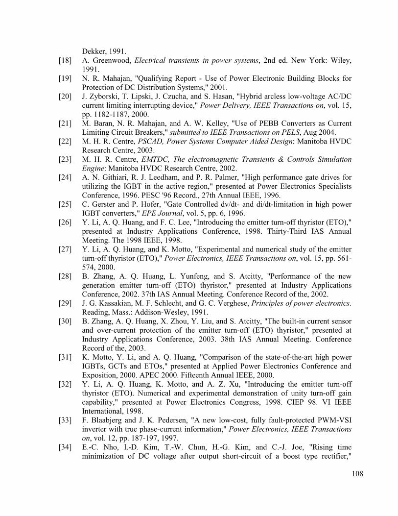
(TCC). Usually a TCC curve is plotted on log-log graph paper. The curve is produced from
time-current tests. They are performed with constant current applied to the fuse, in an
ambient temperature between 20 °C and 30 °C, with the fuse carrying no initial current. The
typical shape of a fuse’s melting TCC is shown in Figure 69(a). A single graph, such as the
one shown in Figure 69(a) represents curves for many different fuse elements (10E-450E in
the graph). The severing of a fuse element is caused by predominantly thermal, rather than
mechanical means, so there is virtually no limit on how short the melting time can be. This
very fast operation (melting) of a fuse at very high currents tends to be a distinguishing
characteristic of fuses compared to most other protective devices.
After the fuse element melts, the fuse must interrupt the current (which continues to flow
112
through an arc). After interruption, the fuse must withstand any immediate TRV condition
and the subsequent steady-state recovery voltage. When a fuse melts, there will always be
some period of arcing before the current is interrupted. The melting time is added to this
arcing period to obtain the total-clearing time. Total-clearing TCC curves are drawn to
present this information.
Typical performance data that is available from a manufacturer given in terms of 3 graphs.
TC characteristics: The TC curves are available in 2 forms: minimum melting curve and
total (or maximum) clearing time curve. These 2 curves represent the clearing times that
might be expected for a given current. Typical TC curves are shown in Figure 69(a) and
Figure 69(b).
The minimum melting curve is an average melting time measured in low voltage tests where
arcing does not occur. Thus, for a given current value, the time for the fuse to open the circuit
represents the melting time, which must fall within the tolerance given by the standards.
The second curve provides a measure of the total time to clear the circuit at a given current,
including the melting time and the arcing time.
The total clearing curve should be used in coordinating against the minimum melting
characteristics of a larger fuse, located towards the power source. Similarly, the minimum
melting curve should be used in coordinating with the total clearing of smaller fuses, located
on the load side.
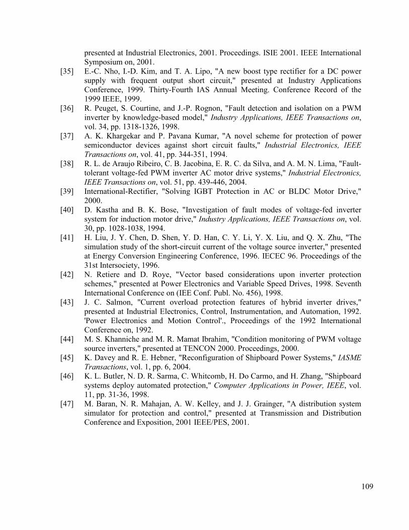
Cut-Off current characteristics: Figure 70, which plots the peak let through, or cut off
current, kA ( peak) versus prospective fault current, kA (RMS symmetrical), under the worst
case conditions of asymmetry that would normally be encountered. The point where the
individual characteristics depart from the line of peak symmetry would approximate to 10ms
time current point, i.e. the point where the fuse link starts to limit current (cut off) which
would be ½ cycle at 50 Hz.
113
(a) Minimum Melting TC Curve (b) Total Clearing TC Curve
Figure 69 : Fuse Characteristics
Figure 70 : Cut Off Current Characteristics
I2t characteristics: Figure 71, expresses the 2 most important quantities representative of
energy of fuse link. Firstly, the absolute minimum value of pre-arcing energy (min I2t),
which indicates the minimum energy in A2s that will result in the melting of the fuse
114
element. If this is exceeded then the fuse link element may be damaged thus altering the
characteristics. Secondly the total energy let-through (total I2t) which is a measure of the
maximum energy in A2s that the fuse link will let through at a particular voltage. It is
important to note that the operation of the fuse links under short circuit is dependent upon the
applied voltage and a significant reduction of total I2t can be seen with lower values of
applied voltages. Under no circumstance should fuse links be applied on systems above their
rated voltage.
Figure 71 : I2t Values
Now, with this basic understanding of the fuse, let us see how we can apply this for our
purpose.
In our application, the fuses are placed between after the generator breaker and the source
side of the rectifier PEBB. The main purpose of the fuse in out application is to provide
primary protection for the L-L faults and the 3-phase faults on the source side of the Rectifier
PEBB. These are the faults for which the RA cannot interrupt the fault current. The fuse also
provides backup protection for the RA.
The fuse we choose, therefore, should be fast enough so that it operates before the generator
protection. That is the fuse should properly coordinate with the upstream breaker –the
generator breaker. This ensures that the generator is tripped only to provide backup
protection for the fuses.
The fuse also provides short circuit backup protection to the RA. If the RA does not mal-
operate, it detects and interrupts faults in about 0.5ms. A typical fast action fuse, on the other
115
hand, takes few ms to 100ms to interrupt and isolate the faults (depending on fault current).
Therefore, if the RA mal-operates, a fast action fuse would automatically provide backup
protection. The choice of the fuse for providing backup protection to the RA, is therefore, not
critical and any fast action fuse can be chosen to provide backup protection.
Most high voltage fuse links are not designed to operate under extremely low over current
fault conditions, i.e. below the fuse links minimum breaking current. This is typically 2-3
times rated current. Fuse links of this type are normally equipped with a striker pin
mechanisms which are used to provide 3-phase tripping of the fuse switch.
The “E” rated fuses are general purpose current limiting fuses. They are capable of
interrupting currents that cause the fusible element to melt in 1 hour to the fuse links rated
interrupting current. The E rated fuses melt in 60mins at 220 to 264% of E rating, for
example a 200 E rated fuse must melt in 60mins for an applied current of 440 to 528 A.
These general purpose current limiting fuses are not applied as overload protection devices.
This type of fuse provides reliable protection above approximately 2.2 times the continuous
rated full load current. Transient currents of duration approaching fuse melting time may
physically damage the fuse element and cause a change in the melting characteristics.
Therefore when selecting such “E” rated fuse unit, we should allow proper allowance for
such expected short term transient conditions.
For our application, the current rating considerations for the choice of a fuse are
1. The normal rated current of the device to be protected is ~450A (RMS)
2. The startup current (due to initial capacitor charging via rectifier PEBB) is of the
order of 1kA (RMS) for about 5-10 milliseconds (<0.0ms).
3. The fault currents level is of the order 9-10kA for faults after source inductor and it is
of the order of to 30kA for faults before source inductor. The fuse is required to
operate for both these faults.
With these considerations in mind, a 500E type fuse with the rated current of 450A is
appropriate. An EJO-1 type 9F62 fuse from General Electric meets these requirements and
116
has been selected for the prototype SES.
To employ a fuse in the prototype system simulation, a fuse model was developed by the
author in PSCAD. Time-current fuse characteristics of the chosen fuse were entered into the
simulation as interpolated lookup tables. The energy required to melt and to clear at different
current level is also calculated and entered as interpolated lookup table. During the time
domain simulation, for a given value of current through the fuse, the energy dissipated in the
fuse is calculated at every instant. If this calculated energy (to melt and clear) exceeds the
energy required (to melt and clear) obtained from the lookup tables, then it implies that the
fuse has melted and cleared. As a confirmation, the time of operation of the simulated fuse is
matched with the time current curves from the specification sheets. Note that the developed
model does not include arcing, as modeling the arc would not enhance the simulations under
consideration.
Simulation results for one of the faults have been shown in “Rectifier Fuse for Rectifier AC
Zone” on page 42.
117
Appendix B Buck Converter Design Considerations
For the Buck Converter Agent to provide effective and comprehensive protection for the
faults shown in Figure 46, some important design choices have to be made. The main issues
that need attention are (i) Isolation transformer turn ratio, (ii) Device ratings, (iii) Switching
pattern function, (iv) Topology based on the switching pattern chosen, (v) Input inductor
values and (vi) Crowbar selections.
The most important issue, from protection perspective, is the turn ratio of the isolation
transformer. The main function of the isolation transformer is to provide isolation between
primary and the secondary sides of the buck converter. For the buck converter, therefore, the
typical turn ratio is 1:1. For achieving higher level of bucking action, a higher turn ratio can
be used. A higher turn ratio will lower the current in the CSDs of the source side or the BCIS
devices during the normal operation of the buck converter. At rated values of output current,
we can choose ETOs of the BCIS to be of a lower current rating. Therefore, a higher turn
ratio provides an advantage, as under normal operation, the I2R losses will be lower in the
BCIS devices.
Choosing devices with lower “normal current rating” will also lower the “maximum current
ratings”. This implies that for a given fault condition, the fault current will require a much
shorter time to exceed the maximum current rating of the low rated devices than if higher
rated devices were chosen. This in turn means that, when a higher turn ratio of the isolation
transformer is chosen, the BCA has shorter time to detect, identify and protect against faults.
Therefore, the BCA has to be faster, which can make the protection task of the BCA much
harder.
Therefore, various scenarios of different turn ratio were simulated. Different values of turn
ratio of the isolation transformer was chosen (8kV:8kV, 8kV:4kV, 8kV:2kV, 8kV:1.6kV and
8kV:1kV). For these scenarios, many parameters were observed, such as maximum allowable
current through ETOs, maximum current through the diodes of BCRS, typical duty ratio,
input current ripple, output voltage ripple, rise time of fault current, time for the buck
converter to completely shut-down (end-time for freewheeling of BCRS diodes), current
through ETOs during normal operation, losses in the buck converter. It was found that a 5:1
118
turn ratio, 8kV:1.6kV was suitable for normal operation and during protection. Devices
chosen with such a duty ratio allows enough time for the BCA to detect, identify and protect
the buck converter effectively. Therefore, a 5:1 turn ratio was chosen for the isolation
transformer.
With a turn ratio of 5:1, the current for normal operation of the Buck converter under full
load is about 200A. Since, typically the threshold of the protective devices is set to 2.5x the
normal rated current, the threshold of the BCA, to detect the faults, is set to 0.5kA. The
SLAP which provides backup protection to the BCA is set to 1kA, to achieve proper
coordination as described earlier. Therefore the CSDs (ETOs) of the BCIS are chosen to be
just higher than this with a rating of 1.1kA. The choice of such devices ensures that the BCA
has enough time to detect and identify the different faults.
The choice of the switching pattern function for the buck converter has three options [29].
First option is to turn off all the switches, the second option is to turn off S1 and S3 and the
third option is to turn off S2 and S4 as shown in Figure 45. The second and third options are
functionally indistinguishable.
The first option of turning off all the switches is employed here since with this switching
pattern, the switches of the BCIS carry only unipolar current. Due to this, the switches of the
BCIS can be realized by ETOs without an anti-parallel diode. This topological change is
important from protection perspective as with this modified topology, the Buck Converter
can provide protection and isolation for faults, by turning off all the CSDs (ETOs) of the
BCIS. By turning off all the switches of the BCIS, the magnetizing current is not chopped
off; it in forced to flow through the secondary winding and freewheeled through the diodes of
the BCRS. Therefore, this prevents any excessive voltages.
Note that another advantage results from the choice of this switching pattern. When all the
switches are off, the voltage is shared equally (3.5kV) between switches of same leg (S1, S4)
and (S2, S3), thereby reducing the voltage stress on the devices.
Another issue is the choice of Lin. A larger Lin aids in limiting the rate of rise of fault current,
while at the same time during turn-off of the current, a larger Lin will cause a higher voltage
119
rise ( =Lin*di/dt). Therefore, Lin should be chosen such that it provides enough time for the
BCA to detect the fault and at the same time does not cause an excessive over voltage.
The last important issue is the crowbar selection. As discussed in paragraph (c) of section
3.6. A crowbar device is connected from the positive bus to the negative bus at the input of
the Buck Converter. The device is a thyristor or a silicon-controlled rectifier (SCR) which is
normally OFF. When the failure of SLAP of the buck converter is detected, the thyristor or
the SCR is turned ON. The thyristor or the SCR must be chosen such that it has surge current
rating equal to or greater than the fault current level of the source side of the buck converter
for 1ms ( Rectifiers detect and interrupt the fault in about 0.5 ms).
120
Appendix C System Diagrams
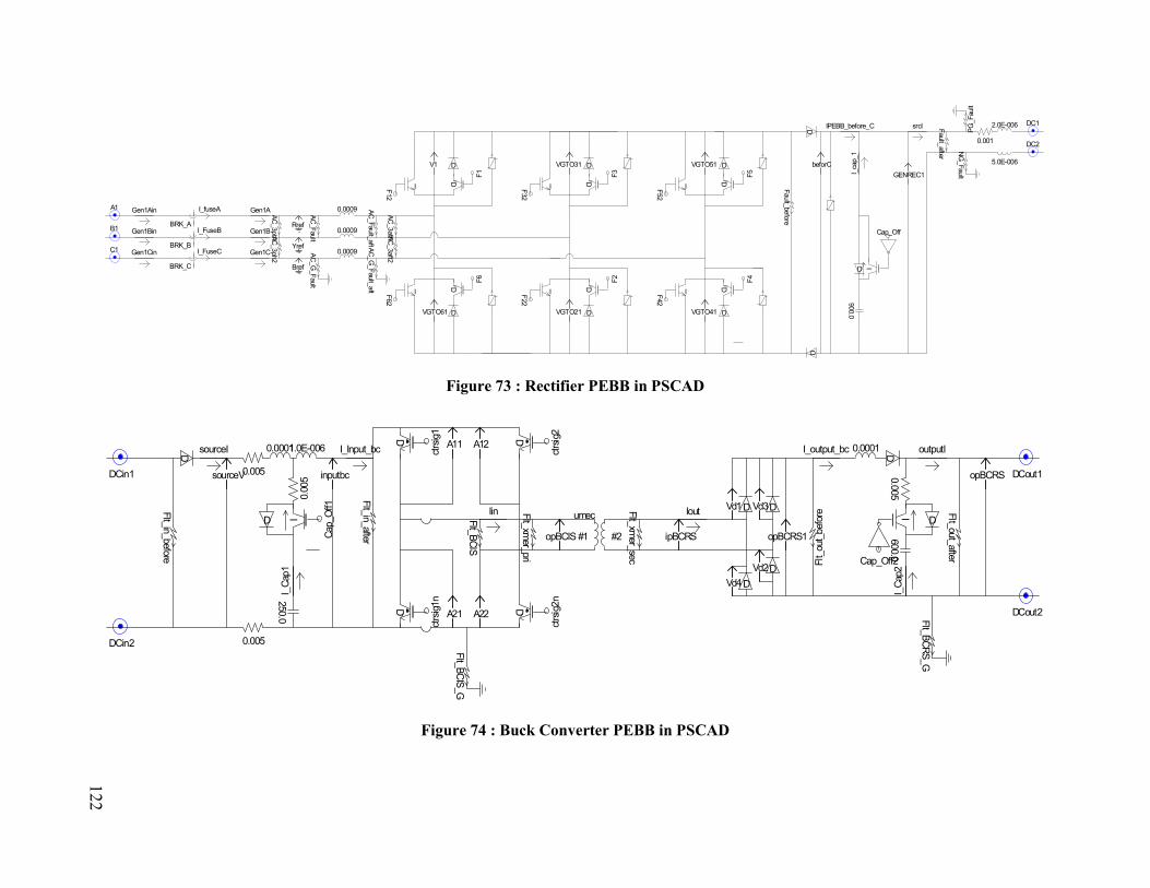
The PSCAD simulation diagram for the prototype system is shown in Figure 72. Blocks R1
and R2 represent the Rectifier PEBBs. The blocks B1, B2 and B3 represent the buck
converter PEBBs. The block, Iin1 represents the three-phase inverter.
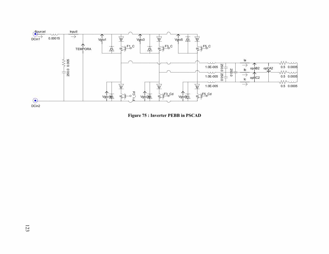
The simulation circuit for the rectifier PEBB is shown in Figure 73, the buck converter is
shown in Figure 74 and the circuit of the three-phase inverter is shown in Figure 75.