White Paper
Copyright © 2016 ARM Limited or its affiliates. All rights reserved.
Page 1 of 12
System Validation at ARM
Enabling our Partners to Build
Better Systems
M.S.Hrishikesh
Madhusudhan Rajagopalan
Sujatha Sriram
Rashmin Mantri
April 2016
White Paper
Copyright © 2016 ARM Limited or its affiliates. All rights reserved.
Page 2 of 12
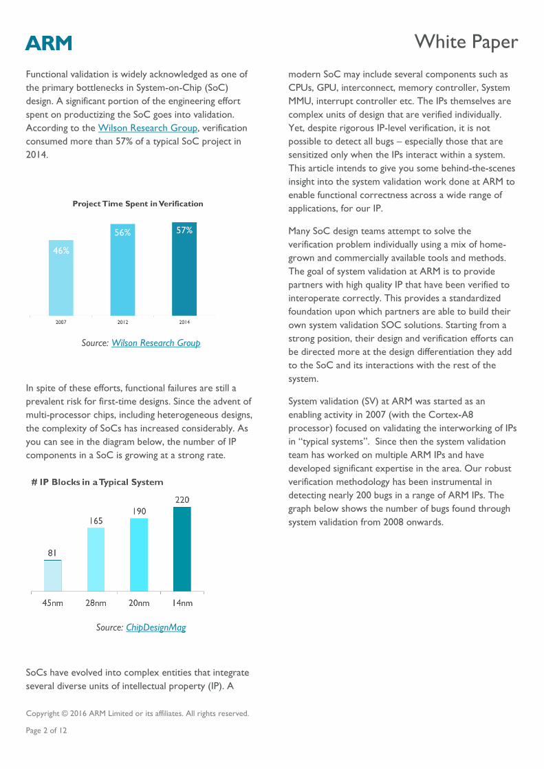
Functional validation is widely acknowledged as one of
the primary bottlenecks in System-on-Chip (SoC)
design. A significant portion of the engineering effort
spent on productizing the SoC goes into validation.
According to the Wilson Research Group, verification
consumed more than 57% of a typical SoC project in
2014.
Source: Wilson Research Group
In spite of these efforts, functional failures are still a
prevalent risk for first-time designs. Since the advent of
multi-processor chips, including heterogeneous designs,
the complexity of SoCs has increased considerably. As
you can see in the diagram below, the number of IP
components in a SoC is growing at a strong rate.
Source: ChipDesignMag
SoCs have evolved into complex entities that integrate
several diverse units of intellectual property (IP). A
modern SoC may include several components such as
CPUs, GPU, interconnect, memory controller, System
MMU, interrupt controller etc. The IPs themselves are
complex units of design that are verified individually.
Yet, despite rigorous IP-level verification, it is not
possible to detect all bugs – especially those that are
sensitized only when the IPs interact within a system.
This article intends to give you some behind-the-scenes
insight into the system validation work done at ARM to
enable functional correctness across a wide range of
applications, for our IP.
Many SoC design teams attempt to solve the
verification problem individually using a mix of home-
grown and commercially available tools and methods.
The goal of system validation at ARM is to provide
partners with high quality IP that have been verified to
interoperate correctly. This provides a standardized
foundation upon which partners are able to build their
own system validation SOC solutions. Starting from a
strong position, their design and verification efforts can
be directed more at the design differentiation they add
to the SoC and its interactions with the rest of the
system.
System validation (SV) at ARM was started as an
enabling activity in 2007 (with the Cortex-A8
processor) focused on validating the interworking of IPs
in “typical systems”. Since then the system validation
team has worked on multiple ARM IPs and have
developed significant expertise in the area. Our robust
verification methodology has been instrumental in
detecting nearly 200 bugs in a range of ARM IPs. The
graph below shows the number of bugs found through
system validation from 2008 onwards.
White Paper
Copyright © 2016 ARM Limited or its affiliates. All rights reserved.
Page 3 of 12
At the outset the validation flow was still getting set up
and expertise was being developed. Over time the
validation process has matured; tools have become
more precise, and IP designs are now placed into the SV
workflow much earlier in the verification cycle. This is
reflected by the increase in the number of bugs found
from 2013.
Verification at ARM: Early
and Often
The verification flow at ARM is similar to what is widely
practiced in the industry. Verification of designs starts
early and at the granularity of units, which combine to
form a stand-alone IP. During the entire verification
cycle it is at unit-level when engineers have the greatest
amount of visibility into the design. Individual signals
that would otherwise be deep within the design may be
probed or set to desired values to aid validation. Once
unit-level verification has reached a degree of maturity,
the units are combined to form a complete IP (e.g. a
CPU). Only then can IP-level verification of the IP
commence. For CPUs this is very often the first time
assembly program level testing can begin. Most of the
testing until this point is by toggling individual
wires/signals. At IP level the tests are written in
assembly language. The processor fetches instructions
from memory (simulated), decodes them executes etc.
Once IP-level verification reaches some stability
multiple IPs are combined into a system and the system
validation effort begins.
IPs from ARM go through multiple milestones during
their design-verification cycle that reflect their
functional completeness and correctness. Of these,
Alpha and Beta milestones are internal quality
milestones. LAC (Limited Access) represents the
milestone after which lead partners get access to the IP.
This is followed by EAC (Early Access), which
0
10
20
30
40
50
60
70
2008 2009 2010 2011 2012 2013 2014 2015
Bu
gs
White Paper
Copyright © 2016 ARM Limited or its affiliates. All rights reserved.
Page 4 of 12
represents the point after which the IP is ready to be
fabricated for obtaining engineering samples and testing.
By the REL (Release) milestone the IP has gone through
rigorous testing and is ready for mass production.
At ARM, system validation of IPs begin when they are
usually between Alpha and Beta quality. By this phase of
the design cycle the IPs have already been subjected to
a significant amount of testing and most low level bugs
have already been found. Stimulus has to be carefully
crafted so that the internal state of the micro-
architecture of each IP is stressed to the utmost. The
stimulus is provided by either assembly code or by
using specially designed verification IPs integrated into
the system. ARM uses a combination of both methods.
Many of these bugs could result in severe malfunctions
in the end product if they were left undetected. Based
on past experience ARM estimates these types of bugs
to take between 1-2 peta cycles of verification to
discover and 4-7 man months of debug effort. In many
cases, a delay that long would prove fatal to a chip’s
opportunity to hit its target window in the market.
Catching them early enough in the design cycle is
critical to ensure the foundations in the IP are stable,
before they go on to being integrated as part of a SoC.
The majority of bugs at system level (>60%) are found
between pre-Beta to LAC.
The goal of system validation is to ensure the
robustness of ARM IP based systems and ensure critical
bugs are discovered and fixed before the IP is released
to partners. SV provides partners with a standardized
platform with high quality of functional correctness,
saving them time and effort. Partners can now focus on
the design and verification of their own IPs and creating
SoCs for their target applications.
The remainder of this document describes ARM’s
system verification methodology and flow, including
how we build systems, the tools used in verification,
and the platforms used for validating the design.
A Multi-Layered Approach
to System Validation
The nature of ARM’s IP means it is used in a diverse
range of SoCs, from IoT devices to high end
smartphones to enterprise class products. Ensuring that
the technology does exactly what it is designed to do in
a consistent and reproducible manner is the key goal of
system validation, and the IP is robustly verified with
that in mind. In other words, the focus of verification is
IP, but in a realistic system context. Towards this end,
ARM tests IPs in a wide variety of realistic system
configurations that are called Kits.
A kit is defined as a “group of IPs” integrated together
for a specific target application segment (e.g. Mobile,
IoT, Infrastructure etc.). It typically includes the
complete range of IPs developed within ARM – CPUs,
interconnect, memory controller, system controller,
interrupt controller, debug logic, GPU and media
processing components.
A kit is further broken down into smaller components,
called Elements. Elements can be considered building
blocks for kits. It contains at least one major IP and
white space logic around it, though some of the
elements have several IP integrated in together.
These kits are designed to be representative of typical
SoCs with different applications. One result is that it
gives ARM a more complete picture of the challenges
faced by the ecosystem of integrating various IP
components to achieve a target system performance.
White Paper
Copyright © 2016 ARM Limited or its affiliates. All rights reserved.
Page 5 of 12
The system validation team uses a combination of
stimulus and test methodology to stress test kits.
Stimulus is primarily software tests that are run on the
CPUs in the system. The tests may be hand-created -
either assembly or high-level language – or generated
using Random Instruction Sequence - RIS tools, which
will be explained in the upcoming sections. In addition
to code running on CPUs, a set of Verification IPs
(VIPs) are used to inject traffic into the system or to act
as observers.
In preparation for validation, a test plan is created for
every IP in the kit. Test planning captures various IP
configurations, features to be verified, scenarios that
will be covered, stimulus, interoperability consideration
with IPs, verification metrics, tracking mechanisms, and
various flows that will be a part of verification. Testing
of kits starts with simple stimulus that is gradually
ramped up to more complex stress cases and scenarios.
The testing performs various subsystem level
assessments such as performance verification, functional
verification, and power estimation. This whitepaper
discusses only functional verification. Reports
documenting reference data, namely the performance,
power, and functional quality, of selected kits are
published internally. (This document focuses on
functional aspects only and more on Performance and
Power related topics will be covered in subsequent
blogs)
The system validation team at ARM has established a
repeatable and automated kit development flow, which
allows us to build multiple kits for different segments.
ARM currently builds and validates about 25 kits
annually.
The mix of IPs, their internal configuration, and the
topology of the system are chosen to reflect the wide
range of end uses. The kits are tested on two primary
targets – emulation and FPGA. Typically testing starts
on the emulator and subsequently soak testing is done
on FPGA. On average every IP is subjected to:
5-6 trillion emulator cycles
2-3 peta FPGA cycles of system validation
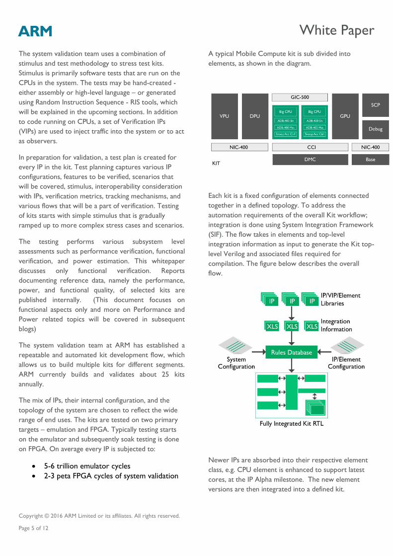
A typical Mobile Compute kit is sub divided into
elements, as shown in the diagram.
Each kit is a fixed configuration of elements connected
together in a defined topology. To address the
automation requirements of the overall Kit workflow;
integration is done using System Integration Framework
(SIF). The flow takes in elements and top-level
integration information as input to generate the Kit top-
level Verilog and associated files required for
compilation. The figure below describes the overall
flow.
Newer IPs are absorbed into their respective element
class, e.g. CPU element is enhanced to support latest
cores, at the IP Alpha milestone. The new element
versions are then integrated into a defined kit.
White Paper
Copyright © 2016 ARM Limited or its affiliates. All rights reserved.
Page 6 of 12
Kits are classified into two broad market segments –
mobile and infrastructure. Each segment is broken
down in to three sub-segments - high-end, volume,
wearable (in mobile) and optimized infrastructure, mid-
range infrastructure, and high-end infrastructure (in
infrastructure).
System Validation Tools
There are three primary tools used in System
validation, which are focused on areas like instruction
pipeline, IP level and system level memory system,
system coherency, interface level interoperability, etc.
Two of these tools are Random Instruction Sequence
(RIS) generators, referred to internally as Memory
Verification Generation Engine (MVGE) and System
Verification Engine (SVGE). RIS tools explore the
architecture and micro-architecture design space in an
automated fashion, attempting to trigger failures in the
design. They are more effective at covering the space
than hand written directed tests. These code
generators generate tests to explore different areas of
architecture and micro-architecture in an automated
fashion. The tests are multi-threaded assembly code,
comprised of random ARM and Thumb instructions,
designed to thoroughly exercise the functioning of
different portions of the implementation.
The third tool is a lightweight System Verification
Kernel (SVK) that can be used as a platform to develop
directed tests. The validation methodology uses a
combination of directed testing and random instruction
based automated testing. It supports basic memory
management, thread scheduling, and a subset of the
pthreads API, which allows users to develop
parameterized directed tests.
Such tests target very specific scenarios and are
typically used to test features that require an
orchestrated set up. Over the course of the past few
years we have developed a library of parameterized,
multi-threaded tests that are run on top of the kernel.
System Verification Kernel (SVK)
and System Verification
Generation Engine (SVGE)
SVK is a multi-processor aware bare metal kernel that
can support both multi-core and multi-cluster
platforms. The kernel provides a runtime environment
for multithreaded tests that includes thread scheduling,
exception handling, access protection, and memory
management.
The SVK kernel has a range of features to aid
verification. Some of them are listed below:
Virtual address (VA) to physical address
(PA) aliasing: SVK can create multiple virtual
address pointing to the same physical
address to provide aliasing
Tight loop irritator framework to target
denial-of-service bugs
System Test Suite (STS) that covers the
following areas: cache coherence, memory
attributes, atomics, memory ordering,
memory translation, power-down testing
etc.
The STS tests are parameterized and SVK can be
configured to randomize the parameters (within
allowed values) during each run. An example of such a
test is multi-threaded memory copy. The test consists
of multiple threads that copy data from one memory
location to another. In the process of reading and
writing data each thread will cause that data to be
loaded into the CPU’s cache. The data accessed by the
tests is organized so the same large set of cache lines
are accessed by all threads causing a lot of data
movement within the system.
SVGE is a RIS generator that runs as a thread in SVK. It
generates tests that primarily target the CPU pipeline
and its interaction with the memory system. To build an
SVGE image the user selects a weight configuration file
and any required macros. Using this information the
build system creates an executable image that can be
run on emulator, FPGA, or silicon. In the system
White Paper
Copyright © 2016 ARM Limited or its affiliates. All rights reserved.
Page 7 of 12
validation flow the images are run only on emulator and
FPGA.
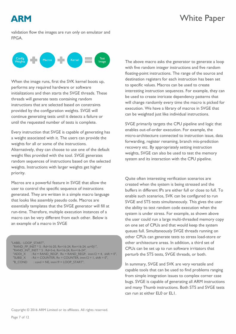
When the image runs, first the SVK kernel boots up,
performs any required hardware or software
initializations and then starts the SVGE threads. These
threads will generate tests containing random
instructions that are selected based on constraints
provided by the configuration weights. SVGE will
continue generating tests until it detects a failure or
until the requested number of tests is complete.
Every instruction that SVGE is capable of generating has
a weight associated with it. The users can provide the
weights for all or some of the instructions.
Alternatively, they can choose to use one of the default
weight files provided with the tool. SVGE generates
random sequences of instructions based on the selected
weights. Instructions with larger weights get higher
priority.
Macros are a powerful feature in SVGE that allow the
user to control the specific sequence of instructions
generated. They are written in a simple macro language
that looks like assembly pseudo code. Macros are
essentially templates that the SVGE generator will fill at
run-time. Therefore, multiple execution instances of a
macro can be very different from each other. Below is
an example of a macro in SVGE
The above macro asks the generator to generate a loop
with five random integer instructions and five random
floating-point instructions. The range of the source and
destination registers for each instruction has been set
to specific values. Macros can be used to create
interesting instruction sequences. For example, they can
be used to create intricate dependency patterns that
will change randomly every time the macro is picked for
execution. We have a library of macros in SVGE that
can be weighted just like individual instructions.
SVGE primarily targets the CPU pipeline and logic that
enables out-of-order execution. For example, the
micro-architecture connected to instruction issue, data
forwarding, register renaming, branch mis-prediction
recovery etc. By appropriately setting instruction
weights, SVGE can also be used to test the memory
system and its interaction with the CPU pipeline.
Quite often interesting verification scenarios are
created when the system is being stressed and the
buffers in different IPs are either full or close to full. To
enable such scenarios, SVK can be configured to run
SVGE and STS tests simultaneously. This gives the user
the ability to test random code execution when the
system is under stress. For example, as shown above
the user could run a large multi-threaded memory copy
on one set of CPUs and that would keep the system
queues full. Simultaneously SVGE threads running on
other CPUs can generate tests to stress load-store or
other architecture areas. In addition, a third set of
CPUs can be set up to run software irritators that
perturb the STS tests, SVGE threads, or both.
In summary, SVGE and SVK are very versatile and
capable tools that can be used to find problems ranging
from simple integration issues to complex corner case
bugs. SVGE is capable of generating all ARM instructions
and many Thumb instructions. Both STS and SVGE tests
can run at either EL0 or EL1.
"LABEL : LOOP_START",
"RAND_FP_INST * 5 : Rd=16-20, Rn=16-24, Rm=16-24, sz=0|1",
"RAND_INT_INST * 5 : Rd=3-6, Rn=16-24, Rm=16-24", "ADDI_X : Rd = RAND_REGP, Rn = RAND_REGP, imm12 = 4, shift = 0",
"SUBSI_X : Rd = COUNTER, Rn = COUNTER, imm12 = 1, shift = 0",
"B_COND : cond = NE, imm19 = LOOP_START",
White Paper
Copyright © 2016 ARM Limited or its affiliates. All rights reserved.
Page 8 of 12
Memory Verification Generation
Engine
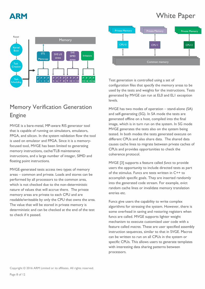
MVGE is a bare-metal, MP-aware RIS generator tool
that is capable of running on simulators, emulators,
FPGA, and silicon. In the system validation flow the tool
is used on emulator and FPGA. Since it is a memory-
focused tool, MVGE has been limited to generating
memory instructions, cache/TLB maintenance
instructions, and a large number of integer, SIMD and
floating point instructions.
MVGE-generated tests access two types of memory
areas – common and private. Loads and stores can be
performed by all processors to the common area,
which is not checked due to the non-deterministic
nature of values that will accrue there. The private
memory areas are private to each CPU and are
readable/writeable by only the CPU that owns the area.
The value that will be stored in private memory is
deterministic and can be checked at the end of the test
to check if it passed.
Test generation is controlled using a set of
configuration files that specify the memory areas to be
used by the tests and weights for the instructions. Tests
generated by MVGE can run at EL0 and EL1 exception
levels.
MVGE has two modes of operation – stand-alone (SA)
and self-generating (SG). In SA mode the tests are
generated offline on a host, compiled into the final
image, which is in turn run on the system. In SG mode
MVGE generates the tests also on the system being
tested. In both modes the tests generated execute on
different CPUs and also share data. The shared data
causes cache lines to migrate between private caches of
CPUs and provides opportunities to check the
coherence protocol.
MVGE [3] supports a feature called funcs to provide
users the opportunity to include directed tests as part
of the stimulus. Funcs are tests written in C++ to
accomplish specific goals. They are inserted randomly
into the generated code stream. For example, evict
random cache lines or invalidate memory translation
entries etc.
Funcs give users the capability to write complex
algorithms for stressing the system. However, there is
some overhead in saving and restoring registers when
funcs are called. MVGE supports lighter weight
mechanism to execute customized user code with a
feature called macros. These are user specified assembly
instruction sequences, similar to that in SVGE. Macros
can be written to run on all CPUs in the system or
specific CPUs. This allows users to generate templates
with interesting data sharing patterns between
processors.
White Paper
Copyright © 2016 ARM Limited or its affiliates. All rights reserved.
Page 9 of 12
Methodology
In order to stress test IP at the system level a more
random approach is used rather than a directed
approach. This enables ARM to cover a range of
scenarios, stimulate multiple timing conditions and
create complex events. To this end, Kits support
various verification-friendly features like changing the
clock ratios at different interfaces, enabling error
injectors, stubbing out components that are not
required for a given feature verification etc. Bus clock
ratios at various interfaces in the system like CPU,
interconnect and dynamic memory controller can be
changed to stimulate realistic system clocking
conditions. Random weighted delays can be added on
the AXI bus using the WRDM VIP. It generates delays
on Read and Write response channels based on these
values. This VIP mimics multiple bus timing conditions
between any two AXI interfaces in the system.
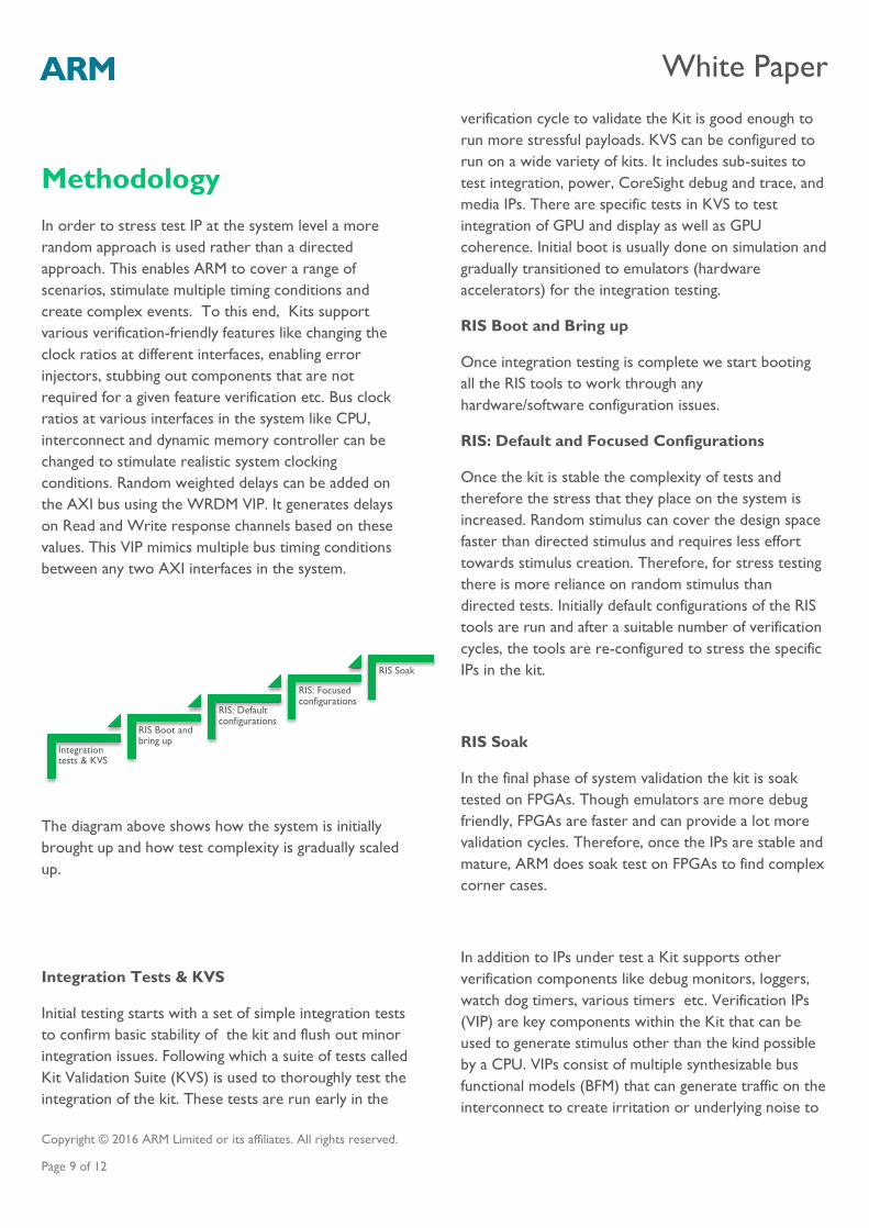
The diagram above shows how the system is initially
brought up and how test complexity is gradually scaled
up.
Integration Tests & KVS
Initial testing starts with a set of simple integration tests
to confirm basic stability of the kit and flush out minor
integration issues. Following which a suite of tests called
Kit Validation Suite (KVS) is used to thoroughly test the
integration of the kit. These tests are run early in the
verification cycle to validate the Kit is good enough to
run more stressful payloads. KVS can be configured to
run on a wide variety of kits. It includes sub-suites to
test integration, power, CoreSight debug and trace, and
media IPs. There are specific tests in KVS to test
integration of GPU and display as well as GPU
coherence. Initial boot is usually done on simulation and
gradually transitioned to emulators (hardware
accelerators) for the integration testing.
RIS Boot and Bring up
Once integration testing is complete we start booting
all the RIS tools to work through any
hardware/software configuration issues.
RIS: Default and Focused Configurations
Once the kit is stable the complexity of tests and
therefore the stress that they place on the system is
increased. Random stimulus can cover the design space
faster than directed stimulus and requires less effort
towards stimulus creation. Therefore, for stress testing
there is more reliance on random stimulus than
directed tests. Initially default configurations of the RIS
tools are run and after a suitable number of verification
cycles, the tools are re-configured to stress the specific
IPs in the kit.
RIS Soak
In the final phase of system validation the kit is soak
tested on FPGAs. Though emulators are more debug
friendly, FPGAs are faster and can provide a lot more
validation cycles. Therefore, once the IPs are stable and
mature, ARM does soak test on FPGAs to find complex
corner cases.
In addition to IPs under test a Kit supports other
verification components like debug monitors, loggers,
watch dog timers, various timers etc. Verification IPs
(VIP) are key components within the Kit that can be
used to generate stimulus other than the kind possible
by a CPU. VIPs consist of multiple synthesizable bus
functional models (BFM) that can generate traffic on the
interconnect to create irritation or underlying noise to
Integration tests & KVS
RIS Boot and bring up
RIS: Default configurations
RIS: Focused configurations
RIS Soak
White Paper
Copyright © 2016 ARM Limited or its affiliates. All rights reserved.
Page 10 of 12
keep the system busy. The BFMs represent traffic from
other potential IPs that can be put in the system. Other
VIPs act as observers that check architectural
specifications such ordering of memory transactions.
The figure above shows an example mobile kit and
describes where the VIPs are placed in the system.
Hardware irritators that generate traffic on the
system buses like AXI, ACE-lite, and CHI traffic
generator are protocol compliant. They can generate a
multitude of traffic patterns stimulating various
memory system timing conditions. The traffic patterns
mimic the kind of pattern that may be generated by
other IPs that may be connected to the system. There
are custom hardware irritators for generating traffic to
the accelerator coherency port of the CPU and
message signalled interrupts (MSI) on to the system bus.
Error injectors play a key part to test and check the
ECC logic in different IPs when the system is placed
under different traffic conditions.
Clock and power gating BFM and irritators emulate
the behaviour of multiple representative power and
clock controller behaviour thus ensuring good coverage
for power state sequencing and clock gating.
In addition to the above, a third-party PCIe IP is used in
the system to ensure that memory and bus ordering
rules are complied with. Synthesisable assertions are
used as a technique to catch IP bugs. Protocol checkers
are also used to ensure that when various IP are put
together with standard buses connected they adhere to
protocol . Power state of IPs and dynamic clock gating
are a key features that needs special attention and
hence power aware verification flow is used to cover
various power states. As the goal of system validation is
stress testing at a system level, statistical coverage of
interesting events is instrumented to get a measure of
stress testing. In addition to stress testing we also test
the system by booting a full operating system (e.g.
Linux) and running compliance tests on the system.
Metrics, Tracking,
Coverage, and Milestone
Closure
The number of validation cycles run for every Kit is one
of the metrics that is tracked to ensure the target
number of validation cycles has been met. This is
especially useful to ensure the soak-testing cycle target
has been met, increasing the confidence of the quality of
the IP in various applications. In addition to that we
quantify and track coverage using a statistical coverage
method to ensure the full design including potential
corner cases have been exercised sufficiently.
An automatically updated dashboard provides a good
view of the progress of planned verification tasks for
every milestone. It shows the number of cycles run on
emulation and FPGA and the number of tasks
completed. This information along with the pass rate of
tests is an indicator of the quality of IP and system
stability.
We use coverage metrics to evaluate if the entire
design is being well exercised by the stimulus and to get
an estimate of how intensely each area is covered. A list
of interesting system level events are collected across
regressions and statistically analysed. The analysis is
used as a feedback to enhance test stimulus including
configuration changes, changes in RIS generators, and
VIPs.
White Paper
Copyright © 2016 ARM Limited or its affiliates. All rights reserved.
Page 11 of 12
For example, on top of the >10,000 hours of validation
run time done on each core model, the latest version of
the ARM Juno test chip was subjected to an additional
6,130 hours of system validation run time. This is the
equivalent of 8 and a half months of testing. This gives a
unique perspective into corner cases within the system
that makes ARM better able to support partners who
are attempting to debug issues within their own design.
Furthermore, the bugs that are found during the
validation process are then fed back into the IP design
teams who use the information to improve the quality
of the IP at each release milestone, as well as guide
next-generation products.
Summary
System complexity has increased in line with SoC
performance capabilities, causing a significant growth in
the amount of time and money spent on validation.
ARM verifies its IP for interoperability before it is
released to partners to make sure it is suitable for a
wide range of applications. ARM’s IP teams are
continuously designing at the leading edge, and are
helped by the system validation team to ensure they
work together in the systems our partners are building.
Frank Schirrmeister of Cadence Design Systems cites.
“As an ARM ecosystem partner, Cadence relies on pre-
verified ARM cores and subsystems that can be easily
integrated into the designs that we use to validate our tool
interoperability. ARM’s software-driven verification approach
reflects the industry’s shift toward the portable stimulus
specification and allows us to validate the integration and
interoperability of ARM cores and subsystems on all
Cadence System Development Suite engines, including
simulation, emulation and FPGA-based prototyping engines.”
Due to the wide variety of applications that the ARM
partnership designs for, it is necessary to ensure our IP
is functional in many different systems. The multi-stage
approach to system validation at ARM gives our
partners the peace of mind that they can rely on our IP.
Over time the validation methodology has evolved into
one that tests several system components and stresses
most IPs in the system. In the future we have plans to
extend and further improve our test methods to ensure
an even higher standard of excellence across ARM IP.
References
1. Prabhat Mishra and Nikil Dutt , “Functional
Coverage Driven Test Generation for
Validation of Pipelined Processors” ,
Proceedings of the conference on Design,
Automation, and Test in Europe – Volume 2.
2005
2. W. Wolf, A. A. Jerraya, and G. Martin,
“Multiprocessor System-on-Chip (MPSoC)
Technology”, IEEE Transactions on Computer-
Aided Design of Integrated Circuits and
Systems, Vol. 27(Iss. 10): pages 1701-1713,
2008.
3. Shajid Thiruvathodi and Deepak Yeggina, “A
Random Instruction Sequence Generator For
ARM Based Systems”, Microprocessor Test and
Verification Workshop, 2014
4. Deepak Venkatesan and Pradeep Nagarajan, “A
Case Study of Multiprocessor Bugs Found Using
RIS Generators and Memory Usage
Techniques,” Microprocessor Test and
Verification Workshop, 2014
5. Design for verification methodology allows
silicon success. EETIMES, (16500856), 2003
Trademarks The trademarks featured in this document are
registered and/or unregistered trademarks of ARM
Limited (or its subsidiaries) in the EU and/or elsewhere.
All rights reserved. All other marks featured may be
trademarks of their respective owners. For more
information, visit arm.com/about/trademarks.
White Paper
Copyright © 2016 ARM Limited or its affiliates. All rights reserved.
Page 12 of 12


![INDEX [] · 5 Saturated Fatty Acid (SFA): SFAs are widely used in packaged foods including cookies, crackers, and snack chips. When consumed in excess of the recommended (limit less](https://static.documents.pub/doc/80x56/5ed434c5a9596d397405e036/index-5-saturated-fatty-acid-sfa-sfas-are-widely-used-in-packaged-foods-including.jpg)
