Rochester Institute of Technology Rochester Institute of Technology RIT Scholar Works RIT Scholar Works Theses 12-2017 SystemVerilog Verification of Wishbone-Compliant Serial SystemVerilog Verification of Wishbone-Compliant Serial Peripheral Interface Peripheral Interface Avinash Srinivasan [email protected]Follow this and additional works at: https://scholarworks.rit.edu/theses Recommended Citation Recommended Citation Srinivasan, Avinash, "SystemVerilog Verification of Wishbone-Compliant Serial Peripheral Interface" (2017). Thesis. Rochester Institute of Technology. Accessed from This Master's Project is brought to you for free and open access by RIT Scholar Works. It has been accepted for inclusion in Theses by an authorized administrator of RIT Scholar Works. For more information, please contact [email protected].
Transcript
Rochester Institute of Technology Rochester Institute of Technology
RIT Scholar Works RIT Scholar Works
Theses
12-2017
SystemVerilog Verification of Wishbone-Compliant Serial SystemVerilog Verification of Wishbone-Compliant Serial
Follow this and additional works at: https://scholarworks.rit.edu/theses
Recommended Citation Recommended Citation Srinivasan, Avinash, "SystemVerilog Verification of Wishbone-Compliant Serial Peripheral Interface" (2017). Thesis. Rochester Institute of Technology. Accessed from
This Master's Project is brought to you for free and open access by RIT Scholar Works. It has been accepted for inclusion in Theses by an authorized administrator of RIT Scholar Works. For more information, please contact [email protected].
SystemVerilog Verification Of Wishbone-Compliant Serial PeripheralInterface
byAvinash Srinivasan
Graduate PaperSubmitted in partial fulfillment
of the requirements for the degree ofMaster of Science
in Electrical Engineering
Approved by:
Mr. Mark A. Indovina, LecturerGraduate Research Advisor, Department of Electrical and Microelectronic Engineering
Dr. Sohail A. Dianat, ProfessorDepartment Head, Department of Electrical and Microelectronic Engineering
Department of Electrical and Microelectronic EngineeringKate Gleason College of Engineering
Rochester Institute of TechnologyRochester, New York
December, 2017
I dedicate my work to my mentor Professor Mark Indovina, my father SrinivasanKrishnarao, mother Ratna Srinivasan, brother Abhishek, sister-in-law Swathi and friends
for their support during my thesis.
Declaration
I hereby declare that except where specific reference is made to the work of others, that allcontent of this Graduate Paper is original and have not been submitted in whole or in partfor consideration for any other degree or qualification in this, or any other University. Thisresearch project is the result of my own work and includes nothing which is the outcomeof work done in collaboration, except where specifically indicated in the text.
Avinash SrinivasanDecember 19, 2017
Acknowledgements
I wholeheartedly thank my graduate advisor and mentor Professor Mark Indovina forhis continued support, feedback, encouragement and guidance through out my graduatecareer and research. I also thank Dr. Dorin Patru and Dr. Jayanthi Venkataraman fortheir support and guidance through out my graduate career.
Abstract
Synchronous serial interfaces provide economical on-board communication between theprocessor, digital to analog and analog to digital converters, memory, and other build-ing blocks on the chip. A number of Integrated Circuit (IC) manufacturers develop andproduce components that are compatible with serial interfaces. The common serial inter-faces include Serial Peripheral Interface (SPI), Inter-Integrated Circuit (I2C), UniversalAsynchronous Receiver Transmitter (UART), and Universal Serial Bus (USB). SPI iswidely used and advantageous over other serial interfaces due to its features of simplicity,low cost, clock synchronous, and non-interrupting high-speed data transfer rate. SPI is thecore controller of the design. An open source hardware computer bus Wishbone is selectedas the host controller enabling parallel data exchange for faster communication. Boththe hardware buses employ a master-slave configuration which makes the bus-interfacingeasier.
This research presents a verification environment using SystemVerilog for the SPI Mas-ter device. An existing design from Open Cores is re-used, described as per latest speci-fications in Verilog at the Register Transfer Level (RTL) and is in conformity with thedesign-reuse methodology. This paper provides an understanding of the verification, lay-ered test benches, Object-Oriented Technology (OOT), SystemVerilog, SPI features, SPIadvantages, disadvantages, and applications, SPI data transmission and transfer formats,SPI registers, SPI sub-system and Wishbone-SPI architecture, and the test bench devel-opment methodology. The focus is to understand how OOT and SystemVerilog improveproductivity and functional coverage in a verification environment by the use of differentconstructs, constrained-random techniques, coverage, and assertions. A test bench wasdeveloped to verify the SPI master core. Testbench components include a random trans-action generator, a Wishbone driver, an SPI master as the design under test, a receiveras the SPI slave, a monitor with tasks to monitor the host and the core, test cases, and ascoreboard to record metrics, assertions and store expected and actual data.
An Application Specific Integrated Circuit (ASIC) is is a special purpose device designedfor a specific application and perform a specific function. A modern ASIC may includemicroprocessors or microcontrollers, memory and relevant building blocks on a single chipcalled a System-on-Chip (SoC). The presence of a microprocessor or microcontroller dis-tinguishes an ASIC as an SoC or a non-SoC. A mobile phone is a classic example of anembedded system which embeds a SoC. The mobile phone SoC includes a Microcontroller,a Digital Signal Processor (DSP), Memory, Peripherals, Direct Memory Access controller(DMA controller), Liquid Crystal Display controller (LCD controller) and a battery. AnSoC is always developed to provide better reliability, lower cost, lower area, lower power,better performance and to meet the technology advancements and product end-user re-quirements. An Embedded System or a SoC uses a microcontroller or a microprocessor forintelligent control mechanism, display drivers for displaying the content, memory for stor-age, data converters, remote input and output ports, and integrated circuits for communica-tion interfaces. The desired functionality is achieved when multiple components of the chipoperate, communicate and collaborate with each other. These components interact witheach other through communication controllers or interfaces. The interfaces may be serialor parallel depending on the transmission of data and are selected based on the protocolssupported by the components. A few interfaces include Serial Peripheral Interface (SPI),Inter-Integrated Circuit (I2C), Universal Asynchronous Receiver Transmitter (UART),Universal Serial Bus (USB), Ethernet, Bluetooth, WiFi, Avionics Full DupleX SwitchedEthernet (AFDX), Controller Area Network (CAN), Aeronautical Radio INC 429(ARINC 429), MILitary-STandarD-1553 (MIL-STD-1553). SPI, I2C, UART, andUSB are most common serial interfaces used.
2
SPI is advantageous over I2C and UART as the data exchange is synchronous to a clocksignal and is configured as a master-slave device. SPI master device is the core controller.An open source hardware computer bus Wishbone is the host controller to SPI and itenables parallel exchange of data with the processor. It is configured as a master-slave likethe SPI, which makes the interfacing easier. As a result, the core controller is a slave ofthe host controller. Motorola developed the SPI communication controller. It is a data-link and a De facto standard. Parallel data from the microprocessor or microcontrolleris transmitted through Wishbone to the SPI Master device. This data is serialized inbits with one bit being transmitted to the slave in a clock cycle. The slave acknowledgesthe master in a similar way. The transmission and reception of data between the SPImaster device and the SPI slave device happen simultaneously and the communication isfull duplex. SPI is a 3+-wire (typically 4), synchronous serial controller. The interfacesof SPI include Serial ClocK (SCK), Master In Slave Out (MISO), Master Out SlaveIn (MOSI) and an optional Slave Select (SS). Unlike Wishbone, SPI supports only asingle master and a multiple slave configuration. At any given instance, only the masterdevice can initiate a data frame transfer with only one slave device by generating the clocksignal through SCK and selecting the slave device through SS. The SPI master operatesas an 8-bit shift register. The SPI slave operates as an 8-bit shift register. The SPI masterand slave devices are tied together through the interfaces of the SPI. Ideally, the LeastSignificant Bit (LSB) of the master is transferred into the Most Significant Bit (MSB)of the slave through MOSI data line and the Most Significant Bit (MSB) of the slave istransferred into the Least Significant Bit (LSB) of the master through the MISO dataline. This two-way communication works similar to a 16-bit circular shift register. SCKsynchronizes the sampling and shifting of data on the MISO and MOSI by assigning theclock phase, clock polarity, and clock frequency.
SPI is widely used in the industry for its swift data transfer rates with a bit rate of halfthe clock rate and can operate at a speed of up to 1.1 Mbps. A flexible design methodologythat is used with semiconductor IP cores is the Wishbone Bus Interconnection. It enablesfaster design re-usability in the integration of the chip due to its simple, compact, andlogical IP core hardware interfaces requiring less number of logic gates. It enables paralleldata communication on a chip and is selected as the host controller to the SPI.
The design implementation of these hardware platforms can be carried out using Ver-ilog Hardware Description Language (Verilog HDL) or Very High-Speed IntegratedCircuit Hardware Description Language (VHDL). But Verilog or VHDL is not enough
3
for a complete verification of these platforms. The traditional approach of verificationis to functionally simulate the hardware, develop and emulate the software by transact-ing all the input combinations to the design under test and monitoring the expectedbehavior. This approach is time-consuming and poses a major threat to design andverification re-work. An automated system-level verification with re-usable and scal-able components is required to verify complex designs. A majority of the ElectronicDesign Automation (EDA) tool vendors use automated verification methodologies andObject-Oriented Technology (OOT). The automated verification methodologies includeSystemVerilog, Universal Verification Methodology (UVM), Verification MethodologyManual (VMM), Advanced Verification Manual (AVM), and Open Verification Manual(OVM) [6]. SystemVerilog is extensively used in verifying complex SoC designs due tohigher level abstractions and use of OOT. It combines specifications, design, simulation,verification and validation into a single language by improving the communication betweendesign and verification engineers aiding an efficient design and verification process. Three-fourths of the time in the product development life cycle is spent on verification and testing.Given adequate time and resources, direct testing is used to exploit features of verifica-tion environment. The increasing levels of design complexity force the usage of randomtests by automation in addition to certain directed tests to cover all the input combina-tions and achieve a 100% functional and code coverage metrics. Unlike traditional directedtesting, random tests start with the expected behavior and work backward to check theoutputs with automatically generated input stimulus through transaction generators. Averification environment is developed through a layered approach. The layered approachdivides the tasks into Signal, Functional, Command, Scenario and Test layers developedindependently. This environment is built upon a verification plan which describes the as-pects of the design to be verified, the techniques to be used and the creation of constrainedrandom tests. Code and Functional coverage metrics are captured to check all aspects ofthe verification plan. Functional coverage measures the test success rate to evaluate theperformance. Code Coverage measures the coding standards metrics.
A configurable and reusable verification environment to validate the Wishbone-compliantSPI core controller is developed using SystemVerilog. The test scenarios include differentcharacter lengths, reset condition, data transmission modes, interrupt checks and AutoSlave Select function. The constrained-random stimulus generator generates the transac-tions and the driver is in the form of Wishbone. The design under test is the SPI master.The receiver is the SPI slave. Monitors are used on the host-side and core-side to check
1.1 Research Goals 4
the actual data and the expected data. A scoreboard is used for temporary storage, andto capture the coverage metrics and assertions.
1.1 Research GoalsThe goal is to build a configurable and re-usable complex verification test bench thatvalidates the Wishbone-compliant SPI communication controller. A top-down design [7]and a layered verification approach are followed to achieve this goal. The objectives includeunderstanding the system requirements and specifications, Wishbone-SPI architecture, SPIregisters, SPI data transmission modes, the creation of a testbench environment, andanalysis of the data transmission.
1.2 ContributionsThe major contributions to the Wishbone-SPI Core communication controller include:
• Understanding the SPI sub-system architecture, Wishbone-SPI architecture, verifi-cation, Object-oriented Technology and SystemVerilog.
• Modifying existing designs of the Wishbone-SPI communication controller as per thelatest specifications.
• Developing the testbench components of the verification environment using Sys-temVerilog constructs, random stimulus, assertions, and coverage.
• Connecting the components of the verification environment to verify the transmissionof data for different character lengths and data transfer formats.
1.3 OrganizationThis paper has been organized in the following way:
• Chapter 2 focuses verification, strategies involved in creating a verification environ-ment, and benefits of layered approach.
• Chapter 3 describes the benefits of using object-oriented technology and SystemVer-ilog.
1.3 Organization 5
• Chapter 4 describes in detail the Serial Peripheral Interface, its salient features,advantages, disadvantages, applications, data transmission, registers, Wishbone, SPIsub-system, and Wishbone-SPI architecture.
• Chapter 5 outlines the developed verification environment, the testbench components,the testbench code methodology, and the testbench results.
• Chapter 6 concludes the paper by highlighting the possible scope of the possiblefuture work in this research.
Chapter 2
Verification
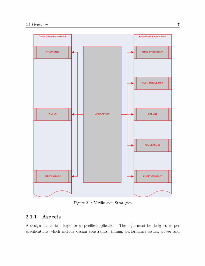
2.1 OverviewThe complexity of ASIC and SoC designs increases exponentially [8]. Verification of thesehardware platforms is highly essential as a bug in silicon can lead to increased costs. En-hanced verification strategies using directed and constrained random tests are required toensure successful design implementations. The process of demonstrating a design’s func-tional correctness is verification. The ultimate goal of verification is to minimize the costs,and achieve maximum code and functional coverage in a short span of time. Verificationdetermines incorrect specifications, misinterpretations, incorrect interactions between coresand identifying unexpected system behavior through strategies like functional verification,object-oriented analysis, assertions, and randomization. A verification environment canbe developed methodically by addressing concerns as to what aspects of the design has tobe verified and how should the design be verified. Fig. 2.1 shows the different strategiesinvolved in verification.
2.1 Overview 7
Figure 2.1: Verification Strategies
2.1.1 Aspects
A design has certain logic for a specific application. The logic must be designed as perspecifications which include design constraints, timing, performance issues, power and
2.1 Overview 8
area constraints. The following verification strategies define the aspects of the design tobe verified and are divided into functional, timing and performance.
2.1.1.1 Functional
It is a process of verifying the logic of the design under test that conforms to the speci-fications using a mathematical model. It is cumbersome due to the enormous test casespresent to verify the logic. It cannot be the only source of verification as it takes a lot oftime and effort. It is supported by logic simulation, formal verification, RTL verification,Gate and Netlist level verification and emulation.
2.1.1.2 Timing
It validates the path delays from the primary input to the primary output to ensure thatthese delays are neither too short nor too long. It validates the clock pulses to ensure thatthey are neither too wide nor too narrow and the pulse width is retained as required. Thisis a kind of an electrical rule check and uses static and dynamic timing analysis to verifythe timing constraints.
2.1.1.3 Performance
It determines whether a design meets the specified performance criteria. It may be per-formed in a hierarchical manner. For example, individual cells of the integrated circuitmay be tested against desired performance goals during the initial pass. Testing may thenproceed at the block level and finally at the full chip level for subsequent passes to meetperformance criterion.
2.1.2 Methods
The logic, timing, performance, and power constraints can be verified using simulations,emulations, formal methods, assertions, and co-verification of hardware and software. Thefollowing verification strategies support the above verification strategies and are selectedbased on the complexity of the design.
2.1 Overview 9
2.1.2.1 Simulation-based
It is the traditional approach which is still used to verify any design and is one of themajor components of the verification space. It requires the generation of input sequencesor vectors and derives the reference outputs. The input sequences generated can be directedinputs, random inputs and constrained random inputs. It is input-driven and requires thegeneration each and every data-point input to capture the system’s behavior. As a result,it generally requires a longer simulation time, especially for larger designs. This verificationhas to be supported by other verification strategies to achieve maximum functional andcode coverage.
2.1.2.2 Emulation-based
This technique needs a certain emulation system like an FPGA-based board. It can providea shorter verification cycle of the design and cannot be the only source of verification.The time and logic required to design a specific application must also include a boarddevelopment time.
2.1.2.3 Formal
Unlike the simulation-based technique, this verification starts by deciding the desired out-put behavior of the design under test. A formal checker approves or disproves the obtainedresults. It is output-driven and a collection of data points or properties generated by arandom stimulus generator are verified. As a result, missing an input space does not occur.It is the most widely used strategy for modern day SoCs but the main drawback is the useof extensive memory and a longer run-time. It consists of two approaches namely modelchecking and formal equivalence checking [9].
2.1.2.4 Semi-Formal
A handful of tool vendors consider adopting this strategy in verifying a design as it com-bines the simulation-based and formal verification. It achieves better results, and coveragemetrics with lesser verification time in the product development life cycle.
2.2 Verification Plan: A Layered Approach 10
2.1.2.5 Assertion-based
An assertion is the description of the property of a design as per the specifications. Asser-tions help in validating the design’s intended behavior. The benefits of an assertion-basedverification technique include improving the error detection for spotting simulation errors,improving the ability to debug effectively, improving the observability, usage in formal ver-ification and dynamic simulation-based and providing a correct functional coverage. Twotypes of assertions can be used and these include immediate and concurrent assertions[10][11].
2.1.2.6 Co-verification of Hardware and Software
It provides the facility of verifying the hardware and the software functionality of anapplication specific design simultaneously. It is required due to the complexity, and demandfor low cost and high volume consumer products. It requires a shorter time of verifyingthe complete design. It verifies the execution of the embedded system software accuratelyon the target embedded system hardware before the design is committed to fabrication.The simulation of the hardware logic behaves as the real hardware but it is actually anapplication software on a workstation. The benefits include an early access to the hardwaredesign for the software developers and presence of stimulus for hardware engineers [12, 13].
2.2 Verification Plan: A Layered ApproachThe goal of verification is to ensure that the device functions accurately and effectivelyas per the specifications and the expected behavior [14]. A verification plan is created toexplain different aspects of the design to be verified based on the specifications and thetechniques that are to be used to achieve the goal. The traditional approach is to generatethe stimulus, apply the stimulus to the design under test and capture the results, checkfor the correctness against specifications, and measure the progress. A flat testbench isdeveloped based on the plan, which wraps around the design under test. Different scenariosare created in the testbench which provide stimulus to the design to capture the results.These results are checked with the expected results from the testbench. The testbenchenvironment has different levels of abstraction, creates transactions and sequences whichhas to be later transformed to bit vectors [14]. As a result, modulating the flat testbenchprogrammed in Verilog into different layers and smaller chunks of logic makes it easier,
2.2 Verification Plan: A Layered Approach 11
efficient and maintainable. As a result, a layered testbench is developed and divided intosignal, command, functional and scenario layers [14].
The Signal Layer is the lowest level in the layered testbench. It holds the design andthe interface signals that connect it to the testbench.
The Command Layer is the next level which holds the driver to drive input trans-actions to design, monitor the transactions through checkers and assertions. The driverdrives the input transactions to the design from the stimulus generator through singlecommands. The design’s output drives the monitor to group them into commands byconsidering signal transitions. Assertions validate the signals integrity by considering thechanges in the signals and the changes across an entire command. Fig. 2.2 showcases thesignal and command layers of the environment.
Figure 2.2: Signal and Command Layers
The Functional Layer forms the next layer and is one of the key layers of the layeredtestbench. It consists of the agent or stimulus, scoreboard, and checkers. The agentreceives higher level transactions and splits them into individual transactions to be sent tothe driver and scoreboard. Scoreboard predicts the results of the occurred transactions.Checker is used to comparing the commands received from the monitor with the predictedresults from the scoreboard [14]. Fig. 2.3 showcases the environment with the functionallayer included.
2.2 Verification Plan: A Layered Approach 12
Figure 2.3: Functional, Signal and Command Layers
The Scenario Layer is primarily responsible for generating the test scenarios or testcases required to drive the Functional layer. Usually, constrained random values of differentparameters are generated by the scenario layer and is responsible for working of the otherlayers or steps in this verification testbench [14].
The scenario, command and functional layers form the testbench environment whichare depicted in Fig. 2.4.
2.2 Verification Plan: A Layered Approach 13
Figure 2.4: Scenario, Functional, Signal and Command Layers
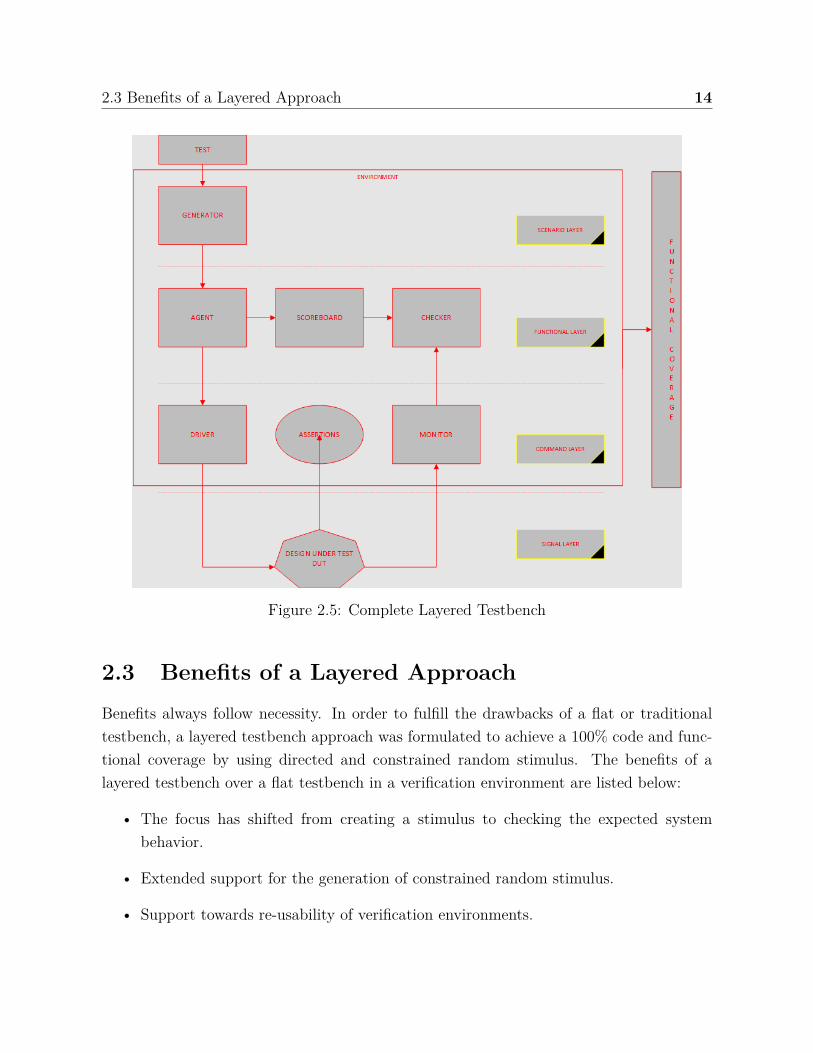
The Test Layer and the Functional Coverage Layer form the top layers of a testbenchenvironment. The top-level test only guides the efforts of other components of the testbenchand it contains the constraints to create the stimulus. Functional Coverage Layer onlymeasures the progress of all tests to check if all the verification plan requirements are met.Fig. 2.5 represents a complete Testbench Environment with all the layers included.
2.3 Benefits of a Layered Approach 14
Figure 2.5: Complete Layered Testbench
2.3 Benefits of a Layered ApproachBenefits always follow necessity. In order to fulfill the drawbacks of a flat or traditionaltestbench, a layered testbench approach was formulated to achieve a 100% code and func-tional coverage by using directed and constrained random stimulus. The benefits of alayered testbench over a flat testbench in a verification environment are listed below:
• The focus has shifted from creating a stimulus to checking the expected systembehavior.
• Extended support for the generation of constrained random stimulus.
• Support towards re-usability of verification environments.
2.3 Benefits of a Layered Approach 15
• Improving the code and functional coverage through constrained random stimulus.
• Reducing the tool integration time.
• Allows creating a flexible, adaptable and a scalable testbench environment to increasethe robustness of functional verification.
Chapter 3
SystemVerilog
3.1 Object-Oriented Technology
3.1.1 Overview
Object-Oriented Technology (OOT) is not a panacea and has been the predominant soft-ware paradigm for developing real-time embedded and application software. Its advantagesof real-world modeling, reduced maintenance, flexibility and high-code re-usability imple-ments a systems design without modifying the already existing changes. It allows for aconsistency across different model views by providing a better reliability, better safety at-tributes and a better abstraction of the problem domain. Real-world entities or objectshave four characteristics namely identity (instance), attributes (data), behavior (methods),and state (operating environment).
Increased complexity, technology advancement, speed and performance in memory con-cerns in a chip lead to an enormous amount of data transfer. A number of tasks are requiredto control or handle the data flow. This leads to application maintenance and behavioralproblems, as behavior always follows the data. OOT eases in reducing the complexity byabstractly packaging self-sufficient modular pieces of the code, enabling better interactionor behavior between objects. It shifts the focus from objects to the behavior by modifyingexisting solutions to solve new problems. OOT supports code re-usability by using itsfeatures of Abstraction, Encapsulation, Inheritance, and Polymorphism[15].
3.1 Object-Oriented Technology 17
3.1.1.1 Abstraction
Abstraction is hiding all but the relevant data of objects, to reduce complexity. Abstractionseparates the interfaces from the design implementation. The data abstraction protects theinternals of a class from user-level errors resulting in lesser modifications to the user-levelcode for changes in requirements specification over time [15].
3.1.1.2 Encapsulation
Encapsulation is combining and packaging all the related data, the related tasks, andthe related functions together. The manipulation of data over time poses a threat to themisuse of data. Encapsulation ensures the safety of data and does not allow any outsideinterference to misuse the data.
3.1.1.3 Inheritance
Inheritance defines the hierarchies of related classes. A class having the properties andattributes of a parent-class can be defined as a derived class of the parent class. This ensuresmaintainability of an application and a shorter code. It ensures a faster implementationand execution of the application by promoting re-usability. It basically implements ’is a’relationship between the different classes of an application.
3.1.1.4 Polymorphism
Objects or real-world entities which encapsulate our understanding of the problem space[16]. The objects are created in a class and may have different forms or may be of differenttypes. This ability of objects is Polymorphism. It occurs only if there is a defined hierarchyof classes. Two classes can have functions or tasks with the same name and the sameparameters but have different implementations.
3.1.2 Benefits
The properties of OOT offer support for re-usability across multiple systems. Substantialre-work is required when objects or classes are re-used on other systems [16]. The scope ofthe problem for the design intent, the type of variation that the design must accommodate,and the anticipated changes that might occur have to be considered for the substantial re-work [16]. OOT analysis methods focus on the problem space and a single application
3.2 SystemVerilog 18
by identifying the problem, objects required, messages required to be sent to objects andcreating a sequence of messages as a solution to the problem. OOT offers organizationalbenefits which include [16]:
• mapping the problem space to the solutions through design patterns.
• reducing the proliferation of classes to enable the development of new systems.
• an extended support for systematic reuse.
3.2 SystemVerilog
3.2.1 Overview
SystemVerilog is an extension of the 1364 Verilog 2001 standards. It combines hardwaredescription language features with features of OOT and verification. A combination ofprogramming languages C and C++ along with hardware description languages VHDLand Verilog. It was originally introduced to be an extension to Verilog but later de-veloped into a strong language for design, verification test benches, assertions, coverage,Direct Programming Interface (DPI) and Application Programming Interface (API).SystemVerilog is productive, readable and reusable. Its powerful features of constrained-random testing, assertion and checker monitors, and coverage-driven testing provide acomplete verification environment. [17][15][18]
3.2.2 Benefits
The advantages of using SystemVerilog over Verilog or VHDL hardware description lan-guages include[17][14][19][8][18]:
• Standardized and approved by Accellera and Institute of Electrical and ElectronicsEngineers (IEEE), provides wide and extended support to EDA tools and vendors.
• Increasing the productivity, readability, and re-usability of hardware descriptions.
• Providing a higher design and verification abstraction level.
• Providing a modular approach for integration thereby reducing costs and risks ofadopting a new language.
3.2 SystemVerilog 19
• Eliminating the necessity of external verification tools.
• Extending the modeling of Verilog through direct programming interfaces by allowingC, C++, and SystemC through DPI.
• Reducing the overhead of Verilog Programmable Logic Interfaces (Verilog PLI)
• Employing directed, random and constrained-random stimulus testing.
• Monitoring messages and transactions though assertions, checkers and coverage-driven tests.
• Extending the Verilog data types and using interfaces to improve data encapsulationand abstraction.
• Enhancing process control by the use of fork, suspend and kill.
• Promoting cycle-based functionality by the use of clocking blocks and cycle-basedattributes.
• Synchronizing inter-process communication through the use of semaphores and mail-boxes.
• Promoting the use of dynamic re-sizable and associative arrays.
Chapter 4
Serial Peripheral and WishboneInterface
4.1 OverviewMotorola developed the Serial Peripheral Interface (SPI) in the year 1979 [20]. It is not aplug-and-play device and the interface type is configured for 3+N wires. This protocol isused for short distance communication and governed by the transmission of data streams.It is widely used in different industries due to its simplicity, low cost, and low power. Itis a synchronous serial interface due to the presence of a clock [21]. It enables full duplexcommunication. It can only be configured as a single master and multiple slave protocol.The addressing mechanism is through the Slave Select (SS) with no flow control and clockstretching. The transfer rate of this communication interface ranges from (n*1MHz to10*n*1MHz). The communication of the SPI master and slave devices with the processoron a chip through the Wishbone bus is shown in Fig. 4.1.
4.2 SPI Features 21
Figure 4.1: Processor-SPI Interaction
4.2 SPI FeaturesIt is a widely used synchronous serial interface due to the following features which include[20][22][4]:
4.2.1 Data Transfer and Addressing
• It is a low to medium data transfer protocol with a variable transfer rate governedby the baud rate of the SPI Master device.
• It supports a user-defined word length and a frame data transfer enabling a fullduplex communication between the master device and slave device.
• It supports a polling and an interrupt-driven mode transfer of data.
• It supports the automatic selection of the slave device through Auto Slave Select(ASS).
• The addressing is through the SS pin of the SPI device.
• It supports synchronous serial communication through the presence of a clock signal.
• It may be used as a transmitter or receiver, with or without FIFO data transfer, andwith or without digital filters.
4.2 SPI Features 22
• It is synchronous to positive edge clocking for scan-path insertion and does not haveany internal 3-state elements.
4.2.2 Synchronization
• The data transfer and the shifting and sampling of data are synchronized on theSerial ClocK (SCK) with configurable clock polarity, clock phase, transmission andreception positive edge clocking.
• It supports a user-defined baud rate and clock rate.
4.2.3 Error Detection and Data Integrity
• It supports the detection of overflow errors during a data transfer are through internalflags. Under-run errors are monitored and detected through the output from the slaveto the master.
• It supports the elimination of the input spikes which are shorter than a user-definednumber of clock cycles.
4.2.4 Host-side interface
• It enables a simple handshaking mechanism and a full duplex transfer which can beadapted to any standard chip.
4.2.5 Performance
• It has a simple user-defined First-In-First-Out (FIFO) to improve the performancein the transfer of data.
• It supports lower power consumption by the disconnection of SPI Master and Slavedevices from the system through a power conservative state.
4.3 SPI Advantages, Disadvantages and Applications 23
4.3 SPI Advantages, Disadvantages and Applications
4.3.1 Advantages
SPI is advantageous over other serial communication protocols as[4]:
• It provides good signal integrity and speed due to push-pull drivers.
• It is flexible for the bits transferred.
• It is not limited to transfer of 8-bit data words alone.
• It supports full duplex data transfer and higher throughput.
4.3.2 Disadvantages
SPI is disadvantageous over other serial communication protocols as[4]:
• It does not have a flow control mechanism by the slave device.
• It does not receive any acknowledgment from the slave device.
• There are no in-band addressing chip select signals and the addressing is through SSonly.
• It has more interfaces when compared to other serial communication protocols.
• It does not support multiple master devices.
• It does not enable parallel communication and data transfer is only one-bit at a time.
4.3.3 Applications
It is widely used in a number of applications in different industries and domains. Someof the applications of the SPI include sensors, control devices, communication systems,Memory and SD cards.
4.4 SPI Interfaces 24
Table 4.1: Applications[4]
Sensors Control Devices Communications Memory Clocks DisplaysTemperature CODECs Ethernet Flash Real LCD
Pressure DACs USB EEPROM TimeTouch Digital CAN SD Card ClocksScreens Potentiometers USA RT MMC Card
Controllers IEEE 802.11ADCs IEEE 802.15.4
4.4 SPI InterfacesA standard SPI is designed with four interfaces which include an optional slave select,Master-In-Slave-Out, Master-Out-Slave-In, Slave Select, and Serial Clock. Different de-signs have different naming conventions for these signals and the standard naming conven-tion is followed in this research [4]. The interface signals of the SPI is showcased in Fig.4.2.
Figure 4.2: SPI Interfaces in a single master-single slave device configuration
4.5 SPI Data Transfer Modes and Formats 25
4.4.1 Master Out Slave In (MOSI)
This signal is transmitted as an output from the master to the slave as an input. It is usedto transfer the data in one direction. In a typical scenario, the most significant bit is sentfirst on this data line.
4.4.2 Master In Slave Out (MISO)
This signal is received as an input to the master device from the slave device. It is usedto transfer the data in the other direction. In a typical scenario, the most significant bit issent first in this data line. A high impedance state is observed for this signal if there is noslave selected by the master.
4.4.3 Slave Select (SS)
This signal selects the slave device by switching to the active low state. A data transfer isinitiated only after the slave is selected and must remain in this state till the data transferis complete.
4.4.4 Serial Clock (SCK)
This signal synchronizes the data samples and the data shifts on MOSI and MISO to thepositive and negative edges of the generated clock. This signal can only be generated bythe master device and is an input to the slave. A byte of data or information can betransferred between master and slave devices during a sequence of 8 clock cycles.
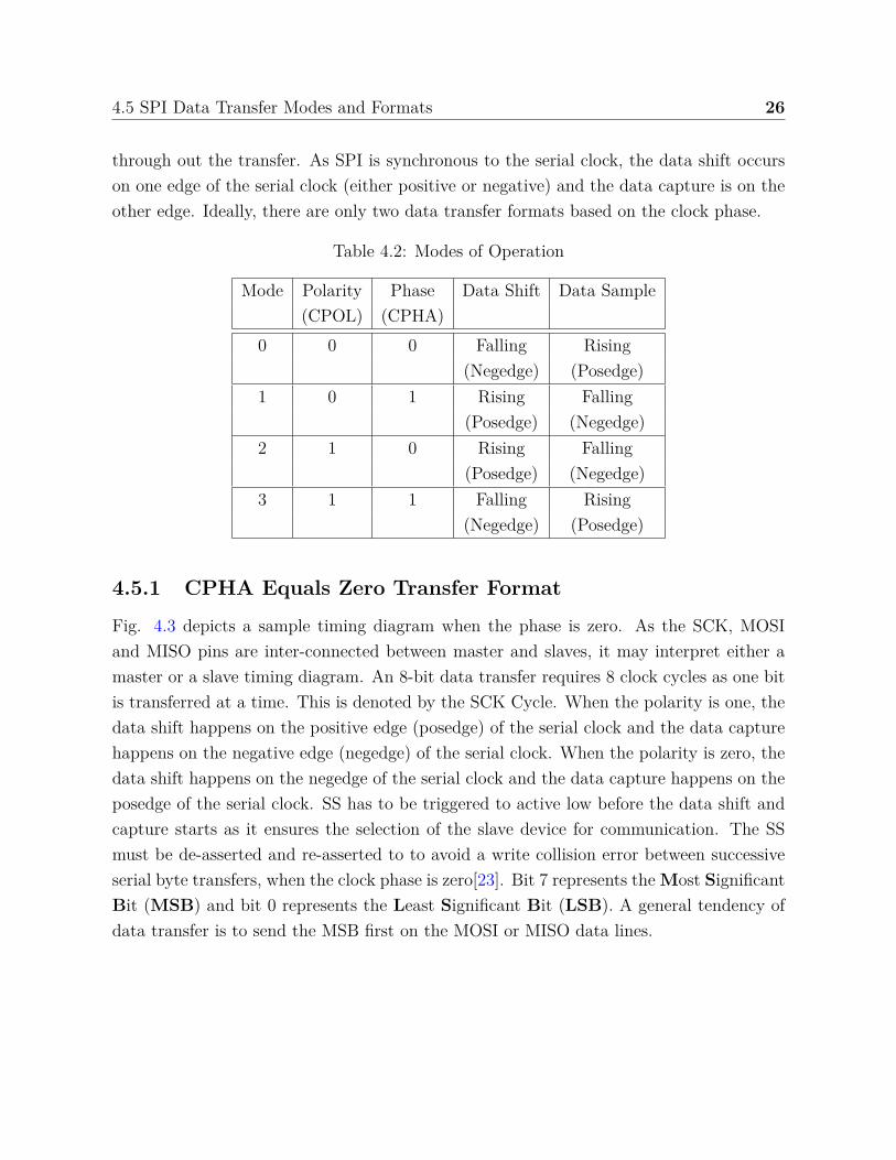
4.5 SPI Data Transfer Modes and FormatsA two-way communication is established between the microcontroller or microprocessorand the peripheral devices. The data word or character is simultaneously shifted out fromthe master to slave and shifted in from the slave to master serially one bit a clock cycle.The data sampling and shifting are synchronized by the serial clock and only after a slaveperipheral device is selected by the microcontroller or microprocessor [23]. Two bits in theSPI control register control the clock phase and polarity. There are four combinations ofthe clock phase and polarity as shown in Tab. 4.2 define the modes of operation of thedata transfer. The phase and polarity should be identical to both the master and slave
4.5 SPI Data Transfer Modes and Formats 26
through out the transfer. As SPI is synchronous to the serial clock, the data shift occurson one edge of the serial clock (either positive or negative) and the data capture is on theother edge. Ideally, there are only two data transfer formats based on the clock phase.
Table 4.2: Modes of Operation
Mode Polarity Phase Data Shift Data Sample(CPOL) (CPHA)
0 0 0 Falling Rising(Negedge) (Posedge)
1 0 1 Rising Falling(Posedge) (Negedge)
2 1 0 Rising Falling(Posedge) (Negedge)
3 1 1 Falling Rising(Negedge) (Posedge)
4.5.1 CPHA Equals Zero Transfer Format
Fig. 4.3 depicts a sample timing diagram when the phase is zero. As the SCK, MOSIand MISO pins are inter-connected between master and slaves, it may interpret either amaster or a slave timing diagram. An 8-bit data transfer requires 8 clock cycles as one bitis transferred at a time. This is denoted by the SCK Cycle. When the polarity is one, thedata shift happens on the positive edge (posedge) of the serial clock and the data capturehappens on the negative edge (negedge) of the serial clock. When the polarity is zero, thedata shift happens on the negedge of the serial clock and the data capture happens on theposedge of the serial clock. SS has to be triggered to active low before the data shift andcapture starts as it ensures the selection of the slave device for communication. The SSmust be de-asserted and re-asserted to to avoid a write collision error between successiveserial byte transfers, when the clock phase is zero[23]. Bit 7 represents the Most SignificantBit (MSB) and bit 0 represents the Least Significant Bit (LSB). A general tendency ofdata transfer is to send the MSB first on the MOSI or MISO data lines.
4.5 SPI Data Transfer Modes and Formats 27
Figure 4.3: CPHA = 0 Timing Diagram
4.5.2 CPHA Equals One Transfer Format
Fig. 4.4 depicts a sample timing diagram when the clock phase is set to one. As the SCK,MOSI and MISO pins are inter-connected between the master and slaves, it may interpreteither a master or a slave timing diagram. An 8-bit data transfer requires 8 clock cyclesas one bit is transferred at a time. This is denoted by the SCK Cycle. When the polarityis one, the data shift happens on the negedge of the serial clock and data capture happenson the posedge of the serial clock. When the polarity is zero, the data shift happens onthe posedge of the serial clock and the data capture happens on the negedge of the serialclock. SS has to be triggered to active low before the data shift and capture starts as itensures the selection of the slave device for communication. The SS can remain in theactive low state at all times, when the clock phase is 1 [23]. Bit 7 represents the MSB andbit 0 represents the LSB. A general tendency of data transfer is to send the MSB first onthe MOSI or MISO data lines.
4.6 SPI Sub-System 28
Figure 4.4: CPHA = 1 Timing Diagram
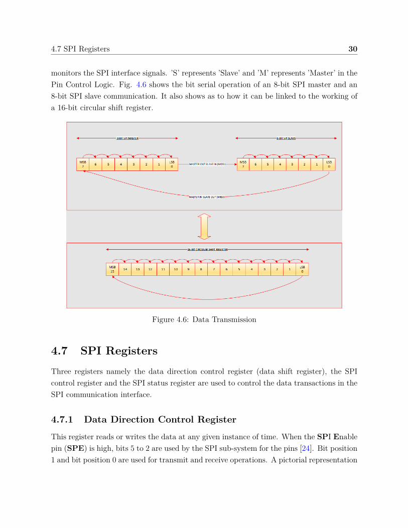
4.6 SPI Sub-SystemFig. 4.5 showcases the internal communication logic between the master and slave deviceregisters. During an 8-bit transfer in the SPI, an 8-bit character is shifted through one pinfrom the master device and another 8-bit character is shifted in through the second datapin from the slave device simultaneously. It can be understood as an 8-bit shift registerexisting in the master and the slave respectively. These two shift registers are connectedas a 16-bit shift register with a circular operation to ensure the data exchange. In Fig.4.5, a divider is used to generate the clock frequency of the SPI from the Wishbone clockas Wishbone and SPI operate at different clock frequencies. The signals and their bitpositions in the different registers are described in the Sec. 4.7.
4.6 SPI Sub-System 29
Figure 4.5: SPI Sub-System
The 8-bit shift register and the read data buffer is the central block of the Fig. 4.5. It issingle buffered in the transmit direction to ensure a new character is transferred only afterthe transfer of the previous character is complete and is double-buffered in the receivedirection [23]. The SPI status and control registers of the sub-system as shown in Fig.4.5 are used to monitor and control the status of the transaction of the character. Thetransmit and receive of data are synchronized to the serial clock. The pin control logic
4.7 SPI Registers 30
monitors the SPI interface signals. ’S’ represents ’Slave’ and ’M’ represents ’Master’ in thePin Control Logic. Fig. 4.6 shows the bit serial operation of an 8-bit SPI master and an8-bit SPI slave communication. It also shows as to how it can be linked to the working ofa 16-bit circular shift register.
Figure 4.6: Data Transmission
4.7 SPI RegistersThree registers namely the data direction control register (data shift register), the SPIcontrol register and the SPI status register are used to control the data transactions in theSPI communication interface.
4.7.1 Data Direction Control Register
This register reads or writes the data at any given instance of time. When the SPI Enablepin (SPE) is high, bits 5 to 2 are used by the SPI sub-system for the pins [24]. Bit position1 and bit position 0 are used for transmit and receive operations. A pictorial representation
4.7 SPI Registers 31
of the bits in an 8-bit SPI register is shown in the Fig. 4.7 register. The positions of thesignal representations may change as the data width increases.
Figure 4.7: Data Direction Control Register
• When SPE is high and MaSTeR (MSTR) is low, bit position 5 is the SS pinregardless of its value. When SPE and MSTR are both high, the function of SSdepends on the value in bit position 5 of the register. Value ’0’ indicates the useof SS to detect mode fault errors and value ’1’ indicates the use of SS as a generalpurpose output and this output will not be affected by the SPI sub-system [23].
• Bit position 4 of the register indicates the SCK. This bit is set high when SPI is usedas a master. This bit represents SCK regardless of its value when SPI is used as aslave [23].
• Bit position 3 of the register indicates the MOSI. It is switched to a high state ifoperated as a master and the master initiates a transaction. The value is of noimportance if operated as a slave [23].
• Bit position 2 of the register indicates the MISO. It is switched to a high state ifoperated as a slave. This value is of no importance if operated as a master [23].
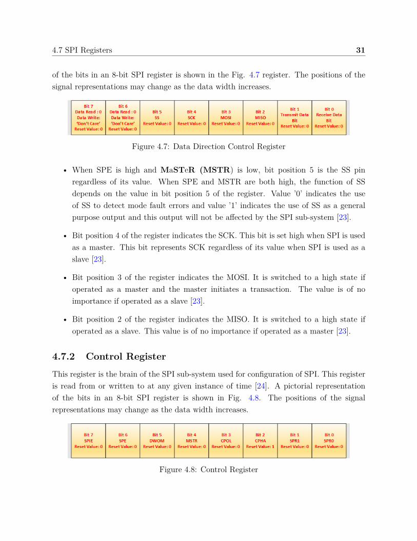
4.7.2 Control Register
This register is the brain of the SPI sub-system used for configuration of SPI. This registeris read from or written to at any given instance of time [24]. A pictorial representationof the bits in an 8-bit SPI register is shown in Fig. 4.8. The positions of the signalrepresentations may change as the data width increases.
Figure 4.8: Control Register
4.7 SPI Registers 32
• Bit position 7 indicates the enabling of SPI interrupts. It is switched to a low stateto disable the interrupts and use polling to sense the flags in the status register. Itis switched to a high state to enable the interrupts [23].
• Bit position 6 indicates the enabling of the SPI sub-system. It is enabled when sethigh.
• Bit position 5 represents the Wired OR-Mode select. This bit is set low to outputpush-pull drivers and set high to output open drain drivers [23].
• Bit position 4 is used to indicate the operation of SPI as either a master or a slavedevice. It is set high to enable SPI master operation[25][26].
• Bit position 3 is used to indicate the serial clock polarity. It is set high to enable theselection of active low clocks and vice versa[25][26].
• Bit position 2 indicates the serial clock phase to select the data transfer format[25][26].
• Bit positions 1 and 0 indicate the bit rate select bits to select the clock output fromthe divider in the SPI sub-system.
4.7.3 Status Register
This register can only be read. Write access to this register is unavailable and it containsthe status flags indicating the completion of data transfer and transfer overflow and under-run system errors. The bits in this register are set automatically based on the events ofthe SPI [24]. A pictorial representation of the bits in an 8-bit SPI register is shown in Fig.4.9. The positions of the signal representations may change as the data width increases.
Figure 4.9: Status Register
The SPI sub-system as shown in Fig. 4.5 is only concerned with the bits 7, 6 and 4.All the other bits are not used and always set low.
4.8 Beginning and Ending SPI Transfers 33
• Bit position 7 represents the flag for the completion of data transfer. It reaches ahigh state automatically at the end of the transfer. It is automatically cleaned beforea new data transfer by reading from the register with this bit in high state.
• Bit position 6 represents the flag for a write collision error. It reaches a high stateautomatically if the data direction register is written while a transfer is in progress.It is automatically cleaned before a new data transfer by reading from the registerwith this bit in high state.
• Bit position 4 indicates the mode fault error and reaches a high state the device isoperated as a master and SS goes active low. It is automatically cleaned by readingfrom this register with this bit in the high state followed by a write to the controlregister.
4.8 Beginning and Ending SPI Transfers• The clock phase data transfer format and configuration of the SPI as a master or a
slave device determines the beginning and the ending period of the transfer.
• An initiation delay occurs at the beginning and end of every SPI data transfer.
• The initiation delay is affected by the clock phase transfer format and the SPI clockrate.
• Clock phase does not affect the initiation delay but has an effect on the initial stateof the serial clock
• The SPIF bit flag in the SPI status register signifies the end of the transfer. Thisflag is set after the transfer of data based on the SPI clock rate.
4.9 Wishbone Bus InterfaceWishbone is a flexible SoC interconnection architecture used with different IP cores. Itenables a faster design re-usability by avoiding integration issues on a SoC. Wishboneinterface is used as it is independent of the various logic signaling levels of different IPcores on a chip. It employs a simple Master-Slave architecture like the SPI which makes
4.9 Wishbone Bus Interface 34
the design interface easier. Wishbone also employs parallel communication between deviceswhich results in faster execution. All the Wishbone Master and Slave devices use anINTERCONnection interface (INTERCON). INTERCON, as shown in Fig. 4.10 containsstandard logic circuits which can be used by the masters and slaves[27] [28][29].
4.9 Wishbone Bus Interface 35
Figure 4.10: Wishbone INTERCON[1]
Wishbone Master is considered as the host to the SPI. It implies that SPI master device
4.9 Wishbone Bus Interface 36
is a wishbone compliant slave device. The Wishbone signals used in interfacing with theSPI are tabulated in Tab. 4.3.
Table 4.3: Wishbone Signals[1, 5]
Signal Width Direction Descriptionwb_clk_i 1 Input System Clockwb_rst_i 1 Input Active high synchronous Resetwb_adr_i 32 Input Addresswb_dat_i 128 Input Data to Corewb_dat_o 128 Output Data from Corewb_sel_i 16 Input Byte Selectwb_we_i 1 Input Write Enablewb_stb_i 1 Input Strobewb_cyc_i 1 Input Bus cyclewb_ack_o 1 Output Bus cycle acknowledgewb_err_o 1 Output Bus cycle errorwb_int_o 1 Output Interrupt
The wishbone logic is synchronous to the system clock. Master initiates the bus trans-action. Setting the wb_rst_i to active low restarts the core, presets internal registers tothe default values and sets state machines to the initial or default known state. The hostcontroller assists the core if the interrupt wb_int_o is asserted. When asserted, a validbus cycle is checked using the signal wb_cyc_i and a valid transfer cycle is checked usingthe logical AND of the signals strobe wb_stb_i and write-enable wb_we_i. The coreresponds to the host controller only if there is a valid bus transfer cycle. A valid binarycoded address is passed to the core using the signal wb_adr_i which signifies the start ofthe bus transaction. The assertion of the signal wb_we_i signifies a Wishbone write cycleelse a Wishbone read cycle. Data is sent from the host controller to the core through thesignal wb_dat_i and the core responds to the host controller with the data through thesignal wb_dat_o. A valid bus cycle is terminated normally by asserting the acknowledgedoutput wb_ack_o. The signal wb_err_o is used to signify an error in the bus transactioncycle. [1][27][30]
Wishbone is used as it enables parallel communication in the chip. The parallel datain wishbone is converted into serial data for communication between the SPI master and
4.10 System Architecture 37
slave devices. The serial data from the slave device is converted back into parallel databefore it is sent to the Wishbone bus.
4.10 System ArchitectureFig.4.11 shows the top level system architecture. The communication interface consists ofa wishbone interface and the SPI sub-system. The SPI sub-system includes a clock dividerand a shift register. The clock divider is used as the SPI and Wishbone operate at differentclock frequencies. The shift register function is used for the data word or character exchangebetween devices. Wishbone bus communicates with the processor and the communicationis parallel. The data word from the processor is parallel and is converted into serial datafor the data exchange between devices. The serial data is converted back into parallel datato be sent to the processor.
Figure 4.11: Top-Level Architecture[2]
4.10 System Architecture 38
Fig.4.12 shows an extended architecture of the system with the interaction of the SPIregisters with the wishbone interface. As discussed in Sec. 4.7, the SPI registers includethe control register, the status register, and the data direction control register.
Figure 4.12: System Detailed Architectural Block Diagram[3]
Chapter 5
Testbench Methodology and Results
5.1 Testbench MethodologyA testbench is an additional entity that provides a repeatable set of stimuli to the designunder test to verify its functional correctness. It is portable across different simulators andchecks if the design meets the system and requirement specifications. It may be a simplehardware description file with clock and input constraints or a complex environment forerror checks, conditional checks, input constraints, and output constraints. It providesan early indication of the operation and performance of components of the design. Aflat testbench is a simple Verilog or VHDL file with clock and input constraints. A flattestbench generates inputs, resets and configures the design under test, runs tests, captureoutputs, verifies correctness and reports errors. A SystemVerilog testbench is a complexmodular environment with a higher level abstraction of the design, explicit design intent,and concise expressions. A SystemVerilog testbench focuses on the expected behavior of thesystem, as the input test combinations are automatically generated by the test generators.
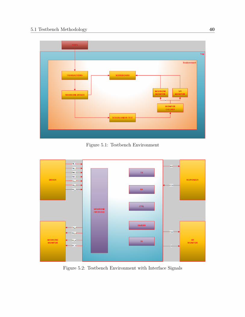
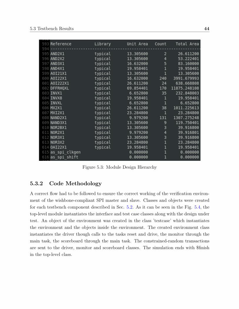
A layered testbench approach using SystemVerilog was followed in the development ofthe environment due to the benefits mentioned in Sec. 2.3 and Sec. 3.2 of this researchpaper. The developed testbench is divided into signal, command, functional and scenariolayers using object-oriented technology concepts of classes, objects, and use-cases. Thetestbench components which were developed for the verification environment using thebottom-up methodology are described in the sub-sections of this chapter. Fig. 5.1 showsthe testbench environment. Fig. 5.2 shows the testbench environment with interfacesignals.
5.1 Testbench Methodology 40
Figure 5.1: Testbench Environment
Figure 5.2: Testbench Environment with Interface Signals
5.2 Testbench Components 41
5.2 Testbench Components
5.2.1 Interface
SystemVerilog provides a useful construct named interface which helps the testbench en-vironment to interact with the design under test. The interface block will have all theWishbone and SPI signals along with modports for each protocol.
5.2.2 Transaction
The interaction between the testbench components happens through transaction objects.The transaction objects include the address of the data or transaction, the payload and thedirection of the data (either transmission or reception). The constrained-random trans-actions are passed on to the driver via transaction channels. Separate classes are createdfor the transactions to monitor and check Wishbone and SPI signals. The SPI design iscapable of transferring up to 512 bits. As it isn’t possible to determine the number ofbits to be transferred on the SPI interface, Wishbone monitor will store each 128-bit datato the SPI registers. The 512-bit data from the SPI registers along with the characterlength from the control register is sent to the scoreboard via the driver to check the SPIoutputs.The transaction objects created are randomized using the randomize function ofSystemVerilog. This is used to automate the process of generating all possible input stim-ulus and constrained-random stimulus. This approach saves time and helps in focusing onthe testbench framework and behavior of the system.The stimulus is passed to the driverthrough mailboxes.
5.2.3 Driver
A driver is used to convert the transactions into read and write operations to be sent to thecore. In this environment, it is converted into Wishbone read and write cycle operationsas Wishbone is the host controller of the system. The signals are put to a known statethrough the Wishbone reset task. The driver interacts with the design under test throughthe interface by creating it virtually.
5.2 Testbench Components 42
5.2.4 Monitor
The monitor monitors transactions at different events and also includes a checker. Itconsists of two tasks which fired in parallel as soon as the transfer of data is initiated. Onetask monitors and checks the wishbone outputs and the other task monitors and checksthe SPI interfaces. In order to make it simpler, the monitors are created as tasks in thesame class.
5.2.4.1 Wishbone Monitor
A task is created to monitor the transactions on the host-side. The purpose of a wishbonemonitor is to send the wishbone transactions to the scoreboard for analysis checks. Thestructure of the wishbone monitor is similar to that of the driver except for the transactionsto the scoreboard. This monitor is used to only check the transactions on the host side.
5.2.4.2 SPI Monitor
A task is created to monitor the transactions on the core-side. The purpose of the SPImonitor is to send the SPI transactions to the scoreboard for analysis checks. The SPImonitor generates a new transaction to be sent, waits for the transfer to be finished, makessure the transfer is complete, and ends the transmission. This is used to monitor the SPIsignals.
5.2.5 Scoreboard
The scoreboard is used to compare the actual data with the expected data. This is doneby creating a mask based on the number of bits transmitted and compare the data. Thescoreboard receives the transactions through mailboxes and the character length from theSPI control registers and it performs a compare data check. .
5.2.6 Environment
All the components developed are brought together in a unified testbench environmentcalled the environment. These components are created in the environment in the order oftheir instantiation virtually through the interface as it binds the testbench and the design.A reference is created to the SPI design as it requires specific initialization before runninga test which is done using the reset functionality.
5.3 Testbench Results 43
5.2.7 Test Case
The test case instantiates the environment and is of the file type program. A program blockinstantiates the design wrapper and the top-level class-based environment. It cannot havethe instantiation of modules, interfaces, or other programs[14]. SystemVerilog considersthis as a test module to run the different scenarios and the simulation terminates whenevery block in the program is completed. All the tasks from the respective classes are calledto enable a successful operation at the top-level of the system.
5.2.8 Top-Level
A top-level module is created to generate the clock, instantiate the interface, design undertest and the test case. It ensures the components are called the right way.
5.3 Testbench Results
5.3.1 Design’s Area, Power and Module Hierarchy
As this project is focussed on creating a functional verification environment, an open coresexisting design was updated to the latest specifications in the TSMC 0.18 micrometertechnology and only the total number of cells, total cell area and total dynamic power ofthe final design were captured in Tab. 5.1.
Table 5.1: Area and Power Details
Type ValueNumber of Cells 678
Number of Combinational cells 505Number of Sequential Cells 173
Total Cell Area 19585.84Total Dynamic Power 6.676 mWCell Internal Power 3.913 mW
Net Switching Power 2.763 mWCell Leakage Power 76.3688 mW
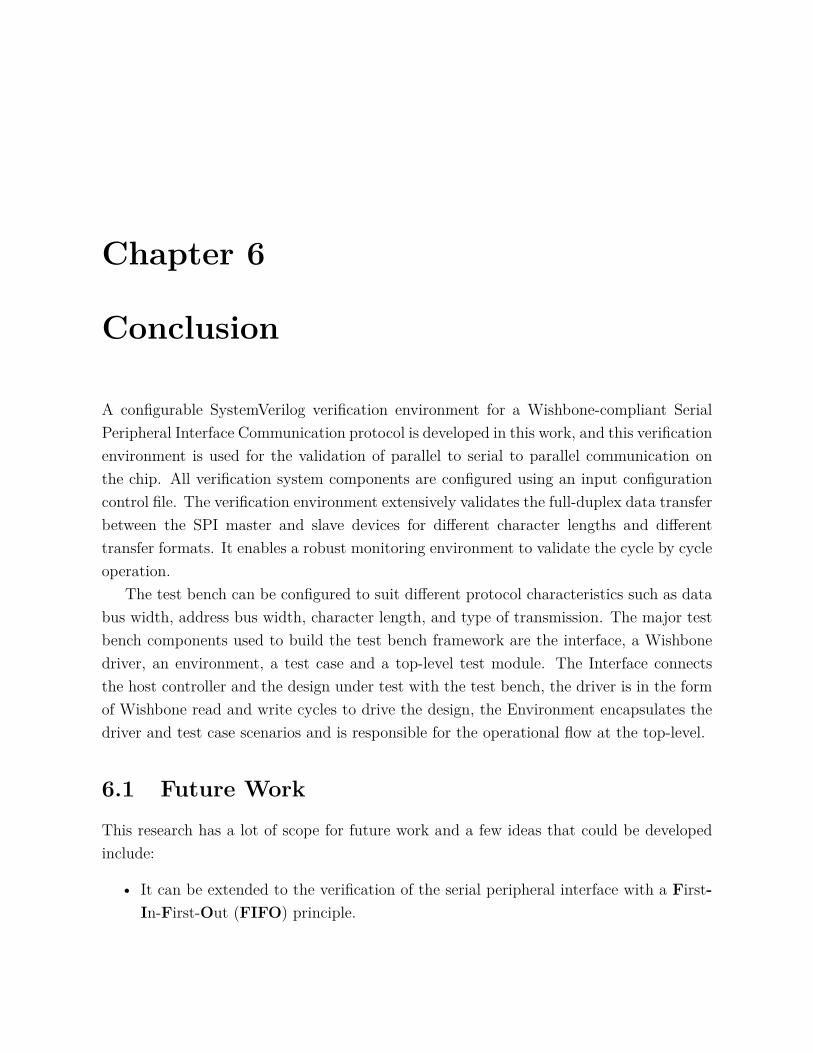
The module design hierarchy is showcased in the Fig. 5.3.
5.3 Testbench Results 44
Figure 5.3: Module Design Hierarchy
5.3.2 Code Methodology
A correct flow had to be followed to ensure the correct working of the verification environ-ment of the wishbone-compliant SPI master and slave. Classes and objects were createdfor each testbench component described in Sec. 5.2. As it can be seen in the Fig. 5.4, thetop-level module instantiates the interface and test case classes along with the design undertest. An object of the environment was created in the class ’testcase’ which instantiatesthe environment and the objects inside the environment. The created environment classinstantiates the driver though calls to the tasks reset and drive, the monitor through themain task, the scoreboard through the main task. The constrained-random transactionsare sent to the driver, monitor and scoreboard classes. The simulation ends with $finishin the top-level class.
5.3 Testbench Results 45
Figure 5.4: Code Flow
5.3.3 Wishbone and SPI Transaction Waveforms
5.3.3.1 Wishbone Transactions to SPI devices
The payload, the data and the type of the transaction is driven using the wishbone read andwrite tasks in the driver class of the environment in the Fig.5.5. This information is drivento the SPI master and slave devices through the interface signals. The communicationstarts with the assertion of the wishbone acknowledge (wb_ack_o) and it indicates thatthe slave is ready. This is visible at 240ns in the Fig. 5.5. At this time frame, The wishboneaddress (wb_adr_i) is selected as 04 and this indicates the selection of the transmit-receiveregisters. Wishbone cycle and strobe are set high, indicated by signals wb_cyc_i andwb_stb_i. Write-Enable (wb_we_i) is set low indicating a read operation from the SPI.The Wishbone Select (wb_sel_i) is always ’FFFF’ during a read or write operation as onlySPI is considered as a slave. A Wishbone address ”h 0c’ indicates selection of transmit-receive register, ”h 14’ indicates the SPI divider select value in the SPI register, ”h 18’indicates the slave select in the SPI register, and ”h 10’ indicates the SPI control in theSPI control register. When the write-enable (wb_we_i) is asserted, it indicates a writeoperation to the SPI master device. This can be seen between 420ns and 460ns in the Fig.5.5.
5.3 Testbench Results 46
Figure 5.5: Wishbone to SPI Master Transactions
5.3.3.2 SPI Master-Slave Communication
The Fig. 5.6 indicates the communication between the SPI Master initiation device andthe SPI slave peripheral device. The data received from the Wishbone is parallel data,127 bits wide and is indicated by data[127:0]. The transaction begins with an active lowslave select, indicated by ss, and remains low till the transfer of data is complete. ’sck’represents the serial clock and it synchronizes the data on mosi and miso. At 420ns, themosi is high on the rising edge of the serial clock sck. The data on this line changes onevery rising edge of the serial clock sck. It can be seen in Fig. 5.6 that data ’0101101’ isbeing sent on mosi with one-bit every clock cycle of sck during the time frame between400ns and 540ns. It can also be seen that the slave device sends all zeros during this timeframe.
Figure 5.6: SPI Master and Slave Communication
Fig. 5.7 explicitly shows the selection of the slave device through the ss_o signal andthe transfer of data from the SPI master device to slave device through the mosi_o. Thissnapshot was captured during the monitoring of the SPI signals by the monitor class ofthe environment.
5.3 Testbench Results 47
Figure 5.7: SPI Monitor Signals
Chapter 6
Conclusion
A configurable SystemVerilog verification environment for a Wishbone-compliant SerialPeripheral Interface Communication protocol is developed in this work, and this verificationenvironment is used for the validation of parallel to serial to parallel communication onthe chip. All verification system components are configured using an input configurationcontrol file. The verification environment extensively validates the full-duplex data transferbetween the SPI master and slave devices for different character lengths and differenttransfer formats. It enables a robust monitoring environment to validate the cycle by cycleoperation.
The test bench can be configured to suit different protocol characteristics such as databus width, address bus width, character length, and type of transmission. The major testbench components used to build the test bench framework are the interface, a Wishbonedriver, an environment, a test case and a top-level test module. The Interface connectsthe host controller and the design under test with the test bench, the driver is in the formof Wishbone read and write cycles to drive the design, the Environment encapsulates thedriver and test case scenarios and is responsible for the operational flow at the top-level.
6.1 Future WorkThis research has a lot of scope for future work and a few ideas that could be developedinclude:
• It can be extended to the verification of the serial peripheral interface with a First-In-First-Out (FIFO) principle.
6.1 Future Work 49
• Code coverage with respect to the standards can also be a part of the environment.
• The development of verification environment can be extended to the verification otherWishbone-compliant peripherals that support additional communication protocols.
References
[1] O. Cores, Wishbone B4 System-on-Chip (SoC)Interconnection ArchitectureforPortable IP Cores, b4 spec ed., Open Cores, 2010.
[2] R. Chen, S.-z. Huang, W. Lin, and L. Li, “Design and implementation of a reusedinterface,” in Information Science and Engineering (ICISE), 2009 1st InternationalConference on. IEEE, 2009, pp. 2603–2605.
[3] V. R. T. Deep and S. Sujatha, “Synthesis using 65nm library of spi master-slave withwishbone interface,” in International Journal of Advanced Computer Engineering andCommunication Technology, ser. 2, vol. 2, no. ISSN (Print) 2278-5140, 2013, pp. 12–16.
[4] N. Gopal, “Spi controller core: Verification,” in SSRG International Journal of VLSI& Signal Processing (SSRG-IJVSP) Volume 2 Issue 5. International Journals SSRG,2015, pp. 1–7.
[5] S. Srot, SPI Master Core Specification, rev. 0.6 ed., Open Cores, 03 2004.
[6] M. Keaveney, A. McMahon, N. O’Keeffe, K. Keane, and J. O’Reilly, “The developmentof advanced verification environments using system verilog,” IET Digital Library, 2008.
[7] C. Browy, G. Gullikson, and M. Indovina, “A top-down approach to ic design,” Inte-grated Circuit Design Methodology Guide, 1997.
[8] D. Ahlawat and N. K. Shukla, “Performance analysis of verilog directed testbenchvs constrained random systemverilog testbench,” International Journal of ComputerApplications, vol. 118, no. 22, 2015.
[9] A. Ismail and H. Saafan, “Synthesizable system verilog model for hardware metastabil-ity in formal verification,” in Electronics, Communications and Photonics Conference(SIECPC), 2013 Saudi International. IEEE, 2013, pp. 1–6.
References 51
[10] Y. Li, W. Wu, L. Hou, and H. Cheng, “A study on the assertion-based verificationof digital ic,” in Information and Computing Science, 2009. ICIC’09. Second Interna-tional Conference on, vol. 2. IEEE, 2009, pp. 25–28.
[11] Y. Tao, “An introduction to assertion-based verification,” in ASIC, 2009. ASICON’09.IEEE 8th International Conference on. IEEE, 2009, pp. 1318–1323.
[12] M.-K. You and G.-Y. Song, “Case study: Co-simulation and co-emulation environ-ments based on systemc & systemverilog,” in TENCON 2009-2009 IEEE Region 10Conference. IEEE, 2009, pp. 1–4.
[13] M.-K. You, Y.-J. Oh, and G.-Y. Song, “Implementation of a hardware functional ver-ification system using systemc infrastructure,” in TENCON 2009-2009 IEEE Region10 Conference. IEEE, 2009, pp. 1–5.
[14] C. Spear, SystemVerilog for verification: a guide to learning the testbench languagefeatures. Springer Science & Business Media, 2008.
[15] Z. Zhou, Z. Xie, X. Wang, and T. Wang, “Development of verification envioronmentfor spi master interface using systemverilog,” in Signal Processing (ICSP), 2012 IEEE11th International Conference on, vol. 3. IEEE, 2012, pp. 2188–2192.
[16] S. Cohen and L. M. Northrop, “Object-oriented technology and domain analysis,” inSoftware Reuse, 1998. Proceedings. Fifth International Conference on. IEEE, 1998,pp. 86–93.
[17] D. Ahlawat and N. K. Shukla, “Dut verification through an efficient and reusableenvironment with optimum assertion and functional coverage in systemverilog,” In-ternational Journal of Advanced Computer Science and Applications, vol. 5, no. 4,2014.
[18] D. A. S. Committee et al., “Ieee standard for systemverilog unified hardware de-sign, specification, and verification language standard ieee 1800,” http://www. edastds.org/sv/, 2012.
[19] S. Sutherland, S. Davidmann, and P. Flake, SystemVerilog for Design Second Edition:A Guide to Using SystemVerilog for Hardware Design and Modeling. Springer Science& Business Media, 2006.
References 52
[20] A. Oudjida, M. Berrandjia, A. Liacha, R. Tiar, K. Tahraoui, and Y. Alhoumays,“Design and test of general-purpose spi master/slave ips on opb bus,” in SystemsSignals and Devices (SSD), 2010 7th International Multi-Conference on. IEEE, 2010,pp. 1–6.
[21] F. Leens, “An introduction to spi and i2c protocol,” IEEE Instrumentation and Mea-surement magazine, 2009.
[22] G. HARIKA and G. R. KISHORE, “Development of reusable verification environmentfor spi protocol,” International Journal of Scientific Engineering and Technology Re-search, 2015.
[23] F. Semiconductor, M68HC11 Reference Manual, Semiconductor, Freescale, 2007.
[24] J. K. Singh, M. Tiwari, V. Sharma, and S. S. M. INDIA, “Implementation of spi–slaveon fpga,” International Journal of Advanced Engineering Technology, 2012.
[25] J. Zhang, C. Wu, W. Zhang, and J. Wang, “The design and realization of a com-prehensive spi interface controller,” in Mechanic Automation and Control Engineering(MACE), 2011 Second International Conference on. IEEE, 2011, pp. 4529–4532.
[26] M. Greco, M. P. Bussa, L. Ferrero, M. Maggiora, and A. Verna, “Vhdl implementationof a spi controller for panda digital signal processing,” in Nuclear Science Symposiumand Medical Imaging Conference (NSS/MIC), 2011 IEEE. IEEE, 2011, pp. 885–888.
[27] K. Aditya, M. Sivakumar, F. Noorbasha, and T. P. Blessington, “Design and functionalverification of a spi master slave core using system verilog,” International Journal ofSoft Computing and Engineering, vol. 2, no. 2, pp. 558–563, 2012.
[28] T. Liu and Y. Wang, “Ip design of universal multiple devices spi interface,” in Anti-Counterfeiting, Security and Identification (ASID), 2011 IEEE International Confer-ence on. IEEE, 2011, pp. 169–172.
[29] N. Anand, G. Joseph, S. S. Oommen, and R. Dhanabal, “Design and implementationof a high speed serial peripheral interface,” in Advances in Electrical Engineering(ICAEE), 2014 International Conference on. IEEE, 2014, pp. 1–3.
References 53
[30] Roopesh, Siddesha, and K. Narayan, “Rtl design and verification of spi master-slaveusing uvm,” in International Journal of Advanced Research in Electronics and Com-munication Engineering (IJARECE), August 2015 Volume 4, Issue 8, ser. 5, vol. 4,no. 2278 - 909X, IJARECE. IJARECE, 08 2015, pp. 1–4.
Appendix I
Source Code
I.1 Transactions
c l a s s t r an sa c t i on ;
// Dec la r ing the t r a n s a c t i o n srand b i t [32 −1 :0 ] addr ;rand b i t [128 −1:0 ] data ;rand trans_t kind ;
c o n s t r a i n t addr_range {addr i n s i d e {32 ’ h00000000 , 32 ’ h00000004, 32 ’ h00000008 ,
32 ’ h0000000c , 32 ’ h00000010, 32 ’ h00000014 ,
32 ’ h00000018 } ; }
endc l a s s : t r an s a c t i on
I.1 Transactions 55
c l a s s mntrsbtrans ;
// Dec la r ing the t r a n s a c t i o n srand b i t [32 −1 :0 ] addr ;rand b i t [512 −1:0 ] data ;rand trans_t kind ;rand c t r l_t c t r l ;
covergroup cg ;cove rpo int addr{
b ins v a l i d [ ] = {SPI_TXRX_0, SPI_TXRX_1, SPI_TXRX_2,SPI_TXRX_3,
SPI_CTRL, SPI_DIVIDER, SPI_SS } ;i l l e g a l _ b i n s i n v a l i d = d e f a u l t ;
}char_len : cove rpo int c t r l . char_len{
b ins t iny = { [ 1 : 1 7 1 ] } ;b ins mid = { [ 1 7 2 : 3 4 1 ] } ;b ins b ig = { 0 , [ 3 4 2 : 5 1 1 ] } ;
}coverpo int kind ;
endgroup
func t i on new ( ) ;cg = new ( ) ;
endfunct ion
func t i on sample_coverage ( ) ;
I.1 Transactions 56
cg . sample ( ) ;endfunct ion
endc l a s s : mntrsbtrans
I.2 Interface 57
I.2 Interface
i n t e r f a c e dut_int f ( input wb_clk_i ) ;
// Wishbone s i g n a l s// l o g i c wb_clk_i ;l o g i c wb_rst_i ;l o g i c [ 6 : 0 ] wb_adr_i ;l o g i c [ 1 2 7 : 0 ] wb_dat_i ;l o g i c [ 1 2 7 : 0 ] wb_dat_o ;l o g i c [ 1 5 : 0 ] wb_sel_i ;l o g i c wb_we_i ;l o g i c wb_stb_i ;l o g i c wb_cyc_i ;l o g i c wb_ack_o ;l o g i c wb_err_o ;l o g i c wb_int_o ;l o g i c test_mode ;l o g i c scan_in0 ;l o g i c scan_en ;l o g i c scan_out0 ;
// SPI s i g n a l sl o g i c [ ‘SPI_SS_NB−1:0] ss_o ;l o g i c sclk_o ;l o g i c mosi_o ;l o g i c miso_i ;
// Wishbone S i gna l s Modports to be used by the tes tbenchmodport wb ( output wb_adr_i , wb_dat_i , wb_sel_i , wb_we_i ,
I.2 Interface 58
wb_stb_i ,wb_cyc_i ,
input wb_dat_o , wb_ack_o ,wb_err_o , wb_int_o) ;
// SPI S i gna l s Modports to be used by the tes tbenchmodport sp i ( output miso_i , input ss_o , sclk_o , mosi_o ) ;
e n d i n t e r f a c e : dut_int f
I.3 Driver 59
I.3 Driver
c l a s s d r i v e r ;v i r t u a l dut_int f dut_if ;mailbox drvr2sb ;t r an sa c t i on t rans ;// scoreboard sb ;
func t i on new( v i r t u a l dut_int f dut_if , mailbox drvr2sb ) ;t h i s . dut_if = dut_if ;t h i s . drvr2sb = drvr2sb ;// t h i s . sb = sb ;
endfunct ion
task r e s e t ;dut_if . wb_rst_i = 1 ’ b0 ;r epeat (2 ) @( posedge dut_if . wb_clk_i ) ;dut_if . wb_rst_i = 1 ’ b1 ;
$d i sp l ay ( " Reset s t a r t ed . . . " ) ;dut_if .wb . wb_adr_i <= {32{1 ’bx }} ;dut_if .wb . wb_dat_i <= {128{1 ’bx }} ;dut_if .wb . wb_sel_i <= {16{1 ’bx }} ;dut_if .wb . wb_we_i <= 1 ’ hx ;dut_if .wb . wb_stb_i <= 1 ’ bx ;dut_if .wb . wb_cyc_i <= 1 ’ b0 ;$d i sp l ay ( " Reset ended . . . " ) ;
func t i on new( mailbox mntr2sb , mailbox drvr2sb ) ;t h i s . drvr2sb = drvr2sb ;t h i s . mntr2sb = mntr2sb ;
endfunct ion
task main ;mntrsbtrans trans_rcv , trans_exp ;repeat (4 ) begin
mntr2sb . get ( trans_rcv ) ;$d i sp l ay ( " Monitor Transact ion r e c e i v ed " ) ;// $d i sp l ay ( " Monitor Address : %0d , Data : %0d\n " , t rans . addr ,
t rans . data ) ;
drvr2sb . get ( trans_exp ) ;$d i sp l ay ( " Dr iver Transact ion r e c e i v ed " ) ;// $d i sp l ay ( " Dr iver Address : %0d , Data : %0d\n " , t rans . addr ,
t rans . data ) ;// i f ( trans_rcv . compare ( trans_exp ) )
// $d i sp l ay ("%0d : Transact ion matched " , $time ) ;// e l s e
// $root . e r r o r++;
// f o r ( i n t i = 0 ; i < ( t rans . c t r l & ’ h3f ) ; i++)
I.4 Scoreboard 64
//mask [ i ] = 1 ;
// i f ( ( a c tua l . data & mask) !== ( expected . data & mask) ) ;// $d i sp l ay ( " Compare Fa i l ed " ) ;
endendtask : main
endc l a s s : scoreboard
I.5 Monitor 65
I.5 Monitor
c l a s s monitor ;v i r t u a l dut_int f dut_if ;
mailbox mntr2sb ;
func t i on new( v i r t u a l dut_int f dut_if , mailbox mntr2sb ) ;t h i s . dut_if = dut_if ;t h i s . mntr2sb = mntr2sb ;
t rans . addr = dut_if . wb_adr_i ;case ( t rans . addr )
SPI_TXRX_0: t rans . data [ 1 2 7 : 0 ] = tmp_dat ;SPI_TXRX_1: t rans . data [ 2 5 5 : 1 2 8 ] = tmp_dat ;SPI_TXRX_2: t rans . data [ 3 8 3 : 2 5 6 ] = tmp_dat ;SPI_TXRX_3: t rans . data [ 5 1 1 : 3 8 4 ] = tmp_dat ;SPI_SS : ;SPI_DIVIDER : ;SPI_CTRL: t rans . c t r l = tmp_dat ;d e f a u l t : t rans . addr = ’ h1f ; // Inv a l i d
Addressendcase
i f ( t rans . addr != ’ h1f ) begin$d i sp l ay ( " Address = %0x , Data = %0x " , t rans . addr ,
tmp_dat ) ;end e l s e
$d i sp l ay ( " Address = %0x , Data = %0x " , t rans . addr ,tmp_dat ) ;
i f ( ( t rans . kind == TX) && ( trans . addr == SPI_CTRL) && (trans . c t r l & SPI_GO) )
begint rans . sample_coverage ( ) ;mntr2sb . put ( t rans ) ;
t rans = new ( ) ;
I.5 Monitor 67
end
@( posedge dut_if . wb_clk_i ) ;end : WB_ACK
endendtask : wbmon_check
task spimon_check ;f o r e v e r begin
b i t [ 6 : 0 ] i = 0 ;
mntrsbtrans t rans = new ( ) ;
whi l e ( dut_if . ss_o )begin
f o r ( i =0; dut_if . ss_o [ 0 ] ; i++)begin
@( posedge dut_if . sclk_o ) ;t rans . data [ i ] = dut_if . s p i . mosi_o ;
endend
i f ( i ) beginmntr2sb . put ( t rans ) ;
endend
endtask : spimon_check
task main ( ) ;f o rk
wbmon_check ;spimon_check ;
join_noneendtask : main
I.5 Monitor 68
endc l a s s : monitor
I.6 Environment 69
I.6 Environment
c l a s s environment ;
d r i v e r dr iv ;monitor mon ;scoreboard sb ;
mailbox mntr2sb , drvr2sb ;
v i r t u a l dut_int f i n t f ;
f unc t i on new ( v i r t u a l dut_int f i n t f ) ;t h i s . i n t f = i n t f ;t h i s . drvr2sb = drvr2sb ;t h i s . mntr2sb = mntr2sb ;d r iv = new( i n t f , drvr2sb ) ;mon = new( i n t f , mntr2sb ) ;sb = new( mntr2sb , drvr2sb ) ;
endfunct ion
endc l a s s : environment
I.7 Testcase 70
I.7 Testcase
program t e s t c a s e ( dut_int f i n t f ) ;
environment env = new( i n t f ) ;
i n i t i a lbegin
$timeformat (−9 , 2 , " ns " , 16) ;env . d r iv . r e s e t ( ) ;env . d r iv . d r i v e (10) ;env .mon . main ( ) ;env . sb . main ( ) ;
end
endprogram : t e s t c a s e
I.8 Test 71
I.8 Test
module t e s t ( ) ;
l o g i c wb_clk_i = 0 ;
i n i t i a lf o r e v e r
#5 wb_clk_i = ~wb_clk_i ;
dut_int f i n t f ( wb_clk_i ) ;
as_spi top ( i n t f . wb_rst_i , wb_clk_i , i n t f . scan_in0 , i n t f .scan_en ,
i n t f . test_mode , i n t f . scan_out0 , i n t f .wb . wb_adr_i ,i n t f .wb . wb_dat_i ,
i n t f .wb . wb_dat_o , i n t f .wb . wb_sel_i , i n t f .wb . wb_we_i,
i n t f .wb . wb_stb_i , i n t f .wb . wb_cyc_i , i n t f .wb .wb_ack_o ,
i n t f .wb . wb_err_o , i n t f .wb . wb_int_o , i n t f . s p i . ss_o ,i n t f . s p i . sclk_o , i n t f . s p i . mosi_o , i n t f . s p i . miso_i ) ;
as_spi_slave SPI_SLAVE (1 ’ b0 , i n t f . s p i . ss_o [ 0 ] , i n t f . s p i . sclk_o,
i n t f . s p i . mosi_o , i n t f . s p i . miso_i ) ;
t e s t c a s e t1 ( i n t f ) ;
endmodule : t e s t
I.9 Design Under Test 72
I.9 Design Under Test
I.9.1 Clock Generator
‘ i n c l u d e " s r c / as_sp i_def ines . v "‘ i n c l u d e " s r c / t ime s ca l e . v "
module as_spi_clkgen(
input r s t ,//System r e s e t
input in_clk ,//System Clock
input in_clk_en ,// Clock
Enableinput go ,
//Sta r t t r a n s f e r
input las t_c lk ,// Last Clock
input [ ‘SPI_DIVIDER_LEN−1:0] c lk_div ider , // Clockd i v i d e r
output reg out_clk ,//Output Clock
output reg out_clk_pos_edge ,//Output Clock p o s i t i v e edge pu l s e
output reg out_clk_neg_edge//Output Clock negat ive edge pu l s e
) ;
I.9 Design Under Test 73
reg [ ‘SPI_DIVIDER_LEN−1:0] cnt ;// Clock Counter
wirecnt_zero ;
wirecnt_one ;
a s s i gn cnt_zero = cnt == {‘SPI_DIVIDER_LEN{1 ’ b0}} ;
a s s i gn cnt_one = cnt == {{‘SPI_DIVIDER_LEN−1{1 ’b0}} , 1 ’ b1 } ;
// Clock counter count ing h a l f per iodalways @( posedge in_clk or posedge r s t ) begin
i f ( r s t )cnt <= #1 {‘SPI_DIVIDER_LEN{1 ’ b1 }} ;
‘ i n c l u d e " s r c / as_sp i_def ines . v "‘ i n c l u d e " s r c / t ime s ca l e . v "// ‘ i n c l u d e " s r c / as_spi_clkgen . v "// ‘ i n c l u d e " s r c / as_sp i_sh i f t . v "
module as_spi(
input wb_rst_i ,// Synchronous a c t i v e high
input wb_clk_i ,// Master c l o ck input
// Test Scan mode Inputs and Outputsinput scan_in0 ,
// t e s t scan mode data inputinput scan_en ,
// t e s t scan mode enableinput test_mode ,
// t e s t mode s e l e c toutput scan_out0 ,
// t e s t scan mode data output
//Wishbone Slave port s i g n a l sinput [ 6 : 0 ] wb_adr_i ,
//Lower address b i t sinput [128 −1:0 ] wb_dat_i ,
//Wishbone data outputalways @( posedge wb_clk_i or posedge wb_rst_i ) begin
i f ( wb_rst_i )wb_dat_o <= #1 128 ’ b0 ;
e l s ewb_dat_o <= #1 wb_dat ;
end
//Wishbone acknowledgealways @( posedge wb_clk_i or posedge wb_rst_i ) begin
i f ( wb_rst_i )wb_ack_o <= #1 1 ’ b0 ;
e l s ewb_ack_o <= #1 wb_cyc_i & wb_stb_i & ~wb_ack_o ;
end
//Wishbone terminat ion Errora s s i gn wb_err_o = 1 ’ b0 ;
//Wishbone In t e r rup t Requestalways @( posedge wb_clk_i or posedge wb_rst_i ) begin
i f ( wb_rst_i )wb_int_o <= #1 1 ’ b0 ;
e l s e i f ( i e && t i p && la s t_b i t && pos_edge )
I.9 Design Under Test 98
wb_int_o <= #1 1 ’ b1 ;e l s e i f (wb_ack_o)
wb_int_o <= #1 1 ’ b0 ;end
// Div ider Reg i s t e ralways @( posedge wb_clk_i or posedge wb_rst_i ) begin
i f ( wb_rst_i )d i v i d e r <= #1 {‘SPI_DIVIDER_LEN{1 ’ b0 }} ;
e l s e i f ( sp i_d iv ide r_se l && wb_we_i && ! t i p ) begin‘ i f d e f SPI_DIVIDER_LEN_8
i f ( wb_sel_i [ 0 ] )d i v i d e r <= #1 wb_dat_i [ ‘SPI_DIVIDER_LEN−1 : 0 ] ;
‘ e n d i f‘ i f d e f SPI_DIVIDER_LEN_16
i f ( wb_sel_i [ 0 ] )d i v i d e r [ 7 : 0 ] <= #1 wb_dat_i [ 7 : 0 ] ;
i f ( wb_sel_i [ 1 ] )d i v i d e r [ ‘SPI_DIVIDER_LEN−1:8] <= #1 wb_dat_i [
‘SPI_DIVIDER_LEN−1 : 8 ] ;‘ e n d i f‘ i f d e f SPI_DIVIDER_LEN_24
i f ( wb_sel_i [ 0 ] )d i v i d e r [ 7 : 0 ] <= #1 wb_dat_i [ 7 : 0 ] ;
i f ( wb_sel_i [ 1 ] )d i v i d e r [ 1 5 : 8 ] <= #1 wb_dat_i [ 1 5 : 8 ] ;
i f ( wb_sel_i [ 2 ] )d i v i d e r [ ‘SPI_DIVIDER_LEN−1:16] <= #1 wb_dat_i [
‘SPI_DIVIDER_LEN−1 : 16 ] ;‘ e n d i f‘ i f d e f SPI_DIVIDER_LEN_32
i f ( wb_sel_i [ 0 ] )d i v i d e r [ 7 : 0 ] <= #1 wb_dat_i [ 7 : 0 ] ;
i f ( wb_sel_i [ 1 ] )
I.9 Design Under Test 99
d i v i d e r [ 1 5 : 8 ] <= #1 wb_dat_i [ 1 5 : 8 ] ;i f ( wb_sel_i [ 2 ] )
d i v i d e r [ 2 3 : 1 6 ] <= #1 wb_dat_i [ 2 3 : 1 6 ] ;i f ( wb_sel_i [ 3 ] )
d i v i d e r [ ‘SPI_DIVIDER_LEN−1:24] <= #1 wb_dat_i [‘SPI_DIVIDER_LEN−1 : 24 ] ;
‘ e n d i fend
end
// Control and Status Reg i s t e ralways @( posedge wb_clk_i or posedge wb_rst_i ) begin
i f ( wb_rst_i )c t r l <= #1 {‘SPI_CTRL_BIT_NB{1 ’ b0 }} ;
e l s e i f ( s p i_c t r l_ s e l && wb_we_i && ! t i p ) begini f ( wb_sel_i [ 0 ] )
c t r l [ 7 : 0 ] <= #1 wb_dat_i [ 7 : 0 ] | {7 ’b0 , c t r l [ 0 ] } ;i f ( wb_sel_i [ 1 ] )
c t r l [ ‘SPI_CTRL_BIT_NB−1:8] <= #1 wb_dat_i [ ‘SPI_CTRL_BIT_NB−1 : 8 ] ;
ende l s e i f ( t i p && la s t_b i t && pos_edge )
c t r l [ ‘SPI_CTRL_GO] <= #1 1 ’ b0 ;end
a s s i gn rx_negedge = c t r l [‘SPI_CTRL_RX_NEGEDGE] ;a s s i gn tx_negedge = c t r l [‘SPI_CTRL_TX_NEGEDGE] ;a s s i gn go = c t r l [ ‘SPI_CTRL_GO ] ;a s s i gn char_len = c t r l [ ‘SPI_CTRL_CHAR_LEN ] ;a s s i gn l s b = c t r l [ ‘SPI_CTRL_LSB ] ;a s s i gn i e = c t r l [ ‘SPI_CTRL_IE ] ;a s s i gn as s = c t r l [ ‘SPI_CTRL_ASS ] ;
I.9 Design Under Test 100
// Slave S e l e c t Reg i s t e ralways @( posedge wb_clk_i or posedge wb_rst_i ) begin
i f ( wb_rst_i )s s <= #1 {‘SPI_SS_NB{1 ’ b0 }} ;
e l s e i f ( sp i_ss_se l && wb_we_i && ! t i p ) begin‘ i f d e f SPI_SS_NB_8
i f ( wb_sel_i [ 0 ] )s s <= #1 wb_dat_i [ ‘SPI_SS_NB −1 : 0 ] ;
‘ e n d i f‘ i f d e f SPI_SS_NB_16
i f ( wb_sel_i [ 0 ] )s s [ 7 : 0 ] <= #1 wb_dat_i [ 7 : 0 ] ;
i f ( wb_sel_i [ 1 ] )s s [ ‘SPI_SS_NB−1:8] <= #1 wb_dat_i [ ‘SPI_SS_NB −1 : 8 ] ;
‘ e n d i f‘ i f d e f SPI_SS_24
i f ( wb_sel_i [ 0 ] )s s [ 7 : 0 ] <= #1 wb_dat_i [ 7 : 0 ] ;
i f ( wb_sel_i [ 1 ] )s s [ 1 5 : 8 ] <= #1 wb_dat_i [ 1 5 : 8 ] ;
i f ( wb_sel_i [ 2 ] )s s [ ‘SPI_SS_NB−1:16] <= #1 wb_dat_i [ ‘SPI_SS_NB −1 : 16 ] ;
‘ e n d i f‘ i f d e f SPI_SS_NB_32
i f ( wb_sel_i [ 0 ] )s s [ 7 : 0 ] <= #1 wb_dat_i [ 7 : 0 ] ;
i f ( wb_sel_i [ 1 ] )s s [ 1 5 : 8 ] <= #1 wb_dat_i [ 1 5 : 8 ] ;
i f ( wb_sel_i [ 2 ] )s s [ 2 3 : 1 6 ] <= #1 wb_dat_i [ 2 3 : 1 6 ] ;
i f ( wb_sel_i [ 3 ] )s s [ ‘SPI_SS_NB−1:24] <= #1 wb_dat_i [ ‘SPI_SS_NB −1 : 24 ] ;
‘ e n d i f
I.9 Design Under Test 101
endend
a s s i gn ss_o = ~(( s s & {‘SPI_SS_NB{ t i p & ass }}) | ( s s & {‘SPI_SS_NB{ ! as s }}) ) ;
as_spi_clkgen Clock_Gen (. r s t ( wb_rst_i ) ,. in_clk ( wb_clk_i ) ,
. in_clk_en ( t i p ) ,
. go ( go ) ,
. l a s t_c lk ( l a s t_b i t ) ,
. c l k_d iv ide r ( d i v i d e r ) ,
. out_clk ( sclk_o ) ,
. out_clk_pos_edge ( pos_edge ) ,
. out_clk_neg_edge ( neg_edge )) ;
a s_sp i_sh i f t SHIFT_REGISTER(
. r s t ( wb_rst_i ) ,
. c l k ( wb_clk_i ) ,. l a t ch ( spi_tx_se l [ 3 : 0 ] & {4{wb_we_i}}) ,. byte_se l ( wb_sel_i ) ,. l en ( char_len [ ‘SPI_CHAR_LEN_BITS−1 :0 ] ) ,. l s b ( l s b ) ,. go ( go ) ,. pos_edge ( pos_edge ) ,. neg_edge ( neg_edge ) ,. rx_negedge ( rx_negedge ) ,. tx_negedge ( tx_negedge ) ,. t i p ( t i p ) ,
. l a s t ( l a s t_b i t ) ,. p_in (wb_dat_i ) ,
I.9 Design Under Test 102
. p_out ( rx ) ,
. s_clk ( sclk_o ) ,
. s_in ( miso_i ) ,
. s_out ( mosi_o )) ;
endmodule // as_spi
I.9 Design Under Test 103
I.9.4 SPI Slave
‘ i n c l u d e " s r c / t ime s ca l e . v "
module as_spi_slave(input r s t ,
// Resetinput ss ,
// Slave S e l e c tinput sc lk ,
// S e r i a l Clockinput mosi ,
// Master Out Slave Inoutput reg miso // Master
In Slave Out) ;
reg rx_negedge ; //DataReceived on negedge
reg tx_negedge ;//Data transmit ted on negedge
reg [ 1 2 7 : 0 ] data ;//Data r e g i s t e r
always @( posedge ( s c l k && ! rx_negedge ) or negedge ( s c l k &&rx_negedge ) or r s t ) begin
i f ( r s t )data <= #1 128 ’ b0 ;
e l s e i f ( ! s s )data <= #1 {data [ 1 2 6 : 0 ] , mosi } ;
I.9 Design Under Test 104
end
always @( posedge ( s c l k && ! tx_negedge ) or negedge ( s c l k &&tx_negedge ) ) begin