16

T-411-MECH
Lab Report 3
Arduino Dimmer Unit
Instructor: Joseph Timothy Foley
Axel Bender & Arndís Magnúsdóttir
November 16, 2012

Contents
Contents 1
1 Introduction 2
2 Materials and Methods 32.1 Materials . . . . . . . . . . . . . . . . . . . . . . . . . . . . . . . . . . . . . . . 32.2 Procedure . . . . . . . . . . . . . . . . . . . . . . . . . . . . . . . . . . . . . . . 4
2.2.1 Diode rectication . . . . . . . . . . . . . . . . . . . . . . . . . . . . . . 42.3 BJT amplication . . . . . . . . . . . . . . . . . . . . . . . . . . . . . . . . . . . 52.4 MOSFET binary switch . . . . . . . . . . . . . . . . . . . . . . . . . . . . . . . 5
3 Results and Discussions 73.1 Half-bridge and full-bridge rectiers . . . . . . . . . . . . . . . . . . . . . . . . . 7
3.1.1 Diode circuit . . . . . . . . . . . . . . . . . . . . . . . . . . . . . . . . . 83.1.2 Diode and capacitor circuit . . . . . . . . . . . . . . . . . . . . . . . . . 83.1.3 full-bridge rectier circuit . . . . . . . . . . . . . . . . . . . . . . . . . . 9
3.2 BJT circuit . . . . . . . . . . . . . . . . . . . . . . . . . . . . . . . . . . . . . . 93.3 Transistors . . . . . . . . . . . . . . . . . . . . . . . . . . . . . . . . . . . . . . . 11
3.3.1 P-type MOSFET . . . . . . . . . . . . . . . . . . . . . . . . . . . . . . . 123.3.2 N-type MOSFET . . . . . . . . . . . . . . . . . . . . . . . . . . . . . . . 123.3.3 Arduino Dimmer . . . . . . . . . . . . . . . . . . . . . . . . . . . . . . . 12
4 Conclusions 13
5 Appendix 145.1 Calculations & equations . . . . . . . . . . . . . . . . . . . . . . . . . . . . . . . 14
5.1.1 BJT amplication . . . . . . . . . . . . . . . . . . . . . . . . . . . . . . . 145.2 Arduino code . . . . . . . . . . . . . . . . . . . . . . . . . . . . . . . . . . . . . 14
6 References 15
1
1 Introduction
This particular exercise focuses on the use of diodes and transistors to rectify an AC signaland using transistors to control large amount of current with a proportionally small current.To do this we will be utilizing semiconductor transistors, bipolar junction transistor (BJT)and metal-oxide-semiconductor eld-eect transistor (MOSFET). These are usually chosen forengineering projects for their ability to amplify a signal but will mostly be used in this exercisefor their ability to work as switches, MOSFET in particular. Diodes are used in this exercisefor their electrical property, that is they work as one way shut o valve and only allow currentto ow in one direction.
Semiconductors Are somewhat an intermediate between a conductor and an insulator.What characterizes semiconductors is their inherent property of increasing conductivity withincreasing temperature and the fact that their behavioural aspect can be modied by a processcalled doping[1].
Diodes Most common type of diodes, semiconductor diode, are made of two semiconductorcrystal types called the P-type and N-type. The letters P and N are in relation to weatherthe crystal has more positive charge carriers(P-type) or negative carriers(N-type)[1]. Thesedierent types of semiconductor crystals are created by adding impurities (i.e. doping) tothem. The two crystals are separated by a zone called the Depletion region due to the absenceof a charger carrier. When a current is sent through the diode the carriers do either help orhinder the current, depending on the direction the current is owing over the P-N junction.
BJT Consist of three dierent types of doped semiconductors, the emitter region, collectorregion and base region. These region are either P-type or N-type and depending on how theyare arranged together can form a PNP transistor and a NPN transistor. The BJT's architectureis usually that the base is located between the collector and emitter [1]. This type of transistoris very useful as a amplier because a small current owing from base to emitter (IBE) canopen a passageway for a larger current owing through the length of the transistor (ICE). Itcan also be used as a switch or in oscillators. The correlation between IBE and ICE can be seenin the following formula. 1
ICE = β · IBE (1)
MOSFET Is a four-terminal device with source, gate, drain and base terminals. But withthe base connected to the source terminal, as it is most commonly used, makes it a tree-terminaldevice much like any other eld-eect transistors. The source and drain terminals are made oftwo semiconductor crystallines, either both N-type or P-type, and are embedded in the basewhich is made of the opposite type of semiconductor crystal. The two source and drain ter-minals are connected via a thin layer of silicon dioxide which is then covered by another thinsheet of metal, which in turn makes up the terminal called gate. When a voltage is appliedbetween the gate and base terminal it creates and electric eld which penetrates through theinsulating oxide of the gate terminal, creating a channel of the same N or P-type as the sourceand drain allowing a current to pass through[1]. This makes a MOSFET a very aective deviceto be used for amplifying or switching electronic signals.
In this experiment we start by rectifying an AC signal using diodes and capacitors, this partis threefold. We start by building a circuit with a diode and a resistor to cut-o the backow ofthe 2.5 V AC input. Next up we add a capacitor, in parallel to the diode, to the circuit to fade
2

out the amplitude of the sine waveform in eort to make the AC signal resemble a DC signal.Lastly a circuit including full-bridge rectier will be constructed in attempt to rectifying thesame 2.5 V AC signal. In the second part of the experiment we will be using a BJT transistorto amplify a DC signal and assess β for the transistor by taking 10 measurements of the gainfrom the amplier. For the last part of this experiment we will start by familiarize ourselveswith some N-channel and P-channel MOSFETs through experimentation. Then we will build adimmer using an Arduino unit to control how much current ows, from a 15 V external powersupply, through a MOSFET switch and to the diode.
2 Materials and Methods
2.1 Materials
• 4 diodes, number: IN4148
• 1,08 kΩ
• 9,86 kΩ
• 330 kΩ
• Two 10 kΩ
• NI ELVIS - National Instruments, number: 7456, serial number: 12CCCEC, markedhopur 3.
• Multi-meter(DMM), MFR number: 062250740, Made in Taiwan
• 20 µF capacitor
• 1 BJT, number: BC547
• 1 P-type MOSFET: 1BFD9110
• 1 N-type MOSFET: 1BFD110
• Oscilloscope: Labview
• Computer with National Instruments software installed, number: 5865,Marked hopur 4.
• 10 LED lights.
• 2 big buttons
• Breadboard on the ELVIS, number: 5865
• Arduino microcontroller
• Small breadboard which is stuck to the Arduino microcontroller
• Lenovo laptop with Arduino 1.0.1 software installed.
3
2.2 Procedure
2.2.1 Diode rectication
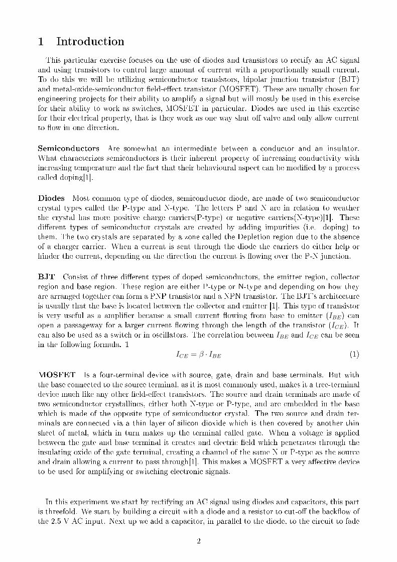
We connected a simple half-bridge rectier circuit with a diode and a 9,86 kΩ to the ELVISbreadboard, see gure 1 on how it was connected. By using a diode we lter out the bottompart of the sine wave and by doing so we are going closer to a DC output. A diode is wade out ofsilicon and acts as a valve for it has uneven charges. A half of the diode is a positively-chargedand the other half is negatively-charged. Because the diode acts as a valve the current onlyows in on direction and it's the reason for the bottom cut of the AC sine wave, see gure8. We used the oscilloscope on the ELVIS to monitor the input (channel A, green wave) andthe output (channel B, blue wave)of the circuit is the half-sine wave where the diode cuts othe bottom part. Before the sine wave was bipolar and now it only has one pole. We set thevoltage on the function generator to 2.5 V and approximately 50 Hz frequency.
Figure 1: A half-bridge rectier with a single diode, gure gotten from instruction manual [2]
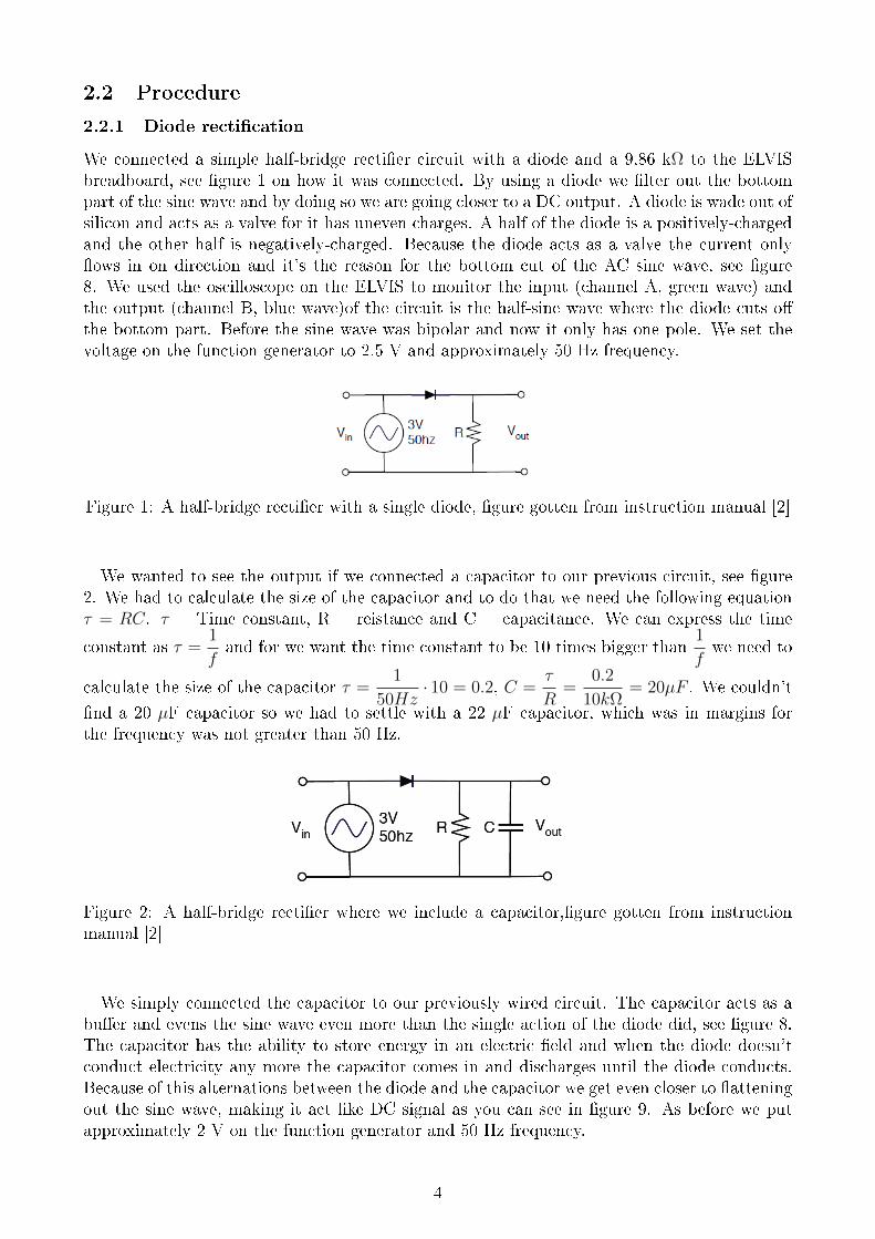
We wanted to see the output if we connected a capacitor to our previous circuit, see gure2. We had to calculate the size of the capacitor and to do that we need the following equationτ = RC. τ = Time constant, R = reistance and C = capacitance. We can express the time
constant as τ =1
fand for we want the time constant to be 10 times bigger than
1
fwe need to
calculate the size of the capacitor τ =1
50Hz· 10 = 0.2, C =
τ
R=
0.2
10kΩ= 20µF . We couldn't
nd a 20 µF capacitor so we had to settle with a 22 µF capacitor, which was in margins forthe frequency was not greater than 50 Hz.
Figure 2: A half-bridge rectier where we include a capacitor,gure gotten from instructionmanual [2]
We simply connected the capacitor to our previously wired circuit. The capacitor acts as abuer and evens the sine wave even more than the single action of the diode did, see gure 8.The capacitor has the ability to store energy in an electric eld and when the diode doesn'tconduct electricity any more the capacitor comes in and discharges until the diode conducts.Because of this alternations between the diode and the capacitor we get even closer to atteningout the sine wave, making it act like DC signal as you can see in gure 9. As before we putapproximately 2 V on the function generator and 50 Hz frequency.
4
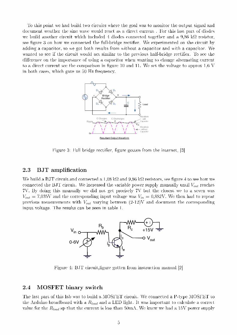
To this point we had build two circuits where the goal was to monitor the output signal anddocument weather the sine wave would react as a direct current . For this last part of diodeswe build another circuit which included 4 diodes connected together and a 9,86 kΩ resistor,see gure 3 on how we connected the full-bridge rectier. We experimented on the circuit byadding a capacitor, so we got both results from without a capacitor and with a capacitor. Wewanted to see if the circuit would act similar to the previous half-bridge rectier. To see thedierence on the importance of using a capacitor when wanting to change alternating currentto a direct current see the comparison in gure 10 and 11. We set the voltage to approx 1,6 Vin both cases, which gave us 50 Hz frequency.
Figure 3: Full bridge rectier, gure gotten from the internet, [3]
2.3 BJT amplication
We build a BJT circuit and connected a 1,08 kΩ and 9,86 kΩ resistors, see gure 4 to see how weconnected the BJT circuit. We increased the variable power supply manually until Vout reaches7V. By doing this manually we did not get precisely 7V but the closest we to a seven wasVout = 7,035V and the corresponding input voltage was Vin = 0,882V. We then had to repeatprevious measurements with Vout varying between (2-12)V and document the correspondinginput voltage. The results can be seen in table 1.
Figure 4: BJT circuit,gure gotten from instruction manual [2]
2.4 MOSFET binary switch
The last part of this lab was to build a MOSFET circuit. We connected a P-type MOSFET tothe Arduino breadboard with a Rload and a LED light. It was important to calculate a correctvalue for the Rload sp that the current is less than 50mA. We knew we had a 15V power supply
5
so the correct value for the resistance is calculated Rload =15V
50mA= 300Ω. We could not nd a
300Ω resistor and we need the current to be less than 50mA so we used instead a 330Ω resistor.
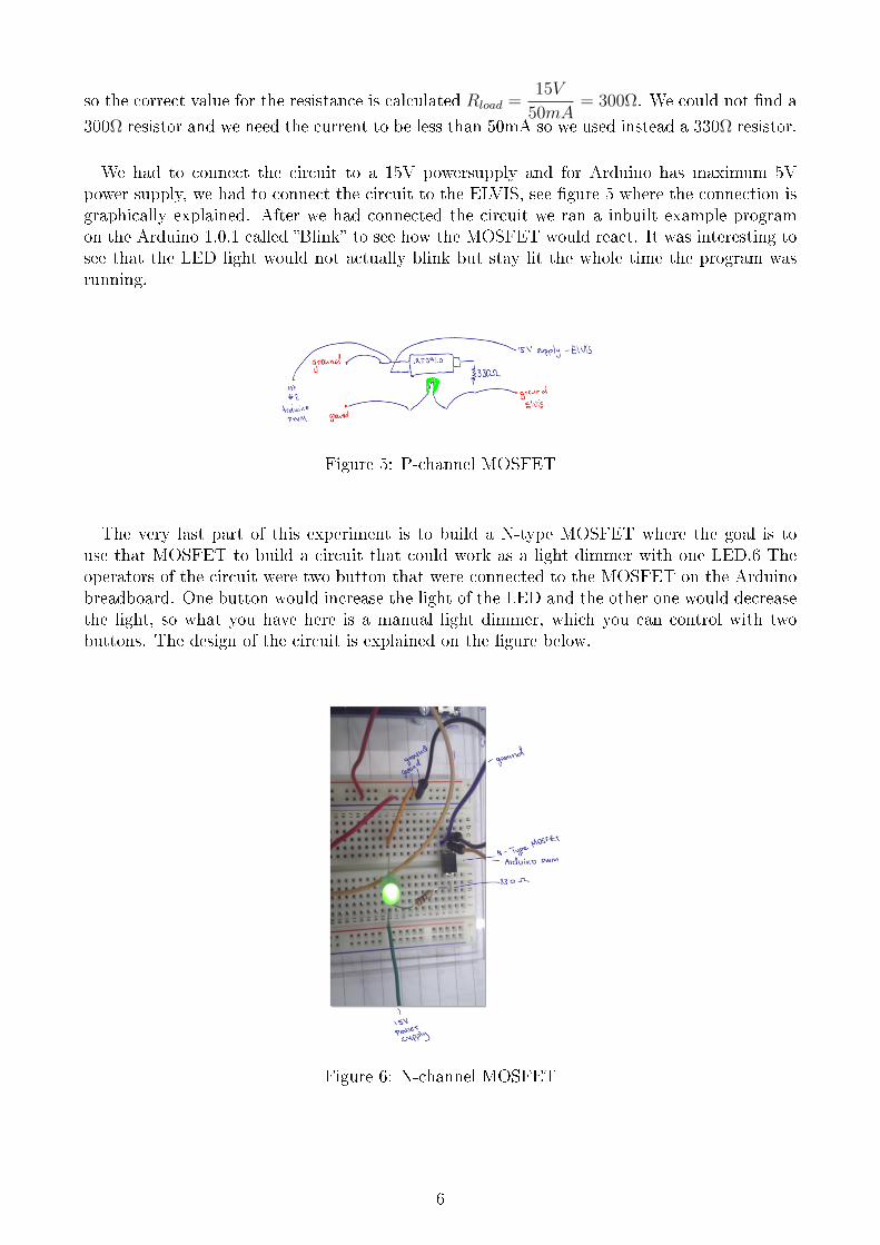
We had to connect the circuit to a 15V powersupply and for Arduino has maximum 5Vpower supply, we had to connect the circuit to the ELVIS, see gure 5 where the connection isgraphically explained. After we had connected the circuit we ran a inbuilt example programon the Arduino 1.0.1 called Blink to see how the MOSFET would react. It was interesting tosee that the LED light would not actually blink but stay lit the whole time the program wasrunning.
Figure 5: P-channel MOSFET
The very last part of this experiment is to build a N-type MOSFET where the goal is touse that MOSFET to build a circuit that could work as a light dimmer with one LED.6 Theoperators of the circuit were two button that were connected to the MOSFET on the Arduinobreadboard. One button would increase the light of the LED and the other one would decreasethe light, so what you have here is a manual light dimmer, which you can control with twobuttons. The design of the circuit is explained on the gure below.
Figure 6: N-channel MOSFET
6
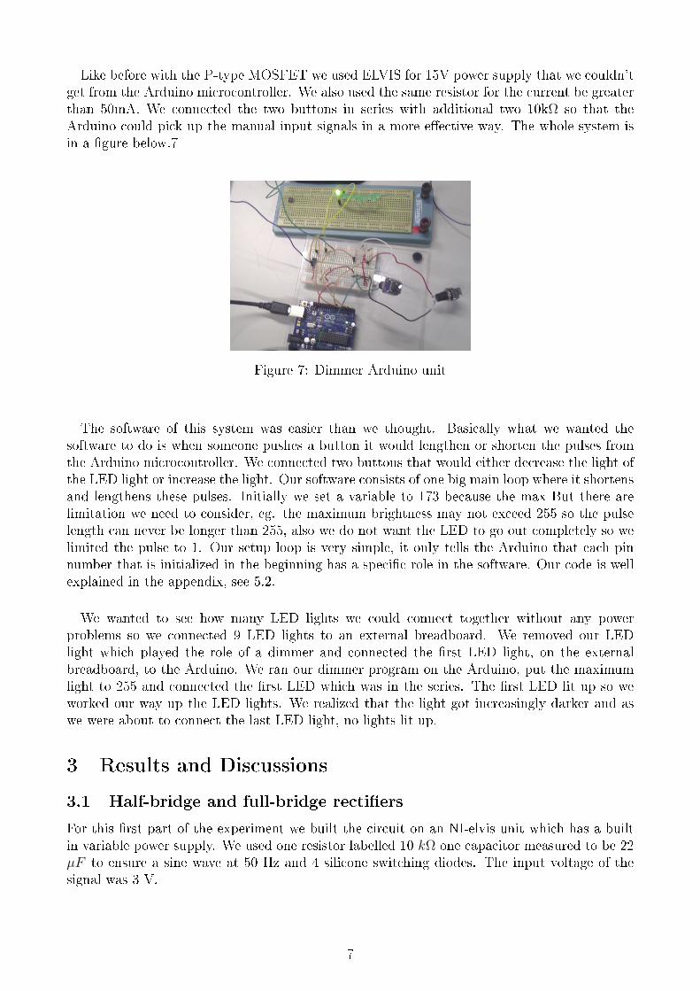
Like before with the P-type MOSFET we used ELVIS for 15V power supply that we couldn'tget from the Arduino microcontroller. We also used the same resistor for the current be greaterthan 50mA. We connected the two buttons in series with additional two 10kΩ so that theArduino could pick up the manual input signals in a more eective way. The whole system isin a gure below.7
Figure 7: Dimmer Arduino unit
The software of this system was easier than we thought. Basically what we wanted thesoftware to do is when someone pushes a button it would lengthen or shorten the pulses fromthe Arduino microcontroller. We connected two buttons that would either decrease the light ofthe LED light or increase the light. Our software consists of one big main loop where it shortensand lengthens these pulses. Initially we set a variable to 173 because the max But there arelimitation we need to consider, eg. the maximum brightness may not exceed 255 so the pulselength can never be longer than 255, also we do not want the LED to go out completely so welimited the pulse to 1. Our setup loop is very simple, it only tells the Arduino that each pinnumber that is initialized in the beginning has a specic role in the software. Our code is wellexplained in the appendix, see 5.2.
We wanted to see how many LED lights we could connect together without any powerproblems so we connected 9 LED lights to an external breadboard. We removed our LEDlight which played the role of a dimmer and connected the rst LED light, on the externalbreadboard, to the Arduino. We ran our dimmer program on the Arduino, put the maximumlight to 255 and connected the rst LED which was in the series. The rst LED lit up so weworked our way up the LED lights. We realized that the light got increasingly darker and aswe were about to connect the last LED light, no lights lit up.
3 Results and Discussions
3.1 Half-bridge and full-bridge rectiers
For this rst part of the experiment we built the circuit on an NI-elvis unit which has a builtin variable power supply. We used one resistor labelled 10 kΩ one capacitor measured to be 22µF to ensure a sine wave at 50 Hz and 4 silicone switching diodes. The input voltage of thesignal was 3 V.
7
3.1.1 Diode circuit
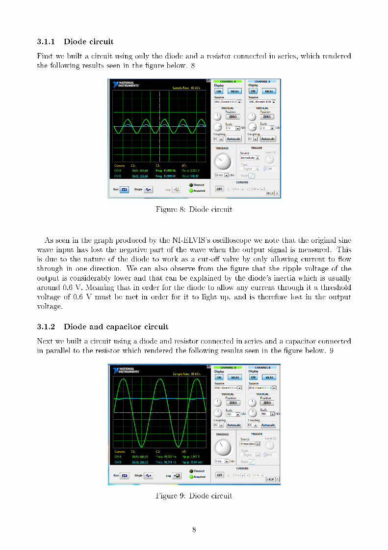
First we built a circuit using only the diode and a resistor connected in series, which renderedthe following results seen in the gure below. 8
Figure 8: Diode circuit
As seen in the graph produced by the NI-ELVIS's oscilloscope we note that the original sinewave input has lost the negative part of the wave when the output signal is measured. Thisis due to the nature of the diode to work as a cut-o valve by only allowing current to owthrough in one direction. We can also observe from the gure that the ripple voltage of theoutput is considerably lower and that can be explained by the diode's inertia which is usuallyaround 0.6 V. Meaning that in order for the diode to allow any current through it a thresholdvoltage of 0.6 V must be met in order for it to light up, and is therefore lost in the outputvoltage.
3.1.2 Diode and capacitor circuit
Next we built a circuit using a diode and resistor connected in series and a capacitor connectedin parallel to the resistor which rendered the following results seen in the gure below. 9
Figure 9: Diode circuit
8
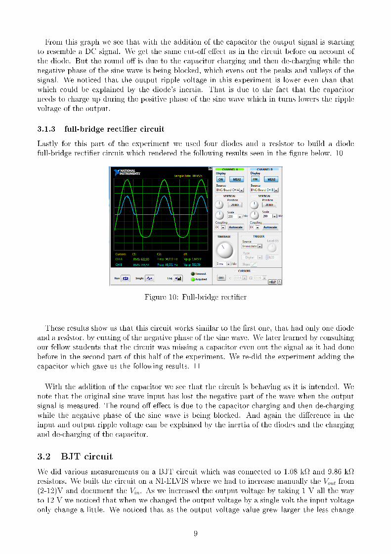
From this graph we see that with the addition of the capacitor the output signal is startingto resemble a DC signal. We get the same cut-o eect as in the circuit before on account ofthe diode. But the round o is due to the capacitor charging and then de-charging while thenegative phase of the sine wave is being blocked, which evens out the peaks and valleys of thesignal. We noticed that the output ripple voltage in this experiment is lower even than thatwhich could be explained by the diode's inertia. That is due to the fact that the capacitorneeds to charge up during the positive phase of the sine wave which in turns lowers the ripplevoltage of the output.
3.1.3 full-bridge rectier circuit
Lastly for this part of the experiment we used four diodes and a resistor to build a diodefull-bridge rectier circuit which rendered the following results seen in the gure below. 10
Figure 10: Full-bridge rectier
These results show us that this circuit works similar to the rst one, that had only one diodeand a resistor, by cutting of the negative phase of the sine wave. We later learned by consultingour fellow students that the circuit was missing a capacitor even out the signal as it had donebefore in the second part of this half of the experiment. We re-did the experiment adding thecapacitor which gave us the following results. 11
With the addition of the capacitor we see that the circuit is behaving as it is intended. Wenote that the original sine wave input has lost the negative part of the wave when the outputsignal is measured. The round o eect is due to the capacitor charging and then de-chargingwhile the negative phase of the sine wave is being blocked. And again the dierence in theinput and output ripple voltage can be explained by the inertia of the diodes and the chargingand de-charging of the capacitor.
3.2 BJT circuit
We did various measurements on a BJT circuit which was connected to 1.08 kΩ and 9.86 kΩresistors. We built the circuit on a NI-ELVIS where we had to increase manually the Vout from(2-12)V and document the Vin. As we increased the output voltage by taking 1 V all the wayto 12 V we noticed that when we changed the output voltage by a single volt the input voltageonly change a little. We noticed that as the output voltage value grew larger the less change
9
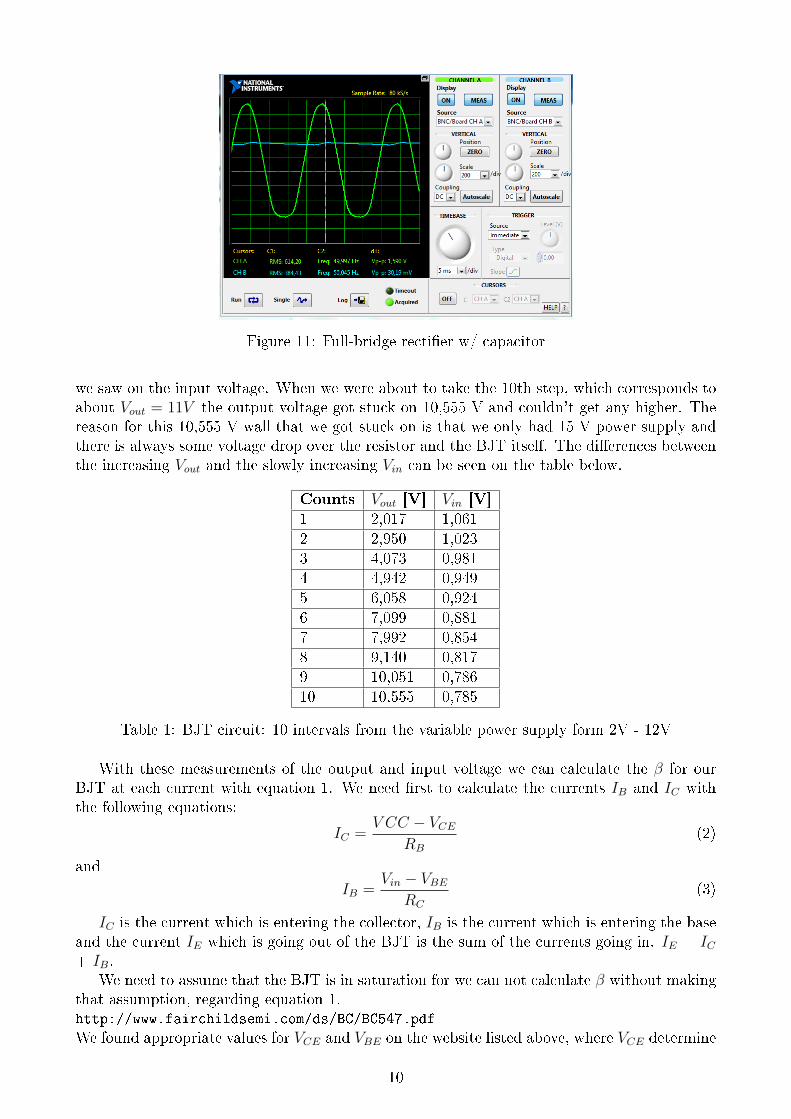
Figure 11: Full-bridge rectier w/ capacitor
we saw on the input voltage. When we were about to take the 10th step, which corresponds toabout Vout = 11V the output voltage got stuck on 10,555 V and couldn't get any higher. Thereason for this 10,555 V wall that we got stuck on is that we only had 15 V power supply andthere is always some voltage drop over the resistor and the BJT itself. The dierences betweenthe increasing Vout and the slowly increasing Vin can be seen on the table below.
Counts Vout [V] Vin [V]1 2,017 1,0612 2,950 1,0233 4,073 0,9814 4,942 0,9495 6,058 0,9246 7,099 0,8817 7,992 0,8548 9,140 0,8179 10,051 0,78610 10,555 0,785
Table 1: BJT circuit: 10 intervals from the variable power supply form 2V - 12V
With these measurements of the output and input voltage we can calculate the β for ourBJT at each current with equation 1. We need rst to calculate the currents IB and IC withthe following equations:
IC =V CC − VCE
RB
(2)
and
IB =Vin − VBE
RC
(3)
IC is the current which is entering the collector, IB is the current which is entering the baseand the current IE which is going out of the BJT is the sum of the currents going in. IE = IC+ IB.
We need to assume that the BJT is in saturation for we can not calculate β without makingthat assumption, regarding equation 1.http://www.fairchildsemi.com/ds/BC/BC547.pdf
We found appropriate values for VCE and VBE on the website listed above, where VCE determine
10
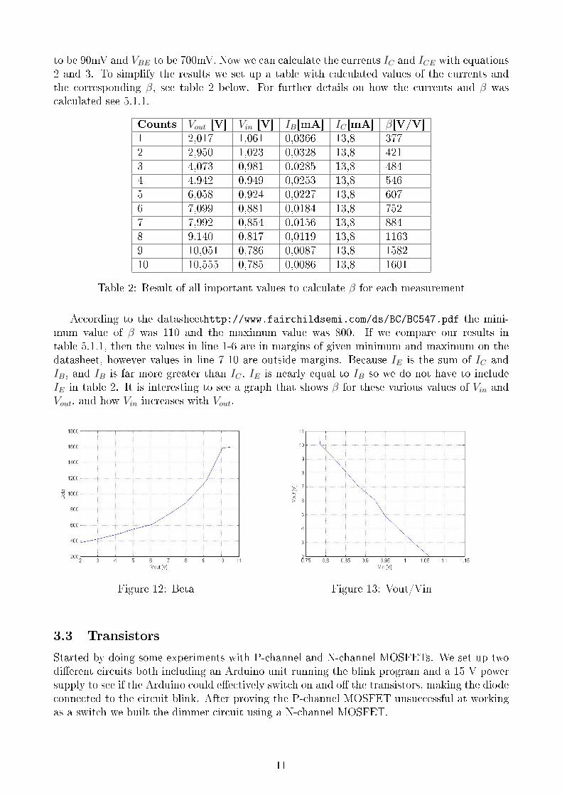
to be 90mV and VBE to be 700mV. Now we can calculate the currents IC and ICE with equations2 and 3. To simplify the results we set up a table with calculated values of the currents andthe corresponding β, see table 2 below. For further details on how the currents and β wascalculated see 5.1.1.
Counts Vout [V] Vin [V] IB[mA] IC[mA] β[V/V]1 2,017 1,061 0,0366 13,8 3772 2,950 1,023 0,0328 13,8 4213 4,073 0,981 0,0285 13,8 4844 4,942 0,949 0,0253 13,8 5465 6,058 0,924 0,0227 13,8 6076 7,099 0,881 0,0184 13,8 7527 7,992 0,854 0,0156 13,8 8848 9,140 0,817 0,0119 13,8 11639 10,051 0,786 0,0087 13,8 158210 10,555 0,785 0,0086 13,8 1601
Table 2: Result of all important values to calculate β for each measurement
According to the datasheethttp://www.fairchildsemi.com/ds/BC/BC547.pdf the mini-mum value of β was 110 and the maximum value was 800. If we compare our results intable 5.1.1, then the values in line 1-6 are in margins of given minimum and maximum on thedatasheet, however values in line 7-10 are outside margins. Because IE is the sum of IC andIB, and IB is far more greater than IC , IE is nearly equal to IB so we do not have to includeIE in table 2. It is interesting to see a graph that shows β for these various values of Vin andVout, and how Vin increases with Vout.
Figure 12: Beta Figure 13: Vout/Vin
3.3 Transistors
Started by doing some experiments with P-channel and N-channel MOSFETs. We set up twodierent circuits both including an Arduino unit running the blink program and a 15 V powersupply to see if the Arduino could eectively switch on and o the transistors, making the diodeconnected to the circuit blink. After proving the P-channel MOSFET unsuccessful at workingas a switch we built the dimmer circuit using a N-channel MOSFET.
11

3.3.1 P-type MOSFET
This setup including a P-channel MOSFET was not able to make the diode blink but insteadstayed constantly lit. This is due to the fact that the 15 volts that are supplied to the sourceterminal cause a dierential across VGS = −15V when Vin is equal to zero, that is the Arduinoisn't emitting any voltage. This dierential across VGS is more than sucient to turn on almostany P-channel MOSFET, therefore the diode will remain lit. Then when the Arduino unit isemitting the 5 V output signal the dierential across VGS = −10V which is still more thanenough to open a channel for the current to pass through the PMOSFET causing the diode toremain lit.
Among a few things that could be done to rectify this circuit would be to up the controllingvoltage so it could null out the dierential across VGS to stop the current passing throughthe diode. Another possibility change the setup of the circuit, still using only one P-channelMOSFET, and switching the positions of the source and gate in relations to the power supplyand the Arduino unit. This is done by connecting the Arduino to the source terminal and thepower supply to the gate terminal. This makes the MOSFET constantly open which allows thecontrolling voltage from the Arduino, 0 to 5 V, to pass a current through the source - drainchannel and control the diode.
3.3.2 N-type MOSFET
This setup is a proper solution to the problem given to us because now the Arduino unit worksto control the dierential across VGS. Since the power supply is now connected to the transistor,over the diode and resistor, at the drain terminal. When the Arduino sends out the controllingvoltage of 5 volts to the gate, the dierential across VGS = 5V . And the drain - source channelis open for the current from the power supply to ow through the diode and to ground. Andwhen the Arduino isn't emitting a signal the channel remains closed.
3.3.3 Arduino Dimmer
After having completed testing both types of MOSFETs we designed and programmed theDimmer using a N-channel MOSFET and a Arduino Uno unit. The nished build can be seenin the following gure. 7
The system worked as intended. We had two buttons connected to the build, one thatincreases the analog signal that controls the duration that the MOSFET channel is open andanother button that decreases the signal. This was done by accounting for two analog inputs,when writing the code for the Arduino microcontrol unit, and having those inputs alter thevariable that controls the output to the transistor. We saw early on that it was important toconnect both the ELVIS and the Arduino to mutual ground so that the signal wouldn't uctuate.We ran into problems with the output when we didn't connect both grounds together, eg. theLED light was not fully in our control and would signal in and out at times, but when we nallygured out the problem the system acted like we expected.
After verifying that the Dimmer was working properly we began checking how many diodeswe could connect in series, and managed to connect 8 of them together before fully depletingthe voltage from the power supply. The 9th diode we connected turned the other 8 o.We thanrealized that our circuit was only capable to connect 8 LED lights together. The reason for wecould not connect 9 LEDs together is the fact that we only have 15V power supply and eachLED takes a certain amount of voltage to light up. We wanted to see if the theory goes in hand
12
with what we experimented so we measured the voltage drop from each LED and simply tookthe average voltage drop from every LED, the results were 1.821 V.
There for if we have 15V power supply then the number of LED we can use is:15V
1.821V= 8, 24
which conrms our experiment that 9 LED was taking too much power from the powersupply. If we wanted 9 LEDs to light up we would have needed about 17V power supply,1.821V · 9 = 16.389V .
To calculate how much power went to waste by lighting up these 8 LEDs we use the simpleOhm's law where P = I2 ·R. We know that V = 15V and we do have a single resistor thatis 330Ω but what we have to take in account is the internal resistance of the N-type tran-sistor IRFD110 MOSFET which is Rinternal = 0.54Ω http://www.vishay.com/docs/91127/
sihfd110.pdf First we have to calculate the value of the current with Ohm's law: V = I ·Rtotal.
I =V
Rtotal
=15V
330Ω + 0.54Ω= 45.4mA
We now have the current, which means we can calculate the power that goes to waste.
P = I2 ·Rinternal = 45.42mA · 0.54Ω = 0.0011W
The power dissipated is 0.0011 W.
4 Conclusions
We experimented with a half-bridge rectier at rst that included a single diode, but later onwe added a capacitor to see the dierence that the capacitor makes. The results were that,only when the single diode was acting, the original sine wave input had lost the negative part ofthe wave. This means that the output signal is close to resembling a DC signal. But when weadded the capacitor to the circuit, we could get the same cut-o eect as the previous circuitbut the signal was also getting evened out, eliminating the original sine wave to make it actlike a DC signal. In addition to the half-bridge rectier we built a full-bridge rectier to see abetter result. The results were that the full-bridge rectier worked similarly to the half-bridgerectier only with a slightly more prominent results. We realized that in the model circuit thatour design was based on had a aw, there was no capacitor connected to the diodes. We re-didthe full-bridge rectier by adding a capacitor and the results were like we intended and weresimilar to the half-bridge rectier with a capacitor. The sine wave lost its negative part of thewave, making it act like a DC signal.
We used a BJT transistor to amplify a DC signal and assessed β for the transistor by taking10 measurements of the gain from the amplier. The β was in margins for Vout between 2V and7V but when Vout was greater then 7V the β was not in margins, the results can be seen by agraph 12 and table 2. What we found interesting while doing this part of the experiment wasthat we could raise Vout to a greater value than 10,555V. We found that the reason for that isthe resistors and the BJT itself have a voltage drop so they took some parts of the 15V powersupply, so there wasn't any more output voltage than 10,555.
In this very last part of this experiment we got familiar with N-type and P-type MOSFET'S,and see which one is better to use when building a light dimmer with Arduino microcontroller.
13
We rst build a P-type MOSFET with a 330 kΩ resistor and a LED light, on the ArduinoMicrocontroller and we ran the example program Blink. The LED didn't blink but juststayed constantly lit. The reason for that is we connected the circuit to a 15V power supplyand it causes a dierential across VGS = −15V when Vin is equal to zero. The Arduino isntthen emitting any voltage. This dierential across VGSacross is more than sucient to tun onany P-channel MOSFET, therefore the diode will remain lit.
We then build N-type MOSFET with same components as the P-type, and because thevoltage source is connected to drain instead of source leaving the Arduino free to control thetransistor by sending controlling voltage from gate to source, the N-type is better to use whenbuilding a dimmer.
We choose the N-type MOSFET to build the dimmer which worked like we intended. Weadded two buttons to the N-type MOSFET circuit. One button was for decreasing the light ofthe lED and we used the other one to increase the light. The buttons followed our commandand the whole system worked perfectly, see gure 7 for how we connected the dimmer and formore details see chapter 2.4.Lastly we tried to connect as many LEDs as possible with the N-type MOSFET circuit. Wefound that we could only connect 8 LEDs together because we only had 15V power supply andeach LED takes a certain amount of voltage to light up, which was approx 1.8V. We also foundout that the power dissipated from lighting up the LEDs was 0.0011W.What we take from this experiment is the practical use of diodes and transistors for until nowwe have only been calculating these things theoretically.
5 Appendix
5.1 Calculations & equations
5.1.1 BJT amplication
Here is an example how we calculate β with equation 1, IC1 with equation 2 and IB1
2 withequation 3.
IC =V CC − VCE
RB
=15V − 90mV
1.08kΩ= 13.8mA (4)
IB1 =Vin − VBE
RC
=1.061V − 700mV
9.86kΩ= 0.0366mA (5)
β =ICIB
=13.8mA
0.0366mA= 377V/V (6)
5.2 Arduino code
1 // Se t t i n up the p insconst i n t button_decrease = 8 ;
3 const i n t button_increase = 7 ;const i n t output = 3 ;
5
1Hence we do not use the measured values in table 1 , the value of IC does not change2B1 means the rst measurement (or line 1) in table 1
14

i n t var = 173 ; // Pulse l ength − c a l c u l a t ed max LED br i gh tne s s (255) /2= 172 .5 , so we made i t 173 . We need to cut the max to ha l f to use both h a l f sto i n c r e a s e and dec rea s e the pu l s e l ength .
7
void setup ( ) 9 pinMode ( output , OUTPUT) ; // Te l l s Arduino that pin nr . 3 i s the output pin
, which we de f ined above .// i n i t i a l i z e the pushbutton p ins as an input :
11 pinMode ( button_increase , INPUT) ; // Te l l s Arduino that pin nr . 7 l engthensthe pu l s e .
pinMode ( button_decrease , INPUT) ; // Te l l s Arduino that pin nr . 8 shor t ens thepu l s e .
13
15 void loop ( )
17 i f ( d i g i t a lRead ( button_increase ) == HIGH) // I f we push the i n c r e a s e buttonthe pu l s e ge t s l onge r
var=var+1; // Remember that var = 173 so we are i n c r e a s i n gevery s tep o f the loop by 1 , so a f t e r one round o f the loop var = 174 andi n c r e a s e s to 255 − which i s the max .
19 i f ( var >= 255) // Maximum br igh tne s o f the LED i s 255 so thepu l s e l ength can never be g r e a t e r than 255
var=255;21
23 e l s e i f ( d i g i t a lRead ( button_decrease ) == HIGH) // I f we push the dec r ea se
button the pu l s e ge t s sho r t e rvar=var−1; // var = 173 and i t by s e t t i n g −1 we dec rea s e
173 by one a l l the way down .25 i f ( var <= 1) // So that the LED l i g h t does not go complete ly
out the pu l s l ength can never go below 1var=1; // i f var ever goes down to l e s s than 1 , we s e t
var as 1 .27
29 analogWrite ( output , var ) ;
de lay (30) ; // Here we can change how f a s t the dimmer ac t s .31
6 References
[1] Horowitz and Hill, The Art of Electronics 2nd edition Complete. Cambridge University,1989.
[2] Joseph Timothy Foley, T-411-MECH Mechatronics 1 Lab 3: Diodes and TransistorsInstruction Packet (Rev 54), October 2012. [Online]. Available: http://afs.dev.ru.is/course/T-411-MECH/Public/lab3-instructions.pdf
[3] Figure: Full-Bridge Rectier, October 2012. [Online]. Available: http://static.electro-tech-online.com/imgcache/928-diode23.gif
15


