HAL Id: tel-00135916 https://tel.archives-ouvertes.fr/tel-00135916 Submitted on 9 Mar 2007 HAL is a multi-disciplinary open access archive for the deposit and dissemination of sci- entific research documents, whether they are pub- lished or not. The documents may come from teaching and research institutions in France or abroad, or from public or private research centers. L’archive ouverte pluridisciplinaire HAL, est destinée au dépôt et à la diffusion de documents scientifiques de niveau recherche, publiés ou non, émanant des établissements d’enseignement et de recherche français ou étrangers, des laboratoires publics ou privés. Test intégré pseudo aléatoire pour les composants microsystèmes A. Dhayni To cite this version: A. Dhayni. Test intégré pseudo aléatoire pour les composants microsystèmes. Micro et nanotech- nologies/Microélectronique. Institut National Polytechnique de Grenoble - INPG, 2006. Français. <tel-00135916>
Transcript
HAL Id: tel-00135916https://tel.archives-ouvertes.fr/tel-00135916
Submitted on 9 Mar 2007
HAL is a multi-disciplinary open accessarchive for the deposit and dissemination of sci-entific research documents, whether they are pub-lished or not. The documents may come fromteaching and research institutions in France orabroad, or from public or private research centers.
L’archive ouverte pluridisciplinaire HAL, estdestinée au dépôt et à la diffusion de documentsscientifiques de niveau recherche, publiés ou non,émanant des établissements d’enseignement et derecherche français ou étrangers, des laboratoirespublics ou privés.
Test intégré pseudo aléatoire pour les composantsmicrosystèmes
A. Dhayni
To cite this version:A. Dhayni. Test intégré pseudo aléatoire pour les composants microsystèmes. Micro et nanotech-nologies/Microélectronique. Institut National Polytechnique de Grenoble - INPG, 2006. Français.<tel-00135916>
N° attribué par la bibliothèque |__|__|__|__|__|__|__|__|__|__|
T H E S E
pour obtenir le grade de
DOCTEUR DE L’INP Grenoble
Spécialité : Micro et Nano Electronique
préparée au laboratoire TIMA
dans le cadre de l’Ecole Doctorale
ELECTRONIQUE, ELECTROMECHANIQUE, AUTOMATIQUE, TELECOMMUNICATION, SIGNAL
présentée et soutenue publiquement
par
Achraf DHAYNI
le 14 Novembre 2006
TITRE
Test Intégré Pseudo Aléatoire pour les Composants Microsystèmes
----------------------------------------
DIRECTEUR DE THESE
Salvador MIR
CO-DIRECTEUR
Libor RUFER
----------------------------------------
JURY
M. Bernard COURTOIS , Président M. Pascal NOUET , Rapporteur M. Robert PLANA , Rapporteur M. Salvador MIR , Directeur de thèse M. Libor RUFER , Co-encadrant M. Philippe CAUVET , Examinateur
Pseudorandom Built-In Self-Test for Microsystems
Achraf DHAYNI
TIMA Laboratory, RMS Group
Contents
Achraf DHAYNI: Pseudorandom Built-In Self-Test for Microsystems i
Contents
List of figures v List of tables vii Chapter 1 Introduction
1.1 Microsystems 1
1.2 Microsystem technology 2
1.3 Microsystem industry 4
1.4 Microsystem testing 5
1.5 Our objectives and contribution 7
1.6 Thesis overview 8
Chapter 2 Analog and Mixed-signal Testing
2.1 Introduction 9
2.2 Analog defects and faults 9
2.3 Structural and functional test approaches 12
2.4 Analog fault modeling and fault simulation 12
2.5 Test metrics 14
2.6 A brief description of mixed-signal BIST 17
2.6.1 Ad-hoc BIST techniques 17
2.6.2 Some basic BIST techniques 18
2.6.3 BIST techniques using pseudorandom stimuli 20
2.6.4 Other BIST techniques 21
2.7 IEEE 1149.4 mixed-signal boundary scan test architecture 22
2.8 Summary 23
Contents
Achraf DHAYNI: Pseudorandom Built-In Self-Test for Microsystems ii
Chapter 3 State-of-the-art of Integrated Microsystems Testing
3.1 Introduction 25
3.2 Current test practices for MEMS 26
3.3 Failure mechanisms and defects 27
3.3.1 Fabrication defects 27
3.3.2 Operation failures and defects 29
3.4 Functional and structural microsystems testing 30
3.5 Fault modeling and fault simulation 32
3.6 On-chip test stimulus generation 34
3.7 Built-In Self-Test 37
3.8 Other test practices 44
3.8.1 MOEMS testing 44
3.8.2 RF MEMS testing 44
3.9 Summary 45
Chapter 4 Impulse Response Based Test Techniques for Microsystems
4.1 Introduction 49
4.2 Characterization of an IR measurement technique 53
4.2.1 Determining the nonlinear distortion immunity 53
4.2.2 Measurement setup 55
4.3 Linear and logarithmic sweep techniques to find the transfer function 56
4.4 Logarithmic sine sweep technique and the deconvolution method 57
4.5 PE technique 60
4.6 MLS technique 61
4.6.1 MLS generation 61
4.6.2 MLS properties 63
4.6.3 Pseudorandom testing technique 64
4.6.4 Implementation of the on-chip test technique 64
4.6.5 MLS nonlinear distortion immunity 65
4.7 IRS technique 69
4.8 Maximizing total error immunity 72
Contents
Achraf DHAYNI: Pseudorandom Built-In Self-Test for Microsystems iii
4.8.1 Noise immunity 72
4.8.2 Determining the optimal amplitude 73
4.8.3 Determining the optimal measurement period 74
4.8.4 Enhancing noise immunity by averaging 75
4.9 Conclusions 76
Chapter 5 The Pseudorandom BIST Technique: MEMS Case-studies
5.1 Introduction 77
5.2 Case studies 77
5.2.1 Case study 1: linear accelerometers 77
5.2.2 Case study 2: nonlinear microbeam 81
5.3 Impulse response space 85
5.4 Test signature 87
5.5 BIST design parameters 89
5.6 Conclusions 90
Chapter 6 Pseudorandom Testing for Nonlinear Microsystems
6.1 Introduction 91
6.2 General introduction to nonlinear MEMS modeling 92
6.2.1 Definition of Volterra kernels 93
6.2.2 Illustration of Volterra kernels 94
6.2.3 Limitations of the approach 96
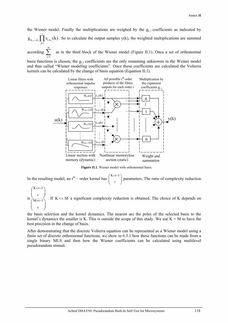
6.3 Finding Volterra kernels using Wiener model 96
6.3.1 Forming an orthonormal set of functions from a binary MLS 98
6.4 Implementation of the CAT tool 100
6.5 Simulation results 101
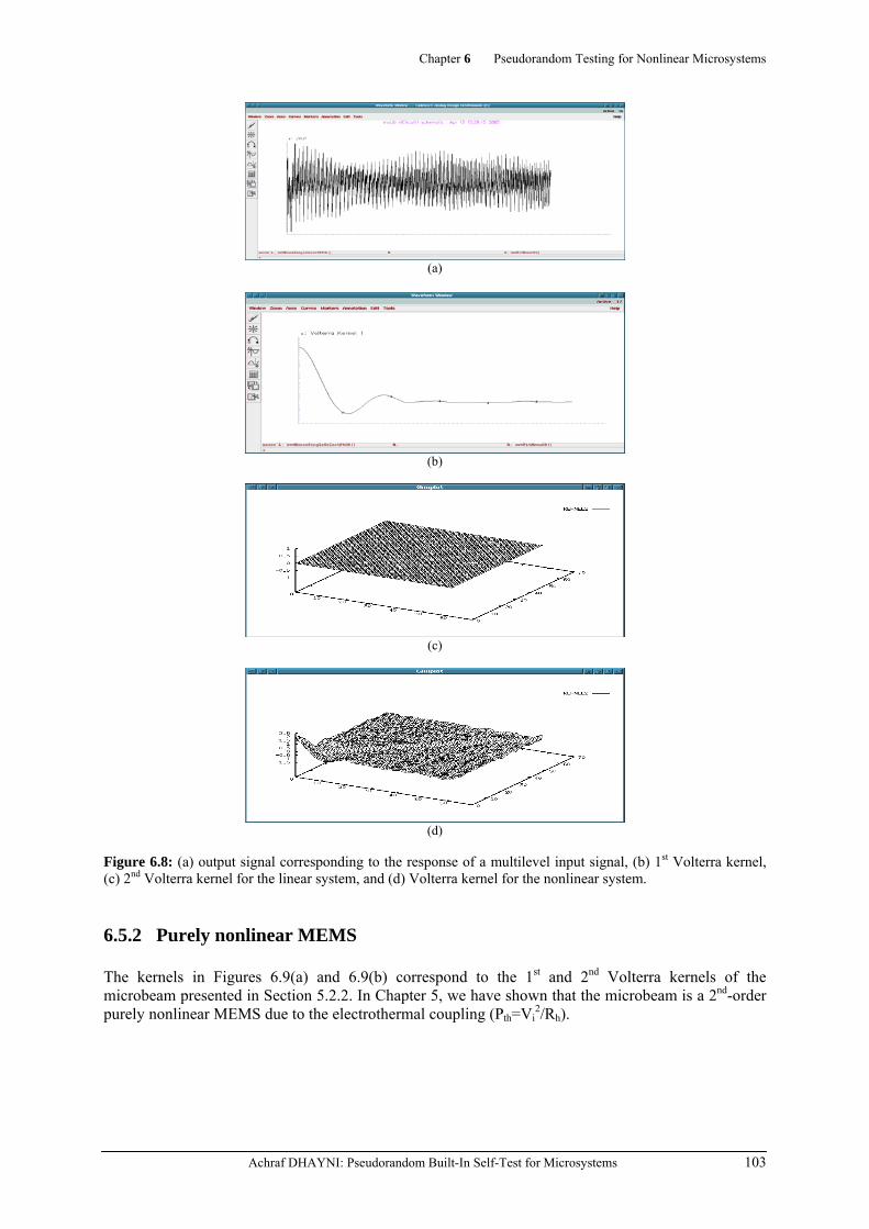
6.5.1 Nonlinear system 101
6.5.2 Purely nonlinear MEMS 103
6.6 Validity of the binary PR BIST for testing nonlinear microsystems 105
6.7 Conclusions and further work 105
Contents
Achraf DHAYNI: Pseudorandom Built-In Self-Test for Microsystems iv
Chapter 7 Conclusions and Future Work
7.1 Contributions 107
7.2 Future work 108
Publications 111
Annex I Pseudorandom Correlation Normalization 113
Annex II Volterra Kernels Expansion on Orthonormal Functions Basis 117
Annex III Multilevel Stimulus Generation 119
Bibliography 125
Abstract 133
List of Figures
Achraf DHAYNI: Pseudorandom Built-In Self-Test for Microsystems v
List of Figures
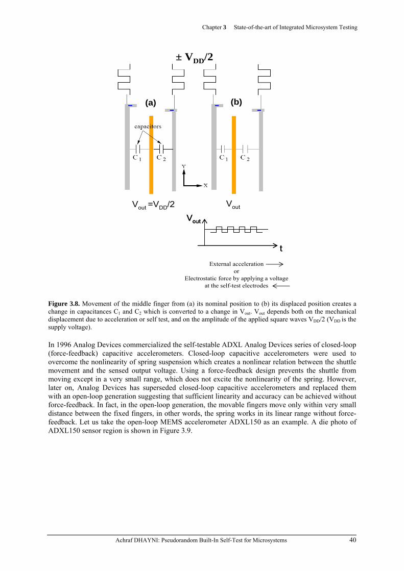
Figure 1.1. Three-dimensional view of various bulk-micromachined shapes. Figure 1.2. Illustrating surface micromachining: etching removes a sacrificial layer beneath a cantilever beam. Figure 1.3. Top 30 microsystem manufacturers versus their investments (million US dollars) in the MEMS market of the year 2004. Figure 1.4. System on-chip (a), and self-testable system on-chip (b). Figure 2.1. Gaussian distribution used to model parametric variations. Figure 2.2. Different approaches of parametric fault injection. Figure 2.3. Test input/output diagram. Figure 2.4. DSP-based block diagram. Figure 2.5. A full differential circuit with analog checkers. Figure 2.6. OBIST block diagram. Figure 2.7. OBIST with analog comparator. Figure 2.8. Histogram-based BIST technique. Figure 2.9. Histogram of (a) sinusoidal signal, (b) Gaussian random signal. Figure 2.10. HBIST block diagram. Figure 2.11. Pseudo-random BIST technique. Figure 2.12. Digital BIST for transient testing. Figure 2.13. IEEE 1149.4 mixed-signal boundary scan test architecture (a), an example of how the standard can be applied for the case of a switched capacitor filter (b), and how ABMs are used to test each filter stage alone (c). [118] Figure 3.1. Typical microsystem test flow. Figure 3.2. Catastrophic faults due to: (I) bulk micromachining defects, (a) break, and (b) insufficient etching. (II) Surface micromachining defects, (c) stiction, and (d) finger break. (III) Failure mechanisms and modes: (e) break caused by electrical overstress, and (f) Infrared emission indicates improper heating (CCD image). [51] Figure 3.3. Schematic representation of the ETC. Figure 3.4. Infrared images of the ETC during normal operation (a), and after several hours of operation (b). Figure 3.5. Some MEMS with extra elements for electrical stimulation. Figure 3.6. Manufacturing flow and test stages Figure 3.7. Topology of a typical accelerometer. Figure 3.8. Movement of the middle finger from (a) its nominal position to (b) its displaced position creates a change in capacitances C1 and C2 which is converted to a change in Vout. Vout depends both on the mechanical displacement due to acceleration or self test, and on the amplitude of the applied square waves VDD/2 (VDD is the supply voltage). Figure 3.9: (a) Die photo of ADXL150 sensor region (4x3 self-test cells and 42 sense cells), (b) enlarged view of electrodes [117]. Figure 3.10. Basic block diagram of the ADXL150 measurement system [117]. Figure 3.11. Top view of the accelerometer showing (a) the sensor with its self-test features, and (b) differential amplifier used to amplify the differential output at the sense fingers. Figure 4.1: (a) Linear IR, (b) IR corrupted by nonlinear distortion. Figure 4.2. Nonlinear system modeling: (a) frequency-domain model, (b) distributed time-domain model, and (c) lumped-time domain model.
3 4 5
6
13 14 16 18 19 19 19 20 20 20 21 21 22
25 28
30 30 36 38 39 40
41
41 42
52 54
List of Figures
Achraf DHAYNI: Pseudorandom Built-In Self-Test for Microsystems vi
Figure 4.3. Schematic representation of the measurement setup. Figure 4.4. TDS signal processing. Figure 4.5. An example of a linear sine sweep signal with initial and final frequencies at 10 Hz and 1000 Hz respectively. Figure 4.6: (a) IR using a linear sweep method, (b) IR using the logarithmic sine sweep method [137]. Figure 4.7. Nonlinear system modeling used by Farina [137]. Figure 4.8. Spectrum of a logarithmic sine sweep signal. Figure 4.9: (a) Feedback shift-register corresponding to xm+xn+1, (b) an example of the generated MLS. Figure 4.10. Fibonacci implementation of LFSR. Figure 4.11. Galois implementation of LFSR. Figure 4.12. Autocorrelation of a maximal length sequence represented by 1 and –1. Figure 4.13. Block diagram of a MLS-based measurement. Figure 4.14. Block diagram of a simplified correlation cell (SCC). Figure 4.15. Block diagram of the pseudorandom on-chip technique. Figure 4.16. IR corrupted by the indicated artifacts. Figure 4.17: (a) IR of ADXL202AQC without prefiltering, (b) zoom of (a), (c) IR with prefiltering at 50 KHz, (d) zoom of (c). Figure 4.18: (a) IRS generated by fifth order shift register, (b) first order autocorrelation of (a). Figure 4.19. Output of IRS crosscorrelation indicating anti-symmetry about L samples. Figure 4.20. Effect of averaging on IR measurement: (a) N=1, and (b) N=100. Figure 5.1. (a) Impulse response, (b) Frequency response of the ADXL103 model. Figure 5.2. Block diagram presentation of the pseudorandom technique. Figure 5.3. Impulse and frequency responses of the ADXL103 circuit using the pseudorandom impulse measurement method. Figure 5.4. Impulse and frequency responses of the ADXL103 circuit using the pseudo random impulse measurement method. Figure 5.5. Scanning Electron Microscope image of a fabricated microstructure. Figure 5.6. Behavioral model of the microstructure. Figure 5.7. Block diagram of the SCC. Figure 5.8. Hammerstein model. Figure 5.9. (a) IR of the microbeam, (b) zoom on the IR in (a), and (c) transfer function of the linear part of the model. Figure 5.10. Simulation results, (a) Range of fault-free circuits and (b) Zoom of (a). Figure 5.11. (a) Partial derivative curves of the sample amplitudes As1, As2, As3 and As4 with respect to a performance parameter P. (b) Average sample sensitivity to parameter P. Figure 5.12. (a) Sensitivity curve of the first 4 samples to the performance parameter DC gain. (b) Average sample sensitivity to the performance parameters Fm, Fth and DC gain. Figure 5.13. Emulation of the PR BIST showing the measurement of a 5-sample test signature. Figure 6.1. (a) linear system, (b) and (c) 2nd order nonlinear systems. Figure 6.2. Volterra kernels for the systems in Figure 6.1. (a) 1st kernel for all systems, (b), (c) and (d) 2nd kernels for the systems in Figure 6.1(a), 6.1(b) and 6.1(c) respectively. Figure 6.3. Wiener model with orthonormal basis. Figure 6.4. Structure of Wiener model. Figure 6.5. Volterra modeling tool user interface. Figure 6.6. Multilevel input sequence generated for Mu = 4, N = 2 and Alpha = 1. Figure 6.7. Schematic representation of a nonlinear case study. Figure 6.8: (a) output signal corresponding to the response of a multilevel input signal, (b) 1st Volterra kernel, (c) 2nd Volterra kernel for the linear system, and (d) Volterra kernel for the nonlinear system. Figure 6.9. 1st and 2nd Volterra kernels of the microbeam.
55 56 57
58 58 59 62 62 62 63 64 65 65 66 69
70 71 75
78 79 79
80
81 83 84 84 85
86 87
88
89
95 95
97 99
100 101 102 103
104
List of Tables
Achraf DHAYNI: Pseudorandom Built-In Self-Test for Microsystems vii
List of Tables
Table 1.1. Domains of microsystem applications. Table 2.1. Categories of defects and faults in analog circuit testing. Table 3.1. CMOS process and bulk micromachining defects. Table 3.2. Operational failure mechanisms and defects. Table 3.3. Richness of basic microsystems elements, basic functions constructed from elements, and multi-microsystem (Multi-MEMS) systems. Table 3.4. Categorization of past research in microsystems testing. Table 4.1. Maximum amplitude of PE = 20 dBm (10 mV), Ad = -20 dB for each order of the nonlinearity distortions. Table 4.2. Maximum amplitude of MLS =20 dB, Ad=-20 dB for each order of the nonlinearity distortions. Table 4.3. Maximum amplitude of IRS =20 dB, Ad=-20 dB for each order of the nonlinearity distortions. Table 4.4. Comparison between the PR and PE test techniques. Table 5.1. Simulation and experimental results of ADXL specifications. Table 5.2. Test quality simulation results. Table 6.1. Categories of nonlinear modeling techniques. Table 6.2. Input parameters.
2
11
29 29 31
47
61
67 71 74
81 90
92 101
List of Tables
Achraf DHAYNI: Pseudorandom Built-In Self-Test for Microsystems viii
Chapter 1 Introduction
Achraf DHAYNI: Pseudorandom Built-In Self-Test for Microsystems 1
Chapter 1 INTRODUCTION 1.1 Microsystems Miniaturization has been the most important trend for silicon technologies in the last decades. The sizes of microchips have been reduced from centimeters to micrometers resulting in a decreased size and cost of consumer electronics goods, mobile phones, etc. Today it is expected that micro sensors and actuators will develop in the same way. The successful fabrication and operation of micrometer-sized actuators and micromechanical devices provides the opportunity to produce micro miniature machines and mechanical systems. Such systems are called microsystems in Europe, Micro Electro Mechanical Systems (MEMS) in the United States, and micromachines in Japan. The silicon pressure microsensor used presently in millions of automobiles is a well-known application of microsystem technology. Also, micromachined accelerometers are used for triggering air bags and controlling active suspensions and anti-skid brakes. Microactuators are following the success of microsensors. The first major commercial application of actuators has been in camera objectives introduced by Canon in 1987. Microsystems are expected to add tremendous capabilities to microelectronics, especially in what concerns human security and health. An interesting example can be that of the project of the technical team in Sandia National Laboratory (SNL) with the collaboration of several other laboratories. Their goal is enabling certain blind people to see. The idea, funded by a $9 million project, is to design 1000 points of light through 1000 tiny MEMS electrodes. These electrodes will be placed on the retina to replace the damaged rods and cones that cause blindness. Such projects are more and more supported by the industry and expected to be commercialized in the coming few years. In addition to consumer electronics and automotive industry, microsystems are used in communications technology, chemical and environmental analysis, life science, medical technology and process industry, and even in paper making. Table 1.1 exposes the most important domains of microsystem applications. Integrating microsystem devices into a complete microsystem will be the final goal of the microsystem technology. Complete microsystems that sense, act, communicate and self-power will make life more secure, spawn new industries, and will make the revolution in biology a reality.
Chapter 1 Introduction
Achraf DHAYNI: Pseudorandom Built-In Self-Test for Microsystems 2
Defense Medical Electronics Communications Automotive
Munitions guidance Blood pressure sensor Disk drive heads
Optical or photonic switches and cross-
connects in broadband networks
Internal navigation sensors
Surveillance Muscle stimulators & drug delivery systems Inkjet printer heads RF relays, switches,
and filters Air conditioning
compressor sensor
Arming systems Implanted pressure sensors
Projection screen televisions
Projection displays in portable
communications devices and
instrumentation
Brake force sensors & suspension control
accelerometers
Embedded sensors Prosthetics Earthquake sensors Voltage controlled oscillators (VCOs)
Fuel level and vapor pressure sensors
Data storage Miniature analytical instruments
Avionics pressure sensors Splitters and couplers Airbag sensors
Aircraft control Pacemakers1 Mass data storage systems Tunable lasers “Intelligent” tires
Table 1.1. Domains of microsystem applications.
1.2 Microsystem technology In the early 60s, the history of MST began. That was when a resonant gate transistor was fabricated by researchers at Westinghouse Laboratories. The idea was to chemically etch away material to release a metal beam which could freely move. The thought of making suspended structures by a releasing process was slowly taken up in the early 70s when commercial pressure sensors appeared (based on bulk etched silicon wafers), and the first silicon accelerometer was demonstrated. Silicon surface micromachining processes based on the sacrificial layer techniques have appeared in the 80s. During this period silicon and polysilicon were recognized as important materials for micromechanical structures. Following the creation of micro-comb actuators and electrostatic micro-motors, the term “MEMS” was coined. The rotary micro-motor, despite the fact that it had little prospect of practical applications, really inspired a generation of scientists and technologists to explore many other possibilities of miniaturization, and caught the attention of the newborn MST industry. Millions of micromachined accelerometers and crash sensors were produced in 1990s. This period was the booming era for the MST development with many advances in new technologies and new applications. Many micromachining processes were developed, such as the MUMPS® process from MCNC, the Analog Devices technology and the Sandia Ultra-Planar Multilevel MEMS technology (SUMMITTM) which enabled the truly micromechanical systems [1]. MST development then followed the footsteps of the microelectronics industry and many technologies were borrowed directly from integrated circuit manufacturing processes. Nowadays, the majority of MEMS devices and products are still made of silicon or silicon forms the major material. However other materials are increasingly playing more important roles. A typical example is the development of the LIGA technology that has become a very important technology to produce non-silicon microsystems [1]. 1 An electronic device that is surgically implanted into the patient's heart and chest to regulate heartbeat.
Chapter 1 Introduction
Achraf DHAYNI: Pseudorandom Built-In Self-Test for Microsystems 3
In the following we present a brief overview of two basic microsystem technologies: bulk and surface micromachining. In bulk micromachining [2], microstructures are fabricated by etching into the wafer. Etching can be applied at the back side and/or the front side of the substrate. Bulk micromachining begins with a single-crystal wafer on which a thin film (called an etch mask because it is inert to chemical etchants) is deposited. For silicon wafers, silicon dioxide or nitride is most commonly used as the etch mask material. The film is then patterned to allow the removal of undesired portions of the film. Patterning of the etch mask film is accomplished through photolithography. Subsequently, the bulk material is etched using either wet or dry etching. Figure 1.1 shows a three-dimensional view of various bulk-micromachined shapes of the structures that can be realized with this technology. Notice how etching is applied at the front side of the substrate for the beam, the bridge, and the cavity. This is the front-side micromachining. However, back-side micromachining is employed for the membrane and the nozzle.
Figure 1.1. Three-dimensional view of various bulk-micromachined shapes.
Bulk micromachining enables the fabrication of reliable and stress-free microstructures. It is widely used to fabricate membranes, beams, cavities, and nozzles [2], as illustrated in Figure 1.1. Examples of bulk-micromachining technologies include those from Lucas Nova Sensor [2] and IBM [1]. Devices fabricated using bulk-micromachining processes include pressure and acceleration sensors [2]. However, bulk-micromachining suffers from several disadvantages such as lower dimensional control, limited capacity to interface with CMOS integrated circuits, and relatively large device sizes. Due to larger device sizes, large volume production of bulk-micromachined devices can be less economical compared to their surface micromachined counterparts [3]. Bulk micromachining is a subtractive technology and has the unavoidable characteristic of material waste associated with traditional subtractive processes. Contrary to bulk micromachining, surface micromachining [4] is an additive technology since it is based on the deposition of thin film layers on the wafer. This additive characteristic makes it agreeable to direct integration with integrated circuits. Most commercial microsystems are fabricated using surface micromachining because of the advantages it has when compared to bulk micromachining. These advantages include greater dimensional control, higher compatibility to monolithic CMOS integration, and smaller device size. Surface micromachining begins with the deposition of insulating layers (e.g., silicon nitride and oxide) followed by a sacrificial layer, which is usually an oxide material. The sacrificial layer is patterned by photolithography and etched in those regions where the microstructure will attach to the substrate. Next, the structural layers (which may include several layers of polysilicon, metal, and oxides) are deposited on top of the sacrificial layer. A key feature of a surface-micromachining process is the release step where suspended microstructures are created by etching away the underlying sacrificial layer. Figure 1.2 illustrates how a surface-micromachined device appears.
Beam
Bridge
Cavity
Nozzle
Membrane
Substrate
Chapter 1 Introduction
Achraf DHAYNI: Pseudorandom Built-In Self-Test for Microsystems 4
Figure 1.2. Illustrating surface micromachining: etching removes a sacrificial layer beneath a cantilever beam.
Examples of surface-micromachining technologies include the MEMSCAP MUMPS (Multi User MEMS Process Service) [5], Sandia National Labs SUMMiT V process [6], Analog Devices iMEMS process [7], and CMOS-MEMS [8]. Early applications of surface-micromachining include the digital mirror display [9] and the accelerometer [10]. Current commercial applications include accelerometers [11], gyroscopes [12], and micromirror optical beam steering [9]. Applications of active research include micro fuel cells [13], micro gas sensors for mass spectroscopy [14], resonator-based oscillators, mixers, and filters for IF/RF communications [15]. 1.3 Microsystem industry The MST industry has been a fast growing industry in the last decade but there were only a few big players, for example Hewlett Packard, BOSCH, EPSON, Analog Devices and Motorola. Expectations say that the main applications, within this market, will be dominated by Information Technology related peripherals, bio-medical, automotive, household appliance and telecommunications. Microsystems products and technologies have a number of attributes that make them attractive for the advanced manufacturing industry of the coming century. These advantages include:
Suitability for low cost high volume production.
Reduced size, weight and energy consumption.
The possibility to spread a large number of microsystems for distributed measurements.
Integration with control electronics.
Bio-capability.
Such attractive features are being realized by many industrial applications.
Top view Cross section
Substrate
Deposit and pattern sacrificial layer
Deposit and pattern structural layer
Release by removing sacrificial layer.
Suspended cantilever beam.
Chapter 1 Introduction
Achraf DHAYNI: Pseudorandom Built-In Self-Test for Microsystems 5
Microsystems market attained 12 billion dollars in 1996 and 34 billions in 2002. Figure 1.3 shows the top 30 microsystem manufacturers investments in 2004 [15]. Texas Instruments has become the world leader in MEMS manufacturing, with sales of 900 M$, based on sales of DLP2. Bosch is the first MEMS sensor manufacturer, with more than 90 million devices shipped in 2004 and 30% growth attained in 2005. The inertial sensor manufacturers (BEI Technologies, Analog Devices, VTI and Freescale mainly) are facing a very strong growth, due to automotive applications (strong growth of ESP3 for example) and consumer applications.
0
100
200
300
400
500
600
700
800
900
1000
Figure 1.3. Top 30 microsystem manufacturers versus their investments (million US dollars) in the MEMS market of the year 2004.
About two thirds of the market is shared by inkjet print heads and hard disk read heads. The remaining third is shared by pressure sensors, accelerometers, infrared imagers, micromirrors projection systems and biomedical microsystems. Many other microsystems are not yet massively commercialized, but of course they will be soon due to their important applications. Among these microsystems we can mention the biochips and RF passive elements. 1.4 Microsystem testing The growing use of microsystems in life-critical applications such as air-bag accelerometers, bio-sensors, pressure sensors, and satellites applications has accelerated the need for a high reliability that cannot be achieved without the use of robust test methods. However, microsystems have complex failure mechanisms and device dynamics that are not properly understood yet. This is due to the fact
2 DLP stands for Digital Light Processing: microsystem technology is used to fabricate DLP digital mirror arrays that are used to process communication signals in the optical domain. The digital mirror array is driven by a Digital Signal Processor (DSP). 3 Electronic Stability Program: electronics containing MEMS that manipulate the brakes and engine torque to prevent or reduce skids.
TEX
AS
INS
TRU
ME
NTS
HE
WLE
TT P
AC
KAR
D
RO
BER
T B
OSC
H
ST
MIC
RO
ELE
CTR
ON
ICS
SE
IKO
EPS
ON
LEX
MA
RK
BE
I TE
CH
NO
LOG
IES
AN
ALO
G D
EVI
CES
OM
RO
N
GE
NO
VAS
ENS
OR
FRE
ESC
ALE
DE
LPH
IDEL
CO
ELE
CTR
ON
ICS
DEN
SO
HO
NE
YW
ELL
INFI
NEO
N T
ECH
NO
LOG
IES
AG
VTI
TEC
HN
OLO
GIE
S
CAN
ON
OLI
VETT
I JE
T
BOEH
RIN
GER
ING
ELH
EIM
MIC
RO
PA
RTS
SIL
ICO
N S
ENSI
NG
SY
STE
MS
DA
LSA
SC
MU
RAT
A
AGIL
ENT
TEC
H
CO
LIBR
YS
MAT
SUSH
ITA
ELEC
.
INTE
RS
EM
A
ULI
S
SM
I
HL
PLA
NAR
APM
Chapter 1 Introduction
Achraf DHAYNI: Pseudorandom Built-In Self-Test for Microsystems 6
that microsystems are heterogeneous since they are based on the interactions of multiple energy domains that can include electrical, mechanical, optical, thermal, chemical and fluidic. This multi-domain nature of microsystems makes them inherently complex for both design and test. One of the most important problems that accompany the multiple energy nature is interference. The proximity of various sub-systems in an integrated microsystem can lead to adverse interference. For example, heat dissipation in a digital signal processing subsystem can lead to thermal expansion of a mechanical sensor that leads to an erroneous sensor output. Another problem is packaging. A significant barrier to economic testing of high-volume microsystems is the mechanical stresses caused by packaging. For example, stress developed in springs can change their spring constant and also result in bending (called also curvature). For a pressure sensor, the influence of package stress resembles noise and can cause undesired variations at the sensor output. In addition, the increasing number of devices integrated on chip has added to the challenge of microsystem testing. In the near future, microsystems will be imbedded within a SoC as shown in Figure 1.4. The interest behind this is to design a chip that contains diverse IP4 blocks of different technology like memories, digital circuits, analog circuits, RF circuits, antennas, and microsystems. This will reflect large benefits in terms of time-to-market shortening and design area shrinking. However, this new generation of devices poses many design and test problems.
Figure 1.4. System on-chip (a), and self-testable system on-chip (b). With the SoC approach, the interconnections are not accessible as in the case of printed circuit boards. So microsystems that were accessible to be stimulated by physical signals will be embedded, obliging test engineers to use electrical stimuli. SoC approaches are imposing new research efforts like:
Adding new pins necessary to gain access to certain inputs and outputs of the IPs to be tested. Or using a Built-In Self-Test (BIST) approach.
Adding a special test block (Figure 1.4(b)) to organize the testing process of the IPs.
In the case of BIST, the test is brought on chip and it becomes necessary to minimize the silicon area overhead.
Several standardization works have been proposed to provide a solution that allows automatic identification and configuration of testability features in ICs containing embedded cores. In particular
4 Intellectual Property.
Test
(a) (b)
(DSP)
TAM Bus
Chapter 1 Introduction
Achraf DHAYNI: Pseudorandom Built-In Self-Test for Microsystems 7
the IEEE P1500 standard which proposes an architecture of the type shown in Figure 1.4(b), requiring new considerations and design for testability (DFT) features like:
Bus for test access mechanism (TAM), see Figure 1.4(b).
Test block to manage the test data of different IPs.
Finding what must be done inside the core to simplify test integration.
The techniques of Design For Testability (DFT) like scan path, boundary-scan and Built-In Self-Test (BIST) are largely employed for digital circuits. For analog (whether electric or MEMS) and mixed-signal circuits, there are less standard approaches. A standard for analog and mixed-signal boundary scan testing is the IEEE 1149.4. On the other hand, some ad hoc BIST solutions for specific blocks exist. These approaches have so far failed to reach wide industry acceptance. 1.5 Our objectives and contribution The most promising approach to improve microsystem testability is the Built-In Self-Test approach. We focus on this point of view in the next Chapter. BIST techniques for analog and mixed signal circuits help in reducing ever increasing test related difficulties. In addition to improved manufacturing test, BIST offers an extension towards in-the-field validation and provides a promising approach to facilitate MEMS production testing and increase throughput. During the work of this thesis, we have tried to avoid the weak points of previous BIST approaches used in analog testing. The BIST technique that we propose is totally digital with a small overhead for typical case-study devices. The only connections to the MEMS under test are at the normal input and output, with no internal analog changes. The analog output must be converted to a digital signal for an on-chip BIST implementation. Moreover, our BIST is general purpose and applies a functional test which can tolerate noise, process variations, nonlinear distortion, and it can be configured to test certain nonlinear devices. Nowadays, only functional testing for MEMS is considered in industry. Structural testing for MEMS is still very difficult. This is due to the large variety of primary functional elements (e.g. cantilever beams, moving and/or twisting plates, gears, hinges, etc.) for which failure modes and fault models are often poorly understood. Our last objective was to extend the pseudorandom BIST technique to the case of nonlinear devices, and we have come out with a BIST that generates a two-level sequence stimulus for linear MEMS. For nonlinear MEMS, a multilevel stimulus is necessary, a new level for each additional nonlinearity order that must be tested. Notice also that multilevel pseudorandom sequences can be easily implemented on chip. The output test response of the MEMS under test is digitized using an Analog to Digital Converter (ADC). After that some digital signal processing is performed to evaluate Impulse Response (IR) samples for linear MEMS or Volterra kernel samples for nonlinear MEMS. According to these samples, a pass/fail signal is output by the BIST. Important advantages of this BIST technique are electrical compatibility, and high noise and distortion immunity when compared with other impulse response techniques. If an ADC is already available on chip, the BIST overhead is very small. The BIST has been applied for microsystems like microbeams, accelerometers, and microresonators. Measurements have been realized on commercial accelerometers to demonstrate the accuracy of the test approach. For the case of the microbeam, fault simulation was performed by Monte Carlo simulations and the BIST has shown excellent test metrics.
Chapter 1 Introduction
Achraf DHAYNI: Pseudorandom Built-In Self-Test for Microsystems 8
1.6 Thesis overview The rest of the dissertation is organized as follows: In Chapter 2, analog and mixed-signal testing is presented to introduce concepts which apply for microsystems as well. We first define and classify analog defects and faults. Next structural and functional analog test approaches are presented. Then we explain how a testing approach can be improved and evaluated by fault simulation and how the test efficiency is evaluated through several test metrics. This Chapter is terminated by discussing the design for testability for analog ICs. Chapter 3 presents the state-of-the-art of microsystems testing by discussing the current practices in microsystem testing, failure mechanisms and defects, fault modeling and fault simulation, the importance of built-in self-testing in microsystem applications, the BIST capabilities that have appeared in commercialized MEMS, and test practices for MOEMS and RF MEMS. Finally a categorization of almost all past research in the domain of microsystem testing forms the summary of this Chapter. Chapter 4 explores the techniques of signal processing for measuring the IR of Linear Time-Invariant (LTI) systems. These techniques are classified according with their complexity (i.e. the overhead that they cause) for a BIST implementation and whether they need the on-chip presence of a Digital Signal Processor (DSP) or not. A detailed comparison between the different techniques is performed. Through this comparison the pseudorandom test methods will prove high suitability for BIST implementation, and good immunity to noise and nonlinear distortion. After proving the efficiency of the pseudorandom technique and its suitability to be implemented in a BIST environment, the PR BIST is applied to two case studies in Chapter 5. The Chapter begins by applying the PR technique to characterize a commercialized accelerometer in its linear range and, then, to characterize and test a microbeam (cantilever) that has a nonlinear behavior due to the way it is stimulated. For the case of the nonlinear microbeam, the BIST approach has been exemplified. BIST parameters (LFSR length, ADC and cross-correlation precision and number of samples to calculate) have been optimized using a statistical analysis while keeping test metrics such as yield loss and defect level down to few ppms5. Chapter 6 presents an extension of the PR test approach to the case of nonlinear devices. A CAT (Computer Aided Test) tool has been developed. This tool allows characterizing and testing nonlinear devices by identifying the Volterra kernels. The generation of a special kind of multilevel pseudorandom stimuli is presented. They are special because they are adapted to simplify signal processing for finding Volterra kernels. Volterra kernels are functions that describe the behavior of a system. The 1st Volterra kernel describes the linear behavior (it is analogous to the impulse response in linear systems), the 2nd Volterra kernel describes the 2nd order nonlinear behavior, and so on for higher order kernels and higher order nonlinear behaviors. Finally we discuss the implementation of this technique in a BIST environment, and the need for such BIST. Chapter 7 summarizes the thesis, draws conclusions and presents ideas for future work in the microsystem test area.
5 ppm: Parts Per Million, a measure for tiny quantities, usually used instead of percent.
Chapter 2 Analog and Mixed-Signal Testing
Achraf DHAYNI: Pseudorandom Built-In Self-Test for Microsystems 9
Chapter 2 ANALOG AND MIXED-SIGNAL DESIGN-FOR-TEST 2.1 Introduction Analog and mixed-signal testing is presented in this Chapter in order to introduce concepts which apply for microsystem testing as well. Microsystem testing includes all fabrication and test difficulties already defined for analog ICs. That is because microsystems are analog too, and because they may experience the same manufacturing process as analog ICs. This is typically the case for CMOS compatible microsystems. Moreover, microsystems experience a micromachining phase which, in its turn, adds more failure mechanisms to render microsystem fabrication and test more complex than analog ICs. In this Chapter, we first define and classify analog defects and faults. Next structural and functional analog test approaches are presented. Then we explain how a testing approach can be evaluated and improved by fault simulation and how the test efficiency is assessed through several test metrics. This part is terminated by discussing the design for testability for analog and mixed-signal ICs. 2.2 Analog defects and faults In the research for a reliable test technique, intuitively, one must start by searching the failure mechanisms that cause defects in the fabricated circuit. Then the research continues to discover how defects can affect the functionality of the circuit by assigning the faults that correspond to each defect. Once we have all possible faults in our hands, we can start to look for the test technique capable of detecting these faults. For this purpose, the ideal design of the circuit under test (CUT) and the fault models must be ready for fault injection. During fault simulation, faults are injected to the ideal circuit electric model and the test technique is verified and evaluated. In a circuit, defects are physical imperfections induced by failure mechanisms during fabrication and when the circuit is in service. Defects are totally related to the fabrication processes and the type of functionality that can be imposed to the DUT when in service. So, to define the possible defects, both the fabrication technology and the DUT functionality must be taken into consideration. Defects can cause faults in the functionality and lead to faulty circuits. Here test can intervene to detect faults and discriminate fault-free from faulty circuits. Defects and faults are almost synonymous, one means the other. However there can be some defects that do not show up as faults. This kind of defects impacts the reliability during operation. For digital circuits the “stuck-at” fault model has been shown to be representative of the most likely defects, especially for CMOS processes. Typical faults for digital circuits include: stuck at 1, stuck at 0, stuck open, stuck on, delay faults, short circuits between adjacent lines (bridges) and open circuits.
Chapter 2 Analog and Mixed-Signal Testing
Achraf DHAYNI: Pseudorandom Built-In Self-Test for Microsystems 10
In the last decade, other fault models have been found for delay and IDDQ6 faults. According to this
simple fault model list, digital device testing has been efficiently solved with general purpose methods like scan path [16, 17], boundary-scan (IEEE 1149.1) [18] and BIST [19-21]. Fault coverage is an accepted measure of the quality of a digital circuit test, and is defined as the percentage of possible faults that can be detected by a given test. Fault coverage for analog circuits has been simply defined in [37, 45] as the percentage of the number of potential shorts and opens (catastrophic faults that cause a complete malfunction) that can be detected by a test. However, for analog circuits, parametric variations must be considered as well. It is impossible to fabricate always the same circuit, the design parameters vary from one fabricated circuit to another. Parametric variations (also called parametric deviations and process deviation) are acceptable as long as each parameter varies within its specified interval of tolerance (specification). Ideally, if at least one parameter deviates more than its tolerance range, the fabricated circuit is out of specifications and should not be shipped to the market. Parametric variations are “global” when they arise due to statistical fluctuations in the parameters of the fabrication process. For example, these parameters can be: oxide layer thickness, doping, line width, and mask misalignment. Parametric variations are “local” when they arise due to statistical fluctuations in some physical or geometrical parameters of some elements in the circuit. In both cases, parametric variations are generally modeled as a Gaussian random variable with a mean equal to the nominal value of the parameter, and a standard deviation σ which expresses the tendency to deviate from the nominal value according to the Gaussian distribution law. More details are presented in the analog fault modeling section (Section 2.4). Parametric variations are the major source of concern for most analog test engineers. That is because catastrophic defects, like shorts and opens, lead to catastrophic faults of easily detected performance failures (e.g. no signal output at all). On the other hand parametric variations impact the functionality by adding a certain error to any of the physical or geometrical circuit parameter. And then it is the duty of the testing technique to decide whether this impact is harmful or not. The impact is harmful if the circuit is out-of-specifications (out-of-spec). Notice that we use the terms “faulty” and “faulty-free” to designate, respectively, bad and good circuits relative to catastrophic defects. However we use the terms “out-of-spec” and “within-spec” to designate, respectively, bad and good circuits relative to variation parameters. The difference between a faulty and an out-of-spec circuit is that the out-of-spec circuit does not have a complete malfunction and that is why its test is more complicated. An out-of-spec analog amplifier may continue to amplify with a certain error in its gain for example, but when it is faulty, no amplification function exists. Of course, an ideal test technique must pass all fault-free and within-spec circuits (these are the good circuits) and must reject all faulty and out-of-spec circuits (these are the bad circuits). Some circuits that are marginally out-of-spec can escape the test to be classified as within-spec instead of out-of-spec circuits. These are the “test escapes” leading to a “false acceptance”. On the other hand, some circuits that are marginally within-spec risk to fail the test and to be classified as out-of-spec instead of within-spec circuits. The number of these circuits defines the “yield loss” and “false rejection”. Test escapes, false acceptance, yield loss, false rejection and others are important metrics used to evaluate the efficiency of test techniques. More details are presented in Section 2.5.
6 Iddq testing is a method for testing CMOS integrated circuits for the presence of manufacturing faults. It relies on measuring the supply current (Idd) in the quiescent state (when the circuit is not switching). The current consumed in the state is commonly called Iddq for Idd (quiescent) and hence the name. Iddq testing uses the principle that in a correctly operating CMOS digital circuit, there is no static current path between the power supply and ground, except for a small amount of leakage. Many common semiconductor manufacturing faults will cause the current to increase by orders of magnitude, which can be easily detected. This has the advantage of checking the chip for many possible faults with one measurement.
Chapter 2 Analog and Mixed-Signal Testing
Achraf DHAYNI: Pseudorandom Built-In Self-Test for Microsystems 11
Table 2.1 is a list of the kinds of manufacturing process defects and faults [24]. The rows correspond to the manufacturing process defects and the columns correspond to the impact (that can be a fault or not) of the defect on the performance of the DUT. The categories of faults and defects can then be defined as follows:
Fault (effect)
Defect (cause)
All performances within specification limits
Marginally out-of-spec performance
(parametric fail)
Faults that cause complete malfunction
Process parameters within spec limits Defect-free and fault-free A2 A3
Process parameter out of spec limits (locally) B1 B2 B3: Seriously out-of-spec
performance
Shorts and opens C1 C2 C3: Catastrophic fault (faulty circuit)
Table 2.1. Categories of defects and faults in analog circuit testing.
A2: A local or global process deviation, or combination of deviations, within process specifications that causes a circuit performance to fail. In theory, these faults should not occur because if all process parameters are within specification (within their intervals of tolerance), then certainly the circuit will function correctly. However, in reality, a designer can never be sure that his circuit must work correctly if all process parameters are within their intervals of tolerance. That is because he cannot simulate all possible process parameter combinations. A3: A local or global process deviation, or combination of deviations, within process specifications that causes a circuit to fail to function. These faults should not occur and are in fact very rare. If they occur, they are due to a mistake in the design. B1: A most probably local process deviation that is outside the process specifications but does not cause any performance to fail its specification. This type of defect might eventually cause an operational failure and thus poses a reliability risk. B2: A local process deviation that is outside the specified process limits and causes a performance to fail a specification. This category includes classic parametric faults, such as an excessive capacitance causing the bandwidth to be insufficient. B3: A local process deviation that is outside the specified process limits and causes a circuit to fail to function. This can occur, for example, when some threshold is involved, such as a low (or high) VT (voltage threshold) causing a transistor to not turn off (or on). C1: Any short or open circuit (i.e. that changes the circuit topology) without causing any performance to fail its specification. This can occur due to redundancy or unspecified performances. For example, power supply rejection ratio is not always specified. Another example is a resistive short circuit that causes excessive current in a metal line, but the circuit remains within specification because of test specifications are not violated. These kinds of faults can reduce reliability. C2: Any short or open circuit that causes a performance to marginally fail a specification. An example is a bias chain of transistors, one of which is shorted, causing excessive drain current (IDD). C3: Any short or open circuit that causes a circuit to fail to function. This category includes classic catastrophic faults.
Chapter 2 Analog and Mixed-Signal Testing
Achraf DHAYNI: Pseudorandom Built-In Self-Test for Microsystems 12
2.3 Structural and functional test approaches Structural and functional test approaches were first defined in the world of digital testing. In digital circuit testing, digital test vectors are generated and applied to the input of the circuit under test, and then the corresponding response vectors are checked up by comparing them with the nominal (that corresponds to a good circuit) response vectors. If at least one of the output vectors is incorrect then the circuit is faulty. In functional testing, the DUT must be tested for all its possible functionalities (i.e. for all possible inputs) which is unpractical for complex digital circuits. For example, for a combinatory circuit that has n inputs we need 2n test vectors to test it and for a sequential circuit of m delay registers and n inputs we need 2n+m test vectors. Knowing that in these days there can exist digital circuits with more than 100 digital inputs, we understand the necessity to limit the number of test vectors. For the above reason, structural testing techniques have appeared for digital circuits to reduce the number of test vectors. Structural testing does not stimulate all the possible functionalities of the DUT as the functional test does, but stimulates the possible faults that can happen to the circuit like stuck at 1, stuck at 0, stuck open, stuck on, delay faults, short circuits between adjacent lines (bridges) and open circuits. In digital testing, structural testing has proved higher efficiency than functional testing. But this is at the expense of more complexity that arises from the heavy algorithms of fault simulation. These algorithms are needed to search the minimum set of test vectors (minimum test time) necessary to detect as much faults as possible (fault coverage). In general, this does not pose a problem because for a certain design the algorithm is applied only once. For analog and mixed-signal circuits, structural testing is more complicated. In digital testing it is generally enough to consider catastrophic faults (delay faults are recently being considered). But in analog and mixed-signal testing, parameter variations must be considered as well. This complicates the generation of a fault list, and poses new problems for fault modeling and simulation. Functional testing is a usual practice in analog and mixed-signal structural testing. On the other hand, functional testing is performed by verifying some representative design specifications like the gain, cutoff frequency, role-off factor, phase delay, resonance frequency, quality factor, sensitivity, signal to noise ratio (SNR), total harmonic distortion (THD), etc. Upon testing, if at least one design parameter is outside its tolerance range then the circuit is out of specifications (out-of-spec) and must be discarded from shipment to the market. 2.4 Analog fault modeling and fault simulation Given a certain technology, defects can be named and classified according to Table 2.1. Once the defect list is formed, the fault list is defined and faults can be modeled. During fault simulation, fault models are injected one by one to the nominal DUT model. At each fault injection the test stimulus is applied and the output test response is analyzed by the simulator. According to this analysis, the injected fault is either detected or not. Finally, the fault coverage is the percentage of the detected injected faults with respect to the total number of injected faults. So by fault modeling we can evaluate the efficiency of our test technique. Fault modeling is also useful to improve the quality of test stimuli to raise the estimated fault coverage. Analog fault injection may require the injection of the computationally efficient and relatively simple models of catastrophic faults as in the well-known case of digital circuits. However, for analog circuits, the most important issue is fault modeling and injection of faults caused by parametric variations. Usually it is sufficient to inject parametric variations because they dominate catastrophic faults. A fault “dominates” another fault when detecting that fault necessarily detects the other.
Chapter 2 Analog and Mixed-Signal Testing
Achraf DHAYNI: Pseudorandom Built-In Self-Test for Microsystems 13
According to the fabrication process, a process parameter (physical or geometrical) may deviate from its nominal value. This deviation is considered a fault when it goes beyond the assigned tolerance range. The parameters that are chosen frequently are, for transistors (independent parameters) [24]: zero back-bias threshold voltage Vto, effective width We, effective length Le, junction capacitance Cj, current factor β, and oxide thickness tox. Cox for capacitors. And RSH (sheet resistance) for resistors. A deviation in tox, for example, is always considered as a global process deviation since the oxidation phase is applied through all the circuit at the same time. In the processing/layout space, parameters typically deviate from the nominal value according to a Gaussian probability density function as shown in Figure 2.1.
Figure 2.1. Gaussian distribution used to model parametric variations.
In the above stochastic fault model, the value of the standard deviation σ is chosen according to the precision of the fabrication process. Large standard deviations represent a bad fabrication process where the probability of fabricating an out-of-spec circuit is high. This probability is equal to the area under the curve outside the tolerance range. Vice versa for small standard deviations, the bell shape of the Gaussian law gets narrower and the peak point gets higher, and thus the probability of fabricating an out-of-spec circuit is lower. For the case where the interval of tolerance is equal to 6σ, it can be proved that 99.73 % of the generated circuits are within the interval of tolerance. Similarly for 3σ, about 86.63 % are within the interval of tolerance. Standard deviation of 3σ and 6σ are often used to model the variation of parameters [25, 26]. Since there are an infinite number of parameter values, Monte Carlo simulations [27] are used to generate circuits with parametric variations. The near-to-reality simulations (nominal case) are when each parameter is represented by its nominal probability density function as in Figure 2.1. For fault injection, keeping the Gaussian distribution is considered necessary — intuitively, when an error arises in the fabrication process, even if some parameters deviate from their nominal value, these parameters will continue to follow a Gaussian distribution. Several works exist on the injection of parametric faults. In [25] the authors propose to vary only one parameter by introducing a shift of 3σ (interval of tolerance) to its nominal value (Figure 2.2(a)). Then Monte Carlo simulations are executed to generate randomly a large number of circuit instances. For the parameter to which faults are injected, the random generation is done according to the fault model of Figure 2.2(a). However, for all the other parameters, the random generation is done according to the nominal distribution of Figure 2.1. In [26] fault injection is simply performed by replacing the nominal Gaussian model by the nominal value plus Nσ (Figures 2.2(b) and 2.2(c)). So, Monte Carlo simulations are executed similarly as in [25] except for the parameter of fault injection that keeps a fixed value equal to its nominal value plus Nσ. Usually N is chosen to be equal to 3 or 6.
σ
Mean = nominal value
Parameter values
Probability
Chapter 2 Analog and Mixed-Signal Testing
Achraf DHAYNI: Pseudorandom Built-In Self-Test for Microsystems 14
Figure 2.2. Different approaches of parametric fault injection.
The above listed methods have been proposed to generate a large number of faulty circuits during an acceptable fault simulation time. This is important to calculate, with a ppm precision, test metrics such as false acceptance (test escapes) and rejection (yield loss). However we cannot carry out an estimation of the test quality by applying these methods because, during manufacturing, a parametric variation does not occur because of a change in the nominal value or the probability density function of a certain process parameter. However, it occurs simply because the value of the process parameter is outside the affected tolerance range. In [34], a method to calculate test metrics under process deviations is presented. A relatively small number of circuits are generated to derive the mean and variance of the Gaussian probability density function of each design parameter. Then, a large population of circuits is statistically generated by considering their design parameters as random variables which have the already calculated mean and variance. In parallel with this multi-normal (or multi-Gaussian) generation of a circuit population, test parameters are calculated, and the values that correspond to fault-free and faulty circuits are assigned in both specification and test spaces, and finally test metrics can be calculated with a ppm precision. 2.5 Test metrics Digital manufacturing test quality has been precisely assessed (until IDDQ and delay faults became a concern) by quantitative metrics of fault coverage and defect level. Direct application of these digital concepts to analog circuit test results in a poor representation of complex analog effects. Defining analog fault coverage as the percentage of shorts/opens detected by the test is clearly a poor representation of fault coverage, since the universe of faults must include parametric faults. As
Mean = nominal value Parameter values
Probability 3σ
Mean = nominal value Parameter values
Probability 3σ
Mean = nominal value Parameter values
Probability 6σ
(a)
(b)
(c)
Chapter 2 Analog and Mixed-Signal Testing
Achraf DHAYNI: Pseudorandom Built-In Self-Test for Microsystems 15
presented in the previous Section, parametric faults are significantly more important, especially since they are harder to detect, and it has been shown [28] that they dominate shorts and opens. However, since these faults span a continuous range of values, they cannot be “counted” like the number of shorts/opens can. With a statistically-based definition of parametric faults, it becomes possible to have precise and meaningful definitions for analog parametric test metrics. Three values are considered essential to evaluate the efficiency of analog test methods [24]:
1) Yield Y:
nspeci
i 1
Number of fault free circuitsYTotal number of circuits
(1 p )=
−=
= −∏ (2.1)
where n is the number of potential faults, and pispec is the probability for fault i to occur.
2) Test yield YT:
T
mtestj
j 1
Number of circuits that pass the testYTotal number of circuits
(1 p )=
=
= −∏ (2.2)
where m is the number of potential faults detected by the test, and pjtest is the probability of fault j to
occur and to be detected by the test.
3) Gp: probability of a device being fault-free and passing the test.
p
mspec testi j
i 1
Number of fault free circuits that pass the testGNumber of fault free circuits
(1 max(p ,p ))=
−=
−
= −∏ (2.3)
where n is the number of potential faults.
We can define all test metrics in terms of these three probabilities:
Yield coverage YC Yield coverage has been defined [29] as the probability that a fault-free device passes the test. This is an essential parameter from an economic and manufacturing point of view. Less than 100% yield coverage means that fault-free devices are failing the test and hence do not generate revenue. Yield coverage YC, and a related term, yield loss YL (called also probability of false rejection), are given by:
pC
GPr obability (fault free circuit & passes the test)YPr obability (circuit is fault free) Y
−= =
− (2.4)
L CY 1 Y= − (2.5) Yield coverage should not be confused with Yield. Yield is the proportion of fault-free devices out of the total population manufactured, and can only be measured by testing circuits for all specifications over all conditions, which is typically far too time-consuming to be practical. Test Yield is often used
Chapter 2 Analog and Mixed-Signal Testing
Achraf DHAYNI: Pseudorandom Built-In Self-Test for Microsystems 16
as an estimate of Yield, but if the fault coverage of a test is less than 100%, faulty devices may artificially drive up the test yield causing it to be a deceptive measure.
Defect level (test escapes) D Defect level is the proportion of defective devices in those that pass the test. This is an important measure of the quality of a test, from an economic and customer point of view. Defect Level D is commonly defined as:
p p C
T T T
Number of faulty circuits that pass the testDTotal number of circuits that pass the testPr obability (circuit is faulty & passes the test)
Pr obability (circuit passes the test)G YG YY1 1 1Y YY Y
=
=
= − = − = −
(2.6)
For the estimation of the test metrics, it is necessary to know all different types of catastrophic and parametric faults that can occur in the circuit. A practical approach to consider parametric faults has been defined in [24]. A more general but time consuming approach for considering parametric faults is to perform Monte Carlo simulations. The test metrics are then estimated according to Figure 2.3 and Equations 2.1, 2.2 and 2.3.
Test
Fail circuits
Pass circuits
n circuits to be tested
n1 pass fault-free circuits
n2 pass faulty circuits
n3 fail fault-free circuits
n4 fail faulty circuits
Figure 2.3. Test input/output diagram. Y, YT, and Gp can then be calculated as follows:
1 3n nYn+
= (2.7)
1 2T
n nYn+
= (2.8)
1p
1 3
nGn n
=+
(2.9)
Then all the test metrics can be calculated since they are all functions of Y, YT, and Gp. In this work, we will use as test metrics the concepts of false acceptance Fa and false rejection Fr defined as follows:
2a
nNumber of faulty circuits that pass the testFTotal number of circuits n
= = (2.10)
Chapter 2 Analog and Mixed-Signal Testing
Achraf DHAYNI: Pseudorandom Built-In Self-Test for Microsystems 17
3
rnNumber of fault free circuits that fail the testF
Total number of circuits n−
= = (2.11)
We notice that these definitions are different to the conditional probabilities mostly used for these concepts. 2.6 A brief description of mixed-signal BIST For many decades, mixed-signal integrated circuits (ICs) have been tested successfully through conventional testing approaches. But with more and more mixed-signal circuits integrated into complex application-specific ICs SoCs, companies no longer can afford to rely on conventional methods for testing mixed-signal ICs. Faced with more complex testing challenges, many designers and test engineers are looking for a mixed-signal design-for-test (DFT) solution to help them gather the advantages that their digital counterparts enjoy today.
Digital Built-In Self-Test (BIST) now is economical and, in many cases, the only practical way to get a product to market quickly and cost effectively. As semiconductor technology enables larger gate counts, more mixed-signal circuits are being integrated into ICs. These ICs contain hundreds of thousands of logic gates that are designed using a high-level hardware description language such as Verilog or VHDL.
The lack of automation for test development for mixed-signal circuits is the main cause behind the lack of maturity of mixed signal DFT when compared with digital DFT. For this reason, test development for mixed-signal circuits has been a major bottleneck in improving time-to-market, decreasing test costs, and increasing test performance. New breakthroughs in mixed-signal BIST, however, provide the opportunity to remove this bottleneck and streamline the test development process.
Designing mixed-signal ICs for testability can simplify and accelerate design debug and characterization. It can enable more economical testing through the use of lower-cost testers or faster tests. Also it enables performance monitoring, better diagnostics, quality and yield improvement, and yield management.
Many issues, however, have prevented the widespread adoption of any single mixed-signal DFT style. New digital compatible analog BIST solutions are emerging to address these issues. 2.6.1 Ad-hoc BIST techniques Today, the most common approach to mixed-signal DFT is ad hoc. Many companies have developed their own application-specific ways to improve testability, including adding special function modes and instructions, increasing the number of output and input pins, and providing internal loops. These methods occupy a small area on the IC and have minimal impact on performance.
A notable ad hoc method is the loop-around [31] which has been used in telecommunications ICs for many years, both at the IC and board level. The loop-around method exploits the presence of a transmitter or analog-to-digital converter (ADC) together with the complementary receiver or digital-to-analog converter (DAC). The limitations to this approach like gain and noise masking, crosstalk, and lack of diagnostic capability result in a test that is not sufficiently comprehensive.
Chapter 2 Analog and Mixed-Signal Testing
Achraf DHAYNI: Pseudorandom Built-In Self-Test for Microsystems 18
On-chip analog buses [30] are common and were discussed in publications in the mid-1980s. Analog buses are still somewhat ad hoc in nature. The choice of signals to monitor requires understanding the impact of loading on the monitored signals, the diagnostic value of the signals, crosstalk, and the impact of the limited bandwidth of the bus.
Off-chip monitoring of the internal analog signals of an IC almost always impacts its performance. The off-chip version of the signals inevitably has more noise and distortion, leading to a reduction in fault coverage or yield. Nevertheless, the approach has potential for being a methodical test access, especially if it becomes a standard. 2.6.2 Some basic BIST techniques A more complex technique is the DSP-based BIST. Figure 2.4 presents its block diagram. The Digital Signal Processing (DSP) block is responsible of signal generation and processing by means of Discrete Fourier Transform (DFT) which can be calculated using the Fast Fourier Transform (FFT). Implementing an FFT calculator is a very critical feature since it increases drastically the complexity of the BIST circuitry. The minimum FFT precision needed in test applications can not be less than 64 points. Even 64 points are not sufficient for noisy DUT. In this case, we can employ either time domain averaging at the output of the DUT to get rid of noise or frequency domain averaging of the calculated FFT.
Figure 2.4. DSP-based block diagram.
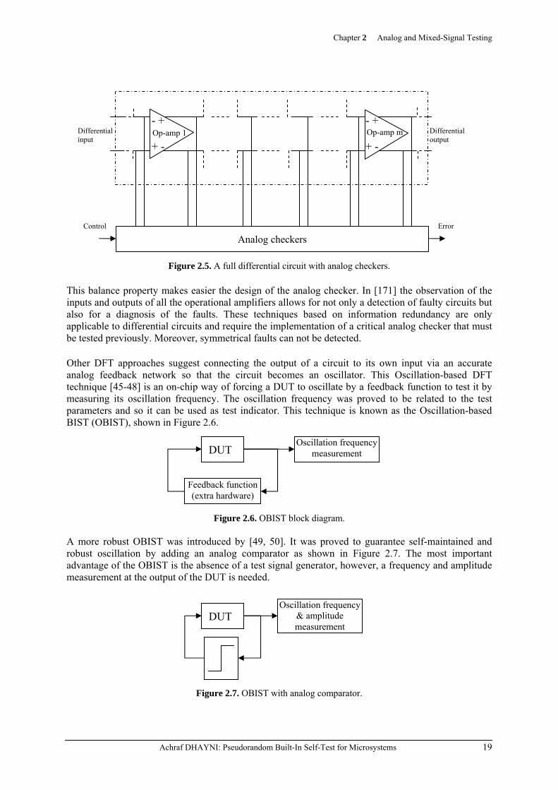
Some methods have taken advantage of the information redundancy in the fully differential circuits [166-69]. In a fault-fee differential circuit, each node pair (positive V+ and negative V− nodes) follows a Differential Analog Code: V+ + V− ≈ 2 VBIAS, where VBIAS is the common bias voltage of the nodes. A fault in the circuit may destroy this property, and by means of an analog checker (Figure 2.5), we can detect the faulty circuits. This technique allows for an on-line test, but the design of the checker is quite difficult because V+ and V− can take a broad range of values. This problem can be overcome if we observe in the circuit just the inputs of the operational amplifiers [168, 170]. If the circuit is fault-free, both inputs of the operational amplifiers ought to be close to virtual analogue ground: V+≈V−≈VBIAS.
ADC DSP
DUT
DAC
Chapter 2 Analog and Mixed-Signal Testing
Achraf DHAYNI: Pseudorandom Built-In Self-Test for Microsystems 19
Figure 2.5. A full differential circuit with analog checkers.
This balance property makes easier the design of the analog checker. In [171] the observation of the inputs and outputs of all the operational amplifiers allows for not only a detection of faulty circuits but also for a diagnosis of the faults. These techniques based on information redundancy are only applicable to differential circuits and require the implementation of a critical analog checker that must be tested previously. Moreover, symmetrical faults can not be detected.
Other DFT approaches suggest connecting the output of a circuit to its own input via an accurate analog feedback network so that the circuit becomes an oscillator. This Oscillation-based DFT technique [45-48] is an on-chip way of forcing a DUT to oscillate by a feedback function to test it by measuring its oscillation frequency. The oscillation frequency was proved to be related to the test parameters and so it can be used as test indicator. This technique is known as the Oscillation-based BIST (OBIST), shown in Figure 2.6.
Figure 2.6. OBIST block diagram.
A more robust OBIST was introduced by [49, 50]. It was proved to guarantee self-maintained and robust oscillation by adding an analog comparator as shown in Figure 2.7. The most important advantage of the OBIST is the absence of a test signal generator, however, a frequency and amplitude measurement at the output of the DUT is needed.
Figure 2.7. OBIST with analog comparator.
DUT
Oscillation frequency & amplitude measurement
DUT
Feedback function (extra hardware)
Oscillation frequency measurement
Differential input
Analog checkers
- + + -
- + + -
Op-amp 1 Op-amp m
Control Error
Differential output
Chapter 2 Analog and Mixed-Signal Testing
Achraf DHAYNI: Pseudorandom Built-In Self-Test for Microsystems 20
The Histogram-based Analog Built-In Self-Test (HABIST) [41-43] for Analog-to-Digital Converters (ADCs) is a technique that has been recently commercialized. It was firstly proposed by [41]. Its block diagram is shown in Figure 2.8. The test signal can be a sinusoidal, ramp, pulse, random, etc. If the ADC has N bits the number of possible codes is 2N. As in the case of the pseudo-random BIST, once the histogram of the output sequence is obtained it is compared with certain on-chip saved boundaries in the histogram space. Two examples of this are shown in Figure 2.9. According to this comparison, a test decision is done. The advantage of this method is that it permits on-line testing since data can be collected while the DUT is functioning.
2.6.3 BIST techniques using pseudorandom stimuli Another DFT approach is the Hybrid Built-In Self-Test (HBIST) that was introduced by [33] in 1991. It is a technique inspired from digital BIST techniques. Figure 2.10 shows the block diagram of the HBIST. The Linear Feedback Shift Register (LFSR) generates a maximal length sequence MLS which is manipulated and transformed into an analog signal by a DAC. The response of the DUT is then digitized by an ADC and compacted by means of a Multi-Input Signature Register MISR. The obtained register is finally compared with the optimal one and thus a test decision is done. This technique needs the presence of on-chip self-testable ADC and DAC. Another disadvantage is the high sensitivity to noise.
Figure 2.10. HBIST block diagram.
Another DSP-based BIST technique depends on the calculation of the Impulse Response (IR) of the DUT. It is called pseudo-random BIST because the used stimulus is a pseudo-random signal. Its block diagram is shown in Figure 2.11.
Figure 2.8. Histogram-based BIST technique.
Figure 2.9. Histogram of (a) sinusoidal signal, (b) Gaussian random signal.
Signal generator
DUT ADC
Occurrence
Amplitude
Histogram code
(a) (b)
Linear feedback
shift register Pattern
manipulator DAC DUT ADC MISR Compacted signature
Analog test pattern generation Output response analysis
Chapter 2 Analog and Mixed-Signal Testing
Achraf DHAYNI: Pseudorandom Built-In Self-Test for Microsystems 21
Figure 2.11. Pseudo-random BIST technique.
The pseudo-random signal is an MLS generated by means of a Linear Feedback Shift Register. Sufficiently long MLSs are known to have an autocorrelation almost equal to an impulse. The equation below shows how the impulse response h(k) can be derived from the DUT input/output crosscorrelation.
( )xy
xx
φ (k) = y(k) * x(-k)
= h(k) * x(k) * x(-k)= h(k) * φ (k)
(2.12)
Notice that if the autocorrelation xxφ (k) is an impulse then xyφ (k) = h(k) . So for the case of a long MLS, the input/output crosscorrelation can be considered as a good approximation of the impulse response of the DUT. Pseudo-random BIST techniques have been applied to analog and mixed signal circuits in the past [34-36]. A simple design crosscorrelation block where only the IR samples needed to form the signature are calculated has been proposed in [143, 144]. Once the signature is obtained, it is compared in the signature analysis block with certain on-chip saved boundaries in the signature space. If the obtained signature is inside these boundaries the DUT is fault-free, otherwise the DUT is classified as faulty. A simple BIST based on MLS stimulus has been proposed in [39, 40]. The digital signal processing is eliminated and only a transient testing is carried out as shown in Figure 2.12. At the output of the comparator a digital signature is formed and compared. This technique is very simple to be implemented on-chip since the generation and analysis are digital and due to the absence of the on-chip self-testable ADC needed by the techniques explained before. However, this method is very noise sensitive and checks only the transient response of the DUT.
Figure 2.12. Digital BIST for transient testing.
2.6.4 Other BIST techniques Many other analog DFT approaches have been proposed, but most require reconfiguration of the circuit under test. For example, some approaches propose that internal operational amplifiers be
LFSR DUT ADC
Cross correlation
xy (k)φ
Signature analysis
x(k) y(k) u(t)
LFSR DUT + _
Digital signature
Vref fs
MLS
Decision Faulty or faulty-free circuit
Chapter 2 Analog and Mixed-Signal Testing
Achraf DHAYNI: Pseudorandom Built-In Self-Test for Microsystems 22
converted into unity gain amplifiers and cascaded for testing all amplifiers at once or reconfiguring selected op-amps to provide serial access. Many other BISTs were proposed like: Lissajous-based BIST [44], pole-zero cancellation BIST [52] and adaptive filter BIST [53] for testing of analog filters, BIST based on measuring the state variables of the DUT [54], etc. 2.7 IEEE 1149.4 mixed-signal boundary scan test architecture The IEEE P1149.4 standard for a mixed-signal test bus uses an input and output analog bus to access analog pins (and optionally, internal nodes) of an IC (Figure 2.13(a)). IEEE P1149.4 (known as dot 4) is analogous to IEEE P1149.1 used in the digital world. The standard primarily is aimed at improving board testability by facilitating measurement of simple passive and active components on the board without a bed-of-nails tester. Dot 4 has become popular and it is commercialized by several companies and now an advanced version (IEEE P1149.6) has just come out.
(a)
(b) (c)
Figure 2.13. IEEE 1149.4 mixed-signal boundary scan test architecture (a), an example of how the standard can be applied for the case of a switched capacitor filter (b), and how ABMs are used to test each filter stage alone (c). [118]
Chapter 2 Analog and Mixed-Signal Testing
Achraf DHAYNI: Pseudorandom Built-In Self-Test for Microsystems 23
Many references explain in details the functionality of the IEEE 1149.4 mixed-signal boundary scan and test bus. To understand the idea in general, let us take an example of a 6th order bandpass switched capacitor filter [118]. Usually, it is realized as a cascade of three second-order (biquad) bandpass stages (Figure 2.13(b)). In order for the stages to be tested separately, access to the stage input from a primary input and access to a primary output from the stage output has to be provided. For this purpose, IEEE 1149.4 analog test bus is built-in as illustrated in Figure 2.13(b). The resulting structure enables the conventional way of testing separate stages by applying external stimulus and measuring the output via AT bus. Besides, available test infrastructure also provides means to employ the oscillation test method (for example) with minimum hardware overhead: the necessary condition to put a filter stage into oscillation is to switch off the capacitor CC shown in Figure 2.13(c). More details on this issue are given in [119].
The oscillation test structure of a filter stage can be implemented by means of two Analog Boundary Modules (ABM) built into each stage (except for the last stage, which requires an additional ABM), as illustrated in Figure 2.13(c), allowing for separated testing of single stages. Here C denotes the ABM terminal which is usually connected to the analog core, while P denotes the terminal, usually connected to the pin of the component. The stage under test is isolated from the previous filter stage or from external circuitry by switching off the SD7 in ABM1. The stage output can be isolated from the following filter stage or from external circuitry by switching off SD of the next stage ABM1 or the one in ABM3 respectively. The SD switch in ABM2 is used to switch off capacitor CC, while the stage output can be connected to AT1 or AT2 via switches SB1 or SB28 of ABM2, thus providing the facility to measure the frequency of the oscillating stage under test (SD, SB1 and SB2 refer to the ABM switch structure described in [120]). 2.8 Summary The microsystem test paradigm is essentially the same as analog because microsystem components are mainly analog. That is why the analog test aspects and definitions, which have been introduced at the beginning of this Chapter, similarly exist in microsystem testing. And the problems that are still facing analog circuit testing – namely, fault modeling and simulation, injection of parametric variations, calculation of test metrics, and high BIST overheads – are equally important for microsystem testing. The most promising approach to improving mixed-signal DFT is BIST. Many proposals for mixed-signal BIST have been published, but almost none have been used in industry. Most of the proposals have the same drawbacks including area, impact on performance, and lack of automation. For BIST to succeed in mixed-signal testing, it must be accurate in the presence of normal parametric variations, noise tolerant to achieve test repeatability, and self-testable. New mixed-signal BIST solutions must avoid the problems of previous DFT and BIST approaches. One can imagine that the BIST circuits must be digital, synthesizable from Verilog/VHDL RTL descriptions, and suitable for automatic layout. Moreover, the only connections to the DUT must be at the normal inputs and outputs, with no internal analog changes needed. Finally, if an algorithm is needed it must tolerate typical noise and process variations and output digitally encoded performance parameter values and pass/fail bits. After defining analog and mixed-signal testing, the DFT of mixed-signal circuits has been discussed where IEEE 1149.4 mixed-signal boundary scan test architecture and some existing BIST approaches 7 SD is the core disconnect facility that allows the pin to be isolated from the core circuitry while external testing is taking place. As far as input pins are concerned, the core disconnect is intended to ensure that the analog core does not respond noisily or unsafely to test signals. This might require additional circuitry to be associated with this switch function. 8 SB1 and SB2 are provided to allow the analog buses to be used as “virtual probes,” so that AT1 and/or AT2 can be connected to any component pin without the need for physical probing. This structure is used to perform component measurements.
Chapter 2 Analog and Mixed-Signal Testing
Achraf DHAYNI: Pseudorandom Built-In Self-Test for Microsystems 24
are explained with the aim of showing the advantages and drawbacks of the existing approaches on the one hand and the importance of BIST in DFT improving on the other hand. Finally, necessary attributes of practical built-in self-test are assigned. From a signal processing point of view we are convinced by the pseudorandom technique since the measurement of the impulse response provides sufficient information about the functionality of any linear DUT. This thesis deals mainly with the application of this technique for MEMS.
Chapter 3 State-of-the-art of Integrated Microsystem Testing
Achraf DHAYNI: Pseudorandom Built-In Self-Test for Microsystems 25
Chapter 3 STATE-OF-THE-ART OF INTEGRATED MICROSYSTEM TESTING 3.1 Introduction Even though microsystems have been around since the early 80s, most research has focused on fabrication technology, design and packaging. And the industrial development is still not sufficient. Therefore, unlike other areas of test research, the microsystem test area is immature and not practical for mass production. The current test practices are exposed in Section 3.2. The importance of integrated test has emerged recently and some important work on microsystem testability has been produced in the last decade. In this Chapter, existing research on microsystem testing is considered. The particularity of each work and a comparative study between similar topics are discussed. For microsystem testing, defects and faults can also be defined and classified as done for analog ICs in Section 2.2. The test metrics discussed in Section 2.5 and the fault simulation practices of Section 2.4 are also applicable. However microsystems present new failure mechanisms because of micromachining, and their fault models are more sophisticated due to the multiple energy domains and due to the large variety of primary elements for which failure modes and fault models are often poorly understood. Microsystem failure mechanisms and defects, and fault modeling and fault simulation are the subjects of Sections 3.3 and 3.5, respectively. As in functional testing for analog and mixed-signal devices, microsystems can be tested according to its functionality by measuring the deviations in some functional parameters like gain, cutoff frequency, role-off factor, phase delay, resonance frequency, SNR, THD, etc. In Section 3.4, microsystem functional and structural testing is discussed to illustrate the barriers that face development of mature and general purpose structural microsystem testing on one hand, and to show the main reasons that drive us to prefer functional testing on the other hand. In manufacturing test, the normal assumption is that the design is correct and the purpose of the test is to verify that the fabricated device is equivalent to the actual design. A typical microsystem test flow is illustrated in Figure 3.1 [102].
Figure 3.1. Typical microsystem test flow.
Diagnostics
Stimuli generator
Input physical interface
DUT Output
physical interface
Response analyzer Passed
Process failure
Operational failure (Test
Escapes)
Operation Good circuit
Test parameters
Yield loss
Bad devices
Specifications To generate a
test output
Chapter 3 State-of-the-art of Integrated Microsystem Testing
Achraf DHAYNI: Pseudorandom Built-In Self-Test for Microsystems 26
Test stimuli are derived based on the specifications of the device under test (DUT), with the aim to have a good test quality that can be evaluated according to test metrics like yield loss and test escapes. The stimuli generator communicates with the input physical interface module via an electrical interface [83]. The DUT is then subjected to the test stimuli through the input-physical-interface module that converts the electrical stimuli into a suitable non-electrical form, if necessary. This is necessary for sensors because their inputs are always non-electrical. Then the output of the microsystem under test is converted, through the output-physical-interface module, to an electrical voltage or current. This is necessary for actuators because their outputs are always non-electrical. Finally the response analyzer decides the pass/fail status of the device based on the specifications. The physical interface modules in Figure 3.1 are quite exotic as compared to traditional all-electrical test equipments. For BIST purposes, on-chip implementation of these modules is discussed in Section 3.6. We can talk about a full BIST for MEMS when the input-physical-interface module, the output-physical-interface module, the stimulus generator, and the response analyzer are integrated with the MEMS under test on the same chip. In Section 3.7 we discuss the importance of BIST for microsystems, and we explain the BIST capabilities that have appeared in commercialized MEMS. Finally, other test practices for devices such as MOEMS and RF MEMS are briefly discussed in Section 3.8. A categorization of all known past research in the domain of microsystem testing forms the summary of this Chapter. 3.2 Current test practices for MEMS Vibration and shock tests are widely used to measure the reliability characteristics of inertial sensors. In [69, 83] various setups for mechanical vibration test of commercial accelerometers are described. The test stimuli are applied to the accelerometer through an input physical interface module that converts the electrical signal into a mechanical actuation. Stimuli generation and test execution for microsystems involve considerable difficulties. For example, tests involving mechanical stimuli require precision shaking, proper alignment of devices in fixtures, and minimization of fixture resonance [69]. Lack of precision in shaking can lead to calibration error. Improper alignment can result in cross-axis coupling. Vibration resonance in the fixture needs to be minimized since it can modify the resonance measurement of the DUT by introducing a frequency varying multiplying factor to the response of the DUT. Proper fixture design is needed to minimize such resonances. However, other resonances that include the socket-to-device springs (contacts) that hold the mass (DUT) in the test socket cannot be eliminated. For resonances that cannot be eliminated, resonant frequency searches must be performed and corrections must be made for the corresponding unwanted increase or decrease in the DUT movement. Compensation for all of these unwanted influences requires a closed-loop control system [83]. Reliability testing of accelerometers and gyroscopes in severe mechanical vibration and shock environments is also described in [70] and [71] respectively. Experimental results in [70, 71] demonstrate that when properly designed, these sensors can tolerate shocks of more than 50000 g of acceleration (1g = 9.8 m/s2). Temperature control is needed as well for accurate testing and calibration of commercial microsensors such as accelerometers [83]. The work in [69, 83] shows the sophistication that accompanies inertial microsystem testing when actuated using an off-chip input physical module. This was one of the main reasons that urged test engineers to integrate on-chip the input physical module as we will see in Section 3.6. In tests that use thermal stimuli, accurately measuring the temperature of the DUT is necessary. If special equipment is used to sense the heat generated via resistive heating for example, heat loss due to dissipation, conduction, and convection must be considered. This is a major difficulty that can be solved when on-chip response sensing is considered.
Chapter 3 State-of-the-art of Integrated Microsystem Testing
Achraf DHAYNI: Pseudorandom Built-In Self-Test for Microsystems 27
3.3 Failure mechanisms and defects Microsystem malfunctioning can be caused by failure sources in the manufacturing process such as foreign particles [55], inadequate etching, stiction [56, 57], and breaks. Device malfunctioning can be caused also by operational failure mechanisms. 3.3.1 Fabrication defects Most typical fabrication defects encountered include the break of suspended parts (Figure 3.2(a) and (d)). Breaks cause distortion in the structure of the microsystem and surely harm its behavior, that is why they are classified as “catastrophic faults”. Breaks result from shocks of frequency higher than the mechanical resonance frequency of the suspended structure. The amplitude of the shock necessary to break a suspended structure depends on its fragility which is a function of the geometry and the used material. Because of their dimensions and high rigidity (very high mechanical resonance frequency), suspended microstructures are usually insensible to vibrations generated by the surrounding mechanical systems. However the mechanical over-charge, shocks, high acceleration, and strong agitations that accompany the etching phase where high rigidity materials are used, turns the microstructures susceptible to breaks. As the microelectronic part, microsystems are susceptible to particles that lie on the surface of the wafer after fabrication. These particles may not influence the electronic part of the integrated circuit, however they can harm the functionality of microsystems. In fact, the presence of a particle on the surface of a microstructure can change its thermal and mechanical properties. Figure 3.2 (a) shows a dust particle on a suspended mass. Several mechanisms can prevent a full release of a suspended part in bulk micromachining. These include the presence of unwanted oxide residuals that prevent adequate etching, insufficient etching time, slow etching rate because of an inadequate solution and the formation of hillocks9, or redepositions of etched materials that may occur after micromachining. Figure 3.2(b) shows a case of insufficient etching that causes the membrane of a suspended inductor to remain attached in its center to the substrate [51].Insufficient etching is a frequent defect in front-side silicon bulk micromachining. It is caused by insufficient etching time or by the loss of anisotropic properties of the etching solution due to a certain chemical contamination. A problem of anisotropic under-etching leads to suspended microstructures that are not enough liberated from the substrate as shown in Figure 3.2 (b). For surface micromachining, stiction can occur when removing a chip from the liquid etchant, so that the suspended part is pulled towards the substrate surface where it remains stuck due to capillary forces (Figure 3.2(c)). Stiction can also occur during operation due to over range input signals or electromechanical instabilities, that can bring the surfaces into contact and remain stuck after the over range voltages disappear. Other typical effects of electrical overstress are circuit breaks (Figure 3.2(e)) due to high operating voltages [51].
9 Bumps that form in a thin film during manufacturing.
Chapter 3 State-of-the-art of Integrated Microsystem Testing
Achraf DHAYNI: Pseudorandom Built-In Self-Test for Microsystems 28
Figure 3.2. Catastrophic faults due to: (I) bulk micromachining defects, (a) break, and (b) insufficient etching. (II) Surface micromachining defects, (c) stiction, and (d) finger break. (e) and (f) Oxide residuals in the places that will be attacked by etching in the micromachining phase. [51] One of the most common problems encountered in the fabrication of CMOS-compatible MEMS is the presence of oxide residuals from the CMOS process in areas of naked silicon that will be exposed for etching in the micromachining phase. Oxide residuals are formed from thermal silica and from different layers of oxides which are not properly cleaned during fabrication. As an example, Figures 3.2 (e) and (f) show a microstructure after the CMOS process flow and before micromachining. Several superposed oxide layers (pointed out by arrows) can be distinguished on top of the exposed silicon. This residual oxide can prevent the formation of an adequate cavity during the micromachining of the exposed silicon. Many other defects exist depending on the used fabrication technology and the microsystem structure and operation. Of course, in other technologies other failure mechanisms and defects exit. This is because the process flow, the materials, the etching methods, and the used instruments are different. Once we understand the types of defects, fault modeling can be done, and the test can be performed and evaluated. As a case study technology, Table 3.1 summarizes typical fabrication defects for CMOS compatible bulk micromachining fabrication technology. Failure mechanisms and fault classes for CMOS-compatible microelectromechanical systems were identified in [58] (the AMS CMOS 1.2 µm process was considered). These technologies are mature and stable, and many sensors in the market relied on them. They use silicon to implement both electronic and mechanical components by means of a CMOS process followed by a micromachining post-process which allows creation and thermal isolation of suspended micromechanical parts. This post-process, usually bulk or surface micromachining, is compatible with CMOS fabrication processes, and results in microstructures such as membranes, cavities, masses and bridges which are basic design cells for MEMS. Silicon-
(c) (d)
(e) (f)
(a) (b)
Chapter 3 State-of-the-art of Integrated Microsystem Testing
Achraf DHAYNI: Pseudorandom Built-In Self-Test for Microsystems 29
compatible micromachining provides a low cost monolithic solution for the integration of MEMS. After the CMOS process, etching is performed to suspend the structures.
Fabrication failure mechanisms Defects
Oxidation Mechanical and thermal parametric variations Disposition Short and open circuits, misshaping, mechanical and thermal variations Lithography Short and open circuits, misshaping, all parametric variations10 Etching Short and open circuits, misshaping, mechanical and thermal variations Ion implantation Electrical and thermal variations, short circuits, breaks
CMOS process
Contaminant particles Short and open circuits, misshaping, all parametric variations Breaks Catastrophic defects and complete malfunctioning Contaminant particles Thermal and mechanical parametric variations Under-etching Thermal short circuits, microstructure not enough liberated from substrate Oxide residual Microstructure not enough liberated from substrate, thermal short circuits
Micro machining
Chemical attack Open circuits, mechanical fragility, parametric deviations, misshaping, decrease in the thickness
Table 3.1. CMOS process and bulk micromachining defects.
3.3.2 Operation failures and defects Operation failure mechanisms are function of the kind of functionality of the microstructure. So to describe the operation failures and defects of a certain microsystem we should first understand its functionality. Table 3.2 presents typical operational failure mechanisms and their corresponding defects.
Delamination12 Breaks, short circuits Electrical/thermal overstress Plastic deformation, parametric variations
Table 3.2. Operational failure mechanisms and defects.
An example of an electric over-stress in electrothermal converters (ETC) is shown in Figure 3.4. But before describing this operational failure mechanism, we must first understand the functionality of ETCs [74]. Figure 3.3 shows an ETC. It is composed of a suspended beam with a heating resistance at its end, and a thermopile which thermally connects the resistor and the substrate. A thermopile is a set of parallel thermocouples which produce a potential difference when placed in a temperature gradient. Here, one couple is fixed at the substrate temperature (substrate acts as a heat sink) and the other is near the resistor and thermally isolated from the surrounding air gap. The resistor transforms the electrical input into heat which flows by conduction thought the beam, by convection in the air surrounding the beam, and by radiation. The fact that the beam is suspended leads to an increase in the thermal resistance between the resistor and the substrate (thermal ground), so the temperature of the beam increases. The thermopile then senses the temperature gradient and produces a voltage.
10 All parametric variations are: electrical, thermal, and mechanical variation. 11 Plastic deformation happens upon forcing (by electrical or thermal overstress) a spring in a microstructure to work beyond the elastic limit of its material. Equally, it happens when the material looses its elastic quality due to fatigue. 12 Separation of layers from each others.
Chapter 3 State-of-the-art of Integrated Microsystem Testing
Achraf DHAYNI: Pseudorandom Built-In Self-Test for Microsystems 30
Figure 3.3. Schematic representation of the ETC.
Figures 3.4(a) and (b) are infrared images. Figure 3.4(a) shows the ETC when in normal operation, the different colors at the end of the beam shows the heating of the resistance. Figures 3.4(b) shows the same microsystem under same condition but after several hours of operation. We can observe that the increase in temperature takes place only in a small area at the right side of the resistance. Electric measurements have proved that the value of the heating resistance has become much bigger. This operational failure (fault) is injected by replacing the nominal value of the resistance by a larger value (fault model).
(a) (b)
Figure 3.4. Infrared images of the ETC during normal operation (a), and after several hours of operation (b).
3.4 Functional and structural microsystems testing Microsystem testing is more sophisticated than analog testing of normal electric circuits because of the large number of basic design elements, new technological defects and operational failures, and the variety of possible faults which turn structural testing very much device dependent. Functional testing may be more practical than structural testing. Nevertheless, let us present several stages that can be required to develop a mature and generally usable structural test strategy for microsystems: Stage 1 Definition of dominant defect mechanisms: in this stage we identify the most common physical defects in MEMS elements introduced during fabrication. Defects are totally related to the fabrication processes. So, for a certain technology we can have a generalized list of defects. It is very important to generalize a defect list since it plays, side by side with a generalized microsystem elements list, an important role in fault modeling. Stage 2 Classification of microsystem elements: in the case of silicon CMOS VLSI, the primary functional elements are transistors (PMOS and NMOS) and interconnections (metal, polysilicon and diffusion layers). This small set of distinctive elements considerably simplifies the evaluation of faults,
Thermopile
Increase in temperature all along the resistor
Increase in temperature
Chapter 3 State-of-the-art of Integrated Microsystem Testing
Achraf DHAYNI: Pseudorandom Built-In Self-Test for Microsystems 31
given typical defects. However, microsystems components present a far richer set of elements (e.g. structures such as cantilever beams, moving and/or twisting plates, etc.). Table 3.3 shows the richness of basic microsystems elements, functions and systems. The impact of fabrication defects on the behavior of microsystem elements is not an easy issue. This complicates the prediction of the fault list necessary for fault modeling. Once a reduced set of generic elements is formed, we can obtain a simplified general purpose approach to defect/fault analysis and tolerance in microsystems. This stage seems to be of critical importance, high difficulty, and high dependence on the basic elements forming the microsystem under test.
Typical Elements Typical functions Typical systems Cantilever beam Microengine Thermal imager
Spring Optical bench element Micro-fluidic system Gear Fluid flow switch Optical bench system
Seismic mass element Pressure sensor RF filter Field emission tip Accelerometer Pressure controller
Diaphragm Gyroscope Micro-manipulator Hinge Micro-relay Micro-positioner Cavity Micro-bolometer Micro spectrometer
Flow channel Microresonator Disk head control Acoustic filter Micro-tweezer Controlled drug injection Acoustic lens Refractive optics Environmental monitor
Micro-resonator Pipette Chemical monitor Micro-mold Tuning fork Medical sensor Micro-valve RF/microwave switch Micro-mirror Micro-reaction chamber
Table 3.3. Richness of basic microsystems elements, basic functions constructed from elements, and multi-microsystem (Multi-MEMS) systems. Stage 3 Development of simplified fault models: elements fault models serve, for microsystems, the same role as the simple set of faults used for silicon CMOS circuits. Stage 4 Identifying suitable tests for microsystems: to reduce the cost associated with packaging [32] of faulty microsystem components, approaches for wafer-level testing will need to emerge. Microsystems, designed to serve as sensors/transducers, present serious test challenges given the complexity of controlling their physical inputs and outputs as opposed to the electrical inputs and outputs. This is particularly problematic for the wafer-level testing. Knowledge about failure modes and fault models is then explored in a structural approach for the application of test signals targeting these faults. Suitable tests can be identified for wafer, die or package level depending on the available test equipment. Design for structural testability is difficult to deploy aggressively and broadly for microsystems. However the consequences of not providing a rich and effective DFT capability are also severe. Just as in the case of VLSI, MEMS suffers from manufacturing defects and faulty microsystem components must be identified prior to reaching the market. Moreover, as in the case of VLSI, microsystems will ultimately fail while in service. However, microsystems are likely to fail earlier than VLSI circuits and with less predictability. This certainly suggests that DFT is a serious topic for microsystems. In general, for analog circuits, functional testing is almost always preferred to structural testing approaches largely used for digital circuits. There are several reasons for this.
a. A structural test can fail a circuit for an element value being out of its interval of tolerance, even if it does not cause a performance to fail a specification. This kind of test errors can significantly reduce yield and can only be avoided by functional testing. But this is not a good argument to choose functional testing. Because according to this way of thinking, functional testing increases the yield, but can increase defect levels too.
Chapter 3 State-of-the-art of Integrated Microsystem Testing
Achraf DHAYNI: Pseudorandom Built-In Self-Test for Microsystems 32
b. The more convincing argument is due to the complexity of fault modeling and fault list
prediction in the presence of infinite combinations of parametric defects that can cause faults. For CMOS VLSI circuits, the primary functional elements are transistors (PMOS and NMOS) and their interconnections (metal, polysilicon or diffusion layers). From a simulation point of view, some faults are fortunately much more probable than others. As a result, it has been shown that the infinite combination of parametric faults can in some cases be truncated to simplify fault simulation and fault list prediction necessary for parametric13 structural testing [24]. But this is not the case of structural testing for microsystems. It is expected that even if the infinite combination of parametric faults is truncated, the simplification will not be enough because of the large variety of primary functional elements (e.g. cantilever beams, moving and/or twisting plates, gears, hinges, etc.).
As in digital electronics, functional BIST is believed to be a promising solution for microsystems testing. However, a general BIST technique for various microsystems has not been employed yet. Most microsystems designers are concentrating on developing a new device structure and fabrication technology and less attention has been paid on DFT. 3.5 Fault modeling and fault simulation In microsystems, the universe of failure sources is only partly known and therefore poses a significant challenge for the test generation process. In other words, without knowing how the microsystem fails makes it difficult to identify stimuli that will detect failure in a cost-effective manner. In addition, knowledge about failure mechanisms due to known failure sources is insufficient. The authors of [77-80] chose to focus on the latter challenge, which relates to developing a clear understanding of the various ways a known failure source, such as particulates, can interfere with the fabrication process and create defective microstructures that may fail. Since particulate contaminants can originate from a wide range of sources (including specific steps in the process itself) and are likely to create spot defects in almost any part of the device, they are worth investigation. As a result, the authors chose particulate contaminants as a known failure source and investigated their effect on the performance of inertial microsystems such as resonator [106]. A microsystem device is likely to be affected by two or more failure sources simultaneously. In [79], the behavior of microsystems under the combined influence of two or more independent failure sources is investigated. The authors demonstrate various cases of misbehavior addition (when the failure sources reinforce each other) and misbehavior masking (when the failure sources cancel each other). Misbehavior masking is an interesting phenomenon and can prevent the defect from being observed during manufacturing test. Consequently, a defective device can pass test and be shipped to the user. Although the device has met the specifications prior to shipping, an unstable defect that escapes to the user can change its behavior and cause failure after operation. Thus, misbehavior masking can lead to catastrophic results. Standard specification-based tests were found to be inadequate for detecting defects which do not manifest due to behavior masking [103]. The work [87–90] presents a defect simulation and classification method for defects caused by particles in a resonator. In [87], process simulation of randomly introduced particulate contaminations is used to generate three-dimensional mesh models of a defective device. Thereafter, Finite Element Analysis (FEA) of the resulting meshes is performed to determine a key parameter of a resonator, namely, its resonance frequency. Faults are classified into harmless, parametric, and catastrophic categories based on the deviation of resonant frequency from the specified value. The methodology of
13 Parametric structural testing is a normal structural testing where only parametric variations are injected. Usually it is enough to inject parametric variations because usually they dominate catastrophic faults. A fault “dominates” another fault when detecting that fault necessarily detects the other fault.
Chapter 3 State-of-the-art of Integrated Microsystem Testing
Achraf DHAYNI: Pseudorandom Built-In Self-Test for Microsystems 33
[87] is further extended in [89, 90] to include the effect of particulates on the electrical properties of the microstructure. It is shown that a defect in the capacitive sense structure (due to a broken finger or a finger with a protrusion, for example) of a resonator may not be detected by mechanical resonant frequency test but can be detected by an electrical sensitivity test. A similar fault classification approach is followed in [58] where various failure mechanisms affecting bulk-micromachined CMOS-compatible microstructures are considered. Faults are classified as either parametric or catastrophic based on their impact on performance. Catastrophic faults are further decomposed into subclasses of mechanical and thermal faults. However, the criteria for classification are not clear. A similar fault classification approach is used for the test of a magnetic field sensor [67]. Failure caused by stiction has been addressed as well. In [86], voltage gain of an accelerometer system is used to distinguish between “tipped” and “stuck” fingers. Stuck fingers are found to cause very low gain while tipped fingers result in moderately low gain when compared to the gain of a misbehavior-free accelerometer. A probabilistic approach to failure analysis is described in [85], where an empirically-generated model is used to predict the susceptibility of accelerometers to in-field stiction when subjected to high mechanical shocks. The model predicts that the recovery rate of the accelerometers subjected to in-field stiction decreases as the shock level increases, and can be used to determine a suitable range for the shock test stimulus. The work in [67] uses Analog Hardware Description Language (AHDL) models to simulate the misbehavior of a magnetic field sensor and then classifies the misbehavior as either catastrophic or parametric. A similar approach is used in [68], where faults in a magnetic micromotor are represented by electrical models and simulated using a SPICE like simulator. The work in [67] has been continued in [105], the authors have proposed an electromagnetic actuation since electrostatic actuation used to stimulate accelerometers requires high voltages that may be difficult to generate in a standard CMOS process. In this case, a magnetic source must be present. The DUT is a magnetometer which is based on a U-shaped cantilever. The operating principle of the sensor relies on an electrical current passing through the structure by means of an aluminum planar coil. The Lorentz force resulting from the interaction between a magnetic field and the current actuates the structure. The generated deformation is then transformed into resistance variation by means of polysilicon strain gauges placed at the anchors of the structure. To see fabrication faults the authors have used IR images to identify the respective thermal behavior of the sustained U-shape body. For example if a certain part of the cantilever is not well etched and still attached to the substrate, some of the heat will be absorbed by the substrate at the non released part. This induces a change in temperature which can be detected by the IR images. The authors have tested the microsystem simply by finding the step responses which they analyzed off-chip. Their technique was limited to a U-shape cantilever where etching defects are typical. That is why they suppose only four different classification of the MEMS: a fully released (well etched) device, a device still connected to substrate at some points, a device still strongly connected to substrate at some points and a device that is not etched at all. In [76], AHDL models are used to model the behavior of faulty electrostatic combdrives. The combdrive model parameters (e.g., number of fingers) are changed to inject misbehaviors (such as broken or missing fingers). The basic problem of this approach, observed by the authors themselves, is that the models are formed at the functional level rather than at the level of atomic microsystem elements [60]. Since functional level models [107] lump together various atomic elements, many defects that involve interaction of these lower level elements cannot be modeled accurately. An example of this situation is a bridge defect between a movable finger and a fixed finger of a combdrive. Therefore, functional level models are likely to be inaccurate in modeling certain types of misbehavior. The combination of process simulation and FEA was used to develop low-level defect models for surface micromachined MEMS. The tool CARAMEL [87] was used for this purpose. In [81], the authors demonstrated that CARAMEL can be integrated with automated layout synthesis [38] to effectively implement Design For Manufacturability (DFM) features that enhance defect avoidance. Specifically, they showed that introducing DFM features can lead to resonator layouts that are more
Chapter 3 State-of-the-art of Integrated Microsystem Testing
Achraf DHAYNI: Pseudorandom Built-In Self-Test for Microsystems 34
resistant to defects caused by particulate contaminants. For the case of a microresonator, catastrophic defects were reduced by at least 23 times. However, the FEA used in performance analysis of the designs was found to be too computationally expensive because simulation of several hundreds of defective devices required several days. To address this problem, CARAMEL was optimized [80] by using standard computational geometry algorithms for layout extraction and feature recognition [107], which in turn improved the three-dimensional mesh generation process. As a result, it was possible to generate optimized meshes that achieve higher accuracy in less time. Specifically, a total speedup of 5 to 10 times was achieved. With this speedup, process simulation combined with FEA can be considered as a feasible approach towards developing low level models of defective microsystems. Modeling of microsystem misbehavior has not been limited to low-level analysis like FEA. Various high-level modeling techniques have been proposed by the authors of [67, 68, 74 – 76]. Specifically, behavioral models using AHDL are used to represent microsystem misbehavior. For example, in [74, 75], an electrothermal converter is modeled using purely electrical models. The authors use the terms mutants (for small behavioral changes) and saboteurs (for large behavioral changes) to model defect behavior. Misbehavior is modeled by introducing extra electrical elements such as resistive shorts. This approach has the drawback that electrical-only models limit accuracy as discussed in [60]. In addition, it lacks a concrete method for selecting mutant and saboteur faults. The amount of time to perform FEA is still significant despite the optimizations discussed in [80]. Faster simulation of microsystem misbehaviors can be achieved by using higher levels of abstraction. The schematic level behavioral models of NODAS [60] were modified to perform high level defect simulation of microsystems. In [77], microsystem misbehavior discovered through low level process simulation and FEA was represented at the schematic level using existing two-dimensional models of microsystem elements. It is demonstrated that NODAS is capable of simulating, with accuracy comparable to FEA and a speed of more than 50 times of FEA, microsystem misbehaviors resulting from particulate contaminations. The important results of [77] show that schematic level microsystem defect modeling using NODAS is feasible and even preferable to low level modeling methods like FEA due to the enormous reduction in simulation time at little loss of accuracy. Testing of microfluidic arrays has been explored in [62–66]. The author of [64] discusses generic methods for performing functional and defect-based testing of fluidic systems including a proposed testing scheme that includes design-for-testability (DFT) features. However, no simulation or experimental results in support of the proposed methodology are described. In [62, 63], the effects of gate voltage reduction, particulate jamming, and fluid leakage on FlowFET devices are discussed. FlowFETs are micro-electro-fluidic devices that work in a way similar to MOSFETs. However, no clear criteria for fault classification are proposed. The test methods developed in [65] are applicable for a different type of fluidic transportation mechanism which is based on electrostatic actuation of droplets that achieve much higher flow rates than the continuous-flow flowFET devices used in [62]. In [65] the authors consider parametric variations for microfluidic arrays testing. The effects of parametric variations, such as changes in dimensions and fluid viscosity, on fluid transport velocity are analyzed. Tolerance limits for each parameter is computed using Monte-Carlo simulations. This approach is combined with a concurrent testing technique (based on Integer Linear Programming ILP) for detecting catastrophic faults in microfluidic arrays [66]. The idea of ILP is employed such that the stimuli droplets are applied to the microfluidic array to pass, in a minimum time, by each idle microfluidic cell during a biomedical assay. The authors of [66] have applied their concurrent test methodology to a droplet-based microfluidic array that was fabricated and used to perform glucose and lactate assays. Fault testing is performed simultaneously with a multiplexed biomedical assay. 3.6 On-chip test stimulus generation As we have mentioned, microsystem testing will be very complex given the variety of physical inputs/outputs (other than electrical) which arises. This can be solved by adding to the microsystem
Chapter 3 State-of-the-art of Integrated Microsystem Testing
Achraf DHAYNI: Pseudorandom Built-In Self-Test for Microsystems 35
structure extra elements (called physical interface modules) that gives us the ability to stimulate it electrically and get back its response electrically. We will next illustrate different techniques that are available for electrically stimulating different types of microsystems Self-test of acceleration sensors is described in [94, 99, 100]. In [94], the authors have described for the first time the self-testing capability used for in-field test of an accelerometer. Dedicated mechanical beams are used to generate an electrostatic force that mimics an external acceleration. In Figure 3.5(a) the accelerometer is equipped with two self-test fingers. In the test mode, an electrical signal is applied to create an electrostatic force that acts on the seismic mass. The movement is then detected electrically by the capacitive gauges at both sides of the seismic mass. Clearly, generation of a stimulus of known magnitude requires calibration and therefore the self-test is applicable only after calibration. This self-test capability is useful for determining if the mechanical structure of the accelerometer is free to move. The same idea was then developed by [91] and commercialized by Analog Devices in 1996. This form of self-test is commonly used in commercial accelerometers where the test response signal is analyzed off-chip. Alternative methods of self-test stimuli generation for accelerometers, e.g. electrothermal [99] and electromechanical [67], have been explored as well. In [99], the thermal excitation relies on heating a relatively large structure, implying the disadvantage of long thermal time constants. For the case study in [99], the maximum excitation frequency amounts only to about 100 Hz, which is not practical since the maximum excitation frequency is much smaller than the resonant frequency.
In Figure 3.5(b) a microbeam cantilever [75] is equipped with a self-test heating resistant and a gauge resistance. In the test mode, a mechanical stimulus is electrically generated due to the temperature distribution caused by the heating resistance along the microbeam. Then the stress (response) at the anchor end is measured electrically by the gauge piezo resistance. Figure 3.5(c) is a pressure sensor which has a membrane that can be stimulated electrically [93]. In the test mode, the heating resistance is used to heat the air in the cavity under the membrane. The resulting pressure stimulates the membrane. The gauge on the upper side of the membrane measures the membrane reaction upon stimulation. In 1997 this technique was proposed by Puers et al. in [59, 93]. Reliability testing methods that investigate the effect of temperature variations and vibration on pressure sensors are discussed in [84]. Figure 3.5(d) is a self-testable infrared sensor [95, 96]. It can be stimulated using electrical stimuli. This sensor is typically used as a pixel of an infrared detector. Thermopiles are placed on four thin arms that suspend a membrane over the substrate. The implementation of a self-test function in the infrared pixel requires a heating resistor placed in the center of the membrane. The resistance is electrically connected through the suspension arms. The thermopiles sense the temperature gradient between the cold junction (substrate) and the hot junction (connection between an arm and the membrane). According to the value of the voltage signal at the thermopile output, the pixel can be tested. And we can know if the membrane is well liberated from the substrate or not. Since pixels are tested serially to minimize power consumption, the test time can be prohibitively high for large pixel arrays.
Chapter 3 State-of-the-art of Integrated Microsystem Testing
Achraf DHAYNI: Pseudorandom Built-In Self-Test for Microsystems 36
Vout
Vtest
Gauge
Heating resistance
Heating resistance
Gauge Deformable membrane
Glass substrate
Silicon
test
Vtest
Vee
Thermopile +
Thermopile -
x ytest
Vtest
Vee
Thermopile +
Thermopile -
x y
Membrane Heating resistance
Membrane Arm to suspend the membrane
Silicon wafer
Glass wafer
Silicon wafer
Glass wafer
(e)
(d)
(c)
(b)
(a)
Magnetic field B Electromagnetic force F
Inter-digitated
Self-test fingers
Anchor
Self-test sectionVtest
Gauge
Figure 3.5. Some MEMS with extra elements for electrical stimulation.
Vtest
Vout
Electrodes
Spring
Seismic massCapacitive gauge
Anchor
Chapter 3 State-of-the-art of Integrated Microsystem Testing
Achraf DHAYNI: Pseudorandom Built-In Self-Test for Microsystems 37
In Figure 3.5(e) a U-shaped cantilever [105] is equipped with a resistive gauge and a current loop. In the test mode an electric signal is sent in the current loop and generates an electromagnetic force F due to the presence of a magnetic field B. This technique was presented in 2004 by Dumas et al. [105] to replace the electrostatic actuation used to stimulate accelerometers and which normally requires high voltages that may be difficult to generate in a standard CMOS process. In this case, a magnetic source must be present. The DUT is a magnetometer which is based on a U-shaped cantilever. The operating principle of the sensor relies on an electrical current I (electrical stimulus) passing through the structure by means of an aluminum planar coil. The Lorentz force F resulting from the interaction between a magnetic field B and the current I actuates the structure. The generated deformation is then transformed into resistance variation by means of polysilicon strain gauges that are placed at the anchors of the structure. In this way the authors were capable of stimulating and sensing the microstructure electrically. They applied pulse stimulus and analyzed on-chip the step pulse response to test the functionality of the U-shaped cantilever. Their technique was limited to a U-shape cantilever where etching defects are typical. That is why they suppose only four different classifications of their U-shape cantilever: a fully released (well etched) cantilever, a cantilever still connected to the substrate at some points, a device still strongly connected to the substrate at some points, and a device that is not etched at all. To see fabrication faults the authors have used IR images that identify the thermal behavior of the sustained U-shape body. For example if a certain part of the cantilever is not well etched and still attached to the substrate, some of the heat will be absorbed by the substrate at the non released part. This induces a change in temperature which can be detected by infrared images. 3.7 Built-In Self-Test On-chip electrical stimuli generation provides the basis for adding BIST strategies for MEMS parts embedded in the coming generation of integrated systems. A complete BIST requires to electrically stimulate the MEMS under test, and to analyze on-chip its electrical response in order to give a (Go/No-Go) decision. BIST techniques for analog and mixed signal circuits have recently been attracting considerable industrial interest for helping reduce increasing test related difficulties. Testability is predicted to become a primary design specification and has to be addressed in the early design stages. In addition to improved manufacturing test, BIST offers an extension towards in-field (in-service) verification and provides a promising approach to automate microsystem testing. This Section describes the state-of-the-art of BIST for microsystems. Figure 3.6 shows the manufacturing flow and the test stages. Notice how using BIST permits testing the circuit beginning from the wafer level which is very important to reduce packaging cost. In the testing stages, BIST serves in reducing the need of the very expensive tester and other ATE14 needed to test the microsystem after packaging, reduces the time-to-market and offers a monitoring function all over the lifetime of the microsystem. The necessary points to be considered in a BIST environment is that its circuit must be simple to have a good overhead, self testable, capable of attaining the requested specifications, accurate in the presence of normal parametric variations, noise tolerant to achieve test repeatability, and to have excellent test quality metrics.
14 Automatic Test Equipment. Equipment that automatically tests and analyzes device parameters to evaluate performance of the DUT. They are especially used in testing integrated circuits and memories. A test equipment is usually computer driven and able to run test programs.
Chapter 3 State-of-the-art of Integrated Microsystem Testing
Achraf DHAYNI: Pseudorandom Built-In Self-Test for Microsystems 38
15
Figure 3.6. Manufacturing flow and test stages As discussed in Section 2.6, a typical BIST circuit must be digital, synthesizable from Verilog/VHDL RTL descriptions, and suitable for automatic layout. Moreover, the only connections to the circuits being tested must be to the normal inputs and outputs, with no internal analog changes needed – Except for the part of on-chip test stimulus generation (for sensors) and test response sensation (for actuators) explained in Section 3.6. Finally, if an algorithm is needed it must tolerate typical noise and process variations, and output digitally encoded performance parameter values and pass/fail bits. Notice that once the microsystem can be actuated electrically and its output can be expressed by an electrical signal, it can be considered as an analog electric circuit that can be tested using the available analog BIST techniques presented in Section 2.6. However not all analog BIST techniques can be applied. Only the ones that do not need access to the interconnections in the analog circuits can be used. In other words, only the analog BIST techniques that depend on the DUT input/output analysis can be applied to the case of a microsystem. Several works have been done to implement a self-test function for microsystems. Today, only functional testing is considered during production. In some cases it is possible to apply a simple electrical test signal (pulse or step) to stimulate the device. The transducer response is next analyzed off-chip. This kind of self-test is commercialized by Analog Devices and it is not a BIST because test stimulus generation and response analysis take place off-chip. Moreover, applying a pulse signal to verify if a capacitive accelerometer, for example, moves or not is not a functional analysis that fully tests the device and that can be exploited for other tasks such as manufacturing testing. The self-test technique for capacitive accelerometers was first proposed by Allen et al. in 1989 [94]. The same idea has been used in [91] (Figure 3.5(a)) and applied by Analog Devices [11].
15 The process of exercising an integrated circuit at elevated voltage and temperature (critical operation). This process accelerates early-life failures normally seen as “infant mortality” and cause “latent defects” in a chip. Chips that would fail early during actual usage will fail during burn-in. Chips that pass have a life expectancy much greater than that required for normal usage.
Specifications
Device design
Wafer processing
Packaging
Sample burn-in15
Quality assurance
Manufacturing flow
Test stages
Design functional test (simulation)
Device test: Wafer level test
Device test: Final test
Device functional test
Device functional test
Chapter 3 State-of-the-art of Integrated Microsystem Testing
Achraf DHAYNI: Pseudorandom Built-In Self-Test for Microsystems 39
Accelerometers are sensors for measuring the acceleration of moving bodies. They are designed for applications like: automotive applications, accurate tilt sensing, vibration measurement, affordable inertial sensing of velocity and position, and rotational acceleration. When the seismic mass (also called shuttle or proof mass) of the accelerometer is subjected to an acceleration, a force F (F= mass×acceleration) displaces it. The displacement is then measured by the capacitive gauges formed by the fingers and the fixed electrodes. Figure 3.7 shows the topology of a typical accelerometer. A shuttle is suspended on folded springs that are attached to the substrate only on the anchor points. A number of cantilever electrodes are attached to the shuttle. In the sense region each movable finger is positioned between two fixed electrodes, forming a lateral differential capacitor. There is also a self-test region with similar electrodes arrangements, but these electrodes are connected to a drive circuit that can apply an electrostatic force in the shuttle and displace it for self-test purposes.
Figure 3.7. Topology of a typical accelerometer. Figure 3.8 is a simple illustration that shows how shuttle movement in the x-direction is converted to a voltage output. Sensing stems from the parallel-plate capacitors formed from adjacent fixed and movable fingers (cell). Accelerometers use finger gap modulation, explained in Figure 3.8, because sensitivity is much greater, i.e., for the same amount of movement, a greater change in output voltage is produced.
Actuation self-test region
Actuation self-test region
Position sense region
Folded spring
Anchor
Anchor Fixed fingers Movable fingers
Shuttle proof mass
Chapter 3 State-of-the-art of Integrated Microsystem Testing
Achraf DHAYNI: Pseudorandom Built-In Self-Test for Microsystems 40
Vout
External accelerationor
Electrostatic force by applying a voltage at the self-test electrodes
Vout =VDD/2 Vout
t
± VDD/2
(a) (b)
Vout
External accelerationor
Electrostatic force by applying a voltage at the self-test electrodes
Vout =VDD/2 Vout
t
± VDD/2
Vout
External accelerationor
Electrostatic force by applying a voltage at the self-test electrodes
Vout =VDD/2 Vout
t
± VDD/2
(a) (b)
Figure 3.8. Movement of the middle finger from (a) its nominal position to (b) its displaced position creates a change in capacitances C1 and C2 which is converted to a change in Vout. Vout depends both on the mechanical displacement due to acceleration or self test, and on the amplitude of the applied square waves VDD/2 (VDD is the supply voltage). In 1996 Analog Devices commercialized the self-testable ADXL Analog Devices series of closed-loop (force-feedback) capacitive accelerometers. Closed-loop capacitive accelerometers were used to overcome the nonlinearity of spring suspension which creates a nonlinear relation between the shuttle movement and the sensed output voltage. Using a force-feedback design prevents the shuttle from moving except in a very small range, which does not excite the nonlinearity of the spring. However, later on, Analog Devices has superseded closed-loop capacitive accelerometers and replaced them with an open-loop generation suggesting that sufficient linearity and accuracy can be achieved without force-feedback. In fact, in the open-loop generation, the movable fingers move only within very small distance between the fixed fingers, in other words, the spring works in its linear range without force-feedback. Let us take the open-loop MEMS accelerometer ADXL150 as an example. A die photo of ADXL150 sensor region is shown in Figure 3.9.
Chapter 3 State-of-the-art of Integrated Microsystem Testing
Achraf DHAYNI: Pseudorandom Built-In Self-Test for Microsystems 41
(a) (b) Figure 3.9: (a) Die photo of ADXL150 sensor region (4x3 self-test cells and 42 sense cells), (b) enlarged view of electrodes [117]. The block diagram of the ADXL150 measurement system is shown in Figure 3.10. The activation of the digital input self-test pin (ST) by a voltage pulse induces an electrostatic force which displaces the seismic mass. The dynamic response at the output Xout is analyzed off-chip to verify the functionality of the ADXL150.
Figure 3.10. Basic block diagram of the ADXL150 [117].
In 2002 Blanton et al. [101] have proposed a BIST for CMOS symmetrical MEMS like accelerometers. Voltage from self-test outputs is used to detect the presence of a layout asymmetry that may be caused by fabrication defects or operational failures. A simplified view of the accelerometer topology is shown in Figure 3.11(a). In brief, the operation is described as follows. Each triplet of fixed-movable-fixed fingers (cell) constitutes a pair of capacitors C1 and C2. At rest, the two capacitors are equal. Shuttle movement however causes the value of one capacitor to increase and the other to decrease and this can be sensed by electronics that detect change in capacitances. With modulation voltage signals (e.g. high frequency pulse train) opposite phases are applied to the fixed fingers. The finger triplet is a potential divider with the voltage output of the movable finger serving as a sense signal. One phase of the modulation voltage is applied to the finger pair (S2, S4) and the other phase is applied to (S1, S3). The sense signals from fingers M5 and M6 are connected to inputs A1 and A2 of a differential amplifier (Figure 3.11(b)) where the primary sense outputs Vsp=Vs1-Vs2 and Vsn=Vs2-Vs1 are produced. The fully differential scheme of sensing has the advantage of rejecting any noise that is common to M5 and M6. Electrostatic actuation in the positive X direction is achieved by applying the actuation signals (e.g. DC or low sinusoid) to fingers (F1, F3, F5, F7) and the nominal voltage to the fingers (F2, F4, F6, F8 ) and (M1, M2, M3, M4).
Acceleration Self-test (ST)
Amp Amp
Synchronous demodulator
Oscillator
RC LPF Vout
Xout
VDD / 2 - VDD / 2
t
3 self-test cells
Sense region (42 cells)
Chapter 3 State-of-the-art of Integrated Microsystem Testing
Achraf DHAYNI: Pseudorandom Built-In Self-Test for Microsystems 42
Before [101], the self-test was limited to verify that the sense output generated is equal to the expected full-scale value. That is, the accelerometer is actuated so that is generates a full-scale deflection of the shuttle. And if the corresponding sense output is different from the expected full-scale output by more than a certain tolerance, the device is considered faulty. Another method is the one proposed by Rosing et al. [98] where the accelerometer shuttle is moved twice, one using the right actuation finger and one using the left, and failure results when the two resulting sense outputs do not match.
Figure 3.11. Top view of the accelerometer showing (a) the sensor with its self-test features, and (b) differential amplifier used to amplify the differential output at the sense fingers. In [101] the authors treat five kinds of fabrication defects at different locations on the accelerometer. After actuating the accelerometer, outputs are obtained at three kinds of sense point pairs: spring beams (B1, B2), sense fingers (M5, M6) and (M7, M7), and actuation fingers (M1, M3) and (M2, M4). The interesting simulation results were that [101] demonstrated the ability to detect the presence of three defect types which are not detectable by typical specification-based tests that measure both resonance frequency and sensitivity (mV/g where g is the unit of acceleration). It is to be noted that for each sense point pair a separate differential amplifier is used (Figure 3.11(b)). These additional amplifiers for self-test increases cost in terms of area overhead. Sequential execution of the various self-test steps adds area overhead too. This is because all the operations involving switching of voltages from one set of fingers to another will require multiplexing circuitry. Notice that this technique is not for general purpose MEMS testing and it can only be applied for symmetrical accelerometers. The advantages of the BIST in [101, 102] include: (1) it is independent of calibration because of its differential nature which allows an increasing stimulus (e.g., an acceleration or actuation voltage) to
B1
B2
B3
B4
M5
M6
M7
M8
M2M1
M4M3
Dummy fingers
Left side
Right side
D1 D2
D3 D4 S4 S3
S1 S2 F1 F2
F5 F6 F7 F8
F3 F4S5 S6
S7 S8 D6 D8
D5 D7
B1
B2
B3
B4
M5
M6
M7
M8
M2M1
M4M3
Dummy fingers
Left side
Right side
D1 D2
D3 D4 S4 S3
S1 S2 F1 F2
F5 F6 F7 F8
F3 F4S5 S6
S7 S8 D6 D8
D5 D7
(a)
+ -
+
-
A1
A2
Vs1
Vs2
Vsp
Vsn
Cp1
Cp2
(b)
+X
dummy finger
Chapter 3 State-of-the-art of Integrated Microsystem Testing
Achraf DHAYNI: Pseudorandom Built-In Self-Test for Microsystems 43
be applied until a significant output is obtained, even if the seismic mass deflection is less than full-scale; (2) since it is independent of calibration, it is suitable for both manufacturing and in-field tests; (3) Its fully differential nature makes it immune to any common interference signal. However the BIST of [1, 2] is not intended to verify correct device operation but to indicate the presence of device asymmetry. Using behavioral simulation, the authors have shown how their BIST can be applied to symmetric inertial microsystems to detect defects that can escape standard specification-based tests. In 2003 Xiong et al [103] have proposed a dual-mode BIST technique applicable to capacitive MEMS like accelerometers. Their work is very similar to Blanton et al. The design was discussed for different accelerometer technologies: surface-micromachined comb accelerometer, bulk-micromachined capacitive accelerometer and poly-Si surface-micromachined microresonator. An oscillation-based test strategy for a magnetic field sensor is proposed in [72, 73]. For a given device, numerous direct parameters are generally specified. These parameters are not always easy to measure. Hence, the complete device characterization is a very expensive process. To reduce test costs, an interesting alternative is the oscillation-based test methodology. It is based on the reconfiguration of the device under test into an oscillating device (using a feedback circuit) and on the measurement of indirect parameters that are easier to observe. Initially, only the frequency of the oscillations has been used [108]. Then, it has been demonstrated that the analysis of oscillation amplitudes may increase the fault coverage [92]. The work in [72, 73] focuses on parametric faults. Monte-Carlo analyses of parametric variations is used to predict false positives (test escapes) and false negatives (yield loss). No information regarding the area and performance costs of the additional feedback circuitry is provided. Often test stimuli are generated by an external tester for application to the microsystem. Other work [72, 73, 93–97, 99, 100], however, has investigated on-chip electrical stimuli generation. Examples of this approach have been described in the previous Section. Both stimulus generation and response analysis must be on-chip for the self-test to be useful in the field. So far, the discussed self-test techniques lack to fulfill one or more of these two full BIST key features. The work in [94] suggests computer-controlled verification and calibration which makes it unsuitable for use in the field when no Digital Signal Processor (DSP) is available on-chip. Likewise, the self test techniques of [93, 95] possess on-chip stimuli generation capability but lack the on-chip response analysis feature. In addition, all of these techniques require calibration. The authors of [97] discuss various self-test strategies and suggest the use of temporal and spatial redundancy as means of increasing reliability. The self-test approach mentioned in [98] is based on using the spatial redundancy in an inertial sensor by selectively actuating identical sub-parts of the device such as combdrives in resonators. However, no simulation or experimental results are provided. Hardware redundancy is widely used in safety critical applications in the aerospace and nuclear power industries where the cost factor is not highly weighted as for consumer applications. Out of this discussion we can summarize that defect reduction by means of a DFM16 approach and reduction of test escapes using a BIST approach are two inseparable keys that cannot be ignored for microsystems testing, reliability, and in-field monitoring. In order to achieve defect reduction, a DFM approach is employed to optimize the defect analysis process by the generation of three-dimensional models of microsystems for use in low-level FEA. This can enable synthesis of defect-resistant microsystem designs in reasonable time. For faster analysis of defects in microsystems, significant speed improvements can be gained at small accuracy loss by using behavioral models based on behavioral simulation rather than FEA. In what concerns built-in self-testing, all the proposed BIST techniques are ad hoc because they are only valid for the case study considered, and in all cases verified only with respect to the known failure sources (particulate contamination, breaks, and stiction). The dilemma is that each of these three familiar failure sources causes different failure mechanisms that are not well defined yet.
16 DFM: Design For Manufacturing.
Chapter 3 State-of-the-art of Integrated Microsystem Testing
Achraf DHAYNI: Pseudorandom Built-In Self-Test for Microsystems 44
3.8 Other test practices For the sake of completeness, next we will briefly review some microsystem testing works that include two classes of devices (MOEMS and RF MEMS) that have acquired much importance in recent years. 3.8.1 MOEMS testing An example of MOEMS test is described in [61]. More specifically, a microarray of pixels with optical functionality is tested for individual defective pixels using optical imaging of their mechanical deflections. The defective pixels that were considered are classified into three categories: (1) not or weakly responding, this might be a mechanical or an electrical problem; (2) always deflected, this is the well known sticking to the electrodes or permanent damage to the hinges; and (3) poorly reflecting pixels due to dust particles, fabrication defect, or laser damage to the mirror. In addition, testing for long-term reliability is accomplished by subjecting the pixels to deep ultra violet (DUV) radiation. It is shown that over-exposure to DUV radiation can considerably reduce the sensitivity of the pixels by reducing their deflection capability. 3.8.2 RF MEMS testing Microelectromechanical RF switches have seen an amazing growth in the past 10 years due their huge commercial and defense potential. The reason is that while there were great advances in GaAs HEMT (High-Electron Mobility Transistor) and in silicon CMOS transistors, there was a slight advance in semiconductor switching diodes. In 1980, the cutoff frequency of CMOS transistors was around 500 MHz and is currently around 100 GHz (200 times higher), and the cutoff frequency of the GaAs HEMT was 10 GHz and currently is 800 GHz (80 times higher). However the cutoff frequency of GaAs or InP p-i-n switching diodes improved from around 500 GHz to only 2000 GHz (only 4 times higher). Clearly, a new technology was needed to raise more the cutoff frequency of switching devices, and that is achieved with RF MEMS. RF MEMS are typically used as mechanical switches in an RF transmission line. While excellent performance has been obtained for these devices, their performance is very sensitive to environmental factors such as humidity and small particles. Other RF MEMS include: varactors, inductors, resonators, filters, and antennas. In RF MEMS testing one must take into consideration the new physical phenomena that exist at high frequency range. For example, the design of a mechanical spring can introduce a significant amount of inductance which becomes an issue only when the signal frequency is high. Also, the close proximity of device structures at small dimensions as in the case of RF MEMS may similarly present unwanted parasitics that can affect the behavior of the overall device. These issues can present significant challenges to the testing of MEMS RF components, and must be carefully addressed. The research on RF MEMS testing is still in the very beginning. There is very little reliability data on RF MEMS devices, especially on packaged devices. Many questions about self-test, in-field reliability, long-term reliability, and the effects of packaging remain. Most work has targeted MEMS RF capacitive switches. The required reliability of MEMS RF switches depends on its intended application. Some application (like missile guidance) may only need around 100 million switching cycles, while microwave transmission lines space-based applications might be required to survive more than hundreds of billion switching cycles. In order to switch on, the bridge of some types of RF MEMS must collapse to make a contact between the two separated parts of a transmission line. Even though the bridge is collapsing and making contact with the transmission line, the conductivity of the contact metallization area decreases until unacceptable levels of power loss are achieved. These out-of-spec increases in resistivity of the metal contact layer over cycling time may be attributed to frictional wear, pitting, hardening, non-conductive skin formation, and metal contamination. Pitting and hardening can be reduced by decreasing the contact force during actuation [109, page: 193 ref.
Chapter 3 State-of-the-art of Integrated Microsystem Testing
Achraf DHAYNI: Pseudorandom Built-In Self-Test for Microsystems 45
10]. But modifying the design to minimize the out-of-spec decrease in resistivity involves balancing operational conditions (contact force, current, and temperature), plastic deformation properties, metal deposition method, and switch mechanical design [109, pages: 194-199]. In other cases, the resistivity of the contact increases with use due to the formation of a thin dielectric layer on the surface of the metal. While this has been documented in [116], the original physical mechanisms are not currently well understood. Shunt capacitive switches, also, often fail due to charge trapping both at the surface and in the bulk states of the dielectric. Surface charge transfer from the bridge to the dielectric surface results in the bridge getting stuck in the up position (increased actuation voltage). Bulk charge trapping, on the other hand, creates image charges in the bridge metallization and increases the holding force of the bridge to a value above its spring restoring force. There are several actions that can be taken to diminish dielectric charging in the design phase, including choosing better dielectric material and designing peripheral pull-down electrodes to decouple the actuation from the dielectric behavior at the contact. In [110-112], the authors have only reported the failure mechanism of charging of the dielectric insulator. In [111] an external force is applied to the bridge of a metal-contact MEMS switch using an Automatic Force Microscope (AFM). By increasing the applied force the contact resistance decreases and so a characterization of this resistance can be obtained. This characterization is interpreted through a resistance versus force (RvsF) response. According to this response the switch can be tested. The main drawback of this method is that the switch is actuated by an external force which is not practical for manufacturing, packaging, and in-field testing. In [112], the authors investigate capacitive micro switches reliability. They propose a modeling of the dielectric charging phenomenon, which is the main cause of failure of capacitive micro switches. In order to improve RF MEMS reliability the authors of [112] consider the technological improvement of the dielectric to decrease the charging effect, the actuation waveform optimization to avoid the failure events, and the RF MEMS design optimization. In [113], the authors treat several failure mechanisms like: frictional wear of the metal bridge, fatigue of the bridge, stiction of the bridge to the insulator, and charging and degradation of the insulator. They propose an electrical measurement instrument to measure the change in the contact capacitance between on and off state of the RF switch. According to the contact capacitance value, the switch can be tested and its life time can be measured by stimulating it using square signals of different duty cycles depending on the intended application. But the change in the contact capacitance can not be employed to test whether the RF MEMS bridge is subjected to stiction or fatigue. Refer to [112,114] for details about the employed electrical stimulus and the signal processing required to calculate the change in the contact capacitance. In [115], the authors study stress testing for RF MEMS. To approximately evaluate the Mean Time To Failure (MTTF) of a MEMS RF switch, high stress conditions are imposed. For example: a temperature of 85o C, and a relative humidity of 85 %. Under these conditions the switch in [115] failed after 1010 days which is equivalent to a MTTF of several years under normal conditions. 3.9 Summary In this Chapter, most existing literature related to microsystem integrated testing has been reviewed. Table 3.4 sums up and categorizes existing test research on a variety of microsystems. According to the state-of-the-art that we have presented in this Chapter, integrated microsystem testing has proved high complexity if compared to normal analog IC testing. This complexity arises at both manufacturing and operation levels. Structural testing of MEMS is even more complex than the structural testing of analog ICs, the reason why most of the proposed test techniques are functional.
Chapter 3 State-of-the-art of Integrated Microsystem Testing
Achraf DHAYNI: Pseudorandom Built-In Self-Test for Microsystems 46
This is due to the fact that in functional testing there is no need to consider the enormous number of defects and faults, which is the essential cause of complexity in the structural test approach. So far we cannot talk about a wide overspread adoption of any MEMS self-test technique, that is because the proposed techniques are ad hoc and immature. They are immature because all defect oriented (structural) approaches treat faults originated from not more than two or three failure mechanisms like contaminant particles, stiction, and inadequate etching. And all functional approaches propose either pulse like stimuli that are not enough to perform a complete functional analysis of the DUT, or sinusoidal stimuli with a large test overhead, and in both cases we don’t have a complete BIST where input and output signals are generated and analyzed on-chip. In this thesis, we consider techniques similar to the pseudorandom BIST presented in Section 2.6.3. The next Chapter describes the research for a BIST technique that evaluates the Impulse Response (IR) of a DUT. Then we come out with a fully digital pseudorandom functional BIST, which is characterized by its very small overhead, high immunity to noise and distortion, and high tolerance to process parametric deviations (Chapter 5).
Chapter 3 State-of-the-art of Integrated Microsystem Testing
Achraf DHAYNI: Pseudorandom Built-In Self-Test for Microsystems 47
Microsystem type
M1: Pressure sensors, M2: Inertial microsystems (Accelerometer, gyroscope, resonator, etc), M3: Thermal sensors, M4: Microfluidic array based microsystems, M5: MOEMS, M6: Magnetic sensors, M7: RF microsystems (test parameters are other than P1, P2, and P3 used for typical MEMS).
Result type R1: Experimental, R2: Simulation, R3: Theoretical / Methodology.
Test parameter
P1: Frequency response (mainly using sine sweep vibration tests), P2: Transient response (mainly shock, impulse, and step responses), P3: Gain or sensitivity.
P. Durr et al. (02) [61] ✓ ✓ Not applicable H. Kerkhoff et al. (03) [62], [63] ✓ ✓ ✓ ✓
H. Kerkhoff (01) [64] ✓ ✓ Not applicable [65] ✓ ✓ ✓ K. Chakrabarty et al.
(03, 04) [66] ✓ ✓ ✓ P. Nouet et al. (01) [67] ✓ ✓ ✓ B. Kim et al. (99) [68] ✓ ✓ ✓
R. Beegle et al. (99) [69] ✓ ✓ ✓ [70] ✓ ✓ ✓
D. Tanner et al. (00) [71] ✓ ✓ ✓
P. Nouet et al. (02) [72], [73] ✓ ✓ ✓ [74], [75] ✓ ✓ ✓
B. Charlot et al. (99) [76] ✓ ✓ ✓ ✓
[77], [78] ✓ ✓ Not applicable [79] ✓ ✓ ✓ [80] ✓ ✓ Not applicable
R.D. Blanton et al. (99-01)
[81] ✓ ✓ Not applicable A. Castillejo et al. (98) [58] ✓ ✓ ✓ ✓ Not applicable
[83] ✓ ✓ ✓ T. Maudie et al. (03, 97) [84] ✓ ✓ ✓
A. Hartzell et al. (99) [85] ✓ ✓ ✓ ✓ [86] ✓ ✓ ✓ ✓ [87] ✓ ✓ ✓ [88] ✓ ✓ Not applicable [89] ✓ ✓ ✓ ✓
Blanton et al. (98-99)
[90] ✓ ✓ ✓ ✓ L. Zimmerman et al. (95) [91] ✓ ✓ ✓
R. Puers et al. (97) [93] ✓ ✓ ✓ H. Allen et al. (89) [94] ✓ ✓ ✓
B. Charlot et al. (01) [95], [96] ✓ ✓ ✓ ✓ T. Olbrich et al. (96) [97] ✓ ✓ Not applicable R. Rosing et al. (00) [98] ✓ ✓ ✓ Not applicable M. Aikele et al. (01) [99] ✓ ✓ ✓ R. Puers et al. (02) [100] ✓ ✓ ✓
X. Xiong et al. (04) [103] ✓ ✓ ✓ ✓ H. Newman (02) [110] ✓ No results Not applicable
J. DeNatale et al. (02) [111] ✓ ✓ R vs. F response
(change in contact resistance)
C. Goldsmith et al. (01) [112] ✓ ✓ Lifetime characterization
I. De Wolf et al. (02) [113], [114] ✓ ✓ Change in contact capacitance
A. Margomenos et al. (04) [115] ✓ Mean Time To Fail (MTTF)
Table 3.4. Categorization of past research in microsystems testing (extended from [102]).
Chapter 3 State-of-the-art of Integrated Microsystem Testing
Achraf DHAYNI: Pseudorandom Built-In Self-Test for Microsystems 48
Chapter 4 Impulse Response Based Test Techniques for Microsystems
Achraf DHAYNI: Pseudorandom Built-In Self-Test for Microsystems 49
Chapter 4 IMPULSE RESPONSE BASED TEST TECHNIQUES FOR MICROSYSTEMS Since the complexity and range of applications of microsystems have grown, off-chip testing has increased in cost which in turn has enhanced the need for BIST capability. Microsystems are usually affected by multiple failure sources as explained in the previous Chapter. Defects caused by many of these failure sources usually exhibit small similar functional errors that are difficult to detect each one alone using structural testing. And these errors may add up to fail the functionality of the microsystem. Functional testing requires a method that carries good information about the functionality of the DUT. An example of such a method is the Impulse Response (IR) measurement of the DUT. This Chapter explores the techniques of signal processing for measuring the IR of Linear Time-Invariant (LTI) systems. These techniques are classified according with their complexity (i.e. the overhead that they cause) for a BIST implementation and whether they need the on-chip presence of a Digital Signal Processor (DSP) or not. A detailed comparison between the different techniques is performed. Through this comparison the pseudorandom test methods will prove high suitability for BIST implementation, and good immunity to noise and nonlinear distortion. This is in particular true for the IRS technique that we use here for the first time in analog circuit testing. 4.1 Introduction It is well known that the IR of an LTI DUT provides sufficient information about the system functional evaluation as well as the extraction of its parameters. Theoretically, the IR of a DUT is simply the output that corresponds to a stimulus that is equal to a Dirac delta function (t)δ . However, this is not practical since (t)δ is a mathematical function that can not be generated physically. Even if it is approximately generated, its high amplitude drives the circuit to work outside its dynamic range and its short duration leads to a bad Signal to Noise Ratio (SNR). To perform the measurement of the IR several methods have been described in the literature of signal processing. However, the choice of one of them depending on the measurement conditions is critical. For this purpose, an extensive comparison between the different methods must be carried out. Measuring the IR using Maximal Length Sequences (MLS) was first defined by Schroeder in 1979 [122] and has been used for more than 20 years. Many papers have discussed the theoretical and practical advantages and disadvantages of MLS techniques (also called pseudorandom techniques) [123-132]. Shortly, after Schroeder’s publication, a pseudorandom technique called the Inverse Repeated Sequence (IRS) technique was proposed as an alternative allowing a reduction of the distortion introduced by the MLS technique [123, 133, 134]. Two years after the proposition of Schroeder, Aoshima introduced a new idea for the measurement of impulse responses which led to the Time-Stretched Pulse (TSP) technique [135]. His idea was then pushed further by Suzuki et al. [136] who proposed what they called “optimum computer-generated pulse signal”. Recently Farina introduced the logarithmic sine sweep technique [137] to overcome most of the limitations
Chapter 4 Impulse Response Based Test Techniques for Microsystems
Achraf DHAYNI: Pseudorandom Built-In Self-Test for Microsystems 50
encountered in the other techniques. The idea of using a sweep was not new [138] but the deconvolution method used and the logarithmic sweep are different in this work. To measure the IR, a certain stimulus x(k) is applied to the LTI DUT. Then the output y(k) is obtained such that y(k) = x(k) * h(k), where h(k) is the IR of the DUT and * is the convolution operation. Then the IR can be obtained according to the:
a. Deconvolution17 method:
f (k) is the filter inverse of x(k) if, x(k)*f (k) (k)= δ Then the deconvolution of y(k) with respect to x(k) can calculate the impulse response h(k) according to the following Equation: y(k)*f (k) x(k)*h(k)*f (k) h(k)= = (4.1)
b. Correlation method:
The input/output crosscorrelation xy (k)φ of a DUT is the convolution of the output y(k) with the time reverse of the input x(k):
(4.2)
The condition xx (k) (k)φ ≅ δ is satisfied when x(k) is a white noise or a long maximal length sequence. Equation 4.2 shows how the input/output crosscorrelation xy (k)φ is derived to be equal to the impulse response h(k) when the stimulus is a white noise or an MLS.
c. Transfer function method The transfer function H(f) of the DUT is defined as:
Y(f )H(f )X(f )
=
where X(f ) and Y(f) are the Fourier transforms of x(k) and y(k) respectively. After finding H(f), the IR h(k) is calculated by finding the inverse fast Fourier transform of H(f):
1h(k) FFT (H(f ))−=
17 Deconvolution is used to remove the effects of convolution from the output data. In other words, it is the process of undoing the effect of a filter by a convolution with its inverse. The deconvolution of a signal A with respect to another signal B is realized by convoluting A with the filter inverse of B.
( )xy
xx
xx
(k) y(k)* x( k)
h(k)* x(k)* x( k)h(k)* (k)h(k) if (k) (k)
φ = −
= −
= φ≅ φ ≅ δ
Chapter 4 Impulse Response Based Test Techniques for Microsystems
Achraf DHAYNI: Pseudorandom Built-In Self-Test for Microsystems 51
The transfer function method is not applicable without a DSP on-chip. That is because it is not acceptable to implement an FFT-1 calculator on-chip, otherwise, the BIST overhead will be unreasonable.
For on-chip testing, the choice concerning the excitation signal x(t) and the IR measurement method is of essential importance. Four points must be respected:
The test signal must be reproducible.
The excitation signal and the signal processing used (deconvolution, crosscorrelation or FFT-1) have to maximize the SNR of the obtained IR.
The excitation signal and the signal processing used must enable the elimination of the
nonlinear distortion in the obtained IR.
The BIST overhead must be reasonable. In general the SNR is improved by taking multiple averages of the measured output before processing. However with slightly time-variant systems the method of multi averages is not efficient. The preferred method is to employ a very long test signal and to truncate the measured IR. It was proved by [137] that applying a single very long logarithmic sine sweep test signal produces a distortion-free linear response, well separated harmonic distortion responses up to very high orders, and the estimated response is not affected by the time variation when a single measurement is taken. In addition, the SNR is better when long sequences are used. This is due to the lot of energy that is expanded all over the long period of the test signal and which will be packed up to a short response. These ideas of averaging and truncation are clarified in Sections 4.8.3 and 4.8.4. The most commonly used excitation signals are wide-band signals. They correspond to four different techniques:
White noise technique where the stimulus is a white noise and the IR is calculated by finding the DUT input/output crosscorrelation.
TDS (Time-delay Spectrometry) [139] techniques such as the logarithmic sine sweep and the
linear sine sweep techniques. In the logarithmic sine sweep technique [137], a logarithmic time-varying frequency sinusoidal signal is used as stimulus to find the IR according to the deconvolution method. In the linear sine sweep or what is called TSP (Time-stretched Pulses) in [135, 136], a linear time-varying frequency sinusoidal signal is used to calculate the transfer function of the DUT. Then the impulse response can be calculated by finding the inverse FFT (FFT-1) of the transfer function.
PE (Pulse Excitation) technique which uses a single short duration pulse excitation signal. The
IR is directly the corresponding output of the DUT.
PR (Pseudo Random) technique [123]. The test excitation signal is a pseudo random white noise like the MLS (Maximal Length Sequence) and the IRS (Inverse Repeated Sequence) sequences. The IR is then found using the correlation method.
Each of the above techniques has its advantages and drawbacks that will be explained in detail. For example, the main problem encountered in PE is its poor noise immunity due to low excitation signal energy. This drawback can be overcome to some degree by averaging and truncation. Alternatively an MLS or a sine wave can be used since they have higher excitation energy for the same peak output (i.e. lower crest factor). Both TDS and MLS offer an increase in noise and distortion immunity over PE. However, it has been shown that for achieving a similar frequency resolution to that available from PR, a typical TDS implementation will take considerably longer to execute [124]. The additional
Chapter 4 Impulse Response Based Test Techniques for Microsystems
Achraf DHAYNI: Pseudorandom Built-In Self-Test for Microsystems 52
disadvantage that TDS suffers in terms of hardware and software complexity also helps to explain the growing popularity of PR techniques [140-144]. Noise and distortion present in any practical measurement environment reduce the accuracy of linear IR measurement. An example of the effects that nonlinearity can have on IR measurement is shown in Figure 4.1. By comparing the ideal IR in Figure 4.1(a) to the corrupted IR in Figure 4.1(b) (the IR has been corrupted by simulation) we can observe how the presence of nonlinear distortion harms IR measurements. Notice the spikes in the corrupted IR. In fact, this distortion can be even worse in the IR measurement of a real device when the IR is measured by applying stimuli with small transition times (like pulse and square signals). The high frequency in the transition causes the parasitic capacitances and inductances in the circuit (i.e. those that are not part of the design, but just by-products of the materials used to construct the circuit) to resonate at their characteristic frequency. This unwanted oscillation is called ringing and the spikes are called ringing artifacts.
Figure 4.1: (a) Linear IR, (b) IR corrupted by nonlinear distortion. In the following, the IR measurement techniques are presented and compared. For the techniques that are most suitable for a BIST implementation, a special study is carried out to investigate the effects that nonlinearity and noise can have. The aim of this study is to demonstrate our choice of the measurement technique that we will adopt later on. In particular, we examine how each technique reacts to nonlinearities from second to fifth-order, and the way in which errors due to nonlinearity are spread across the period of the recovered impulse
(a)
(b)
Am
plitu
de
Time (samples)
Time (samples)
Am
plitu
de
Chapter 4 Impulse Response Based Test Techniques for Microsystems
Achraf DHAYNI: Pseudorandom Built-In Self-Test for Microsystems 53
response, and the consequences of such distributions for increasing distortion immunity by truncating the impulse response. A comparison of overall (noise and distortion) error immunity between the different techniques is followed by a conclusion of the suitability of the PR methods for linear IR measurement. The TDS methods are less suitable for a BIST environment because of the on-chip implementation of the sine sweep generator and of the analog deconvolution circuit (in case of the logarithmic sweep technique) or the FFT-1 calculator. This can turn the BIST circuit even more complex than the DUT itself. However, we will see that the on-chip implementation of the test signal generator and the IR calculator is much easier in the PE and PR methods. So, our choice will be limited to the PE and the PR techniques. 4.2 Characterization of an IR measurement technique There are always some sources of nonlinear distortion in ideally linear systems. The term “weakly nonlinear system” is used in this context. The sources of nonlinear distortion can be due to MEMS non-idealities, to harmonic and intermodulation distortions of the ADC, and to measurement distortions of any analog signal conditioning circuits. Different IR measurement techniques are more or less affected by distortion depending on the test signal and the signal processing used.
In this Section, we introduce and derive the nonlinear distortion immunity Id of IR measurement techniques. In the domain of IR measurement, the nonlinear distortion is considered as the most important problem and it can be used as a factor that characterizes IR measurement techniques. 4.2.1 Determining the nonlinear distortion immunity Any system with weak (that is, non-overloading) nonlinearity can be modeled in the frequency domain by the nonlinear transfer function shown in Figure 4.2(a). This includes a linear stage H(f) and nonlinear stages H(fl, f2), H(fl, f2, f3), etc., which represent different distortion orders. When a multitone signal is input to the model, harmonic and intermodulation products will corrupt the output signal. Nonlinearity can also be represented in the time domain as a distributed model (Figure 4.2(b)), where distortion polynomials dm appear in parallel with linear filters hm. Although the distributed time-domain model is capable of modeling complex nonlinearities, we require a simpler model for simulation. The nonlinear model used throughout the following is similar to that used by [124] in a previous study of distortion in impulse response measurements. The model consists of an LTI system having an IR = h(k) followed by a nonlinearity d{.} (Figure 4.2(c)). For simplification, in the following study the nonlinearities that are added to the DUT are memoryless, that is, the error sequence output from the nonlinear stage depends on its instantaneous input, and the characteristics of the nonlinearity are thus independent of frequency. Despite the simplicity of this model, it is a good representation of many physical nonlinear processes. For example, the test signal applied to a microbeam equipped with a heating resistor (Figure 3.5(b)) implies a squaring function. This squaring function is a memoryless 2nd-order nonlinearity. Another example is the nonlinearity introduced by filtering the MLS signal before applying it at the input of the DUT (usually we do that to limit the slew-rated artifacts [146]).
Chapter 4 Impulse Response Based Test Techniques for Microsystems
Achraf DHAYNI: Pseudorandom Built-In Self-Test for Microsystems 54
Figure 4.2. Nonlinear system modeling: (a) frequency-domain model, (b) distributed time-domain model, and (c) lumped-time domain model. According to Figure 4.2(c) the distortion error component e(k) can be calculated by subtracting the real IR h(k) from the distorted hd(k). This allows us to examine the impulse error sequence e(k) associated with a particular nonlinearity d{.}. The calculation procedure can be summarized as follows [123]:
where y(k) is the distorted output signal and P[y(k)] represents the deconvolution of y(k) with respect to the input signal x(k). The deconvolution P[y(k)] can be realized either by convolving y(k) with the inverse of x(k) or by cross correlating y(k) with x(k). In general a memoryless rth - order nonlinearity d{.} can be written as:
∑
X(f)
Y(f)
H(f)
H(f1,f2)
H(f1,f2,f3)
H(f1…fm)
(a)
∑∑ ∑ x(k)
y(k)
d1 d2 dm
hm h2 h1
(b)
Linear
2nd order
3rd order
mth order
y(k) ∑x(k) h(k)
d{.}
(c)
xf(k)
d{xf(k)}hd(k)
{ }[ ]
f
f f
d
d
x (k) x(k)*h(k)y (k) x (k) d x (k)
h (k) P y(k)e (k) h (k) h(k)
=
= +
=
= −
(4.3)
Chapter 4 Impulse Response Based Test Techniques for Microsystems
Achraf DHAYNI: Pseudorandom Built-In Self-Test for Microsystems 55
{ } [ ] r
f d fd x (k) A x (k)= (4.4) where Ad sets the amplitude of the nonlinearity. For example, third-order nonlinearity at -20 dB would be written as: { } [ ] 3
f fd x (k) 0.1 x (k)= (4.5) In general the error due to nonlinearity will contain a linear component el(k) identical in shape to h(k), and also a nonlinear part enl(k) [123]. It is the nonlinear component enl(k) of the impulse error which causes the distortion seen in Figure 4.l. The linear component el(k) represents only a gain error g in the measurement. So, enl(k) can be extracted from e(k) according to the following equation:
nle (k) e(k) gh(k)= − (4.6) enl is minimized by setting the gain error g to:
L 1
k 0L 1
2
k 0
e(k)h(k)g
h (k)
−
=−
=
=∑
∑ (4.7)
where L is the number of samples of the IR. L 1
k 0e(k)h(k)
−
=∑ represents the energy correlated between
e(k) and h(k), and L 1
2
k 0h (k)
−
=∑ is the total energy of h(k). The distortion immunity Id of the impulse
response measurement is then calculated as the ratio of the linear impulse response energy to nonlinear error energy [123] as follows:
L 12
k 0d 10 L 1
2nl
k 0
h (k)I 10log
e (k)
−
=−
=
⎡ ⎤⎢ ⎥⎢ ⎥=⎢ ⎥⎢ ⎥⎣ ⎦
∑
∑ (4.8)
4.2.2 Measurement setup The measurement system in Figure 4.3 has been designed to realize a reliable experimental comparison between the different IR measurement methods.
Figure 4.3. Schematic representation of the measurement setup.
NI PCI-6115
Labview 7 and Matlab
DUT
Data acquisition
Test signal Response
Chapter 4 Impulse Response Based Test Techniques for Microsystems
Achraf DHAYNI: Pseudorandom Built-In Self-Test for Microsystems 56
For each of the measurement techniques, the test signal is generated in Labview and then applied, through the data acquisition card NI PCI-6115, to the linear DUT. In this Chapter, the accelerometer (Analog Devices MEMS ADXL105JQD [11]) will be our DUT. The output signal is digitized in the 12-bit ADC found at the input of the NI PCI-6115 acquisition card and entered to Matlab where signal processing is done to add memoryless nonlinearities according to the model of Figure 4.2(c). In Matlab, we then can find the corrupted IR of the DUT, calculate e(k) and then enl(k) according to Equations 4.6 and 4.7, and finally we can calculate Id according to Equation 4.8. The DUT chosen for the test is a high accuracy (±1 g to ±5 g) single axis accelerometer with analog output. It measures acceleration with a full-scale range up to ±5 g and produces an analog voltage output proportional to the measured acceleration. The accelerometer possesses a test pin for the actuation by an electrical test signal. To measure the IR we have stimulated it by entering a test signal at its test pin and by measuring its analog output. We could have used a simple circuit or model rather than using the ADXL105JDQ since the goal behind this study is not to measure the IR of the ADXL105JDQ as much as to carry out a comparison between the different methods. And this could have been done using any other simple circuit or model. Our interest in obtaining results using MEMS components is to validate the application of the technique to MEMS, before presenting an integrated MEMS BIST approach. 4.3 Linear sweep techniques The principal functionality of a TDS analyzer is shown in Figure 4.4 [139]. A sinusoidal signal is fed to the DUT and its captured response is multiplied separately by both the original sine wave to get the transfer function of the real part and the 90° phase-shifted cosine wave to get the imaginary part. The multiplier outputs are filtered by a low-pass filter with fixed cut-off frequency. The multipliers produce the sums and differences of the input frequencies. The sum terms of both multiplier outputs must be rejected by the low-pass filters, whereas the difference terms pass. If both the generated and the captured frequencies are almost equal, the output difference frequency will be very low and thus will not be attenuated by the low-pass filters. As a result we have the real and imaginary values of the transfer function at each of the input frequencies.
Figure 4.4. TDS signal processing.
The most serious disadvantage of the sweep method is the fact that it uses linear sweeps and hence the test signal time increases as the bandwidth of the DUT increases. In most measurement setups, this will lead to a bad SNR for low bandwidth DUT. If the test signal of a DUT having a bandwidth in the audio range 20 Hz to 20 kHz is swept through in 1 second, then a DUT of 100 Hz will only receive energy within 4 ms. To overcome the poor spectral energy distribution, the sweep must be made very long to increase the energy of the test signal even for low bandwidth DUT. However the test time will
DUT
sin
cos
T
T Delay
Delay
Linear or Logarithmic sweep
LPF
LPF
Re
Im X
X
FFT-1 IR
Chapter 4 Impulse Response Based Test Techniques for Microsystems
Achraf DHAYNI: Pseudorandom Built-In Self-Test for Microsystems 57
be longer. So a compromise between the poor spectral energy distribution and the test time is needed [139].
After finding the real and imaginary parts of the transfer function (Figure 4.4), an FFT-1 is carried out to get back the IR of the DUT. However the idea of implementing an FFT-1 of 128, 64 or even 32 points (which still has a bad resolution to cover a certain bandwidth) is considered sophisticated in a BIST environment (unless a DSP is present on-chip). Beside the complexity that can be added because of the presence of a FFT-1 calculator, there is the complexity of the sine sweep generator. The sine sweep generator generates test signals as the one shown in Figure 4.5. Notice the exponential growth of the signal, which acts to reduce the transients introduced by the measurement system. The transients are due to a high slew rate at the input of the DUT and it results in the appearance of some undesired artifacts (spikes) in the output signal.
Figure 4.5. An example of a linear sine sweep signal with initial and final frequencies at 10 Hz and 1000 Hz respectively.
Due to the complexity of the FFT-1 with respect to a BIST environment, in the following we will not consider the techniques that require an FFT-1 calculator. We will present the techniques where the IR is directly obtained. These techniques are the logarithmic sine sweep, the PE, and the PR techniques. Among the techniques which we will not discuss there are: the dual-channel FFT-analysis, the step sine method and the periodic signals of length 2N method. For more details see [139]. 4.4 Logarithmic sine sweep technique and the deconvolution
method The technique that we explain here was developed while attempting to overcome the limitations of the pseudorandom technique through TDS measurements. As we will see in Sections 4.6 and 4.7, the PR techniques are quite limited to tolerate nonlinearity and time-variance which cause distortion artifacts to appear in the IR. It will be demonstrated that the IRS method tolerates well even order nonlinearities but not odd order ones. On the other hand, the MLS method tolerates neither even order nor odd order nonlinearities. The logarithmic sine sweep technique was developed by Farina [137] to measure the impulse response in acoustics. By using an exponential time-growing frequency sweep, it is possible to deconvolve the
Time (samples)
Am
plitu
de
Chapter 4 Impulse Response Based Test Techniques for Microsystems
Achraf DHAYNI: Pseudorandom Built-In Self-Test for Microsystems 58
linear18 IR of the DUT. The interesting result attained by this technique is that we have the ability to separate harmonic distortion impulse responses (Volterra kernels19) from the linear impulse response of the DUT. All this without the need of an FFT-1 calculator. This was proved through the following demonstration and not through an analytical study [137]. In [137] the logarithmic sine sweep was applied to measure the acoustic impulse response of a room. As a result, this technique separates harmonic distortion IRs from the linear IR as shown in Figure 4.6(b). However, in Figure 4.6(a), the distortions are mixed with each others and with the linear IR when the MLS pseudorandom technique is applied. Thus, using the logarithmic sine sweep, the measured IR is assured clean from any nonlinear distortion and at the same time the measurement of the harmonic distortion at various orders can be performed.
Figure 4.6: (a) IR using a linear sweep method, (b) IR using the logarithmic sine sweep method [137]. Figure 4.7 illustrates the modeling of the measurement process used in the logarithmic sine sweep technique. In this model the DUT is decomposed into nonlinear and linear components.
Figure 4.7. Nonlinear system modeling used by Farina [137].
The signal at the output of the nonlinear DUT is composed of harmonic distortions (considered here without memory) and is represented by the following equation:
2 3 N1 2 3 Nw(t) x(t)*k (t) x (t)*k (t) x (t)*k (t) ... x (t)*k (t)= + + + + (4.9)
18 Linear impulse response is the impulse response without the impact of nonlinear distortions. 19 Volterra kernels will be explained in detail in Chapter 6. The ith component Volterra kernel is the impulse response relative to nonlinearities of ith order.
x(t) y(t) Nonlinear
DUT Linear DUT
h(t) +
Noise n(t)
Distorted signal w(t)
(a)
(b)
Chapter 4 Impulse Response Based Test Techniques for Microsystems
Achraf DHAYNI: Pseudorandom Built-In Self-Test for Microsystems 59
where ki(t) represents the ith component of the Volterra kernels, and N is the maximum order of nonlinearity that corrupts the DUT. In practice it is relatively difficult to separate the linear part from the nonlinear part (distortion) of the measured IR. We consider the response of the global system as being composed of an additive white Gaussian noise n(t) and a set of impulse responses hi(t), each being convolved with an increasing power of the input signal:
2 3 N1 2 3 Ny(t) n(t) x(t)*h (t) x (t)*h (t) x (t)*h (t) ... x (t)*h (t)= + + + + + (4.10)
where hi(t) = ki(t)*h(t), and h(t) is the linear IR of the system. In the case of the logarithmic sine sweep technique, the excitation signal is generated according to the following equation:
2 1( t / T)ln( / )1
2
1
Tx(t) sin e 1ln( )
ω ω
⎧ ⎫⎪ ⎪ω⎪ ⎪⎡ ⎤= −⎨ ⎬⎣ ⎦ω⎪ ⎪
ω⎪ ⎪⎩ ⎭
(4.11)
where ω1 is the initial radian frequency and ω2 is the final radian frequency of the logarithmic sweep of duration T. Figure 4.8 shows the spectral representation of a logarithmic sine sweep signal with initial and final frequencies at 10 Hz and 1000 Hz respectively.
The IR deconvolution process is realized by the convolution of the measured output with the analytical inverse filter pre-processed from the excitation signal x(t). h(t) y(t)*f (t)= (4.12) The deconvolution process of the IR requires the creation of an inverse filter f (t) that is defined as:
Am
plitu
de
Frequency (Hz)
Figure 4.8. Spectrum of a logarithmic sine sweep signal.
Chapter 4 Impulse Response Based Test Techniques for Microsystems
Achraf DHAYNI: Pseudorandom Built-In Self-Test for Microsystems 60
x(t)*f (t) (t )= δ − τ (4.13) where (t )δ − τ is a delayed Dirac delta function. The inverse filter is generated in the following manner:
1) The logarithmic sweep is temporally reversed and then delayed in order to obtain a causal signal. This time reversal causes a sign inversion in the phase spectrum. So, the convolution of the reversed version with the initial sine sweep will lead to a signal characterized by a perfectly linear phase representing a time delay. However, this will introduce a magnitude squaring in the frequency domain.
2) The magnitude spectrum of the resulting signal is then divided by the square of the magnitude
spectrum corresponding to the initial sine sweep signal. To minimize the influence of the transient introduced by the measurement system, the beginning of the sine sweep signal is exponentially attenuated (Figure 4.5). We can also attenuate the end of the signal to avoid the transient at the end of excitation. In practice, a 0 V of sufficient duration is added to the end of the sine sweep signal in order to recover the tail of the impulse response. This technique was applied to cover the audible range. In this case the excitation signal must be extended from 20 Hz to 20000 Hz. As the transients outside this range have to be included, the choice of f1=10 Hz (initial sweep frequency) and f2 =22000Hz (final sweep frequency) is realized. In practice, the sine sweep deconvolution leads to the apparition of a sequence of impulse responses clearly separated along the time axes (see Figure 4.6(b)). Figure 4.6(b) shows that the different harmonic distortion orders appear separately near the linear IR which is an excellent advantage over all other IR measurement techniques. This advantage enables us to estimate the linear IR and the harmonic distortions. When working with this technique, measuring Id, THD20, SINAD21 and SNR is easy since the signal is separated from nonlinear distortions, and nonlinear distortions are separated from each other. Despite its very high Id due to the perfect rejection of harmonic distortions, and despite its acceptable SNR, the logarithmic sine sweep technique is not used for built-in self-test due to the complexity of the sine sweep generator and of the inverse deconvolution filter. 4.5 PE technique It is the straightforward technique allowing to measure the impulse response. The DUT is stimulated by a unit pulse signal at the input gives directly the IR at the output. The PE calculation procedure related to Figure 4.2(c) can be summarized as:
20 Total Harmonic Distortion: The ratio of the total rms signal due to harmonic distortion to the overall rms signal, in dB or percent. 21 Signal to Noise and Distortion: the ratio of total signal to the sum of noise and harmonic distortion.
Chapter 4 Impulse Response Based Test Techniques for Microsystems
Achraf DHAYNI: Pseudorandom Built-In Self-Test for Microsystems 61
[ ]{ }
f
f
x (k) (k)x (k) h(k)
P y(k) y(k)
e (k) d x (k) (4.14)
= δ=
=
=
The accuracy of the PE simulation is extremely high because: 1) The error sequence can be calculated directly (Equation 4.14), rather than by subtracting the hd(k) sequence from h(k)), as described by Equation 4.3. 2) No deconvolution of y(k) with respect to the input signal x(k) is required. Measurements were performed using the measurement setup explained in Section 4.2.2. The PE distortion immunity results are collected in Table 4.1.
Distortion order PE Distortion immunity (dB)
2 41.4 3 63.9 4 86.4 5 109.7
Table 4.1. Maximum amplitude of PE = 20 dBm (10 mV), Ad = -20 dB for each order of the nonlinearity distortions. In this impulse measurement technique, the stimulus is a pulse-like signal with an amplitude of 20 dBm (10 mV). The signal is generated in Labview and then applied through the data acquisition card to the DUT. The response is then digitized in the 12-bit ADC found at the input of the data acquisition card. Finally the digitized response in entered to Matlab where nonlinearities are added according to the model of Figure 4.2(c), and e(k), enl(k), and Id are evaluated according to Equations 4.6, 4.7, and 4.8 respectively. 4.6 MLS technique 4.6.1 MLS generation Maximum-length sequences (also called pseudo-random sequences, pseudo-noise sequences or m-sequences) are certain binary sequences of length L = 2m – 1 with m denoting the order of the sequence. These sequences have been known for a long time in areas such as range-finding, scrambling, fault detection, modulation, synchronization and acoustic measurements. To construct an MLS of a given length L, we need a primitive polynomial p(x) of a degree m. An example of such a polynomial is given by the following Expression:
mn0,1xx)x(p nm <<++= (4.15) This polynomial specifies a linear feedback shift-register (LFSR) as shown in Figure 4.9(a), where z-1 represents a unit-sample delay produced by memory elements. The LFSR is clocked at a certain fixed frequency fc. If the values of n and m are chosen correctly, the LFSR generates a maximal length sequence.
Chapter 4 Impulse Response Based Test Techniques for Microsystems
Achraf DHAYNI: Pseudorandom Built-In Self-Test for Microsystems 62
(a)
Tp = NΔt
Δt=1/ fc
(b)
Figure 4.9: (a) Feedback shift-register corresponding to xm+xn+1, (b) an example of the generated MLS. Linear feedback shift registers can be implemented in two ways. The Fibonacci implementation consists of a simple shift register in which a binary-weighted modulo-2 sum of the taps is fed back to the input. For the generation of binary sequences, the coefficients {g0, g1, …, gm} Є {0, 1}.
Figure 4.10. Fibonacci implementation of LFSR.
The Galois implementation consists of a shift register, the contents of which are modified at every step by a binary-weighted value of the output stage.
Figure 4.11. Galois implementation of LFSR.
XOR
z - 1 z - 1 z - 1 z - 1 z - 1
m-1 m-2 n
z - 1
n-1 1 0
Output
g1 g2 gm-2 gm-1 g0=1
Output
gm=1 gm-3
XOR XOR XOR XOR XOR
z - 1 z - 1 z - 1 z - 1 z - 1
XOR XOR XOR XOR XOR
g1 g2 g3 gm-2 gm-1
z - 1 z - 1 z - 1 z - 1 z - 1
g0=1 gm=1
Output
LΔt
Chapter 4 Impulse Response Based Test Techniques for Microsystems
Achraf DHAYNI: Pseudorandom Built-In Self-Test for Microsystems 63
Careful inspection reveals that the order of the Galois weights is opposite to that of the Fibonacci weights.
4.6.2 MLS properties Properties of m-sequences include the following [173]:
1. The modulo-2 sum of an MLS and another phase of the same sequence yields a third phase of the sequence. 2. An MLS is deterministic and periodic of period L=2m-1, where m is the length of the LFSR. 3. An m-sequence contains exactly 2m-1 ones and 2m-1-1 zeros. 4. Each node of an m-sequence generator runs through a certain phase of the sequence. (While this is obvious with a Fibonacci LFSR, it may not be with a Galois LFSR). 5. A sliding window of length m, passed along an m-sequence for 2m-1 positions, will span every possible m-bit number, except all zeros, once and only once. 6. Define a series of length r to be a sequence of r consecutive identical numbers. Then in any MLS there are: one series of 1s of length m, one series of 0s of length m-1, one series of 1s and one series of zeros each of length m-2, two series of 1s and two series of 0s each of length m-3, four series of ones and four series of zeros each of length m-4, and so on to we have 2m-3 series of 1s and 2m-3 series of 0s each of length 1. 7. The power spectrum of the MLS is a discrete spectrum whose upper 3 dB roll-off frequency is about 0.45 fc. By adjusting the clock frequency, a broadband signal over a wide frequency range can be generated. 8. If the order of the feedback taps is reversed, the resulting sequence will be the time reversal of the original sequence, and will also be an m-sequence. 9. The tap numbers of any given m-sequence LFSR will all be relatively prime. 10. If an m-sequence is mapped to an analog time-varying waveform, by mapping each binary zero to -1 and each binary one to +1, then the autocorrelation function will be as shown in Figure 4.12. Unity for zero delay and 1/L = -1/(2m-1) for any delay greater that one bit.
We can notice that for a long MLS at small Tc the autocorrelation is almost an impulse function of period = LTc. This property is used in Equation 4.2 to prove that the IR of a DUT equals the input/output crosscorrelation when the test signal is an MLS.
Figure 4.12. Autocorrelation of a maximal length sequence represented by 1 and –1.
LTc
τ
- 1 L
Chapter 4 Impulse Response Based Test Techniques for Microsystems
Achraf DHAYNI: Pseudorandom Built-In Self-Test for Microsystems 64
4.6.3 Pseudorandom testing technique
The measurement of the input/output correlation function of a system stimulated by a long MLS is a well known way to obtain the impulse response. The method is based on the fact that the input/output crosscorrelation of an LTI system provides the system impulse response when the input signal has a flat frequency spectrum. Using the MLS property number 10 of Section 4.6.2, and according to Equation 4.2, the impulse response can be calculated according to the block diagram of Figure 4.13.
Figure 4.13. Block diagram of a MLS-based measurement. If we follow the convention adopted by [124] of scaling autocorrelation and crosscorrelation operations by 1/(L+1) rather than the usual 1/L, then the first order crosscorrelation operation is defined by:
L 1
xyj 0
1(k) x( j k) y( j)L 1
−
=
φ = −+ ∑ (4.17)
Many works have adopted the new scaling to simplify the representation of MLS correlation operations, which can only be represented by a circular correlation according to the old scaling (Annex I). Here we adopt the new scaling for another reason as well, in fact, since L = 2n – 1 the division by L+1 can be realized by a shifter which is much simpler than the divider needed to divide by L. Since x(k) is an MLS that can have only ±1 as values, only additions and subtractions are required to perform Equation 4.17. Finding each sample of the correlation function requires L-1 additions. Then the total number of necessary additions is L (L-1). When L is a large number, the number of operations can be a limiting factor for the measurements. Rapid and more precise calculations of the crosscorrelation can be obtained by Fast Hadamard Transform (FHT) [125]. The flow graph of FHT is similar to the flow diagram of the Fast Fourier Transform (FFT) and the total number of additions required to evaluate an L-point FHT is L log2L (less than L(L - 1)). For an LTI system, one period of the signal is sufficient for a crosscorrelation computation and no averaging is required. The averaging can still be applied to reduce the system noise. Since the sequence is deterministic, it can be repeated precisely. It is therefore possible to increase SNR by a synchronous averaging of the response sequence. This procedure reduces the effective background noise level by 3 dB per doubling of the number of averages. More details are discussed in Section 4.8.4. However the on-chip implementation of a FHT calculator for an MLS of length 211-1, for example, is too complex. That’s why we use the following much simpler on-chip implementation [143, 144] where only some necessary samples of the IR can be obtained. In the next Chapter the set of these necessary samples is called test signature.
4.6.4 Implementation of the on-chip PR test technique
The MLS generation based on an LFSR is straightforward and the response processing used in this method is relatively simple because the products are replaced by sums in the case of an MLS. We can use the Simplified Correlation Cell (SCC) shown in Figure 4.14 to obtain the kth component h(k) of the impulse response [143, 144]. Each sample of the output sequence y(j) is multiplied by 1 or –1 by means of the multiplexer unit (MUX) controlled by the input sequence x(j-k), and the result is added
MLS Generator DUT ADC Correlator
x(k) y(k) h(k)
Chapter 4 Impulse Response Based Test Techniques for Microsystems
Achraf DHAYNI: Pseudorandom Built-In Self-Test for Microsystems 65
to the sum stored in the accumulator (ACC). The value obtained at the end of the calculation loop is divided by L+1 and so Equation 4.17 is realized.
Figure 4.14. Block diagram of a simplified correlation cell (SCC).
The first m components of the impulse response (h (k), k = 0 to m-1) can be obtained by following the scheme shown in Figure 4.15 [143, 144]. Each of these m components corresponds to the output of a simplified correlation cell (SCC) shown in Figure 4.14.
m m-1 nn+1 1
z-1z-1z-1z-1z-1
A/D
SCC0 SCCm-1
DUT
SCC1
h0 h1 hm-1
LFSR
Figure 4.15. Block diagram of the pseudorandom on-chip technique.
The on-chip implementation shown above does not give the overall impulse response but only a few first samples. Such information can be exploited as a system pattern that can be used for fault detection if compared to the nominal pattern. If samples beyond the above set are demanded, longer shift registers can be used which results in increasing the test costs. In microsystem circuits, the test overhead of this digital BIST implementation is very small, especially if a self-testable ADC is available on-chip. 4.6.5 MLS nonlinear distortion immunity We analyze MLS distortion immunity using an eleventh order sequence with feedback taps from the second and eleventh shift register stages. The measurement system described in Section 4.2.2 is again used; the MLS signal is convolved with the linear IR of the accelerometer and then distorted following Figure 4.2(c). Distorting the convolved driving signal will corrupt the impulse response obtained from the measurement, but the nature of the distortion is different from that of a PE-derived measurement because of the crosscorrelation operation:
MUXΣ
x(j-k)ACC
h(k)
y(j)
j = 0:N-1
1/N
z-1
-1
1
0
1/L+1
j = 0:L-1
ADC
Chapter 4 Impulse Response Based Test Techniques for Microsystems
Achraf DHAYNI: Pseudorandom Built-In Self-Test for Microsystems 66
(4.18)
where s(k) is the MLS at the input of the DUT and ⊗ denotes crosscorrelation. The effect that nonlinear distortion has on MLS-derived impulse responses is shown in Figure 4.16. Arrows show slew-rated artifacts.
Figure 4.16. IR corrupted by the indicated artifacts. In our measurement experiments, when the DUT is stimulated by an MLS, the output sequence is then distorted by second-order to fifth-order nonlinearities and corrupted impulse responses as the one shown in Figure 4.16 are obtained using FHT. Because crosscorrelation is a distributive process, the impulse error e(k) can be calculated by crosscorrelating s(k) with the driving sequence distortion d{xf(k)}. Again, this has the benefit of increasing simulation accuracy since calculating e(k) does not involve a subtraction from h(k). The MLS calculation procedure is thus:
(4.19)
Similar measurements to those of the previous Section have been obtained and they are summarized in Table 4.2:
dL 1
j 0
h (k) P[y(k)] s(k) y(k)1 s( j)y(k j)
L 1
−
=
= = ⊗
= ++ ∑
{ }f
f
x (k) s(k)x (k) s(k)*h(k)e (k) s(k) d x (k)
==
= ⊗
Time (samples)
Am
plitu
de
(c)
Chapter 4 Impulse Response Based Test Techniques for Microsystems
Achraf DHAYNI: Pseudorandom Built-In Self-Test for Microsystems 67
Distortion order MLS Distortion immunity (dB)
2 16.1 3 22.1 4 22.6 5 25.1
Table 4.2. Maximum amplitude of MLS =20 dB, Ad=-20 dB for each order of the nonlinearity distortions.
Referring to our nonlinear system model in Figure 4.2(c), consider the error signal d{xf(k)} due to a second-order nonlinearity for example, { } 2
f d fd x (k) A [x (k)]= (4.20) Now
(4.21)
Combining Equations 4.20 and 4.21 yields
{ }L 1 L 1
f di 0 j 0
d x (k ) A h (i)h ( j)x (k i)x (k j)− −
= =
= − −∑ ∑ (4.22)
When the input signal is an MLS, then x(k) = s(k) and the impulse error e(k) is obtained by cross-correlating d{xf(k)) with x(k), as in Equation 4.19, giving
(4.23)
Here 2φ is the second-order autocorrelation of the MLS. We can write Equation 4.23 in more general terms as a function of the second-order kernel of the system h2(i,j) [148], of which our memoryless second-order nonlinearity is a specific case, that is,
2 dh (i, j) A h(i)h( j)= (4.24) Generalizing Equation 4.23 to include a number of nonlinear kernels yields
fL 1
i 0
x (k) x(k)*h(k)
h(i)x(k i)−
=
=
= −∑
{ }
{ }
f
L 1
fn 0
L 1 L 1 L 1
di 0 j 0 n 0
L 1 L 1
d 2i 0 j 0
e(k) x(k) d x (k)
1 x(n)d x (k n)L 1
1A h(i)h( j) x(n)x(n k i)x(n k j)L 1
A h(i)h( j) (k i, k j)
−
=
− − −
= = =
− −
= =
= ⊗
= ++
⎡ ⎤= + − + −⎢ ⎥+⎣ ⎦
= φ − −
∑
∑∑ ∑
∑∑
Chapter 4 Impulse Response Based Test Techniques for Microsystems
Achraf DHAYNI: Pseudorandom Built-In Self-Test for Microsystems 68
(4.25)
Each term in Equation 4.25 is an r-dimensional convolution of a system kernel hr(kl, k2.... kr) with the appropriate autocorrelation function rφ (kl, k2.... kr ) of the input sequence, where
L 1
r 1 2 3 r 1 2 rn 0
1(k ,k ,k , k ) x(n)x(n k )x(n k ) x(n k )L 1
−
=
φ = + + ++ ∑K K (4.26)
Using the shift and add property of MLS signals it is easy to show that rφ can only take two values, L/(L + 1) and - 1/(L + 1) which causes spikes in the impulse error sequence e(k). Following arguments similar to those presented in [145] and [123] it can be shown that there are approximately Lr-1 spikes in rφ , equally distributed across the Lr coordinates of the r-dimensional autocorrelation function. It is the equal distribution of spikes in rφ which causes e(k) to be equally distributed across L. Such a property of equal distribution of the e(k) along the time axis of the IR can be exploited to improve the MLS distortion immunity by truncating the IR as will be discussed in Section 4.8.3. Furthermore a practical MLS measurement system will use some low-pass filtering before the MLS is applied to the DUT in order to minimize slew-related artifacts in the recovered impulse response [146]. Figure 4.17 shows how a filtered MLS (fc = 80 kHz) enables us to attenuate some artifacts. Notice that according to Equation 4.4, if unfiltered MLS signals are input to a memoryless nonlinearity, then the binary excitation will result in a dc offset error in the recovered impulse response for even-order nonlinearity or a pure gain change error for odd-order nonlinearity.
L 1 L 1
2 2i 0 j 0
L 1 L 1 L 1
3 3i 0 j 0 m 0
L 1 L 1 L 1 L 1
4 4i 0 j 0 m 0 p 0
e(k) h (i, j) (k i, k j)
h (i, j,m) (k i, k j, k m)
h (i, j,m,p) (k i, k j, k m,k p)
− −
= =
− − −
= = =
− − − −
= = = =
= φ − −
+ φ − − −
+ φ − − − −
+
∑∑
∑∑∑
∑∑∑∑K
Chapter 4 Impulse Response Based Test Techniques for Microsystems
Achraf DHAYNI: Pseudorandom Built-In Self-Test for Microsystems 69
Figure 4.17: (a) IR of ADXL202AQC without prefiltering, (b) zoom of (a), (c) IR with prefiltering at 50 kHz, (d) zoom of (c). 4.7 IRS technique Let us now consider a periodic binary signal x(k) suitable for impulse response measurement, where the second half of the sequence is the exact inverse of the first half, that is, x(k L) x(k)+ = − (4.27) Because the period length of such a sequence is equal to 2L, it will always contain an even number of samples. Referring to Equation 4.26 and extending the limits of the summation to 2L-1, all even-order autocorrelations (r even) will be exactly zero simply because for all k1, k2.....kr, each x(n) x(n +k1) · · · x(n + kr) term within the summation will exactly cancel with the x(n + L) x(n + k1 + L) · · · x(n + kr + L) term. So the even-order nonlinearities will no more exist in the Equation 4.25 of the error signal e(k). Such a sequence therefore possesses complete immunity to even-order nonlinearity after cross correlation which is a first advantage over the MLS [123]. Due to the anti symmetry in x(k) the first order autocorrelation will also possess anti symmetry about L, that is, φ (k) = - φ (k + L). A signal that satisfies these conditions is the so-called inverse-repeat sequence (IRS), obtained from two periods of MLS such that:
(a) (b)
(c) (d) Time (samples) Time (samples)
Am
plitu
de
Am
plitu
de
Time (samples)
Am
plitu
de
Time (samples)
Am
plitu
de
An artifact
Artifact reduced by prefiltering
Chapter 4 Impulse Response Based Test Techniques for Microsystems
Achraf DHAYNI: Pseudorandom Built-In Self-Test for Microsystems 70
(4.28)
where L is the period of the generating MLS (IRS period is 2L). A 62-point IRS generated from a 31-point MLS (five-stage shift register) is shown in Figure 4.18(a). The first-order autocorrelation of an IRS IRS1φ is related to the corresponding signal for the generating MLS by the following expression:
(4.29)
Figure 4.18: (a) IRS generated by fifth order shift register, (b) first order autocorrelation of (a).
The first-order autocorrelation for the 62-point IRS is presented in Figure 4.18(b), clearly showing anti-symmetry about L. There is also a small term oscillating at a rate of half the sampling frequency due to the (- 1)k/(L + 1) factor in Equation 4.29. The power spectrum of a periodic sampled signal is defined as the discrete Fourier transform (DFT) of its autocorrelation. Thus the IRS is spectrally flat at all frequencies except for dc and half the sampling frequency where the power is exactly zero. In a practical measurement system this would not be of concern because many systems do not possess a magnitude response that extends to dc. And the ADC used to digitize the system output signal will usually employ an anti aliasing filter that will reject all information at half the sampling frequency. By exciting a linear system with an IRS, sampling the output of the system, and crosscorrelating the input and the output, we obtain the impulse response of the system in the same way that we would with an MLS excitation. The same BIST implementation can be used. The crosscorrelation can be realized by Simplified Correlation Cells (SCC) since the IRS is a two-level sequence, and the IRS is generated by a simple LFSR. The anti symmetry in the IRS autocorrelation results in an inverted copy of the system impulse response beginning at L samples. For example, Figure 4.19 shows the recovered impulse response from a simulated 4094-point IRS measurement of the ADXL105AQC. Since the second half of the crosscorrelation contains no additional information, it can simply be discarded.
x(k) s(k) k even, 0 k 2Ls(k) k odd, 0 k 2L
= ≤ <= − ≤ <
2L 1
IRS1n 0
MLS1
MLS1k
1(k) x(n)x(k n)2(L 1)
(k), k even(k), k odd
( 1)(k) (k L), 0 k 2LL 1
−
=
φ = ++
= φ
= −φ
−= δ − − δ − ≤ <
+
∑
Time (samples)
Am
plitu
de
Am
plitu
de
Time (samples)
(a) (b)
Chapter 4 Impulse Response Based Test Techniques for Microsystems
Achraf DHAYNI: Pseudorandom Built-In Self-Test for Microsystems 71
Figure 4.19. Output of IRS crosscorrelation indicating anti-symmetry about L samples.
We have shown that impulse response measurements from IRS signals offer complete immunity to even-order nonlinearity distortion. However, for odd-order distortion the recovered impulse response will still contain an error component, although, like MLS, this error component will tend to be spread equally across the measurement period. So the truncation method can also help in improving the immunity distortion of the IRS. In order to determine IRS distortion immunity, measurements were performed with various nonlinearities using a process similar to that used for MLS (Equation 4.19). MLS convolution and crosscorrelation routines take advantage of the FHT. In principle there is no reason why IRS convolution and crosscorrelation cannot also be performed using the FHT. However, permutation routines that make the most efficient use of the FHT (as developed by [125] for MLS) are not yet available for IRS. Hence for the IRS all convolutions and cross correlations were performed by fast Fourier transform (FFT) in the frequency domain. Because the number of samples in an IRS period is not an exact power of 2, double-length FFTs must be used with zero padding. The results of IRS distortion immunity simulations for second to fifth-order nonlinearity of the ADXL202AQC are tabulated in Table 4.3.
Distortion order IRS Distortion immunity (dB)
2 248.7 3 23.3 4 251.7 5 28.1
Table 4.3. Maximum amplitude of IRS =20 dB, Ad=-20 dB for each order of the nonlinearity distortions.
Notice how the distortion immunity for even-order nonlinearity is extremely high and is only limited by the accuracy of the calculations in the simulations (lower than MLS accuracy because of the large increase in the number of computational operations required for IRS since we can not apply the FHT).
Time (samples)
Am
plitu
de
Chapter 4 Impulse Response Based Test Techniques for Microsystems
Achraf DHAYNI: Pseudorandom Built-In Self-Test for Microsystems 72
It is very tempting to misinterpret the high dB values of IRS distortion immunity to even order nonlinear distortions (248.7 dB and 251.7 dB in Figure 4.3), as one may say that no such values can be obtained out of an experiment where the noise floor is not less that – 60 dB [11]. This is true because in this case the lower value of enl will be limited by the noise floor and according to Equation 4.8 Id will have an upper value limit much lower than 248.7 dB or 251.7 dB. However, in our case the experimental part is only the part where we stimulate the accelerometer, and then distortion is added by simulation according to Figure 4.2(c). So during the same simulation we can calculate h(k) and hd(k). Which means that while calculating the error signal, e(k) = h(k) – hd(k), the noise is subtracted from itself and thus the noise level of e(k) becomes zero. Therefore, the values of Id that we present in this Chapter are not affected by the noise floor of the accelerometer. For odd-order nonlinearity the IRS shows higher distortion immunity over MLS. This is not true for higher bandwidth as proved by [123]. Concerning odd-order nonlinear distortion, the most obvious difference with MLS is that the IRS error sequence has bipolar spikes. This is because the odd-order autocorrelation functions for an IRS can assume four levels, + 1 and ±1/(L + 1), whereas we have seen that MLS autocorrelation functions are two valued. For an IRS the spikes appear in ±1 pairs, and so for low-bandwidth systems, where the system kernels hr(k1,k2,…,kr) change slowly across r-dimensional space, some of the spike pairs tend to partially cancel out in the cross-correlation operation (Equation 4.25). This behavior results in an increase in IRS odd order distortion immunity for low-bandwidth systems (BW<0.05fc) which is the second advantage over the MLS [147]. In our case the ADXL105JQC has a cutoff frequency of 10 kHz and fc equal to 80 kHz, so the BW is not <0.05fc. That’s why odd-order distortion immunity can be seen to be only a little bit higher than that of MLS. Inverse repeat sequences thus possess an impressive distortion immunity advantage over MLS. By comparing Table 4.2 and Table 4.3 we notice that IRS even order (2nd and 4th orders) distortion immunity is much better than that of the MLS. Knowing that the basic theory has been known for some time [133, 134, 145], it is surprising that IRS techniques are not in more widespread use. 4.8 Maximizing total error immunity So far we have considered distortion immunity of PE, MLS and IRS measurements, but real measurement environments suffer both nonlinear distortion and noise as well. In the previous Section the IRS was proved to have the best even-order nonlinear distortion immunity, the PE was proved to have the best nonlinear odd-order immunity and the worst noise immunity due to its bad SNR, and the MLS was proved to have the less nonlinear distortion immunity. In this Section we discus the total error immunity advantage of PR (MLS and IRS) over PE. We will also examine methods of maximizing total error immunity (nonlinear distortion immunity + noise immunity) through the selection of the optimal excitation amplitude and measurement period (test period). 4.8.1 Noise immunity It is shown in [124] that an unfiltered MLS has L + 1 times the signal power of an PE. However the noise power in a system has usually a fixed level. Thus the SNR in an MLS measurement is 10 logl0(L + 1) dB higher than PE (in our case we use L= 211 -1=2047). The energy conservation property of MLS and IRS crosscorrelation [130] preserves the SNR ratio advantage of MLS and IRS through to the recovered impulse response. Thus MLS techniques possess a noise immunity advantage
Chapter 4 Impulse Response Based Test Techniques for Microsystems
Achraf DHAYNI: Pseudorandom Built-In Self-Test for Microsystems 73
of approximately 10 log10(2047 + I) = 33.1 dB over PE, a result that is well known [122, 124, 125]. It can similarly be proved that an IRS of length 2L possesses a noise immunity advantage of approximately 10log10(2L) = 36.1 dB over PE. This is because an IRS has a noise immunity advantage of 3 dB over the MLS since it is formed from 2 MLSs. 4.8.2 Determining the optimal amplitude For any IR measurement strategy the error due to nonlinearity increases as the peak level of the excitation increases. However, the rate at which the error increases depends on the order of nonlinearity that the test system is subjected to (Equation 4.4). A 6-dB increase in the driving level will decrease distortion immunity by 6 dB for second-order nonlinearity, 12 dB for third-order, 18 dB for fourth-order and so on. Consider the fourth-order results from Tables 4.1 and 4.2 where, for equal unfiltered peak excitation amplitudes, PE has a distortion immunity of 86.4 dB while MLS offers 22.6 dB. To make the distortion immunities for both techniques equal to 86.4 dB, the MLS excitation amplitude must be reduced by (86.4 – 22.6)/3 = 21.26 dB. This is the relative amplitude of MLS to attain the distortion immunity of PE, and the division by 3 is due to the fourth-order nonlinearity. This can be generalized by the following equation: ∆Id=-(r-1)∆A (4.30) where ∆A is the decrease in MLS amplitude needed to attain a higher distortion immunity of ∆Id, and r is the nonlinearity order. Reducing the MLS excitation amplitude results in reduced noise immunity by the same amount for the MLS method. Considering always the fourth-order nonlinearity, the new MLS noise immunity advantage is 33.1 - 21.26 = 11.84 dB which is the total immunity advantage of MLS over PE since the distortion immunities for both techniques were made equal to 86.4 dB. This procedure was followed for all of the cases listed in Table 4.4. Notice that for the case of IRS the 33.1dB is replaced by 10log10(2L) = 36.1 dB. In Table 4.4 the second, third and fourth columns represent the results obtained in Tables 4.1, 4.2 and 3.3. The fifth and sixth columns represent respectively the relative amplitudes (of the MLS and the IRS with respect to the PE amplitude) necessary to attain the same level of PE distortion immunity. This is a way of reducing the odd-order nonlinear distortions of MLS and IRS with respect to PE which possesses the minimum odd-order nonlinear distortions. The seventh column represents the relative amplitude of MLS with respect to IRS needed to attain the same level of nonlinearity distortion as IRS. The eighth column represents the MLS noise immunity advantage when it attains the PE distortion immunity. The ninth column represents the IRS noise immunity advantage over MLS when it attains the IRS distortion immunity. The tenth column represents the IRS noise immunity advantage over that of the PE when it attains the distortion immunity of the PE.
Table 4.4. Comparison between the PR and PE test techniques.
Chapter 4 Impulse Response Based Test Techniques for Microsystems
Achraf DHAYNI: Pseudorandom Built-In Self-Test for Microsystems 74
The fifth, sixth and seventh columns of the above table contain the relative amplitudes of each of the three methods. For example, if we want to choose the MLS to measure the IR of a DUT of third-order nonlinearity we must choose an amplitude of 20.9 dB lower than the original amplitude of the MLS (20 dBm) to have a total immunity advantage over PE of 12.1 dB. In this way the optimal amplitude can be chosen given a certain lower limit of the total error immunity. In the case of systems with multi-order nonlinearity the choice of the optimal amplitude is more complicated since an optimization must be done such that the overall distortion plus noise immunity is maximized. The results of Table 4.4 are summarized in the last three columns where IRS has total immunity advantage over both MLS and PE, and MLS has total immunity advantage over PE. Notice that at even-order nonlinearities IRS has a very high immunity advantage over MLS (235.6 dB at the second-order nonlinearity and 79.3 dB at the third-order nonlinearity). However only approximately 3 dB of immunity advantage can be offered by the IRS for the case of odd-order nonlinearity. As a result, IRS is much more interesting when testing a DUT in the presence of even-order nonlinearity. However, in the present of just odd-order nonlinearity in the DUT, choosing the MLS is better because the 3 dB of immunity advantage offered by the double length of the IRS can be compensated by a single averaging of the output sequence in case of an MLS stimulus. Systems that have odd symmetry are a practical example where only odd-order nonlinearity exists. A system with odd symmetry is the one that possesses a response to an input –x(t) negative to that of x(t). A circuit that has odd symmetry is also called differential or “balanced” [149]. This can be clarified through the following example.
For simplicity, consider a memoryless system of 3rd order nonlinearity: 2 3
1 2 3y(t) x(t) x (t) x (t)≈ α +α +α (4.31)
where x(t) and y(t) are the input and output signals respectively.
If a sinusoid A cosωt is applied, the output generally exhibits frequency components that are integer multiples of the input frequency:
( )
2 2 3 3y(t) Acos t A cos t A cos t1 2 332 AA 32Acos t (1 cos2 t) 3cos t cos3 t1 2 4
3 32 23 A AA A3 32 2A cos t cos2 t cos3 t12 4 2 4
≈α ω +α ω +α ω
αα≈α ω + + ω + ω + ω
α αα α≈ + α + ω + ω + ω
⎛ ⎞⎜ ⎟⎜ ⎟⎝ ⎠
(4.32)
In Equation 4.32, the term with the input frequency is the fundamental and the higher order terms are the harmonics. From the expansion in Equation 4.32, we can observe that even order harmonics result from αj with even j. These harmonics vanish if the system has odd symmetry, that is, if it is fully differential. 4.8.3 Determining the optimal measurement period Although we have only presented results for L = 2047, simulations have indicated that the noise and distortion immunities are independent of the test signal period. Every impulse response of a stable DUT ends up with a tail where it decays to zero. The tail does not contain any information and thus can be discarded. So the measurement period must be at least equal to the period till where the impulse response tail starts. However if the MLS period is much longer than the length of the impulse response, the measured impulse response will be much longer and consequently noise and distortion
Chapter 4 Impulse Response Based Test Techniques for Microsystems
Achraf DHAYNI: Pseudorandom Built-In Self-Test for Microsystems 75
can be equally spread over a much longer period. In [124] it is proved that at the output of a DUT stimulated by an MLS the enl(k) and noise are equally spread over the measurement period. Since the linear impulse response h(k) will typically be contained in the first few samples of the measurement, truncating the measured IR of period L at t samples should result in an increase in distortion immunity given by:
10LT 10log dBt
⎡ ⎤= ⎢ ⎥⎣ ⎦ (4.33)
This is a method that can replace averaging especially for the slightly time-variant systems as was proved by [137]. 4.8.4 Enhancing noise immunity by averaging Signal averaging is a well known method to attenuate the centered additive white Gaussian noise embedded in the signal to be estimated. It is shown that after N averages the noise power σ2 is given by:
22 0
Nσ
σ = (4.34)
where σ02 is the noise power before averaging.
All of the IRs obtained before were estimated for N = 100, that is, the output sequence corresponding to each input test signal was averaged 100 times before signal processing is done. We were obliged to do that to eliminate as much as possible the noise effect introduced by data acquisition. In the user manual of NI 6115 the noise level is given to be equal to 0.6 mVrms. After 100 averages the noise level will be
rms0.6 0.6 0.06 mV
N 100= = (Figure 4.20(d)).
Figure 4.20. Effect of averaging on IR measurement: (a) N=1, and (b) N=100.
In Figure 4.20 we observe how the estimated IR is becoming cleaner from noise as we increase the number of averages. However averaging has two important disadvantages. The first is due to the increase in the measurement time and the second is due to the high sensitivity of the averaging method to any small time variance of the DUT. It is recommended not to use averaging for DUTs with week time variance. In this case, only truncation (one long test signal) can be performed to enhance the noise immunity [137].
Am
plitu
de
Am
plitu
de
Time (samples)
(a) Time (samples)
(b)
Chapter 4 Impulse Response Based Test Techniques for Microsystems
Achraf DHAYNI: Pseudorandom Built-In Self-Test for Microsystems 76
4.9 Conclusions A measurement setup has been realized using Labview and a data acquisition card (NI PCI-6115) of National Instruments. Test signals are generated in Labview to stimulate the DUT via the acquisition card. The response at the output of the DUT is saved in Labview and moved to Matlab where input/output signal processing is performed to obtain the IR of the DUT. The MEMS accelerometer ADXL105JQC from Analog Devices has been used as a DUT, and the different IR measuring techniques have been presented and compared. As a result, the excellent discrimination of the harmonic distortions imbedded within the linear IR, and the excellent SNR of the logarithmic sine sweep method make it the best IR measurement technique even in noisy environments. Unfortunately, as many other good techniques, the BIST circuit of this technique is complex and requires an on-chip DSP. In this Chapter we have shown how PR techniques, i.e. MLS and IRS techniques, offer the solution for the problem of complexity. Moreover, using the BIST implementation based on simplified correlation cells, no DSP is needed to perform the input/output crosscorrelation operation. The IRS technique is the most suitable when even-order nonlinearities exist. But in the case where only odd-order nonlinearities exist, the MLS technique can attain the same IR measurement quality. Finally, the selection criteria of test signal parameters like amplitude and testing period were discussed. As a compromise between IR measurement quality and BIST circuit complexity, we have chosen PR techniques for built-in self-test of microsystems. In the next Chapter a full PR BIST technique is presented and evaluated according to the test metrics explained in Chapter 2.
Chapter 5 The Pseudorandom BIST Technique: MEMS Case-studies
Achraf DHAYNI: Pseudorandom Built-In Self-Test for Microsystems 77
Chapter 5 THE PSEUDORANDOM BIST TECHNIQUE: MEMS CASE-STUDIES 5.1 Introduction This Chapter presents a general purpose digital functional BIST for linear and certain nonlinear MEMS using the PR technique. As explained in Chapter 4, the technique is based on the impulse response evaluation using binary pseudorandom sequences. Generally, this method can be employed only to test and model linear devices. However some modifications will be added to the test sequence in order to be used to stimulate certain certain types of nonlinear devices as well. The modification of the typical test sequence allowing its application to nonlinear systems depends on the existing nonlinearity. The PR BIST was introduced in Chapter 4. It was compared with other IR measurement techniques to prove that it is the most suitable for a BIST environment where noise and distortion are present. In this Chapter we will apply the PR BIST to a linear microsystem accelerometer and a microbeam showing a non linear behavior. For the case of the nonlinear microbeam, the test quality is evaluated as function of the probabilities of false acceptance and false rejection, yield and percentage of test escapes. According to these test metrics, the BIST design parameters (length of the stimulus and the precision of the ADC) are derived. 5.2 Case studies 5.2.1 Case study 1: linear microsystem accelerometer characterization We will use here the commercialized MEMS accelerometer ADXL103 from Analog Devices as a case study. This accelerometer has a similar architecture as the ADXL150 that was presented in Section 3.7 (see Figures 3.14 and 3.15). As given by the designer [150], the transfer function of the ADXL103, for a supply voltage VDD = 5 V, is:
10 2 6
0.011F(s)8.374 10 s 5.788 10 s 1− −=
× + × + (mV/g) (5.1)
where g is the unit of acceleration at the input of the accelerometer (1 g ≈ 9.8 m/s² ), and Xout is the output voltage. According to Equation 5.1, the theoretical impulse and frequency responses of the ADXL103 are as shown in Figure 5.1.
Chapter 5 The Pseudorandom BIST Technique: MEMS Case-studies
Achraf DHAYNI: Pseudorandom Built-In Self-Test for Microsystems 78
0 0.5 1 1.5 2 2.5x 10
-3
-0.6
-0.4
-0.2
0
0.2
0.4
0.6
0.8
1Impulse response
Time (sec)
Am
plitu
de (U
nitle
ss)
(a)
102 103 104 105 106-160
-140
-120
-100
-80
-60
-40
-20
0
20
X: 390.6Y: -21.27
Frequency (Hz)
Mag
nitu
de (U
nitle
ss d
B s
cale
)
Transfer function
X: 5469Y: 10.91
(b)
Figure 5.1. (a) Impulse response, (b) Frequency response of the ADXL103 model.
The ADXL103 has been stimulated using the measurement setup presented in Figure 4.3. This measurement setup is composed of two parts: a software part implement by the graphical programming language Labview where signals are generated and processed numerically using a computer, and a hardware part that consists of the analog and mixed-signal circuits of the data acquisition card NI PCI-6115. The block diagram of the pseudorandom technique is shown in Figure 5.2. The digital Linear Feed-back Shift Register (LFSR) used to generate MLS pseudorandom stimuli, and the digital correlator block which has been implemented using simplified correlation cells (Figures 4.14 and 4.15) are simulated in Labview. The ADC block represents the 12-bit ADC at the input of the data acquisition card PCI-6115. Notice that using this measurement setup we are limited in the measurement precision to the 12-bit precision of the ADC at the input of PCI-6115. However in the case of an on-chip implementation we will be limited to the bit-precision of the ADC that must be available on-chip. No on-chip implementation of the pseudorandom technique has been done, however it has been emulated using the measurement setup.
Mag
nitu
de (m
V/g)
A
mpl
itude
(mV/
g)
Chapter 5 The Pseudorandom BIST Technique: MEMS Case-studies
Achraf DHAYNI: Pseudorandom Built-In Self-Test for Microsystems 79
MLSGenerator
ADXL103
Correlator
x(k)
y(k)
ADC
h(k)
Figure 5.2. Block diagram of the pseudorandom technique.
Figure 5.3 shows experimental results of the application of the PR technique. Here, the impulse and frequency responses are unitless because both the input stimulus (Self-Test pin) and the output response are electric and of the same units (V). Using the measurement setup, a 12-bit LFSR and a sampling frequency of 100 kHz (much higher than the bandwidth of the ADXL103) are set up by Labview to generate an MLS stimulus at 0/5 V (the ADXL103 Self-Test input is digital). The analog output of the ADXL103 is then digitized by the 12-bit ADC of the data acquisition card. Finally the IR is calculated as the input/output crosscorrelation.
0 50 100 150 200 250
-0.015
-0.01
-0.005
0
0.005
0.01
0.015
0.02
Sample number (samples)
Am
plitu
de (U
nitle
ss)
Impulse response
101
102
103
104
105-160
-140
-120
-100
-80
-60
-40
-20
0
20
X: 24.41Y: -29.92
Frequency (Hz)
Mag
nitu
de (U
nitle
ss d
B s
cale
)
Transfer function
X: 5469Y: 0.8243
(a) (b)
Figure 5.3. Impulse (a) and frequency (b) responses of the ADXL103 circuit using the pseudorandom impulse measurement method. In order to define the length of the LFSR and the value of the sampling frequency, we must consider two main conditions:
The value of the multiplication of the length of the sequence by the sampling period must be greater than the time needed by the impulse response to decay to zero. Otherwise we will have impulse response aliasing. For our case, the length of the sequence is L=212 – 1 = 4095, the sampling period is 10-5 sec, and the decay time is approximately 1.5 ms (this can be observed on
Chapter 5 The Pseudorandom BIST Technique: MEMS Case-studies
Achraf DHAYNI: Pseudorandom Built-In Self-Test for Microsystems 80
Figure 5.1(a)). So, the first condition is satisfied since 4095 × 10-5 = 40.95 ms is greater than 1.5 m.
The value of the sampling frequency must be chosen such that 0.45 × sampling frequency is greater than the bandwidth of the DUT. Otherwise the spectrum of the MLS will not be flat in the bandwidth of the DUT, which means that the MLS cannot be considered as a pseudorandom noise with respect to the DUT. In other words, the sampling frequency is not large enough (i.e. the sampling period Tc is not small enough) to approximate the MLS autocorrelation function (Figure 4.12) to an impulse train. In our case, the sampling frequency is 100 kHz and the bandwidth of the accelerometer is less than 10 kHz (this can be observed in Figure 5.1(b)). So the second condition is satisfied since 0.45 × 100 kHz > 10 kHz. It is better to choose a very high sampling frequency to avoid spectrum aliasing. However, for a certain LFSR length, the sampling frequency has an upper limit restricted by the first condition.
Figure 5.4 shows the IR and TF after 10 averages of the output signal. Averaging is used to eliminate noise as explained in Section 4.8.4. To realize 10 averages a stimulation time of 11(4095×10-5) = 0.45 sec is needed. The multiplication of the MLS period by 11 rather than 10 is because we always use the first MLS to stabilize the accelerometer, and thus the measurement starts from the second sequence.
50 100 150 200 250
-2
-1.5
-1
-0.5
0
0.5
1
1.5
2
2.5
3x 10
-3
Sample number (samples)
Am
plitu
de (V
olt)
Impulse response
101
102
103
104
105-160
-140
-120
-100
-80
-60
-40
-20
0
20
X: 24.41Y: -28.61
Frequency (Hz)
Mag
nitu
de (d
B)
Transfer function
X: 5469Y: 2.577
(a) (b)
Figure 5.4. Impulse and frequency responses of the ADXL103 circuit using the pseudo random impulse measurement method.
In fact, the impulse and frequency responses of the accelerometer when stimulated mechanically are highly correlated with the impulse and frequency responses when it is stimulated electrically through its self-test input. This is because the two responses represent the reaction of the same structure to a moving force, whether this force is mechanical or electrostatic. Due to this high correlation, the impulse and frequency responses that we have measured by stimulating the accelerometer electrically are relevant for characterization. The gain difference between the impulse responses of Figure 5.1 and Figure 5.4 is due to the fact that the ADXL103 has lower sensitivity when stimulated artificially (at its Self-Test input pin). This difference can be calibrated. However we can notice by comparing Figures 5.1 and 5.4 that using the PR method we can evaluate a precise impulse response. This precision is demonstrated through the transfer function (Figure 5.4(b)) which shows the same resonant frequency, quality factor, bandwidth, and roll-off factor. Table 5.1 sums up simulation and experimental results of three specifications of ADXL103.
Am
plitu
de (u
nitle
ss)
Mag
nitu
de (u
nitle
ss d
B s
cale
)
Sample number (samples) Frequency (Hz)
Chapter 5 The Pseudorandom BIST Technique: MEMS Case-studies
Achraf DHAYNI: Pseudorandom Built-In Self-Test for Microsystems 81
Fres Quality factor Sensitivity Simulation 5.46 kHz 32.1 dB -21.27 dB
Experimental 5.46 kHz 31.1 dB -28.61 dB
Table 5.1. Simulation and experimental results of ADXL specifications. Notice that the IR of Figure 5.4 is in fact composed of 4095 samples since it is the output of the crosscorrelation operation between the low pass filtered 4095-sample MLS and its corresponding digitized output (in Figure 5.4, the IR is just zoomed in to 275 samples). To calculate the 4095 IR samples according to the PR method implementation of Figure 4.15, we would need to have 4095 SCCs and flip-flops (z-1 units). Moreover, in a BIST environment, it is too complex to implement a comparator that verifies the values of 4095 samples, each with 12 bits precision (the precision of the ADC of the data acquisition card NI PCI-6115). All this may increase the test overhead to an unacceptable value. But in fact, for test purposes and unlike characterization, only several highly fault sensitive samples (test signature) are necessary to be calculated by the BIST. In Sections 5.4 and 5.5, a sensitivity analysis using Monte Carlo simulations is performed to derive the test signature and its tolerance range, and to optimize the BIST design parameters for the case study of the nonlinear microbeam cantilever presented next. 5.2.2 Case study 2: nonlinear microbeam characterization and testing Our second case study is a basic cantilever MEMS for which we consider electrothermal stimulation and piezoresistive detection [143]. Figure 5.5 shows the image of a chip containing 3 microbeams that have been fabricated in a 0.8 μm CMOS bulk micromachining technology. The surface of each cantilever is covered with heating resistors made with polysilicon. The heating of the cantilever will cause it to bend, and the actual deflection is measured by means of piezoresistors placed at the anchor side of the cantilevers. For each cantilever, a Wheatstone bridge is used for measurement.
Figure 5.5. Scanning Electron Microscope image of a fabricated microstructure.
One of the problems that can be encountered for the test of the microstructures in Figure 5.5 is the broad frequency range covered by the mechanical and thermal behavior. Indeed, thermal time constants are generally much larger than mechanical time constants. Since the generation of test stimuli uses a thermal principle, it may appear that the mechanical behavior will be filtered out by the
Chapter 5 The Pseudorandom BIST Technique: MEMS Case-studies
Achraf DHAYNI: Pseudorandom Built-In Self-Test for Microsystems 82
thermal behavior and thus just a static test can be applied. In fact, we will show that the high dynamic range of the PR BIST will allow us to measure accurately the mechanical parameters.
We can have a quick idea about the separation between thermal and mechanical time constants by considering the simple case of a cantilever of length l, width b and thickness e that we consider for simplicity made of a single material [151]. On one hand, the mass and compliance of the cantilever reduced to its free end are given by the following Equations:
belmr ρ236.0= (5.2)
3
34
Ebelcr = (5.3)
and the mechanical resonance of the cantilever is then given by :
ρω E
le
cm rrm 2
1≈= (5.4)
where ρ is the cantilever density and E is Young’s modulus. Thus, the mechanical resonance depends
on the beam geometry and the phase speedρE . On the other hand, the thermal resistance and
capacitance of the beam are given by the Expressions:
ebl
kRrh
1= (5.5)
lebCth ςρ= (5.6)
and the thermal time constant of the cantilever is then given by :
ςρω k
lCR ththth 2
11== (5.7)
where k is the thermal conductivity and ς the specific heat of the cantilever material. Thus the thermal
time constant of the beam depends on its geometry and the thermal diffusivity ςρ
k that describes the
rate at which heat is conducted in the cantilever. The ratio between the time constants given in Expressions (6) and (9) is then:
ρρς
ωω E
ke
th
m = (5.8)
The ratio between time constants depends on the phase speed and thermal diffusivity and is independent of the geometry, other than the thickness e that is in our case imposed by the CMOS-compatible fabrication process (e ≈ 5 μm). Considering a beam made of silicon dioxide (ρ ≈ 2.5 103
kg m-3, E ≈ 75 109 Pa, k ≈ 1.4 Wm-1 K-1, ς ≈ 900 J kg-1 K-1), the ratio obtained is 44000≈th
m
ωω . If
thermal convection is considered, this ratio can be reduced about one order of magnitude but the split between time constants is always over three decades, independently of the cantilever geometry. This means that the mechanical behavior of the microbeam is attenuated (filtered by electrothermal coupling) by the electrothermal input physical interface. However, when testing a microbeam cantilever, we are mostly interested by its measuring mechanical behavior. Due to the attenuation caused to the mechanical behavior, we need a high resolution precise BIST capable of recovering it out of noise.
Chapter 5 The Pseudorandom BIST Technique: MEMS Case-studies
Achraf DHAYNI: Pseudorandom Built-In Self-Test for Microsystems 83
The complete model of the MEMS behavior includes the electrothermal coupling for stimuli generation, a thermomechanical coupling for the induced displacement due to thermal expansion of the material, a piezoresistive coupling for the change of resistance as a function of beam displacement, and the electrical Wheatstone bridge at the output. The electrical equivalent circuit of the overall MEMS is shown in Figure 5.6. This model will be used in Section 5.4 for Monte Carlo simulations.
Electrothermal coupling
Thermomechanical coupling
Piezoresistive coupling
Vi Tm Vo
PthRhVi Rth RconCth Tm Ftm= αtmTm cr
mr rr
FrXm= crFr
α l=
k αlX
m
αl
α t=
k αtX
m
αt
Vref
Ro(1+αt)
Ro(1+αl)Ro
Ro
Vo
Xm
Figure 5.6. Behavioral model of the microstructure. The average temperature Tm of the MEMS structure depends on the injected thermal power Pth that is a function of the voltage Vi applied to the heating resistance Rh according to:
2i
thh
VP
R= , t th con
m th tt th th con
R R RT P , R
1 sR C R R= =
+ + (5.9)
The thermal expansion of the MEMS structure results in a thermomechanical force Ftm that is given by the thermomechanical coefficient atm and the temperature Tm. Based on this force, we can derive the microstructure displacement Xm as:
tm tm mF T= α , m r tm2r r r r
1X c F1 src s mc
=+ +
(5.10)
The values for the thermomechanical coefficient αtm, the piezoresistive factors kαl and kαt, and the convection coefficient used in Rcon are all obtained experimentally [151]. Finally the output voltage is given by:
refo t l
VV ( )
4= α −α (5.11)
The reference voltage is 5 V, and αt and αl are given by: t
l
t m
l m
k X
k Xα
α
α =
α = (5.12)
In this application the presence of an electrothermal coupling makes the circuit purely nonlinear. This
is because of the squaring function at the input of the model, represented by the equation2i
thh
VP = R .
The nonlinearity is thus of 2nd order. Being purely nonlinear (absence of a linear behavior), the linear IR (1st Volterra kernel) of the microbeam is equal to zero. The PR BIST implementation is not applicable for the purely 2nd order nonlinear system. For example, if we stimulate the microbeam by an MLS(1,-1) (the 1 and -1 are the values of MLS samples), the
Chapter 5 The Pseudorandom BIST Technique: MEMS Case-studies
Achraf DHAYNI: Pseudorandom Built-In Self-Test for Microsystems 84
sequence will be squared by the electrothermal excitation squaring function resulting in a DC signal at the input of the linear part (all the model of Figure 5.6 except the electrothermal coupling). Of course, a DC signal is not sufficient to stimulate a linear system with memory. To avoid the effect of squaring, a modified binary MLS with 0 or 1 as values, MLS(0,1), can be used. Its autocorrelation can be deduced from that of MLS(1,-1) according to the following:
[ ]( 0 ,1) (1, 1)
(1, 1)(0 ,1)
(0 ,1)
M LS (k ) (M LS (k ) 1) / 2 k 0, L 1
(k ) L k(k )4 4L
(k ) L k(k ) (7)4 4L
−
−
= + = −
φ −⇒ φ = +
δ −⇒ φ ≈ +
(5.13) For x = MLS(0,1) and k = [0, L-1] and by substituting Equation (5.13) in Equation (4.2) we obtain:
k k
i 0 i 0
xy
(k) L k(k) h(k)*4 4L
h(k) 1 1h(i) h(i)(k i) (8)4 4 4L
= =
δ −⎡ ⎤φ = +⎢ ⎥⎣ ⎦
= + − −∑ ∑ (5.14)
Equation (5.14) shows how h(k) can be extracted out of φxy(k) using an MLS(0,1). This also means that φxy(k) and h(k) are highly correlated. This permits to form the signature in the crosscorrelation space rather than the impulse response space. For the modified MLS (MLS(0,1)), the SCC of Figure 4.14 is replaced by the one below.
Figure 5.7. Block diagram of the SCC.
In general, purely nonlinear systems can be modeled by the Hammerstein model shown in Figure 5.8. Here the 1st Volterra kernel (Linear IR) is zero and hence we are obliged to evaluate higher order kernels. For the microbeam, the dynamic linear part is the linear IR of the suspended microbeam, and the static nonlinear part corresponds to the squaring function due to electrothermal excitation.
Figure 5.8. Hammerstein model. Once x(k) is chosen such that x(k) = w(k), the crosscorrelation of x(k) and y(k) can be derived as function of h(k) as in Equation 5.14. In this way, the linear part can be modeled. Figures 5.9(a) and 5.9(b) show the calculated impulse response h(k) of the microbeam using Equation 5.14. These results correspond to the same measurement setup used for the accelerometer in Section 5.1. However an 11-bit LFSR and a sampling frequency of 40 kHz are used. After finding the IR we perform a Fast Fourier transformation to obtain the frequency response shown in Figure 5.9(c). Out of the frequency
MUXΣ
x(j-k)ACC
h(k)
y(j)
j = 0:N-1
1/N
z-1
-1
1
0 1/L
j = 0:L-1
x(k) Static nonlinear
Dynamic linear h(k)
w(k) y(k)
Chapter 5 The Pseudorandom BIST Technique: MEMS Case-studies
Achraf DHAYNI: Pseudorandom Built-In Self-Test for Microsystems 85
response we can measure the mechanical resonance frequency Fm, the thermal cut-off frequency Fth, and the DC gain which are usually considered as test specifications for cantilevers. The microbeam has the following geometrical parameters: l = 600 µm, b = 200 µm and e = 5µm. By substituting in Equations 5.4 and 5.7, the theoretical values of Fth and Fm are 17.28 Hz and 12.1 kHz respectively. According to Figure 5.9(c), the measured Fth and Fm are 17.4 Hz and 12.2 kHz respectively. We can see from the transfer function the widely separated thermal and mechanical time constants of the device. Around the mechanical resonance, the frequency components of the output signal have amplitudes of about 40 dB lower than the amplitudes of low frequency components. In the real device, these signal components can easily be buried in the system noise. To solve this problem, averaging and/or truncation must be applied.
0 200 400 600 800 1000 1200 1400 1600 1800 2000
0
2
4
6
8
10
12
x 10−9
Temps (échantillons)
Am
plitu
de
10 20 30 40 50 600
2
4
6
8
10
12
x 10−9
Am
plit
ud
e
Temps (échantillons)
(a) (b)
(c) Figure 5.9. (a) IR of the microbeam, (b) zoom on the IR in (a), and (c) transfer function of the linear part of the model. 5.3 Impulse Response Space Before defining the impulse response space, let us define two spaces [27] of parameters that describe the DUT. The first is the physical space that contains all the parameters related to the fabrication process such as the geometrical parameters (thickness, length and width) and the physical parameters (Young’s modulus, cantilever density, thermal conductivity …) of the fabricated cantilever. We assume that the parameters of the physical space have a tolerance range of ± 10 % of the nominal value. The second is the performance space that describes the DUT from a behavioral point of view. In particular, this space is defined by the mechanical resonance frequency Fm, the thermal resonance frequency Fth and the DC gain. These three test specification parameters can be calculated through the Fourier transform of the IR h(k). According to the test specifications, upon testing, the microbeam must be classified as fault-free if Fth and Fm lie within a tolerance range of ± 5% of their nominal
×10-6 ×10⁻⁶
Am
plitu
de (u
nitle
ss)
Am
plitu
de (u
nitle
ss)
0 200 400 600 800 1000 1200 1400 1600 1800 2000
Sample number 0 10 20 30 40 50 60
Sample number
12
10
8
6
4
2
0
12
10
8
6
4
2
0
101 102 103 104
-100
-150
-200
Fm
Fth
DC gain
Mag
nitu
de (u
nitle
ss)
Frequency (Hz)
Chapter 5 The Pseudorandom BIST Technique: MEMS Case-studies
Achraf DHAYNI: Pseudorandom Built-In Self-Test for Microsystems 86
values (17.4 Hz and 12.2 kHz respectively) and the DC gain lies within a tolerance range of ± 1 dB of its nominal value (- 49 dB). Usually, we should measure each of the three test specification parameters and verify if they lie in their tolerance range. Then if at least one of the specification parameters is outside its tolerance range, the microbeam must be detected as bad circuit (faulty or out-of-spec). In practice it may be too costly to measure the specification parameters. In our case, the digital BIST that we propose can calculate the IR of the DUT. The IR response is then compared to a tolerance range in the IR space rather than the performance space. But test specifications and their tolerance ranges are normally given in the performance space since it describes the DUT from a behavioral point of view. So to derive the tolerance range in the IR space, we should map the tolerance ranges from the performance space to the IR space. For this purpose Monte Carlo simulations22 are used. Based on the tolerance data in the physical space, 10000 Monte Carlo simulations were realized. Each physical and geometrical parameter is represented by a Gaussian random variable with a standard deviation 3σ = 0.1 (0.1 is the tolerance range of the physical and geometrical parameters). When the standard deviation is chosen equal to one third of the tolerance range [152], approximately 98 % of the generated circuits respect the tolerance ranges in the physical space. In this way Monte Carlo simulation can sweep better the range of good circuits. In each simulation, the PR BIST is applied to the microbeam model of Figure 5.6. Thus 10000 impulse responses were produced. For each IR the transfer function is calculated using FFT. Then Fm, Fth and DC gain are found out of the transfer function and verified if they are within their tolerance ranges or not. This enables us to know if an IR corresponds to a fault-free circuit or not. At the end of Monte Carlo simulations only the impulse responses relative to the fault-free circuits were saved. Out of the saved impulse responses, the minimum and maximum are respectively the lower and upper boundaries of the tolerance range in the impulse response space. Simulation results of the microbeam are shown in Figure 5.10.
(a) (b) Figure 5.10. Simulation results, (a) Range of fault-free circuits and (b) Zoom of (a).
After finding the boundaries of the tolerance range in the IR space, the IR measured by the PR BIST can be compared whether it is completely within the upper and lower boundaries or not. If yes, the microbeam is good. If not, the microbeam is bad.
22 A computerized technique for solving various kinds of computational problems by using random numbers (or more often pseudo-random numbers). It is used here to replicate real life occurrences (fabricated circuits) by mathematically modeling a DUT. The model is of a stochastic nature where Monte Carlo simulation uses pre-defined probability distributions of geometrical and physical parameters to perform random modeling over many "simulations" or computer trials.
Am
plitu
de (u
nitle
ss)
0 1000 2000 3000 4000 5000 Sample number n
0 10 20 30 40 50 Sample number n
3
2.5
2
1.5
1
0.5
0
Am
plitu
de (u
nitle
ss)
2.5
2
1.5
1
0.5
0
×10-5 ×10-5
Chapter 5 The Pseudorandom BIST Technique: MEMS Case-studies
Achraf DHAYNI: Pseudorandom Built-In Self-Test for Microsystems 87
We can notice from Figure 5.10(b) that for n > 16, the samples carry basically information about the DC (static) behavior of the microbeam. Intuitively we can limit our measurements to the IR samples falling within the significant portion (n < 17) of the impulse response. That is because this portion carries both static and dynamic information. By this way the BIST keeps its efficiency and becomes much simpler because, from now on, only 16 SCCs and flip-flops may be needed. More simplicity can be attained by selecting, out of the first 16 samples, only several highly sensitive-to-fault samples forming the test signature. In the coming Section we will carry out a sensitivity analysis to choose the signature samples out of the first 16 samples (signature candidates). 5.4 Test Signature We have concluded from Figure 5.10 (b) that the first 16 samples in the impulse response space are sufficient for classifying whether the DUT is faulty or fault-free. But 16 samples is still too much since the generation of 16 samples renders the BIST scheme rather large. The selection of just some of these samples introduces an approximation in the actual acceptance region and this should be done without increasing significantly the possibility of misclassification. The choice of the signature samples will be carried out on the basis of a sensitivity analysis. In the impulse response space, the sample amplitude is a function of the three performance parameters. The sensitivity of each sample to any of these performance parameters can be found through the calculation of the partial derivative of the sample amplitude with respect to the corresponding performance parameter [153]. For illustration, Figure 5.11(a) shows a simple case of 4 samples (Asi, i = {1, 2, 3, 4}). The partial derivative curves of each sample amplitude with respect to a performance parameter P are plotted, where Pmin and Pmax define the tolerance window of the parameter P on the horizontal axis. After finding the partial derivatives, their average values of sensitivity for a given parameter P are plotted versus the sample number as shown in Figure 5.11(b). This plot allows us to choose the most sensitive sample for this performance parameter. We can see from Figure 5.11(b) that the 3rd sample has the highest average value, which means that it attains a higher average sensitivity to P among the other samples. Finding the partial derivative curves, of the 1st 16 samples and with respect to each of the three performance parameters, is performed at the end of the Monte Carlo simulations used to derive the tolerance range in the IR space.
(a) (b) Figure 5.11. (a) Partial derivative curves of the sample amplitudes As1, As2, As3 and As4 with respect to a performance parameter P. (b) Average sample sensitivity to parameter P.
1 2 3 4
Sample number
Average sensitivity to parameter P∂As3 ∂P
∂As1 ∂P
∂As2 ∂P
∂As4 ∂P
Pmin Pmax P
∂Asi/∂P
Chapter 5 The Pseudorandom BIST Technique: MEMS Case-studies
Achraf DHAYNI: Pseudorandom Built-In Self-Test for Microsystems 88
Figure 5.12(a) shows, as an example, the sensitivity to DC gain curves for the 4 samples (2, 3, 4 and 5) in our case-study. The average sample sensitivity curves are shown in Figure 5.12(b). It is important to observe that the average sensitivity to performance parameters differs from one sample to another. This characteristic gives us a certain ability to diagnose the kind of error. For example, if the fourth sample is outside its boundaries then we can suppose that the error is in the DC gain of the circuit because the fourth sample has the highest DC gain sensitivity. If there is an error in the second sample, we can suppose that the error is either in Fm or Fth or both of them because the second sample has the highest sensitivity to both Fm and Fth. And if there is an error in the eighth sample and not in the fourth, then the error is in Fth. And so we can use the appropriate IR samples to detect the error and to know which performance parameter is affected.
(a) (b) Figure 5.12. (a) Sensitivity curve of the first 4 samples to the performance parameter DC gain. (b) Average sample sensitivity to the performance parameters Fm, Fth and DC gain. For the test signature the second, third, fourth, sixth and eighth IR samples have been chosen. The second is chosen because it has the highest sensitivity to both Fm and Fth. Similarly the fourth sample is chosen since it has the highest sensitivity to DC gain. Another reason for choosing the fourth sample is that it is sensitive only to the DC gain. This enables us to diagnose whether the error is in the DC gain or not. The sixth sample is selected because it is sensitive only to Fm and this gives us the capability to diagnose whether the fault is in Fm or not. So, we can diagnose if the error is in Fm or DC gain or not, and effectively we can say that if the error is neither in Fm nor in DC gain then it is in Fth. The third sample has been chosen since it is sensitive to both Fm and DC gain and not to Fth. This helps us to diagnose in the case where there is a fault in more than one performance parameter. In the following the test signature will be represented by only five samples (2, 3, 4, 6 and 8) of the impulse response and in the BIST circuit we will need only 5 SCCs. Once these five samples are measured by the PR BIST, each of them is verified if it is between its corresponding upper and lower boundaries (Figure 5.10). If at least one of the five samples of the signature is outside its boundaries, the DUT is considered faulty. The emulation of the BIST circuit is as shown in Figure 5.13. The length of the LFSR and the bit-precision of each of the ADC, correlator, and comparator are discussed in the following Section.
1 2 3 4 5 6 7 8 9 10 11 12 13 14 15 16
5
4.5
4
3.5
3
2.5
2
1.5
1
0.5
0
4
3
2
1
0
-1
-2
-347 47.5 48 48.5 49 49.5 50
Sens
itivi
ty to
DC
gai
n (V
/dB
× 1
0-8)
Ave
rage
sens
itivi
ty (V
/dB
or V
/Hz
× 10
-8)
DC-gain (dB) Sample number
Chapter 5 The Pseudorandom BIST Technique: MEMS Case-studies
Achraf DHAYNI: Pseudorandom Built-In Self-Test for Microsystems 89
Z-1 Z-1 Z-1 Z-1 Z-1
SCC2
h2
m m-1 m-2 m-4 1
Microbeam
Digital circuit of the LFSRx(k)
y(k) x(k-1)
Go / No-Go
12-bit ADC
NI PCI-6115
Z-1
m-3
SCC3 SCC4
Z-1 Z-1 Z-1
m-5 m-6 m-8
Z-1
m-7
SCC6 SCC8
h3 h4 h6 h8
Analog DUT
Labview
Labview
Labview
Pseudorandom stimulus generated byLabview at the output of the PCI-6115
Digital correlator
Digital comparator
Figure 5.13. Emulation of the PR BIST showing the measurement of a 5-sample test signature.
5.5 BIST Design Parameters The test decision taken by the BIST can be correct or erroneous following the scheme shown in Figure 2.3. The best test quality is achieved by maximizing the yield and minimizing the false rejection and by minimizing the percentage of test escapes and false acceptance. According to the test quality parameters we will be able to choose the two design parameters of the BIST which are the length of the LFSR and the needed bit-precision of the ADC.
After finding the 2nd, 3rd, 4th, 6th and 8th IR samples, they are respectively compared with the 2nd, 3rd, 4th, 6th and 8th tolerance ranges in the impulse response space shown in Figure 5.10. 3000 circuit instances were generated for different LFSR lengths (9 to 14) and different number of bits of precision at the output of the ADC (double precision equivalent to 64-bit, 16-bit, 15-bit…10-bit). While running the algorithm using Matlab and at the end of the generation of each instance, the generated circuit is tested and classified as faulty or not by comparing its signature with the tolerance range as explained above. For each LFSR length we found the lower limit of precision bits below which the design becomes bad, that is, the test quality parameters appear unacceptable. Table 5.2 shows these parameters corresponding to different LFSR lengths and bit precisions. The values in bold are those corresponding to a design that gives unacceptable test quality parameters (test escapes greater that 100 ppm). According to Table 5.2 we notice that we need at least a 12-bit LFSR to perform the test with a small percentage of test escapes. If we increase the length of the LFSR we will have a lower percentage of test escapes at the expense of having a longer testing time. We can also derive the minimum number of ADC bits (BIST complexity) for different lengths of the LFSR. For 12-bit LFSR we would need more than 16 bits which is not practical. For 13-bit LFSR, the minimum number of ADC bits is 16. For 14-bit LFSR the minimum ADC bits is 14 bits. As a compromise between complexity, test quality and test time, we have chosen the 14-bit LFSR with 15 precision bits for our design. Notice that the number of precision bits in the signature analyzer must be lower than the real converter precision, i.e. for a 15 precision bits we need at least a 16-bit ADC which is not available in the measurement setup of Section 4.2.2 since the ADC of NI PCI-6115 is 12-bit. For this purpose, a self-testable 16-bit analog to digital sigma-delta converter has been fabricated in our Group [82] to be implemented with the digital part of the BIST circuit.
Chapter 5 The Pseudorandom BIST Technique: MEMS Case-studies
Achraf DHAYNI: Pseudorandom Built-In Self-Test for Microsystems 90
Notice also that the yield is rather low, (lower than 50 %). This is because for a tolerance range of 10 % in the physical space, the tolerance range in the performance space is very tight (5% for the thermal and mechanical frequencies and just 1 dB for the DC gain). Higher yields can be attained by increasing the tolerance of the performance parameters and/or decreasing the tolerance of the physical parameters. Thus, the yield values stated in Table 5.2 are not those of our test method. They represent the application of the test method to a tight fabrication process. The aim behind such analysis is to find the best BIST design parameters under such fabrication conditions where a large number of faulty circuits is generated. We have found ourselves obliged to follow this analysis in order to calculate the number of pass faulty circuits n2 with more precision through the generation of a large number of faulty instances. 5.6 Conclusions A PR BIST has been demonstrated in this Chapter for the cases of accelerometer and microbeam microsystems. The BIST circuit, excluding the converter, is digital with an optimized overhead by means of a test signature analysis. The important advantages of the PR BIST are that: (1) it is self-testable since it is completely digital, (2) it is accurate in the presence of normal parametric variations, (3) it is noise and distortion tolerant as explained in Chapter 4, (4) it has a good test quality according to the measured false acceptance, false rejection, and test escapes, (5) the test technique is a general purpose one where for any linear or purely nonlinear circuit it is enough to derive once the test signature samples and their boundaries.
A major requirement of this test approach is the existence of an on-chip ADC. This however exists in integrated sensors having a digital output. The test of the converter itself is also a major issue that has been addressed in our Group in parallel with the work on this thesis. As a result, a 16-bit self-testable ADC has been fabricated.
So far, the issue of linear and purely nonlinear microsystems testing has been addressed by the PR BIST technique. Regarding the testing of other nonlinear microsystems we have continued to generalize this method by searching the estimation of the Volterra kernels instead of the impulse response. In the next Chapter, the Volterra kernels will be measured using multilevel pseudorandom sequences that can be easily generated on-chip.
Chapter 6 Pseudorandom Testing for Nonlinear Microsystems
Achraf DHAYNI: Pseudorandom Built-In Self-Test for Microsystems 91
Chapter 6 PSEUDORANDOM TESTING FOR NONLINEAR MICROSYSTEMS 6.1 Introduction This Chapter presents a technique for nonlinear devices characterization and testing by identification of the Volterra kernels. After presenting the concept of Volterra modeling, we present a CAT23 tool based on the Volterra modeling technique. Then we apply the technique for the case-studies of a nonlinear system and a purely nonlinear MEMS cantilever. By finding the Volterra kernels of each of the case-studies we show how they can be used for characterization and test. Through this work, we introduce and discuss the multilevel MLS stimulus generation and response processing necessary to calculate the Volterra kernels. The multilevel stimulus can be generated easily on-chip and the response processing can also be simplified to be implemented on-chip for the purpose of BIST. The use of pseudorandom testing for MEMS characterization has never been addressed in the past to the best of our knowledge. As the case for linear MEMS, we are interested here in functional modeling and testing. Most MEMS devices present some nonlinearities. This can be originated by system nonidealities and measurement distortions, or by some nonlinear components that form the structure of the MEMS or due to coupling between two different physical phenomena that contribute to the functionality of the MEMS. The simplest example that we will use here is the electrothermal coupling when using a heating resistance to electrically stimulate a mechanical structure. The generated thermal output is proportional to the square of the input voltage, indicating a nonlinear behavior. In analog nonlinear circuit testing, when a fault occurs it disturbs almost always both its linear and nonlinear behaviors. So it may be sufficient to evaluate the linear response (linear behavior) and to perform a functional testing similar to the binary Pseudo Random Built-In Self-Test (PR BIST) demonstrated for linear and purely nonlinear circuits in the previous Chapter. For nonlinear circuits, if the circuit is purely nonlinear, the PR BIST has been proved to be sufficient to test the DUT after a simple modification in the pseudorandom stimulus amplitude levels. However, general nonlinear circuits contain linear and nonlinear behaviors, and the difficulty resides in how to separate the two behaviors in order to characterize the device. The PR BIST can not characterize general nonlinear circuits where linear and nonlinear behaviors exist. The main reason for this is that a binary pseudorandom signal is not persistently exciting. An input signal is said to be persistently exciting when it fully excites the DUT, which is one of the most important conditions that must always be fulfilled for test signals used in functional testing. It was proved in [154] that a pseudorandom signal is persistently exciting for a system of nonlinearity order N if and only if it takes on N+1 or more distinct values. Otherwise we will have a lack in the DUT functionality information contained in the test response signal. Inspired by this idea, we have thought of generalizing the PR BIST method to apply it to general nonlinear circuits. In the generalized PR
23 CAT: Computer-Aided Test
Chapter 6 Pseudorandom Testing for Nonlinear Microsystems
Achraf DHAYNI: Pseudorandom Built-In Self-Test for Microsystems 92
method, the binary PR sequence will be replaced by a persistently exciting multilevel PR sequence that can be, relatively easily, generated on-chip. In general, other stimuli used to characterize nonlinear circuits are too complex to be generated on-chip. Volterra kernels are functions that describe the behavior of a system. The 1st Volterra kernel describes the linear behavior (it is analogous to the impulse response in linear systems). The 2nd Volterra kernel describes the 2nd order nonlinear behavior, and so on for higher order kernels. So by finding the Volterra kernels we can characterize and test the system. In this article we give a short introduction to the theory of the Volterra models. Only one input signal is needed to calculate the Volterra coefficients. This is a special kind of multilevel pseudorandom sequences. They are special because they are adapted to simplify signal processing for finding Volterra kernels. This simplification is possible thanks to the Weiner model that we will briefly introduce. We discuss also the complexity of the multilevel MLS stimulus generation and response processing needed to evaluate the Volterra kernels. Multilevel MLS stimuli can be easily implemented on-chip and this is one of the most important advantages of this technique. For the purpose of testing, no complex response processing is needed because we only need to calculate several Volterra kernel samples. Thus, the response processing can be implemented on-chip as well, leading to a full PR BIST for nonlinear devices. The proposed technique is implemented in the Cadence™ design environment, using the Skill language, as a tool for characterizing and testing nonlinear analog circuits. This CAT tool will be presented and some simulation results will be shown for a nonlinear system and a purely nonlinear MEMS. The measurement setup used in this Chapter is similar to that of Section 4.2.2 used for linear systems. However, for the signal generation, Labview is replaced by the CAT tool, where multilevel PR stimuli are generated and test responses are processed to identify Volterra kernels. 6.2 General introduction to nonlinear MEMS modeling Functional testing is based on measurements that carry all information about the functionality of the system under test. This can be the measurement of the impulse response [155] or the transfer function [139] if the considered system is linear. However this is not always the case for MEMS devices. Many MEMS are nonlinear. This can be originated by system nonidealities and measurement distortions or due to some nonlinear components that form the structure of the MEMS or due to coupling between two different physical phenomena that contribute to the functionality of the MEMS. The electrothermal coupling of Section 5.2.2 is an example. Nonlinear circuit modeling techniques are divided into three categories in Table 6.1. We are interested specifically by the Volterra method since it is the only case where PR stimuli can be applied. All the other methods demand stimuli that are too complex to be implemented in a BIST environment, and most often the signal processing is very demanding for an on-chip DSP during the test mode. This is the reason why methods other than Volterra are considered beyond the scope of this thesis.
Black-box Circuit-level
Physical × Gummel-Poon [156] Maxtram VBIC95 [156]
Empirical
S-parameters VIOMAP
AM-AM & AM-PM [156]
Volterra [148]
Table 6.1. Categories of nonlinear modeling techniques.
Chapter 6 Pseudorandom Testing for Nonlinear Microsystems
Achraf DHAYNI: Pseudorandom Built-In Self-Test for Microsystems 93
As shown in Table 6.1, the Volterra method does not need any physical information about the system to be modeled, and it provides circuit-level information. This is not the case of the approach based on measuring the S-parameters used usually to test nonlinear RF circuits. By using this method we cannot extract circuit-level information out of the resulting S-parameter model. Extraction of circuit-level parameters is possible for the Gummel-Poon and Maxtram VBIC95 methods, however physical information about the system is needed. These two features of the Volterra method are essential for MEMS modeling and testing. Extracting circuit-level information is necessary for the test and diagnosis after modeling. And modeling MEMS without considering the physical construction is important to avoid the complexity originated from the diversity of basic elements and physical phenomena. Volterra modeling has been used for harmonic24 and intermodulation25 distortion computations and has been implemented in SPICE and MWoffice softwares [158]. They have applied Volterra modeling using classical methods based on applying a large number of single and multi-tone excitation signals. Then the 1st, 2nd and 3rd Volterra modeling coefficients26 can be simultaneously calculated. However, this is demanding in terms of simulation time because a large number of sinusoids must be applied at the input of the DUT. Moreover, the on-chip integration of a variable frequency signal generator is too heavy with respect to a BIST circuit. The method that we present in this Chapter replaces the complexity of the multi-tone excitation signals with a single multilevel PR sequence [159, 160]. The time of stimulation is considerably lower and the multilevel sequence is much easier to generate on-chip. Next, we will give a short introduction to the theory of Volterra models. Afterwards, we will present the Wiener model used to simplify the computation of Volterra coefficients. 6.2.1 Definition of Volterra kernels Any discrete-time causal system with a nonlinearity order N can be represented by a polynomial model of the following form [165]:
N
r 0y(k) f (u(k), u(k 1),..., u(k n ), y(k 1),..., y(k n ))r u y
== − − − −∑ (6.1)
The function fr is an rth-order polynomial in the variables u and y that are respectively the input and output signals, and nu and ny are the input and output memory of the system. When the functions
{ }f , r 1, ..., N ,r ∈ depend on the output and input signals, the model is said to be recursive. When they do not depend on the output signal, the model is said to be nonrecursive. Discrete-time polynomial models can be used to describe a large class of nonlinear systems. However, this kind of models has a disadvantage. Their identification is very complex due to the large number of coefficients that characterize such models. This disadvantage makes polynomial models unattractive for system modeling and functional testing. A simplified version of these models is constituted by the truncated Volterra models. Such models belong to the class of nonrecursive polynomial models, i.e. models without output feedback which guarantees their stability. It has been shown in [148] that any time-invariant nonlinear system with
24 Undesired signal harmonics at the output of a device which were not present at the input. 25 A process whereby strong signals mix together in an active circuit to create undesired output frequencies that are not present at the input. 26 Samples that form the Volterra kernels.
Chapter 6 Pseudorandom Testing for Nonlinear Microsystems
Achraf DHAYNI: Pseudorandom Built-In Self-Test for Microsystems 94
fading memory can be approximated by a finite Volterra series to an arbitrary precision according to the following equation:
o
rN M 1 M 1
r 1 m 0 m 0 j 11 ry(k) h ... (m , ..., m ) u(k m )r1 j
− −
= = = =∑ ∑ ∑ ∏= + −hr (6.2)
where u(k) and y(k) are respectively the input and output of the system, N is the nonlinearity order, M is the memory of the system, and hr(m1, … , mr) is the rth-order Volterra kernel that carries information only about the rth-order nonlinear behavior of the system. hr(m1, … , mr), where { }r 1, ..., N ,∈ are Volterra kernels and m1, … , mr are the dimensions of the rth kernel. So the number of coefficients forming hr(m1, … , mr) is Mr. On the other hand each kernel hr(m1, … , mr) is a matrix symmetric
about the diagonal (m1= m2= … = mr) and so only M r 1
r
+ −⎛ ⎞⎜ ⎟⎝ ⎠
27 unique coefficients exist in the matrix
hr(m1, … ,mr). Once the unique coefficients are calculated the others can be obtained by symmetry. The 1st kernel h1(m1) corresponds to the linear impulse response of the system and ho is the output offset. According to Equation 6.2, the output y(k) is the sum of: the 1st order convolution between h1(m1) and the input u(k), and the 2nd order convolution between h2(m1,m2) and u(k), and so on for the higher order convolutions till the Nth order. Our interest is to calculate the kernel coefficients of a nonlinear DUT, and then we substitute the kernels in Equation 6.2 to obtain the corresponding Volterra model. Once the kernels are calculated we can compare them with the typical values in order to test whether a fault exists or not. Existing methods for the identification of Volterra kernels have proved computationally burdensome. Many use the crosscorrelation of Gaussian random variables [161] requiring long sequence lengths as the result converges for an infinite sequence. Binary MLS sequences have been used as excitation in [162] but, as they do not fully excite a nonlinear system, they cannot fully identify a Volterra filter [154]. A multilevel MLS was used to fully excite a Volterra filter, however, the method requires very long test sequences owing to the extended filter approach [154]. In [159] the authors have proposed an efficient method to determine the Volterra kernels, where they make use of Wiener general model. A multilevel MLS is generated and the Volterra kernels are then obtained from the Wiener model. Finding the Volterra Kernels of a nonlinear device is similar to finding the impulse response of a linear device. Then the device can be characterized. Consequently, for the purpose of testing and similarly to the signature generation for linear MEMS in Chapter 5, the test signature for a nonlinear DUT can be formed of a set of Volterra kernel samples that are highly sensitive to faults. 6.2.2 Illustration of Volterra kernels To illustrate better the physical meaning of Volterra kernels, let us consider the block models shown in Figure 6.1.
27 n n !
(n k) !k !k=
−
⎛ ⎞⎜ ⎟⎜ ⎟⎝ ⎠
is the binomial coefficient and it represents the number of combinations of n elements taken k at a time.
Chapter 6 Pseudorandom Testing for Nonlinear Microsystems
Achraf DHAYNI: Pseudorandom Built-In Self-Test for Microsystems 95
Filter I
Filter II
[ ]2
Filter I
Filter II
[ ]2
(a) (b) (c)
Figure 6.1. (a) linear system, (b) and (c) 2nd order nonlinear systems. The first two kernels of the linear system in Figure 6.1(a) are shown in Figure 6.2(a) and Figure 6.2(b) respectively. Notice how the 1st kernel represents the linear impulse response and the 2nd kernel is equal to zero since the system is linear. The first two kernels of the nonlinear system of Figure 6.1(b) are shown in Figure 6.2(a) and Figure 6.2(c) where the 2nd kernel is not equal to zero anymore. The 1st kernel is always the same because the linear part of the systems in Figure 6.1(a) and Figure 6.1(b) is the same. Similarly, the system of Figure 6.1(c) has the same 1st kernel and the 2nd kernel is shown in Figure 6.2(d).
Figure 6.2. Volterra kernels for the systems in Figure 6.1. (a) 1st kernel for all systems, (b), (c) and (d) 2nd kernels for the systems in Figure 6.1(a), 6.1(b) and 6.1(c), respectively.
After finding Volterra kernels we can extract design properties (circuit-level properties) out of these kernels and prove that they correspond really to the system. For example, the 1st kernel in Figure 6.2(a) is nothing but the impulse response of Filter I which plays the role of the linear part in the systems of Figure 6.1. This proves the correctness of the 1st kernel. The nonlinearity of the system in Figure 6.1(c) is represented by squaring each input sample. Thus, there is no multiplication between different input samples at different delays, which means that all the 2nd kernel coefficients at
1 2n n≠ are zero. That is why Figure 6.2(d) has values only in the diagonal 1 2(n = n ) . Moreover, these values correspond to the impulse response of the FIR Filter II since it is in cascade with the squaring function.
(b) (a)
(c) (d)
Am
plitu
de
(arb
itrar
y un
its)
Am
plitu
de
(arb
itrar
y un
its)
Am
plitu
de
(arb
itrar
y un
its)
Am
plitu
de
(arb
itrar
y un
its)
Sample number
n1 (samples) n2 (samples)
n1 (samples)
n2 (samples)
n1 (samples) n2 (samples)
Filter I
Chapter 6 Pseudorandom Testing for Nonlinear Microsystems
Achraf DHAYNI: Pseudorandom Built-In Self-Test for Microsystems 96
6.2.3 Limitations of the approach As we have mentioned, the principal problem with Volterra model identification is the large number of coefficients required to represent a system. If there are M points in the linear IR then, then the unique
points due to the symmetry in Volterra kernels are M r 1
r
+ −⎛ ⎞⎜ ⎟⎝ ⎠
in the rth kernel. For example, in order to
model a nonlinear device that works in the audio range (sampling frequency usually equals to 44.1 kHz), the IR might typically need 512 samples before it decays to a significantly small value (512/44100 = 11 ms which is the impulse response decay time considered for systems that work in the audio range). However, for a Volterra filter with a 512 sample memory and up to a fourth order model
there would be 512 4 1
28969862404
+ −=
⎛ ⎞⎜ ⎟⎝ ⎠
unique points only in the 4th kernel. In order to measure this
number of points a test signal is required such that at least an equal number of observations (each sample of the test signal corresponds to an observation) as the above number of points will be needed. Assuming this number of points could be stored and an ideal test sequence existed, then the time needed to apply the test sequence is more than 18 hours duration at 44.1 kHz sample rate (2896986240/44.1k = 18.24 hours). All that without considering the signal processing time needed then to compute the kernel coefficients. This is clearly impractical for realistic system testing or modeling. However this method is practical for systems with 2nd order nonlinearity. In this case there
will be 512 2 1
1308162
+ −=
⎛ ⎞⎜ ⎟⎝ ⎠
unique points in the 2nd order kernel and 512 in the 1st kernel. This results
in (512 + 130816)/44100 = 12 ms of stimulation time, which is practical. This is interesting for MEMS where most nonlinearities are of 2nd order. 6.3 Finding Volterra kernels using Wiener model In order to calculate the coefficients forming the Volterra kernels, Equation 6.2 must be represented by a model of a certain structure and then an input signal must be found such that its corresponding output carries information about the values of the modeling coefficients. The model structure that can represent directly the Volterra model of Equation 6.2 is undoubtedly very complex. Instead, we employ the Wiener model which can describe, equally to Volterra model, a large class of nonlinear systems [159]. The proof that Weiner and Volterra models are equivalent is given in Annex II. The Wiener model in Figure 6.3 decomposes the nonlinearity into a parallel set of linear filters which comprise all of the time-varying part of the model, termed the memory of the system. The nonlinear part of the model comprises every possible rth order product of the filter outputs for each order r, with { }r 1, ..., N∈ . The outputs are then multiplied by a weighting coefficient and summed to give the overall model. The impulse responses of the linear filters form an orthonormal set for which Wiener used Laguerre functions [163] to aid identification when Gaussian distributed noise is used to excite the system. However, here we will use modified MLS FIR filters (MLSmod(k) in Figure 6.4) to aid identification when a multilevel PR sequence is used to excite the system. As indicated by its name, the impulse response of these FIR filters is an MLS.
Chapter 6 Pseudorandom Testing for Nonlinear Microsystems
Achraf DHAYNI: Pseudorandom Built-In Self-Test for Microsystems 97
B1,0(z)
B1,K-1(z)
B2,0(z)
BN,K-1(z)
S1,0(k)
S1,K-1(k)
S2,0(k)
SN,K-1(k)
Linear filters with orthonormal impulse
responses
All possible rth order products of the filters
outputs for each order r
Multiplication by the expansion coefficients g(.)
Linear section with memory (dynamic)
Nonlinear memoryless
section (static)
Weight and summation
u(k) y(k)
a
i
n
Figure 6.3. Wiener model with orthonormal basis.
The model topology and filter impulse responses are predefined. So, only the coefficient values in the weight and summation blocks (Figure 6.3) need to be determined to model a system. These are the Wiener expansion coefficients. Unlike the Volterra kernels, the Wiener expansion coefficients do not possess any directly interpretable behavioral information even though they are sufficient for modeling. Next we illustrate how a multilevel MLS is generated to compute the Wiener model coefficients [159]. Volterra kernels are then obtained from the Wiener model according to Equation 6.3 (see Annex II), where the Wiener model appears as an indirect representation of the Volterra model:
[ ]rrh (1 / ) gr rM= α (6.3)
Where the coefficient α depends on the dynamic range of the system to be modeled, hr is a vector that contains the Mr coefficients of the rth – order kernel, and gr is a vector that contains the Mr Wiener expansion coefficients relative to the rth –order multiplications in the Wiener model in Figure 6.4. M[r] is the rth – order Kronecker product of the square M×M orthonormal matrix M which constructs the orthonormal basis required by the Wiener model as shown by the linear section in Figure 6.4. The Kronecker product of two matrices X and Y is the largest matrix that can be formed from all possible products of the elements of X with those of Y. If X is m-by-n and Y is p-by-q, then there Kronecker product X⊗Y is mp-by-nq. The elements are arranged in the following order:
X(1,1).Y X(1,2).Y . . . X(1,n).YX Y
X(m,1).Y X(m,2).Y . . . X(m,n).Y
⎡ ⎤⎢ ⎥⊗ = ⎢ ⎥⎢ ⎥⎣ ⎦
M
Chapter 6 Pseudorandom Testing for Nonlinear Microsystems
Achraf DHAYNI: Pseudorandom Built-In Self-Test for Microsystems 98
6.3.1 Forming an orthonormal set of functions from a binary MLS MLS is a class of pseudorandom sequences that have an autocorrelation function that approaches a delta function and can be simply generated using a Linear Feedback Shift Register (LFSR). These properties have been widely used for the measurement of linear systems using MLS excitation. Unfortunately the higher-order autocorrelation function is not as precise preventing the identification of nonlinear systems using crosscorrelation methods with MLS excitation. We make use of the first-order autocorrelation function of a binary MLS to construct an orthonormal basis for use with the Wiener model discussed previously. Let MLS0 (n) be a binary MLS which repeats every M samples where M = 2q - 1 for q being a positive integer. Then let MLSi (n) be MLS0 (n) shifted by i samples, i.e., MLSi (n) = MLS0 (n-i). The crosscorrelation between any two of the functions MLSi(n) and MLSj(n) is:
M 1
in 0
M i j
1 i j(i, j) MLS (n) MLSj(n)
−
=
=
− ≠
⎧⎪φ = = ⎨⎪⎩
∑ (6.4)
To form an orthonormal set of functions we need (i, j) 0 for i jφ = ≠ . For linear measurements this problem of true orthonormality is usually ignored as for large M the result is only a small DC offset in an impulse response measurement. It can be shown that for linear measurements, not correcting the DC offset is an advantage for systems which possess some even-order nonlinearity errors [131]. However, when the nonlinear performance is taken into account, strict orthonormality is required for the construction of a basis represented by the matrix M. The DC offset is corrected using the procedure discussed subsequently. By introducing a scale factor a and a constant c we obtain the modified MLS function MLSmod i(n) = a(MLSi(n) + c) with the corresponding crosscorrelation function:
M 12
i jn 0
M 1 M 1 M 1 M 1
i j i jn 0 n 0 n 0 n 0
b i j
d i j(i, j) a (MLS (n) c) (MLS (n) c)
a² MLS (n)MLS (n) a² cMLS (n) a² cMLS (n) a² c²
−
=
− − − −
= = = =
=
≠
⎧⎪φ = + + = ⎨⎪⎩
= + + +
∑
∑ ∑ ∑ ∑
(6.5)
For the functions to be orthonormal it is required that b = 1 and d = 0 giving the following simultaneous equations: b = 1 implies 1 = a²M + 2a²c + Ma²c²
We choose the positive solution of c as it produces the smallest offset.
Chapter 6 Pseudorandom Testing for Nonlinear Microsystems
Achraf DHAYNI: Pseudorandom Built-In Self-Test for Microsystems 99
For i = {0,1,…,M-1} we can construct a set of M orthonormal functions MLSmod i(n), each is used as the impulse response of the ith filter of the filter bank structure in the Wiener model of Figure 6.3. The matrix M used in Equation 6.3 is an M×M square matrix constructing the orthonormal basis required by the Wiener model; its columns are the orthonormal MLSmod i(n) for i = {0,1,…,M-1}. After demonstrating that the Volterra series can be represented by Wiener model, and after forming the orthonormal filters using a binary MLS, the general Wiener model is better represented by the model example of Figure 6.4. This represents the Wiener model where the MLS is used to form the linear filters, and where the memory length M is equal to 7 and the order of nonlinearity is 2.
MLSmod1(k)
MLSmod2(k)
MLSmod3(k)
MLSmod4(k)
MLSmod5(k)
MLSmod6(k)
MLSmod0(k)
g(0)
g(1)
g(6)
g(0,0)
g(0,1)
g(0,6)
g(1,1)
g(1,2)
g(1,6)
g(2,2)
g(2,6)
g(3,3)
g(3,6)
g(6,6)
+
1 0 0 0 0 0 0
u(k) y(k)
Linear section with impulse response formed fromcyclic shifts of MLSmod
0 1 0 0 0 0 0
0 0 1 0 0 0 0
0 0 0 1 0 0 0
0 0 0 0 1 0 0
0 0 0 0 0 1 0
0 0 0 0 0 0 1
MLSmod0 (-k)
Figure 6.4. Structure of Wiener model. The orthonormal columns of M are the orthonormal impulse responses of the filters forming the linear section shown in Figure 6.4. In our case, the orthonormal basis required by Wiener model is constructed using a modified binary maximal length sequence MLSmod(k), as shown in Figure 6.4, where MLSmod i(k) = MLSmod 0(k-i). Notice that MLSmod i(k) and MLSmod j(k) are orthonormal vectors for every i ≠ j. Figure 6.4 represents the Wiener model showing how the MLSmod(k) is used to form the impulse response of each of the linear orthonormal filters. For simplification, in this model, the memory length M is equal to 7 and the order of nonlinearity is 2. Notice that, for example, when a
Chapter 6 Pseudorandom Testing for Nonlinear Microsystems
Achraf DHAYNI: Pseudorandom Built-In Self-Test for Microsystems 100
reversed modified sequence MLSmod 0(-k) is applied as shown at the input in Figure 6.4, the outputs of the linear section are a set of delta functions with different delays. Thus the output of the overall model at one sampling instant is dependent on only a limited set of Wiener coefficients. For example, through the applied MLSmod 0(-k) we will have y(0)=g(0) + g(0,0), y(1)=g(1) + g(1,1), … etc. Thus by applying the correct combination of the reversed function summed appropriately it is possible to determine all the Wiener expansion coefficients. Combining and summing appropriately the reversed binary modified MLSs means that we will have at the end a multilevel input sequence permitting to find the g coefficients. Finding the appropriate combination of the reversed binary modified MLSs is behind the scope of this article. For more details see Annex III. 6.4 Implementation of the CAT tool Based on the previous theory, we have developed a CAT tool in the Cadence™ design environment. The tool is able to generate the multilevel test sequence required to characterize a nonlinear system and extract the required Volterra model for a system under test. The user interface of the tool is shown in Figure 6.5. According to this user interface, five input parameters must be configured before execution. Table 6.2 sums up these parameters with their definitions.
Figure 6.5. Volterra modeling tool user interface.
Chapter 6 Pseudorandom Testing for Nonlinear Microsystems
Achraf DHAYNI: Pseudorandom Built-In Self-Test for Microsystems 101
Inputs Signification
Mu Length of the linear feedback shift register used to generate the MLS. The memory M is equal to 2Mu-1.
Order Nonlinearity order N.
Alpha Corresponds to α defined in Section 6.3, it allows the input sequence to have an arbitrary amplitude.
Sample Sample time.
R/F Time Time of rising and falling transitions of the multilevel sequences.
Table 6.2. Input parameters.
During execution, a binary MLSmod of length M is generated using the appropriate shift register [159]. The test sequence of the desired peak level is generated by combining appropriate shifts of MLSmod giving the required multilevel sequence. Figure 6.6 shows, for example, the multilevel sequence which corresponds to Mu = 4, Order = 2, Alpha = 1, Sample = 1 s and R/F Time = 1 µs. For Mu = 4, the multilevel sequence is short and thus can be clearly displayed as in Figure 6.6. However, for the case-studies in Section 6.5, the input sequence will be a much longer multilevel signal corresponding to Mu = 6 (2Mu-1 must be greater than the memory of the system).
Figure 6.6. Multilevel input sequence generated for Mu = 4, N = 2 and Alpha = 1. The generated multilevel stimulus can be applied to a nonlinear system and then the output signal is processed using recursive computations to calculate the Wiener expansion coefficients. Finally Equation 6.3 can be exploited to calculate the Volterra kernels out of the Wiener coefficients. 6.5 Simulation results In this section we apply the technique for the case-studies of a nonlinear system and a purely nonlinear MEMS cantilever. 6.5.1 Nonlinear system The Volterra method is fully exemplified in this Section for the case of the nonlinear system in Figure 6.7 which shows its schematic representation in the Cadence™ design framework.
Chapter 6 Pseudorandom Testing for Nonlinear Microsystems
Achraf DHAYNI: Pseudorandom Built-In Self-Test for Microsystems 102
Figure 6.7. Schematic representation of a nonlinear case-study.
The 1st ad 2nd stages of the circuit in Figure 6.7 form the linear and nonlinear parts respectively. The gain at the input of the nonlinear stage is a Verilog-A model used to control the amplitude of the nonlinearity. This gain is small for weak nonlinearity systems and is equal to zero for linear systems. The power block at the output of the nonlinear stage is a Verilog-A model used to choose the order of nonlinearity. The sinc-filter is a linear circuit which has an impulse response in the shape of a sinc signal. The memory length of the circuit of Figure 6.7 is designed to be 25 samples. Thus Mu must be chosen such that M = 2Mu-1 is greater than 25, i.e., Mu ≥ 5. The coming results correspond to Mu = 6 rather than 5 in order to verify better how and with what precision the calculated Volterra kernels decay to zero after the 25th sample. And the following values: Order = 2, Alpha = 1, and Sample = 1 s. The sinc-filter is a circuit that works in the audio range, so the sample time is 1/44100 = 22.6 µs. Finally the R/F Time is chosen to be 10 ns which is smaller than 10% of the sampling time. In a first step, the amplification at the input of the nonlinear stage is set to zero resulting in a linear circuit. Figures 6.8(a), 6.8(b), and 6.8(c) show the output signal, and the 1st and 2nd Volterra kernels respectively. The output signal is stored in an output file where recursive computations are performed to calculate Wiener expansion coefficients. The simulation time needed to calculate the kernels is 4063 s. Notice that the 1st kernel represents the linear impulse response and the 2nd kernel (Figure 6.8(c)) is equal to zero since the system is linear. In a second step, the gain at the input of the nonlinear stage is set to 2 and the power block is configured to square the signal at the output of the sinc-filter; thus generating a 2nd order nonlinearity. Figures 6.8(b) and 6.8(d) show the 1st and 2nd Volterra kernels. The 2nd kernel is not equal to zero anymore and the 1st kernel is always the same because the linear part has not changed. Here, the same comments given at the end of Paragraph 6.2.2 apply.
1st stage (sinc filter)
2nd stage (gain + sinc filter + power function)
Chapter 6 Pseudorandom Testing for Nonlinear Microsystems
Achraf DHAYNI: Pseudorandom Built-In Self-Test for Microsystems 103
(a)
(b)
(c)
(d)
Figure 6.8: (a) output signal corresponding to the response of a multilevel input signal, (b) 1st Volterra kernel, (c) 2nd Volterra kernel for the linear system, and (d) Volterra kernel for the nonlinear system. 6.5.2 Purely nonlinear MEMS The kernels in Figures 6.9(a) and 6.9(b) correspond to the 1st and 2nd Volterra kernels of the microbeam presented in Section 5.2.2. In Chapter 5, we have shown that the microbeam is a 2nd-order purely nonlinear MEMS due to the electrothermal coupling (Pth=Vi
2/Rh).
Chapter 6 Pseudorandom Testing for Nonlinear Microsystems
Achraf DHAYNI: Pseudorandom Built-In Self-Test for Microsystems 104
10 20 30 40 50 60−1
−0.5
0
0.5
1
1.5
2
x 10−7
0 10 20 30 40 50 60 700
50
100
0
0.2
0.4
0.6
0.8
1
1.2
1.4
x 10−8
Time 1 (samples)
Am
plitu
de
Time 2 (samples)
Figure 6.9. 1st and 2nd Volterra kernels of the microbeam. As shown in Figure 6.9, the first kernel is practically equal to zero since this system is purely nonlinear. So to model such a system, only the Volterra coefficients at the diagonal of the 2nd Volterra are needed. This way of characterization helps in simplifying the test of nonlinear MEMS. For the case of the microbeam, and after demonstrating via the Volterra method that only the diagonal samples of the 2nd Volterra kernel are necessary for modeling, it has been possible to add a very simple modification to the PR BIST so that it becomes valid for all linear and purely nonlinear devices. This has been demonstrated in Section 5.2.2. Our microbeam is a device that operates in the audio range. By choosing a sampling frequency equal to 44.1 kHz, the dynamic part of the impulse response of the linear part (microbeam when stimulated mechanically) takes place in the 1st 16 samples and the other samples shows the decay of the impulse response to zero. In this case-study we consider a memory equal to 64 (M=64) in order to cover both the dynamic and static behaviors. And the following values: Order = 2, Alpha = 1, and Sample = 1 s. The number of coefficients that must be calculated is M r 1
r
+ −⎛ ⎞⎜ ⎟⎝ ⎠
= 64 2 1
2
+ −⎛ ⎞⎜ ⎟⎝ ⎠
= 2080, which means that the
time of excitation is 2080/440100 = 4.7 ms. The important result that we obtain here is that we are capable of extracting the linear behavior out of the total (linear + nonlinear) behavior of the DUT. As we have said at the beginning of the Chapter, testing the linear behavior is sufficient because it is almost always affected by all possible faults. Finally a similar study, as in Chapter 5, can be applied to find the tolerance range in the 1st Volterra kernel space (instead of IR space) and then to form the test signature according to a sensitivity analysis. As a result, regarding the characterization of the nonlinear behavior of a MEMS transducer, we have analyzed the validity of the pseudorandom BIST technique by showing the possibility of deriving the coefficients of the corresponding nonlinear Volterra model. It is known in nonlinear signal processing theory that out of Volterra kernels many parameters concerning functionality and design of linear and nonlinear circuits can be obtained. The multilevel stimulus can be easily implemented on-chip, and the complex processing of the response can be simplified to find only several coefficients of the Volterra kernels. According to this simplification, the response processing can be also implemented side by side with the multilevel stimulus generator to have a full BIST.
10 20 30 40 50 60 10 20 30 40 50 60 70
500
100
1.4
1.2
1
0.8
0.6
0.4
0.2
2
1.5
1
0.5
0
-0.5
-1 n2 (samples)
n2 (samples) Sample number
Am
plitu
de (u
nitle
ss)
Am
plitu
de (u
nitle
ss)
× 10-5× 10⁻⁷
Chapter 6 Pseudorandom Testing for Nonlinear Microsystems
Achraf DHAYNI: Pseudorandom Built-In Self-Test for Microsystems 105
6.6 Validity of the binary PR BIST for testing nonlinear microsystems
General nonlinear systems are those that cannot be modeled according to the simple Hammerstein model used for purely nonlinear systems. Out of the theoretical study considered in this Chapter, it can be proved that applying the pseudorandom test method results in an input/output crosscorrelation:
L 1 L 1 L 1
1 1 2 2i 0 i 0 j 0
L 1 L 1 L 1
3 3i 0 j 0 m 0
xy (k) h (i) (k i) h (i, j) (k i, k j)
h (i, j, m) (k i, k j, k m)
− − −
= = =
− − −
= = =
Φ = φ − + φ − −∑ ∑ ∑
+ φ − − − +∑ ∑ ∑ K (6.7)
where each term is an r-dimensional convolution of a system kernel hr(kl, k2.... kr) with the r-dimensional autocorrelation function rφ (kl, k2.... kr ) of the input sequence. The first
term,L 1
i 0 1 1h (i) (k i)−
=φ −∑ , is equal to h1(k) for the case of a long MLS, which means that xy (k)Φ is
directly related to the linear behavior represented by h1(k). So whenever there is a fault harming the linear behavior (usually all faults harm the linear behavior) it will be displayed in the input/output crosscorrelation space. In this case, Monte Carlo simulations are used to find the tolerance range in the crosscorrelation space rather than the impulse response space, and to perform a sensitivity analysis to form a test signature composed out of several highly sensitive-to-fault crosscorrelation samples. As a result, the PR BIST is valid for any time invariant analog system. The multilevel PR BIST that was presented is necessary for a rare category of general nonlinear microsystems where some faults can be nonlinear and only influence the nonlinear behavior. In this case, Volterra kernels can be used to test and diagnose this kind of faults. The CAT tool can also be used to classify linear and nonlinear faults which is important for fault injection and simulation. Faults that affect the linear behavior (1st Volterra kernel) are linear faults, and faults that only affect the nonlinear behavior (higher order Volterra kernels) are nonlinear faults. 6.7 Conclusions and further work The multilevel PR approach presented in this Chapter can be considered as an advanced version of the PR approach of Chapters 4 and 5. It is a way to isolate the linear behavior from the nonlinear behavior of nonlinear systems. The linear impulse response was extracted from the total response by using persistently exciting multilevel pseudorandom sequences. With the new version we are capable of characterizing any linear or nonlinear circuit. However the new PR BIST version demands the presence of a DSP on-chip to perform the matrix inversion and the change of basis necessary to calculate the kernels of Volterra. The limitations of the Volterra technique have been discussed and shown to be unimportant for MEMS devices where nonlinearities are mainly of 2nd order. In this Chapter we introduce the definition of linear and nonlinear faults and we show that the multilevel PR BIST is only necessary when nonlinear faults exist. Theoretically, through the Volterra model, we have proved that the classical PR BIST is valid for any nonlinear microsystem (except those susceptible of nonlinear faults where the multilevel PR BIST is necessary). This is because the measurement of the input/output crosscorrelation is highly correlated to the linear impulse response. So whenever there is a fault harming the linear behavior (usually all faults harm the linear behavior, except nonlinear faults) it will be displayed in the input/output crosscorrelation space. In this case, Monte Carlo simulations are used to find the tolerance range in the
Chapter 6 Pseudorandom Testing for Nonlinear Microsystems
Achraf DHAYNI: Pseudorandom Built-In Self-Test for Microsystems 106
crosscorrelation space, and to perform a sensitivity analysis to form a test signature composed of several highly fault sensitive crosscorrelation samples. We still have to prove by calculating the test metrics that the classical PR BIST is really valid for nonlinear systems where nonlinear faults do not exist. For this reason, many faulty and fault-free nonlinear circuits must be generated by Monte Carlo simulations, and then each circuit is subjected to each of the multilevel and the classical BIST to compare their test capabilities and calculate their test metrics.
Chapter 7 Conclusions and Future Work
Achraf DHAYNI: Pseudorandom Built-In Self-Test for Microsystems 107
Chapter 7 CONTRIBUTIONS AND FUTURE WORK 7.1 Contributions This dissertation examined various important aspects of microsystem test that are highly relevant to manufacturing reliable and cost-effective microsystems. After exposing a detailed study of the state-of-the-art of microsystem testing, we have proposed a characterization and functional test technique. This technique is based on the measurement of the impulse response of the microsystem under test by stimulating it using pseudorandom sequences. For test purposes, the pseudorandom technique has been optimized so that it can be implemented on-chip with a low BIST overhead while keeping test metrics like false acceptance, false rejection, and test escapes down to few ppms. The BIST technique was emulated using a measurement setup that consists of the CAD tool Labview and a data acquisition card. Successful experimental results have been obtained for the case studies of a commercialized accelerometer and a microbeam cantilever. The last contribution is the generalization of the technique for linear and nonlinear MEMS. The details of our contributions are described next. 1. Literature related to microsystem testing has been reviewed. Different test techniques have been compared and commented according to quality, complexity, automation, and relevance to industry. Our study has covered a large variety of microsystems, ranging from pressure and inertial MEMS to microfluidic, thermal, optical, magnetic, and RF microsystems. 2. General purpose AMS BIST techniques that depend on the DUT input/output analysis can be applied to microsystems with electric input and output. Well-known AMS BIST techniques such as oscillation-based BIST, DSP-based BIST, and Pseudorandom BIST were studied with respect to their suitability to be applied in the world of microsystems. From a signal processing point of view we were convinced by the pseudorandom BIST since the measurement of the impulse response provides sufficient information about the functionality of any linear DUT. In the 4th Chapter we have explored the existing techniques for measuring the IR of linear time-invariant systems. These techniques are classified according to their complexity for a BIST implementation and whether they need the on-chip presence of a digital signal processor or not. A detailed comparison between the different techniques is performed. Through this comparison the pseudorandom test methods have proved high suitability for BIST implementation, and good immunity to noise and nonlinear distortions. This is in particular true for the IRS technique that we have used for the first time in analog circuit testing. 3. The pseudorandom BIST has been applied for microsystems like commercial accelerometers and microbeams to demonstrate the accuracy of the test approach. For the microbeam case-study, the BIST has been exemplified; BIST parameters have been optimized using a statistical analysis while keeping test metrics such as false acceptance and test escapes down to few ppms. The pseudorandom BIST has the following roles and advantages:
It improves manufacturing test and offers an extension towards in-the-field validation which is important especially for microsystem applications that are often classified as life-critical.
Chapter 7 Conclusions and Future Work
Achraf DHAYNI: Pseudorandom Built-In Self-Test for Microsystems 108
It provides a promising approach to facilitate production multi-sight testing and thus increase
throughput. It is totally digital with a very small BIST overhead.
It is a general-purpose functional BIST. Nowadays, only functional testing for MEMS is
considered in industry. Structural testing for MEMS is still very difficult. This is due to the large variety of primary functional elements (e.g. cantilever beams, moving and/or twisting plates, gears, hinges, etc.) for which failure modes and fault models are often poorly understood.
It tolerates noise and nonlinear distortion. We have demonstrated theoretically and
experimentally the high immunity of the pseudorandom BIST to noise and distortion. It tolerates process variations and has shown experimentally very good test metrics.
4. Another major contribution of this thesis is the validation of the pseudorandom technique so that it can be applied to nonlinear devices. Nonlinear behavior exists in MEMS, for example because of electrothermal coupling or capacitive sensing. Microsystems can be nonlinear because of their multiple energy domains where nonlinear couplings can take place. In this case binary pseudorandom sequences are not persistently exciting, and a multilevel stimulus is necessary, where a new level for each additional nonlinearity order must be used. Notice that multilevel pseudorandom sequences can be easily implemented on chip. 5. Finally a CAT tool has been developed to characterize and test nonlinear microsystems by stimulating them via multilevel pseudorandom sequences and measuring their Volterra kernels. The generation of multilevel pseudorandom sequences has been adapted to simplify signal processing for finding Volterra kernels. This simplification is possible thanks to the Weiner model. 7.2 Future Work There are several interesting areas of microsystem test that need to be investigated, either because our work has not addressed them or because it has opened up these areas for future investigation. It is our belief that our BIST can be extended to perform a variety of tasks including diagnosis, and built-in monitoring/observation. In the following, we address some ideas for future works. 1. The implementation of the pseudorandom BIST and MEMS circuits on the same device. 2. The PR test technique has been considered for microsystems working at moderate frequencies. The study of the application of the PR test technique for high frequency RF MEMS can be considered in the future. 3. To evaluate test metrics for the proposed BIST with a precision of parts per million (ppm) using statistical testing techniques. For this purpose, a Computer-Aided-Test platform has been developed in our Group. In conclusion, microsystem test has made significant progress in the past fifteen years. However, several test challenges have remained unaddressed, specifically, the limitations of defect-oriented testing that arise because of the failure modes and the fault models that are still poorly understood. This thesis demonstrates that a functional specification-based BIST can overcome the difficulties of
Chapter 7 Conclusions and Future Work
Achraf DHAYNI: Pseudorandom Built-In Self-Test for Microsystems 109
defect-oriented test. We have shown how BIST circuit optimization (test quality and overhead) can be done as function of desirable test metrics.
Chapter 7 Conclusions and Future Work
Achraf DHAYNI: Pseudorandom Built-In Self-Test for Microsystems 110
Publications
Achraf DHAYNI: Pseudorandom Built-In Self-Test for Microsystems 111
Publications BOOK CHAPTER A. Dhayni, S. Mir, L. Rufer and A. Bounceur. On-chip Pseudorandom Testing for Linear and
nonlinear MEMS. Selected to be published as a chapter in a book gathering the best papers from the VLSI-SoC 2005 Conference. Springer.
JOURNAL PUBLICATIONS S. Mir, L. Rufer and A. Dhayni. Built-In Self-Test techniques for MEMS. In Microelectronics
Journal, Elsevier (to appear). HIGH QUALITY REFEREED CONFERENCES & SYMPOSIA (ACCEPTANCE RATES 25%-32%) A. Dhayni, S. Mir and L. Rufer. MEMS Built-In-Self-Test Using MLS. In Proceedings of the 9th
IEEE European Test Symposium, Ajaccio, France, May, 2004, pp. 66-71. A. Dhayni, S. Mir and L. Rufer. Evaluation of Impulse Response-Based BIST Techniques for
MEMS in the Presence of Weak Nonlinearities. In Proceedings of the 10th IEEE European Test Symposium, Tallinn, Estonia, May 2005, pp. 82-87.
A. Dhayni, S. Mir, L. Rufer and A. Bounceur. Pseudorandom Functional BIST for Linear and Nonlinear MEMS. In Proceedings of Design, Automation and Test in Europe (Date 2006), Munich, Germany, March 2006, pp. 664-669.
OTHER CONFERENCES & SYMPOSIA & WORKSHOPS A. Dhayni, S. Mir, L. Rufer and A. Bounceur. Nonlinearity effects on MEMS on-chip
pseudorandom testing. 11th IEEE International Mixed-Signals Testing Workshop, Cannes, France, June, 2005, pp. 224-233.
A. Dhayni, S. Mir, L. Rufer and A. Bounceur. Autotest Intégré des Microsystèmes Nonlinéaires. In 8ème Journées Nationales du Réseau Doctoral de Microélectronique, Paris, France, May, 2005, pp. 256-258.
A. Bounceur, A. Dhayni, S. Mir and L. Rufer. Génération de vecteurs de test pour les MEMS non linéaires pour le calcul des noyaux de Volterra. In 8ème Journées Nationales du Réseau Doctoral de Microélectronique, Paris, France, May, 2005, pp. 340-342.
A. Dhayni, S. Mir, L. Rufer and A. Bounceur. On-chip Pseudorandom Testing for Linear and nonlinear MEMS. Proceedings of IFIP International Conference on Very Large Scale Integration (IFIP VLSI-SOC 2005), Perth, Western Australia, October 2005, pp. 435-440.
S. Mir, L. Rufer and A. Dhayni. Built-In Self-Test techniques for MEMS. In proceedings of the 1st International Workshop on Advances in Sensors and Interfaces (IWASI), Invited talk, Bari, Italy, 19-20 April, 2005, pp. 34-38.
Publications
Achraf DHAYNI: Pseudorandom Built-In Self-Test for Microsystems 112
A. Dhayni, S. Mir and L. Rufer. Pseudorandom Functional BIST for MEMS – a case study. 12th IEEE International Mixed-Signals Testing Workshop, Edinburgh, United Kingdom, June 2006, pp. 143-149.
UNDER EVALUATION A. Dhayni, S. Mir, L. Rufer and A. Bounceur. Pseudorandom BIST for Test and Characterization
of Linear and Nonlinear MEMS. Submitted to Microelectronics Journal Special Issue on Mixed-Technology Testing.
A. Dhayni, S. Mir, L. Rufer and A. Bounceur. Characterization and Testing of MEMS
nonlinearities. Submitted to the International Design and Test Workshop (IDT’06), Dubai, United Arab Emirates, November 2006.
Annex I
Achraf DHAYNI: Pseudorandom Built-In Self-Test for Microsystems 113
ANNEX I Pseudorandom Correlation Renormalization
An MLS is always periodic with period L, which is always one less than a power of 2. Thus L = 2N – 1 where N is an integer.
The important property of an MLS is that its periodic autocorrelation is essentially a periodic unit-sample sequence. If s '(k) is a symmetrical MLS of period L, then
ss
L 1
n 0
(k) s '(k) s '(k)1 s '(n)s '(n k)L
φ−
=
= ⊗
= +∑ (I.1)
where ⊗ denotes circular correlation and
ss (0)φ = 1
ss (k)φ = -1/L 0 < k < L (I.2)
Thus the periodic autocorrelation of an MLS is unity for a zero shift and -1/L for all other shifts. For clarity and convenience in the analysis it is desirable to normalize the autocorrelation by (L+1) instead of the usual factor L [124]. This normalization yields a slight different expression for the autocorrelation relation sequence given by
ss
L 1
n 0
(k) s '(k) s '(k)1 s '(n)s '(n k)
L 1
−
=
Ω = ⊗
= ++ ∑
(I.3)
and now
ss (0)Ω = L/(L+1)
ss (k)Ω = -1/(L+1) 0 < k < L (I.4)
In this normalization form, the peak-to-peak excursion of the autocorrelation is unity, and this permits ssΩ to be expressed as the sum of periodic unit-sample sequence '(k)δ and a small dc component.
Thus
ss1(k) '(k)
L 1δΩ = −
+ (I.5)
It is evident from Equation I.5 that as L becomes large, the second term approaches zero, and ssΩ approaches the ideal aperiodic unit-sample sequence (k)δ . It is very tempting to misinterpret this and conclude that MLS measurements are exact except for a small dc error. In fact, measurements using a symmetrical MLS are virtually ac coupled; the dc response is almost totally rejected. This correct conclusion is not obvious from Equation I.1 but will be deduced from it.
If an MLS s '(k) is applied to a linear time-invariant system having a periodic impulse response h '(k) , the system output y '(k) is expressed as the periodic convolution ( ).
Annex I
Achraf DHAYNI: Pseudorandom Built-In Self-Test for Microsystems 114
L 1
n 0
y '(k) s '(k) h '(k)
s '(n)h '(k n)−
=
= •
= −∑ (I.6)
To recover the periodic impulse response, the system output y '(k) is crosscorrelated with the input MLS s '(k) . As for the periodic autocorrelation defined by Equation I.3, the periodic crosscorrelation is also normalized by (L+1) rather than the usual factor L, as in
xy
L 1
n 0
(k) s '(k) y '(k)
1 s '(n)y '(n k)L 1
−
=
Ω = ⊗
= ++ ∑
(I.7)
Substituting Equation I.6 into I.7 gives
xy
ssL 1
ssn 0
(k) s '(k) [s '(k) h '(k)]
[s '(k) s '(k)] h '(k)(k) h '(k)
(n)h '(k n)−
=
Ω = ⊗ •
= ⊗ •= Ω •
= Ω −∑
(I.8)
which states that the periodic crosscorrelation of output with input equals the convolution of the autocorrelation sequence ssΩ with the periodic impulse response of the system. Next, using Equation I.5 in I.8 we obtain
xy ss
L 1
n 0
(k) (k) h '(k)
1'(k) h '(k)L 11h '(k) h '(n)
L 1
δ
−
=
Ω = Ω •
⎡ ⎤= − •⎢ ⎥+⎣ ⎦
= −+ ∑
(I.9)
where the second term can be expressed as the sum of two terms,
xy ss
L 1 L 1
n 0 n 0
(k) (k) h '(k)
1 1h '(k) h '(n) h '(n)L L(L 1)
− −
= =
Ω = Ω •
= − ++∑ ∑
(I.10)
The second term in Equation I.10 is simply the mean value of the periodic impulse response and represents its dc component. The third term is the same dc component but scaled down by the factor 1/(L+1). The result of the circular correlation is therefore a virtually ac-coupled version of the periodic impulse response. This follows because the second term of Equation I.10 removes the dc component from h '(k) while the third term only allows a small residual dc component to leak through. Thus the dc response is so attenuated as to be indistinguishable from the background noise in a practical measurement, for large L, and that is why we have said that impulse response MLS measurement are virtually ac coupled. That was for systems with dc response, if the system represented by h(k) is ac coupled (the sum of h(k) over all k is zero, i.e. no dc response), then the sum of h '(k) over one period is also zero, and the second and third terms of Equation I.10 vanish. So, the measured impulse response of ac coupled systems is also ac coupled. Moreover, any extraneous dc offsets will be attenuated by a factor of 1/(L+1) = 2-N. for example, assuming L = 16 383 samples (N=14), any dc offsets in the measuring chain are attenuated by a factor of 16 384, or by 84 dB.
Annex I
Achraf DHAYNI: Pseudorandom Built-In Self-Test for Microsystems 115
In conclusion, the new scaling is a good way to simplify the representation of MLS correlation operations where ac and dc responses and offsets can be observed easier. With the new scaling the measured impulse response can be proved to be approximately ac coupled according to I.10. From here appears one advantage and one disadvantage. The disadvantage is that the pseudorandom impulse response measurement method is only valid for ac coupled circuits which is the case of most MEMS. The advantage is that the pseudorandom method has a very high immunity to offsets. This can be also considered as a disadvantage when a certain offset is the result of a fault, which is very rare in MEMS circuits. This kind of faults can not be detected if the impulse response is measured using the MLS measurement method.
Annex I
Achraf DHAYNI: Pseudorandom Built-In Self-Test for Microsystems 116
Annex II
Achraf DHAYNI: Pseudorandom Built-In Self-Test for Microsystems 117
ANNEX II Volterra kernels expansion on Orthonormal Functions Basis In this annex we explain in a simplified way how the Volterra series (Equation 6.2) can be represented by a Wiener model (Figure 6.3). Assuming that the kernels hr in Equation 6.2 have a fading memory, i.e. they are absolutely summable on [0, ∞[, then they can be represented by means of orthonormal basis of functions according to the following change of basis equation [165]:
1 r j
1 r
r
r 1 r n ,...,n r,n jn 0 n 0 j 1
h (m ,...,m ) ... g b (m )∞ ∞
= = =
= ∑ ∑ ∏ (II.1)
where br,l is the lth function of the rth considered orthonormal basis and g(.) are the corresponding expansion coefficients, also called Fourier coefficients, given by:
1 r j
1 r
r
n ,...,n r 1 r r,n jm 0 m 0 j 1
g ... h (m ,...,m ) b (m )∞ ∞
= = =
= ∑ ∑ ∏ (II.2)
Thus, a Volterra model of order N can be rewritten as:
1 r j
1 r
rN
n ,...,n r,n jr 1 n 0 n 0 j 1
y(k) ... g s (m )∞ ∞
= = = =
= ∑∑ ∑ ∏ (II.3)
where
r,n r,n0
s (k) b ( )x(k )∞
τ=
= τ − τ∑ (II.4)
If the desired representation is stable, then it can be truncated to an arbitrary order K and the input-output relation becomes:
1 r j 1 r 1 r
1 r 1 r
rN K 1 K 1 N K 1 K 1
n ,...,n r,n n ,...,n n ,...,nr 1 n 0 n 0 r 1 n 0 n 0j 1
y(k) ... g s (k) ... g s (k)− − − −
= = = = = ==
= =∑∑ ∑ ∑∑ ∑∏ (II.5)
such that
1 rn ,...,ns (k) =j
rr,nj 1
s (k)=∏ (II.6)
Defining the FIR filters r,n r,n0
B (z) b ( ) z∞
−τ
τ=
= τ∑ , the orthonormal basis functions are modeled by the
filter bank structure of Wiener’s model in Figure II.1. According to Equation II.4, sr,n(k) functions can be generated by convoluting the input signal x(k) with orthonormal basis functions given by br,n(τ), this is represented by the first block of the Wiener model. Then according to Equation II.5, the sr,n(k) samples at the output of the filter bank structure are multiplied and summed with each others after being weighted by the g(.) coefficients. This is done upon to r samples multiplied by each others as
indicated by j
r
r,nj 1
s (k)=∏ and summed after being multiplied with other combination of multiplied
samples according to the term 1 r
K 1 K 1
n 0 n 0...
− −
= =∑ ∑ of Equation II.5, this is represented by the second block of
Annex II
Achraf DHAYNI: Pseudorandom Built-In Self-Test for Microsystems 118
the Wiener model. Finally the multiplications are weighed by the g(.) coefficients as indicated by
1 r j
r
n ,...,n r,nj 1
g s (k)=∏ . So to calculate the output samples y(k), the weighted multiplications are summed
according N
r 1=∑ as in the third block of the Wiener model (Figure II.1). Once a set of orthonormal
basis functions is chosen, the g(.) coefficients are the only remaining unknowns in the Weiner model and thus called “Wiener modeling coefficients”. Once these coefficients are calculated the Volterra kernels can be calculated by the change of basis equation (Equation II.1).
In the resulting model, an rth – order kernel has
K r 1
r
+ −⎛ ⎞⎜ ⎟⎝ ⎠
parameters. The ratio of complexity reduction
is
K r 1
rM r 1
r
+ −
+ −
⎛ ⎞⎜ ⎟⎝ ⎠⎛ ⎞⎜ ⎟⎝ ⎠
. If K M<< a significant complexity reduction is obtained. The choice of K depends on
the basis selection and the kernel dynamics. The nearest are the poles of the selected basis to the kernel’s dynamics the smaller is K. This is outside the scope of this study. We use K = M to have the best precision in the change of basis.
After demonstrating that the discrete Volterra equation can be represented as a Wiener model using a finite set of discrete orthonormal functions, we show in 6.3.1 how these functions can be made from a single binary MLS and then how the Wiener coefficients can be calculated using multilevel pseudorandom stimuli.
×
×
+
a
i
n
B1,0(z)
Linear filters with orthonormal impulse
responses
All possible rth order products of the filters
outputs for each order r
Weight and summation
Linear section with memory (dynamic)
Nonlinear memoryless section (static)
Figure II.1. Wiener model with orthonormal basis.
u(k) y(k)
B1,K-1 (z)
B2,0 (z)
BN,K-1 (z)
s1,0(k)
s1,K-1(k)
sN,K-1(k)
s2,0(k)
Multiplication by the expansion coefficients g(.)
Annex III
Achraf DHAYNI: Built-In Self-Test for Microsystems 119
ANNEX III Multilevel Stimulus Generation
In this Annex we show how we find the appropriate combination of the reversed binary MLSs necessary to generate the multilevel MLS that is sufficient to calculate the Wiener coefficients. This method was first proposed in [159]. Using the Kronecker product, the Volterra series given by Equation 6.2 can be represented in vector notation as:
[ ]N
rn r
r 1y(n) u h
=
= ∑ (III.1)
where un= [ ]u(n), u(n 1), u(n M 1)− − +K , and u(n) is the input sequence that was proved to be a sum of a combination of MLSmod at different delays in order to be able of finding the g coefficients. However, it should be noticed that all kernels higher than first order can be represented as symmetrical functions about the line where the time axis are equal. For example the 2nd – order kernel h2 is always a symmetric matrix since h2(x,y) = h2(y,x). Then
h(0,0) h(0,1) ... h(0,M 1)h(1,0) h(1,1)
h(M 1,0) h(M 1,M 1)
−⎡ ⎤⎢ ⎥⎢ ⎥=⎢ ⎥⎢ ⎥− − −⎣ ⎦
2hM O
(III.2)
can have a triangular representation as
(reduced)
h(0,0) h(0,1) ... h(0, M 1)0 h(1,1)
0 h(M 1, M 1)0
−⎡ ⎤⎢ ⎥⎢ ⎥⎢ ⎥=⎢ ⎥⎢ ⎥⎢ ⎥− −⎣ ⎦
2hM O
(III.3)
without any loose of information. Notice that the number of coefficients in h2 is M2 and in h2 (reduced) is
2M 2 1 (M+1)(M)= M
2 2
+ −⎛ ⎞<⎜ ⎟
⎝ ⎠. Same thing can be said for any kernel hr where the number of
coefficients in hr is Mr and in r(reduced)
M r 1is Mr
+ −⎛ ⎞<⎜ ⎟
⎝ ⎠rh .
To introduce the triangular representation let Qr be the matrix which sums the symmetrical points in hr. This is demonstrated for a simple case (M = r = 2) shown below:
Annex III
Achraf DHAYNI: Built-In Self-Test for Microsystems 120
Back to Equation III.1, the formation of u[r] by the Kronecker product introduces the same symmetries that allowed the removal of rows in hr. Thus the corresponding columns of [ ]r
u u P u(1), u(1), u(1)u(0), u(0)u(1), u(1)u(1)000001
u(1), u(1), u(1)u(0), u(1)u(1)
⎡ ⎤⎢ ⎥⎢ ⎥= =⎢ ⎥⎢ ⎥⎣ ⎦
=
(III.6) Now, the reduction of complexity due to symmetry can be introduced to the change of basis to give another form of Equation III.1:
[ ] [ ] [ ]N N
r r rr rn r r r n r r r
r 1 r 1y(n) (1/ ) u P Q g (1/ ) (u ) P Q gM M
= =
= α = α∑ ∑ (III.7)
In Equation III.7 the columns of matrix M are equivalent to the set of parallel filters which are convolved with the input (Figure 6.4). The Kronecker product of the M is equivalent to all the possible rth-order products performed in the 2nd block. Each of the products is multiplied by a weight found in vector gr, this is equivalent to the 3rd block. The result is then summed to give the scalar output y(n). Equation III.7 can be represented in matrix notation as y = Ag (III.8) where y, A and g are given according to the three following equations:
Annex III
Achraf DHAYNI: Built-In Self-Test for Microsystems 121
[ ][ ] [ ][ ]
[ ][ ] [ ][ ]
[ ][ ] [ ][ ]
2 N0 1 0 2 0 N
2 N1 1 1 2 1 N
2 NL 1 1 L 1 2 L 1 N
1 1
2 2
N N
y(0)y(1)
y(L 1)
(1/ )u P (1/ )u P (1/ )u P
(1/ )u P (1/ )u P (1/ )u P
(1/ )u P (1/ )u P (1/ )u P
Q g
Q g
Q g
− − −
⎡ ⎤⎢ ⎥⎢ ⎥=⎢ ⎥⎢ ⎥−⎣ ⎦
⎡ ⎤α α α⎢ ⎥⎢ ⎥α α α
= ⎢ ⎥⎢ ⎥⎢ ⎥
α α α⎢ ⎥⎣ ⎦
⎡ ⎤⎢ ⎥⎢ ⎥⎢ ⎥
= ⎢ ⎥⎢ ⎥⎢⎢⎢⎣ ⎦
y
M M M
M M MA
M M M
g
M
M M M
M M LL M
M M M M M M
M M M
L
M
L ⎥⎥⎥
In the matrix y the value of L is N
s 1
M s 1
s=
+ −⎛ ⎞⎜ ⎟⎝ ⎠
∑ , A is a partitioned28 square matrix of length L, and g is a
partitioned vector containing all g(.) coefficients and of length L. y = Ag ⇒g = A-1y (III.12) According to the above equation, once A and y are found the g coefficients (Wiener expansion coefficients) can be obtained. However, there is a practical problem because of the inversion of A, knowing that A is a square matrix of large dimension L. For this reason the input vectors un and the basis M, which are the variables of A, must be defined such that A is sparse and nonsingular. Nonsingular sparse matrices can be inverted easier by using recursive methods.
Input sequence definition The input sequence must be defined such that is makes the matrix A sparse, and thus it is easy to invert. Let X be a matrix whose rows are the vectors ui in the matrix A defined in Equation III.10. According to this definition, X is an M×L matrix that contains all the possible summed combinations of the MLSmod as shown in the following [159]:
28 A partitioned matrix is a partition of a matrix into rectangular smaller matrices called blocks. It is written in terms of smaller matrices written side-by-side, and it must conform to a consistent way of splitting up the rows, and the columns: we group the rows into some adjacent 'bunches', and the columns likewise.
(III.9)
(III.10)
(III.11)
Annex III
Achraf DHAYNI: Built-In Self-Test for Microsystems 122
TMLSmod 0
TMLSmod1
TMLSmod M 1
T TMLS MLSmod 0 mod 0
T TMLS MLSmod 0 mod1
T TMLS MLSmod M 1 mod M 1
T T TMLS MLS MLSmod 0 mod 0 mod 0
T T TMLS MLS MLSmod M 1 mod M 1 mod M 1
α
α
α −
α + α
α + α=
α + α− −
α + α + α
α + α + α− − −
⎡ ⎤⎢ ⎥⎢ ⎥⎢ ⎥⎢ ⎥⎢ ⎥⎢ ⎥⎢ ⎥⎢ ⎥⎢ ⎥⎢ ⎥⎢ ⎥⎢ ⎥⎢⎢⎢⎣ ⎦
X
M
KKK
M
KKK
M
KKK
M
⎥⎥⎥
The constant α allows the input to have an arbitrary amplitude according to the dynamic range of the device to be modeled. Let xi be the ith row of X and let aij represents the element of A at the intersection of the ith column with the jth row. According to the definition of aij in Equation III.10, it can be shown that:
[ ]ra x (1/ )(MLS MLS MLS )ij i mod j1 mod j2 mod jr= α ⊗ ⊗ ⊗L (III.14)
where the rth Kronecker product of MLSmod (MLS MLS MLS )mod j1 mod j2 mod jr⊗ ⊗ ⊗L
is (MLS MLS MLS )mod0 mod0 mod0⊗ ⊗ ⊗L for j=1
(MLS MLS MLS )mod1 mod0 mod0⊗ ⊗ ⊗L for j=2
(MLS MLS MLS )modM modM modM⊗ ⊗ ⊗L for j=L From the definition of X and by applying the mixed product rule [164]:
s sT Ta MLS MLS MLS MLSij modik mod j1 modik mod j2k 1 k 1
s TMLS MLSmodik mod jrk 1
s s s(ik j1) (ik j2) (ik jr)
k 1 k 1 k 1
∑ ∑= ⊗ ⊗= =
∑⊗=
∑ ∑ ∑= δ − δ − δ −= = =
L
L
(III.15)
where δ is the delta function. Thus aij = 0 unless { } { }1 2 r 1 2 sj , j , , j i , i , , i⊆K K , causing A to be sparse.
(III.13)
Annex III
Achraf DHAYNI: Built-In Self-Test for Microsystems 123
Input sequence generation After finding A we still have to find y in order to calculate g according to Equation III.12. The matrix X contains in its rows all the necessary input sequences that must be applied to the DUT in order to calculate the g parameters. But the matrix X is not in the correct form as it is required that the input matrix is of Toeplitz type in order to be applicable to stimulate a system. A Toeplitz matrix is the one that has each row a leftward shift of the row above with one new sample in the first element. The well known solution in this case is to find the Toeplitz form U corresponding to X and the permutation matrix P such that X = PU, then apply the test sequence given by the first column of U at the input of the system and finally multiply P by the output vector to recover the output sequence y of length L. The length of the test sequence can be proved to be smaller than or equal to 2L-L/M. The number of
levels r 1N
r 1 r
+∑=
⎛ ⎞⎜ ⎟⎜ ⎟⎝ ⎠
is always greater than N+1 which fulfills the persistence of excitation.
Calculation of Wiener coefficient and Volterra kernels
After finding A and y we come to calculate the g coefficients through g = A-1y. The solution of Equation III.12 is achieved by utilizing the sparseness of A. We break up the problem into N smaller stages which are carried out in many blocks by back substituting the solution of earlier stages. For the simple case of N=2 and M=3, the equation y = Ag is represented by Equation III.16 where the elements of A are calculated using Equation III.15, and y is found according to the procedure explained in the previous Section.
Notice that A is sparse (sparse matrix is a matrix populated primarily with zeros.). Using the sparseness of A, Equation III.16 can be decomposed into N = 2 stages as follows: First stage:
y(0) 1 1 g(0)y(3) 2 4 g(0, 0)
y(1) 1 1 g(1)y(6) 2 4 g(1,1)
y(2) 1 1 g(2)y(8) 2 4 g(2, 2)
=
=
=
⎡ ⎤ ⎡ ⎤ ⎡ ⎤⎢ ⎥ ⎢ ⎥ ⎢ ⎥⎣ ⎦ ⎣ ⎦ ⎣ ⎦
⎡ ⎤ ⎡ ⎤ ⎡ ⎤⎢ ⎥ ⎢ ⎥ ⎢ ⎥⎣ ⎦ ⎣ ⎦ ⎣ ⎦
⎡ ⎤ ⎡ ⎤ ⎡ ⎤⎢ ⎥ ⎢ ⎥ ⎢ ⎥⎣ ⎦ ⎣ ⎦ ⎣ ⎦
(III.16)
Annex III
Achraf DHAYNI: Built-In Self-Test for Microsystems 124
Out of this stage we can calculate g(0), g(0,0), g(1), g(1,1), g(2) and g(2,2). Second stage:
[ ]
[ ]
[ ]
g(0)g(1)
y(4) 1 1 1 1 g(0,1)g(0, 0)g(1,1)
g(0)g(2)
y(5) 1 1 1 1 g(0, 2)g(0, 0)g(2, 2)
g(1)g(2)
y(7) 1 1 1 1 g(1, 2)g(1,1)g(2, 2)
= +
= +
= +
⎡ ⎤⎢ ⎥⎢ ⎥⎢ ⎥⎣ ⎦
⎡ ⎤⎢ ⎥⎢ ⎥⎢ ⎥⎣ ⎦
⎡ ⎤⎢ ⎥⎢ ⎥⎢ ⎥⎣ ⎦
Knowing the values of g(0), g(0,0), g(1), g(1,1), g(2) and g(2,2) from the previous stage we substitute them in the equations of this stage to calculate g(0,1), g(0,2) and g(1,2). In this way we can find Wiener coefficients, after that we perform a change of basis according to Equation 6.3 to obtain the Volterra kernels hr.
Bibliography
Achraf DHAYNI: Built-In Self-Test for Microsystems 125
Bibliography
[1] R. Leach, Z. Cui, and D. Flack, “Standardisation for Microsystems Technology: The Way Forward,” Microsystems Technology Standarisation Roadmap, Project funded by the European Community under the ‘Information Society Technologies’ program, 2004, http://www.microsystem.re.kr/data/tech/MEMSTAND.pdf [2] R. Howe, R. Muller, K. Gabriel, and W. Trimmer, “Silicon Micromechanics: Sensors and Actuators on a Chip,” IEEE Spectrum, vol. 27, issue 7, pp. 29-31 and 34-35, July 1990. [3] W. Eaton, J. Smith, D. Monk, G. Brien, and T. Miller, “Comparison of Bulk and Surface-micromachined Pressure Sensors,” Proceedings of SPIE, Micromachined Devices and Components IV, vol. 3514, pp. 431-438, September 1998. [4] T. Lober, and R. Howe, “Surface-micromachining Processes for Electrostatic Microactuator Fabrication,” Technical Digest of Solid-State Sensor and Actuator Workshop, pp. 59-62, June 1988. [5] D. Koester, A. Cowen, R. Mahadevan, M. Stonefield and B. Hardy, “PolyMUMPs Design Handbook,” Revision 10.0 MEMSCAP Inc., 2003, available at http://www.memscap.com/memsrus/docs/polymumps. dr.v10.pdf [6] SUMMiT V™, Sandia’s Silicon Surface Micromachining Technology, June 2004, http://mems.sandia.gov /scripts/index.asp [7] Analog Devices Inc. iMEMS®Technology, June 2004, http://www.analog.com/mems [8] H. Luo, G. Fedder, and L. Carley, “A 1 mG Lateral CMOS-MEMS Accelerometer,” Proceedings of Micro Electro Mechanical Systems, pp. 502-507, January 2000. [9] D. Hutchison, K. Ohara, and A. Takeda, “Application of Second Generation Advanced Multimedia Display Processor (AMDP2) in a Digital Micro-mirror Array based HDTV,” International Conference on Consumer Electronics (ICCE), pp. 294-295, June 2001. [10] R. S. Payne, S. Sherman, S. Lewis, and R. T. Howe, “Surface Micromachining: From Vision to Reality to Vision (accelerometer),” Proceedings of International Solid State Circuits Conference, pp. 164-165, February 1995. [11] Analog Devices Inc., “ADXL Series Accelerometer Datasheets,” http://www.analog.com [12] A. Kourepenis, J. Borenstein, J. Connelly, R. Elliott, P. Ward, and M. Weinberg, “Performance of MEMS Inertial Sensors,” Position Location and Navigation Symposium, pp. 1-8, April 1998. [13] K. B. Lam, C. Mu, and L. Liwei, “A Micro Photosynthetic Electrochemical Cell,” Proceedings of Micro Electro Mechanical Systems, pp. 391-394, January 2003. [14] X. Tao, W. Guoying, Z. Guobing, W. Wei, and L. Ting, “A Novel Micro Gas Sensor with High Selectivity based on both Mass and Conductivity Measurement,” Proceedings of Micro Electro Mechanical Systems, pp. 108-113, January 2000. [15] Micronews. The Yole développement magazine for semiconductors, MEMS, nanotechnology, life science, instrumentation and optics, no. 38, July 2005. [16] S. Hurst, “VLSI TESTING, digital and mixed analogue/digital techniques,” In IEE publishing, ISBN 0 85296 9015. [17] M. Ohletz, T. Williams, and J. Mucha, “Overhead in scan and self-testing designs,” Proceedings IEEE International Test Conference, pp. 460-470, 1987. [18] Technical Subcommittee of Joint Test Action Group (JTAG), “Boundary-scan architecture standard proposal, version 2,” March 1988. [19] E. J. McCluskey, “Built-In Self-Test techniques,” IEEE Design and Test, pp.21-28, April 1985. [20] E. J. McCluskey, “Built-In Self-Test techniques,” IEEE Design and Test, pp.29-36, April 1985. [21] B. Bennetts, “Boundary-scan Standards,” Tutorial in 9th European Test Symposium, Ajaccio, May 2004. [22] NEXUS Task Force Report 2002 Market analysis for Microsystems II: 2000-2005.
Bibliography
Achraf DHAYNI: Built-In Self-Test for Microsystems 126
[23] MEMS Industry Group 2001 Annual Report. [24] S. Sunter and N. Nagi, “Test metrics for analog parametric faults,” Proceedings of VTS, pp.226-234, 1999. [25] A. Zjajo, J. Gyvez, and G. Gronthoud, “A quasi-static approach for detection and simulation of parametric faults in analog and mixed-signal circuits,” in proceedings of 11th International Mixed-signals Testing Workshop, pp. 155-164, June 2005. [26] K. Saab, N. Ben-Hamida, and B. Kaminska, “Parametric fault simulation and Test vector generation,” DATE 2000, pp. 650-656. [27] C. Y. Pan and K. T. Cheng, “Pseudo-random testing and signature analysis for mixed-signal circuits,” Proceedings of IEEE/ACM International Conference on computer aided design, San Jose, USA, pp. 102-107, November 1995. [28] L. Milor, and A. Sangiovanni-Vincentelli, “Minimizing production test time to detect faults in analog circuits,” IEEE transactions on CAD of ICs and Systems, pp. 987-988, June 1994. [29] W. Lindermeir, H. Graeb, and K. Antreich, “Design based analog testing by characteristic observation inference,” Proceedings of ICCAD, pp. 903-912, 1995. [30] S. Sunter, “A low cost 100 MHz analog test bus,” Proceedings of 13th IEEE VLSI Test Symposium, pp. 60-65, 1995. [31] B. Han, “Analysis of a Modified Data Test Set by the Use of Generating Functions,” IEEE transactions in Communications, vol. 22, issue 10, pp.1706–1710, October 1974. [32] T-R. Hsu, “Packaging design of microsystems and meso-scale devices,” IEEE Transactions on Advanced Packaging, vol. 23(4), pp. 596-601, 2000. [33] M. J. Ohletz, “Hybrid Built-in self-test (HBIST) for mixed analogue-digital integrated circuit,” Proceedings of the European Test Conference, Munich, Germany, pp. 307-316, April 1991. [34] A. Bounceur, S. Mir, L. Rolíndez and E. Simeu, “On the accurate estimation of test metrics for multiple analogue parametric deviations,” In Proceedings of 12th IMSTW'06 , Edinburgh, UK , pp. 19-26, June 21-23, 2006. [35] C. Y. Pan and K. T. Cheng, “Implicit functional testing for analog circuits,” Proceedings of IEEE VLSI Test Symposium, Princeton, USA, pp. 489-494, April-May 1996. [36] C. Y. Pan and K. T. Cheng, “Pseudo-random testing for mixed-signal circuits,” IEEE transactions on Computer aided design of integrated circuits and systems, vol. 16, no. 10, pp. 1173-1185, October 1997. [37] M. Ohletz, “Realistic faults mapping scheme for the fault simulation of integrated analog CMOS circuits,” Proceedings of International Test Conference, pp. 776-785, 1996. [38] T. Mukherjee, S. Iyer and G. K. Fedder, “Optimization-based synthesis of microresonators,” Sensor and Actuators A, vol. 70, no. 1&2, pp. 118-127, October 1998. [39] P. N. Variyam, A. Chatterjee, and N. Nagi, “Low-coast and efficient digital-compatible BIST for analog circuits using pulse response sampling,” Proceedings of IEEE VLSI Test Symposium, Monterey, USA, pp. 261-266, April-May 1997. [40] P. N. Variyam, and A. Chatterjee, “Digital-compatible BIST for analog circuits using transient response sampling,” IEEE Design and Test of Computers, vol. 17, no. 3, pp. 106-115, July.-September 2000. [41] A. Frisch and T. Almy, “HABIST: Histogram-based analog built-in self-test,” Proceedings IEEE International Test Conference, Washington D.C, USA, pp. 760-767, November 1997. [42] J. Turino, “Built-in self-test stream lines testing of mixed-signals SoCs,” Electronic Design, pp.67-74, July 2001. [43] J. Torino, “Reducing mixed-signal SoC test costs using BIST,” Proceedings of IEEE International Mixed-Signal Test Workshop, Atlanta, USA, pp. 103-107, June 2001. [44] A. M. Brosa and J. Figueras, “Digital signature proposal for mixed-signal circuits,” Journal of Electronic Testing: Theory and Applications, vol. 17, no. 5, pp. 385-393, October 2001. [45] K. Arabi, and B. Kaminska, “Oscillation-Test strategy for analog and mixed-signal integrated circuit,” Proceedings of IEEE VLSI Test Symposium, Princetron, USA, pp. 476-482, April-May 1996.
Bibliography
Achraf DHAYNI: Built-In Self-Test for Microsystems 127
[46] K. Arabi and B. Kaminska, “Testing analog and mixed-signal integrated circuits using oscillation-test method,” IEEE Transactions On Computer-Aided Design of Integrated Circuits and Systems, vol. 16, no. 7, pp. 745-753, July 1997. [47] K. Arabi and B. Kaminska, “Design for testability of embedded integrated operational amplifiers,” IEEE Journal of Solid-State Circuits, vol. 33, No. 4, pp. 573-581, Apr. 1998. [48] K. Arabi and B. Kaminska, “Oscillation-test methodology for low-cost testing of active analog filters,” IEEE Transactions On Instrumentation and Measurement, vol. 48, no. 4, pp. 798-806, August 1999. [49] G. Huertas, D. Vazquez, E. J. Peralias, A. Rueda, and J. L. Huertas, “Effective Oscillation-Based Test for application to a DTMF Filter Bank,” Proceedings of IEEE International Test Conference, Piscataway, USA, pp. 549-555, September 1999. [50] G. Huertas, D. Vazquez, E. J. Peralias, E. J. Peralias, A. Rueda, and J. L. Huertas, “Practical oscillation-based test of integrated filters,” IEEE Design and Test of Computers, pp. 64-72, November-December 2002. [51] S. Mir, B. Charlot, and B. Courtois, "Extending Fault-Based Testing to Microelectromechanical Systems", JETTA, Journal of electronic testing :theory and applications, vol. 16, issue 3, pp. 279-288, June 2000. [52] D. Vazquez, A. Rueda, and J.L. Huertas, “A new strategy for testing analog filters,” Proceedings of IEEE VLSI Test Symposium, 1994, pp. 36-41. [53] L. Carro, and M. Negreiros, “Efficient analog test methodology based on adaptive algorithms,” Proceedings of ACM/IEEE Design Automation Conference, 1998, pp. 32-37. [54] A. Chatterjee, “Concurrent error detection abd fault-tolerance in linear analog circuits using continuous checksums,” IEEE transactions on Very Large Scale Integration Systems, vol. 1, no. 2, pp. 138-150, February 2003. [55] T. Jiang, and R. D. Blanton, “Particulate Failures for Surface-Micromachined MEMS,” Proceedings of International Test Conference, pp.329-337, September 1999. [56] A. Hartzell, and D. Woodila, “Reliability Methodology for Prediction of Micromachined Accelerometer Stiction,” Proceedings of Reliability Physics Symposium, pp. 202-205, March 1999. [57] A. Kolpekwar, R. D. Blanton, and D. Woodilla, “Failure Modes for Stiction in Surface-Micromachined MEMS,” Proceedings of International Test Conference, pp. 551-556, October 1998. [58] A. Castillejo, D. Veychard, S. Mir, J.M. Karam, and B. Courtois, “Failure mechanisms and fault classes for CMOS-Compatible microelectro-mechanical systems,” Proceedings of the ITC, 1998, pp.541-550. [59] A. Cozma Lapadatu, H. Jakobsen, and R. Puers, “A New Concept for a Self-Testable Pressure Sensor based on the Bimetal Effect,” 10th International Conference on Solid-State Sensors and Actuators, Sendai, Japan, 1999, June 7-10. [60] G. K. Fedder and Q. Jing, “A Hierarchical Circuit-Level Design Methodology for Microelectromechanical Systems,” IEEE Transactions on Circuits and Systems II, vol. 46, no. 10, pp. 1309-1315, October 1999. [61] P. Durr, U. Dauderstadt, D. Kunze, M. Auvert, H. Lakner, “Reliability Test and Failure Analysis of Optical MEMS,” Proceedings of Physical and Failure Analysis of Integrated Circuits, pp. 201-206, July 2002. [62] H. G. Kerkhoff and M. Acar, “Testable Design and Testing of Micro-Electro-Fluidic arrays,” Proceedings of VLSI Test Symposium, pp. 403-409, May 2003. [63] H. G. Kerkhoff and M. Acar, “Electronic test solutions for FlowFET fluidic arrays,” Proceedings of Design, Test, Integration and Packaging of MEMS/MOEMS, pp. 27-32, May 2003. [64] H. G. Kerkhoff, “Testing of a Microanalysis System,” Transactions on Instrumentation and Measurement, vol. 50, issue 6, pp. 1485-1489, December 2001. [65] F. Su, S. Ozev, and K. Chakrabarty, “Testing of Droplet-based Microelectrofluidic Systems,” Proceedings of International Test Conference, vol. 1, pp. 1192-1200, October 2003. [66] F. Su, S. Ozev, and K. Chakrabarty, “Concurrent Testing of Droplet-based Microfluidic Systems for Multiplexed Biomedical Assays,” Proceedings of International Test Conference, vol. 1, October 2004. [67] V. Beroulle, Y. Bertrand, L. Latorre, and P. Nouet, “Test and Testability of a Monolithic MEMS for Magnetic Field Sensing,” Journal of Electronic Testing, Theory and Applications, pp. 439-450, October 2001.
Bibliography
Achraf DHAYNI: Built-In Self-Test for Microsystems 128
[68] B. C. Kim, K. Marella, “A Novel Test Methodology for MEMS Magnetic Micromotors,” Proceedings of VLSI Test Symposium, pp. 284-289, April 1999. [69] R. W. Beegle, R. W. Brocato, and R. W. Grant, “IMEMS Accelerometer Testing - Test Laboratory Development and Usage,” Proceedings of International Test Conference, pp. 338-347, September 1999. [70] D. M. Tanner, J. A. Walraven, K. S. Helgesen, L. W. Irwin, D. L. Gregory, J. R. Stake, N. F. Smith, “MEMS reliability in a vibration environment,” Proceedings of Reliability Physics Symposium, pp. 139-145, April 2000. [71] D. M. Tanner, J. A. Walraven, K. S. Helgesen, L. W. Irwin, F. Brown, N. F. Smith, N. Masters, “MEMS reliability in shock environments,” Proceedings of Reliability Physics Symposium, pp. 129-138, April 2000. [72] V. Beroulle, Y. Bertrand, L. Latorre, P. Nouet, “Evaluation of the Oscillation-based Test Methodology for Micro-Electro-Mechanical Systems,” Proceedings of VLSI Test Symposium, pp. 439-444, May 2002. [73] V. Beroulle, Y. Bertrand, L. Latorre, P. Nouet, “On the use of an Oscillation-based Test Methodology for CMOS Micro-electro-mechanical Systems,” Proceedings of Design, Automation and Test in Europe, p. 1120, March 2002. [74] B. Charlot, S. Mir, E. F. Cota, M. Lubaszewski, and B. Courtois, “Fault Simulation of MEMS Using HDLs,” Symposium on Design Test and Microfabrication of MEMS/MOEMS, pp. 70-77, March 1999. [75] B. Charlot, S. Mir, E. F. Cota, M. Lubaszewski, and B. Courtois, “Fault modeling of suspended thermal MEMS,” Proceedings of International Test Conference, pp. 319-328, September 1999. [76] B. Charlot, S. Moussouris, S. Mir, and B. Courtois, “Fault Modeling of Electrostatic Comb-drives for MEMS,” Proceedings of Design, Test and Microfabrication of MEMS/MOEMS, pp. 398-405, March 1999. [77] N. Deb and R. D. Blanton, “High-Level Fault Modeling in Surface-Micromachined MEMS,” Proceedings of Design, Test, Integration, and Packaging of MEMS/MOEMS, pp. 228-235, May 2000. [78] N. Deb and R. D. Blanton, “High-Level Fault Modeling in Surface-Micromachined MEMS,” Journal of Analog Integrated Circuits and Signal Processing, vol. 29, issue 1/2, pp. 151-158, October 2001. [79] N. Deb and R. D. Blanton, “Analysis of Failure Sources in Surface-Micromachined MEMS,” Proceedings of International Test Conference, pp. 739-749, October 2000. [80] N. Deb, S. V. Iyer, T. Mukherjee, and R. D. Blanton, “MEMS Resonator Synthesis for Defect Reduction,” Journal of Modeling and Simulation of Microsystems, vol. 2, no. 1, pp. 11-20, 2001. [81] N. Deb, S. V. Iyer, T. Mukherjee, and R. D. Blanton, “MEMS Resonator Synthesis for Testability,” Proceedings of Design, Test and Microfabrication of MEMS/MOEMS, pp. 58-69, March 1999. [82] L. Rolíndez, S. Mir, A. Bounceur and J.L. Carbonero, “A digital BIST for a 16-bit audio ∑Δ analogue-to-digital converter,” 11th IEEE International Mixed-Signals Testing Workshop, 2005, pp. 45-52. [83] T. Maudie, A. Hardt, R. Nielsen, D. Stanerson, R. Bleschke, and M. Miller, “MEMS Manufacturing Testing: An Accelerometer Case Study,” Proceedings of International Test Conference, pp. 843-849, September 2003. [84] T. Maudie and J. Wertz, “Pressure Sensor Performance and Reliability,” IEEE Industry Applications Magazine, vol. 3, issue 3, pp. 37-43, May-June 1997. [85] A. Hartzell and D. Woodilla, “Reliability Methodology for Prediction of Micromachined Accelerometer Stiction,” Proceedings of Reliability Physics Symposium, pp. 202-205, March 1999. [86] A. Kolpekwar, R. D. Blanton, and D. Woodilla, “Failure Modes for Stiction in Surface-Micromachined MEMS,” Proceedings of International Test Conference, pp. 551-556, October 1998. [87] A. Kolpekwar, C. Kellen, and R. D. Blanton, “MEMS Fault Model Generation using CARAMEL,” Proceedings of International Test Conference, pp. 557-566, October 1998. [88] A. Kolpekwar, T. Jiang, and R. D. Blanton, “CARAMEL: Contamination and Reliability Analysis of MicroElectromechanical Layout,” Journal of Microelectromechanical Systems, vol. 8, issue 3, pp. 309-318, September 1999. [89] T. Jiang and R. D. Blanton, “Particulate Failures for Surface-Micromachined MEMS,” Proceedings of International Test Conference, pp. 329-337, September 1999.
Bibliography
Achraf DHAYNI: Built-In Self-Test for Microsystems 129
[90] T. Jiang, C. Kellon, and R. D. Blanton, “Inductive Fault Analysis of a Microresonator,” Proceedings of Modeling and Simulation of Microsystems, pp. 498-501, September 1999. [91] L. Zimmermann, J.P. Ebersohl, F. Le Hung, J.P. Berry, F. Baillieu, P. Rey, B. Diem, S. Renard and P. Caillat, “Airbag application: a microsystem including a silicon capacitive accelerometer, CMOS switched capacitor electronics and true self-test capability,” Sensors and Actuators A, vol. A 46, no. 1-3, pp.190-195, 1995. [92] G. Huertas, D. Vazquez, A. Rueda, and J.L. Huertas, “Effective oscillation-based test for application to a DTMF filter back,” Proceedings of International Test Conference, pp. 549-555, 1999. [93] D. De Bruyker, A. Cozma, and R. Puers, “A Combined Piezoresistive/Capacitive Pressure Sensor with Self-test Function based on Thermal Actuation,” Proceedings of Solid State Sensors and Actuators, vol. 2, pp. 1461-1464, 1997. [94] H.V. Allen, S.C. Terry, and D.W. de Bruin, “Self-Testable Accelerometer Systems,” Proceedings of Micro Electro Mechanical Systems, pp. 113-115, 1989. [95] B. Charlot, S. Mir, F. Parrain, and B. Courtois, “Electrically Induced Stimuli for MEMS Self-Test,” Proceedings of VLSI Test Symposium, pp. 210-215, April-May 2001. [96] B. Charlot, S. Mir, F. Parrain, and B. Courtois, “Generation of Electrically Induced Stimuli for MEMS Self-Test,” Journal of Electronic Testing, Theory and Applications, pp. 459-470, December 2001. [97] T. Olbrich, A. M. D. Richardson, and D. Bradley, “Built-in-Self-Test and Diagnostics for Safety Critical Microsystems,” Microelectronics Reliability, vol. 36, no. 7/8, pp. 1125-1136, 1996. [98] R. Rosing, A. Lechner, A. Richardson, and A. Dorey, “Fault Simulation and Modelling of Microelectromechanical Systems,” Computing and Control Engineering Journal, vol. 11, issue 5, pp. 242-250, October 2000. [99] M. Aikele, K. Bauer,W. Ficker, F. Neubauer, U. Prechtel, J. Schalk, and H. Seidel, “Resonant Accelerometer with Self-test,” Sensors and Actuators A, vol. 92, No. 1-3, pp. 161-167, August 2001. [100] R. Puers and S. Reyntjens, “RASTA–Real-Acceleration-for-Self-Test Accelerometer: A New Concept for Selftesting Accelerometers,” Sensors and Actuators A, vol. 97-98, pp. 359-368, April 2002. [101] N. Deb and R. D. Blanton, “Built-In Self-Test of CMOS-MEMS Accelerometers,” Proceedings of International Test Conference, pp. 1075-1084, October 2002. [102] N. Deb, “Defect Oriented Test of Inertial Microsystems,” PhD thesis. Carnegie Mellon University, October 2005. [103] X. Xiong, Y. L.Wu, and W. B. Jone, “A Dual-Mode Built-In Self-Test Technique for Capacitive MEMS Devices,” Proceedings of VLSI Test Symposium, pp. 148-153, April 2004. [104] R. Rosing, A. Lechner, A. Richardson, and A. Dorey, “Fault Simulation and Modelling of Microelectromechanical Systems,” Special Feature – Intelligent Sensors, IEE Computing & Control Engineering Journal, pp. 175-181, October 2000. [105] N. Dumas, F. Azaïs, L. Latorre, and P. Nouet, “Electrically-induced thermal stimuli for MEMS testing,” 9th IEEE European Test Symposium, pp. 60-65, May 2004. [106] W. C. Tang, T.-C. H. Nguyen, M. W. Judy, and R. T. Howe, “Electrostatic Comb Drive of Lateral Polysilicon Resonators,” Sensors and Actuators A, vol. 21, no. 1-3, pp. 328-331, February 1990. [107] T. Mukherjee, “MEMS Design and Verification,” Proceedings of International Test Conference, pp. 681-690, October 2003. [108] K. Arabi, and B. Kaminska, “Parametric and catastrophic fault coverage of analog circuit in oscillation-test methodology,” Proceedings of VLSI Test Symposium, pp. 166-171, 1997. [109] G. M. Rebeiz, “RF MEMS Theory, Design, and Technology,” John Wiley and Sons, 2003. [110] H. S. Newman, “RF MEMS switches and applications,” Proceedings of IEEE International Reliability Physics Symposium (IRPS), pp. 111-115, 2002. [111] J. DeNatale, R. Mihailovich, and J. Waldrop, “ Techniques for reliability analysis of MEMS RF switch,” Proceedings of IEEE International Reliability Physics Symposium (IRPS), pp. 116-117, 2002.
Bibliography
Achraf DHAYNI: Built-In Self-Test for Microsystems 130
[112] S. Melle, “analyse et modélisation des phénomènes de chargement de diélectriques dans les MEMS RF : Application à la fiabilité prédictive de micro-commutateurs électromécaniques micro-ondes,” PhD thesis. Université Paul Sabatier de Toulouse 2005. [113] I. De Wolf and W.M. van Spengen, “Techniques to study the reliability of metal RF MEMS capacitive switches,” Microelectronics and Reliability, no. 42, pp 1789-1794, 2002. [114] M. Van Spengen, R. Puers, R. Mertens, and I. De Wolf, “Experimental characterization of stiction due to charging in RF MEMS,” International Electronic Device Meeting, San Francisco, USA, pp. 901-904, December 8-11, 2002. [115] A. Margomenos and L. Katehi, “Fabrication and accelerated hermiticity testing of an on-wafer package for RF MEMS,” IEEE Transactions on Microwave Theory and Techniques, vol. 52, issue 6, pp. 1626-1636, June 2004. [116] http://nepp.nasa.gov. [117] S.D. Senturia, “Microsystem Design,” Kluwer Academic Publishers. Fifth Printing 2003. [118] U. Kac, F. Novak, S. Macek, and M.S. Zarnik, “Alternative test methods using IEEE 1149.4,” Proceeding of Design, Automation and Test in Europe Conference and Exhibition, 2000, pp. 463 – 467. [119] U. Kac, “Implementation of a switched capacitor filter with oscillation-based switch capability,” Technical Report, 1999, ftp://ftp-csd.ijs.si/Reports/CSD-TR-99-2.ps.gz. [120] IEEE standard for a mixed-signal test bus. Test technology technical committee of the IEEE Computer Society. [121] N. Deb and R. D. Blanton, “Analysis of failure sources in surface-micromachined MEMS,” Proceedings of International Test Conference, pp.739-749, October 2002. [122] M. R. Schroeder, “Integrated-Impulse method for measuring sound decay without using impulses,” Journal of Acoustical Society of America, vol. 66, pp. 497-500, 1979. [123] C. Dunn and M.O. Hawksford, “Distortion Immunity of MLS-Derived Impulse Response Measurements,” Journal of Audio Engineering Society, May 1993. [124] D.D. Rife and J. Vanderkooy, “Transfer Function Measurement with Maximum-Length Sequences,” Journal of Audio Engineering Society, vol. 37, June 1989. [125] J. Borish and J.B. Angell, “An efficient algorithm for measuring the impulse response using pseudorandom noise,” Journal of Audio Engineering Society, July/August 1983. [126] W.D.T. Davies, “Generation and properties of maximum length sequences,” Control, June/July/August 1966. [127] G. Stan, J. Embrechts and D. Archambeau, “Comparison of Different Impulse Response Measurement Techniques”, Journal of Audio Engineering Society, vol. 50, pp. 249-262, 2002.
[128] M. Vorlander, and M. Kob, “Practical Aspects of MLS Measurements in Building Acoustics,” Applied Acoustics, Vol. 52, 1997.
[129] C. Bleakley, and R. Scaife, “New formulas for predicting the accuracy of acoustical measurements made in noisy environments using the averaged m-sequence correlation technique,” Journal of Acoustical Society of America, vol. 97(2), February 1995. [130] D. Rife, “Modulation Transfer Function Measurement with Maximum-Length Sequences Journal of Audio Engineering Society, vol. 40, no. 10, October 1992. [131] J. Vanderkooy, “Aspects of MLS Measuring Systems,” Journal of Audio Engineering Society, vol. 42, no. 4, April 1994. [132] H. Alrutz, and M. R. Schroeder, “A fast Hadamard transform method for the evaluation of measurements using pseudorandoom test signals,” Proceedings of 11th International Congress on Acoustics, Paris, pp. 235-238, June 1983. [133] N. Ream, “Nonlinear identification using Inverse-Repeat m sequences,” Proceedings IEE, vol. 117, pp. 213-218, 1970. [134] P. A. N Briggs and K. R. Godfrey, “Pseudorandom, signals for the dynamic analysis if multivariable systems,” Proceedings IEE, vol. 113, pp. 1259-1267, 1966.
Bibliography
Achraf DHAYNI: Built-In Self-Test for Microsystems 131
[135] N. Aoshima, “Computer-generated pulse signal applied for sound measurement,” Journal of Acoustical Society of America, vol. 65, pp. 1484-1488, 1981. [136] Y. Suzuki, F. Asano, H. Y. Kim, and T. Sone, “An optimum computer-generated pulse signal suitable for the measurement of Very Long Impulse Response,” Journal of Acoustical Society of America, vol. 97, pp. 1119-1123, 1995.
[137] A. Farina, “Simultaneous measurement of impulse response and distortion with a swept-sine technique”, 108th AES Convention, Journal of Audio Engineering Society (Abstracts), vol. 48, pp. 350, preprint 5093.
[138] A. Berkhout, M. Boone, and C. Kesselman, "Acoustic Impulse Response Measurement: A New Technique," Journal of Audio Engineering Society, vol. 32, no. 10, October 1984.
[139] S. Müller, and P. Massarani, “Transfer function measurement with sweeps,” Journal of Audio Engineering Society, vol. 49 (6), pp. 443-471, 2001. [140] C. Y. Pan and K. T. Cheng, “Pseudo-random testing and signature analysis for mixed-signal circuits,” IEEE Proceedings of ACM International Conference on computer aided design, San Jose, USA, pp. 102-107, November 1995. [141] C. Y. Pan and K. T. Cheng, “Implicit functional testing for analog circuits,” Proceedings IEEE VLSI Test Symposium, Princeton, USA, pp. 489-494, April-May 1996. [142] C. Y. Pan and K. T. Cheng, “Pseudo-random testing for mixed-signal circuits,” IEEE transactions On Computer aided design of integrated circuits and systems, vol. 16, no. 10, pp. 1173-1185, October 1997. [143] L. Rufer, S. Mir, E. Simeu and C. Domingues, “On-chip pseudorandom MEMS testing,” Proceedings of 9th International Mixed-Signal Testing Workshop (IMSTW’03), Sevilla, Spain, June 25-27, 2003. [144] A. Dhayni, S. Mir, and L. Rufer, “MEMS Built-In-Self-Test Using MLS,” Proceedings of 9th IEEE European Test Symposium, Ajaccio, France, pp. 66-71, May 2004. [145] H. R. Simpson, “Statistical properties of a class of pseudorandom sequences,” Proceedings IEE, vol. 113, pp.2075-2080, December 1966. [146] J. Vanderkooy, “Aspects of MLS measuring systems,” presented at the 93rd Convention of Audio Engineering Society, 1992, preprint 3398. [147] S.W. Golomb, “Shift register sequences,” Holden-Day, San Francisco, 1967. [148] V. Volterra, “Theory of functionals,” Dover, New York, 1959. [149] B. Razavi, “RF Microelectronics”. Prentice Hall Communications Engineering and Emerging Technologies Series, 1998, Chapter 2. [150] ADI website: http://www.analog.com/en/cat/0,2878,764,00.html (“Simulink models” link) [151] L. Rufer, C. Domingues, S. Mir, “Behavioural modelling and simulation of a MEMS-based ultrasonic pulse-echo system,” Proceedings of the Design, Test, Integration and Packaging of MEMS/MOEMS, Cannes, France, pp. 171-182, May 2002. [152] http://hyperphysics.phy-astr.gsu.edu/hbase/math/gaufcn.html [153] F. Corsi, C. Marzocca, and G. Matarrese, “Defining a BIST-oriented signature for mixed-signal devices,” IEEE Proceeding of Southwest Symposium on Mixed-Signal Design, pp. 202-207, Las Vegas 22-26 February 2003. [154] R.D. Nowak and B.D. Van Veen, “Random and pseudorandom inputs for Voterra filter identification,” IEEE Transactions on Signal Processing, vol. 42, no. 8, pp.2124-2134, Augest 1994. [155] A. Dhayni, S. Mir and L. Rufer, “Evaluation of Impulse Response-Based BIST Techniques for MEMS in the Presence of Weak Nonlinearities,” IEEE Proceedings of European Test Conference, pp. 82-87, Tallinn, Estonia, May 2005. [156] J. Vuolevi, “Analysis, measurement and cancellation of the bandwidth and amplitude dependence of intermodulation distortion in RF power amplifiers,” PhD thesis. University of Oulu in Finland. 2001.
Bibliography
Achraf DHAYNI: Built-In Self-Test for Microsystems 132
[157] M.J. Reed and M.O. Hawksford, “Practical modeling of nonlinear audio systems using the Volterra series,” presented at the 100th convention of the Audio Engineering Society, Copenhagen, May 1996. [158] http://www.appwave.com [159] M.J. Reed and M.O.J. Hawksford, “Identification of discrete Volterra series using maximum length sequences,” IEE Proceeding of Circuits, Devices and Systems, vol. 143, issue 5, pp. 241-248, October 1996. [160] F.J. Macwilliams and N.J.A. Sloane, “Pseudorandom sequences and arrays,” IEEE proceedings. 64: 1715-1729, 1976. [161] Y.W. Lee and M. Schetzen, “Measurement of the Wiener kernels of a nonlinear system by crosscorrelation,” International Journal on Control, no.23, pp.237-254, 1965. [162] Y. Shi and K.E. Hecox, “Nonlinear system indentification by m-pulse sequences: Application to brainstem auditory evoked responses,” IEEE Transactions on Biomedical Engineering, vol. 34, pp. 834-845, September 1991. [163] B. Wahlberg, “System identification using Laguerre models,” IEEE Transactions on Automatic Control, vol. 36, no. 5, pp. 551–561, 1991. [164] J.W. Brewer, “Kronecker products and matrix calculus in system theory,” IEEE Transactions, pp.772-781, September 1978. [165] G. Favier, A.Y. Kibangou and A. Khouaja, “Nonlinear system modelling by means of Volterra models. Approaches for parametric complexity reduction”, Symposium Techniques Avancées et Stratégies Innovantes en Modélisation et Commandes Robustes des Processus Industriels 2004, Martigues, 21-22 September. [166] V. Kolarik, M. Lubaszewski and B. Courtois, “Towards Self-Checking Mixed-Signal Integrated Circuits,” IEEE proceedings of European Solid-State Circuits Conference, Seville, Spain, pp. 202-205, September 1993. [167] B. Vinnakota and R. Harjani, “The Design of Analog Self-Checking Circuits,” IEEE proceedings of International Conference on VLSI Design, Calcutta, India, pp. 67-70, January 1994. [168] S. Mir, M. Lubaszewski, V. Kolarik and B. Courtois, “Analogue On-Line/Off-Line Test Unification for Fully Differential Circuits,” IEEE proceedings of International Mixed-Signal Testing Workshop, Grenoble, France, pp. 56-61, January 1995. [169] S. Mir, M. Lubaszewski and B. Courtois, “Unified Built-in Self-test for Fully Differential Analog Circuits,” Journal of Electronic Testing: Theory and Applications, vol. 9, no. 1-2, pp. 135-151, August-October 1996. [170] M. Lubaszewski, S. Mir, V. Kolarik, C. Nielsen and B. Courtois, “Design of Self-Checking Fully Differential Circuits and Boards,” IEEE transactions on Very Large Scale Integration Systems, vol. 8, no. 2, pp. 113-128, April 2000. [171] S. Mir, M. Lubaszewski, V. Kolarik and B. Courtois, “Fault-based Testing and Diagnosis of Balanced Filters,” Analog Integrated Circuits and Signal Processing, vol. 11, no. 1, pp. 5-19, September 1996. [172] A. Bounceur, “Plateforme CAO pour le test de circuits mixtes,” PhD thesis. Institut National Polytechnique de Grenoble, 2006. [173] http://www.ncu.edu.tw/~ncume_ee/digilogi/prbs.htm
Achraf DHAYNI: Built-In Self-Test for Microsystems 133
Abstract
Pseudorandom Built-In Self-Test for Microsystems
The growing use of MEMS in life-critical applications has accelerated the need for robust test methods. MEMS have complex failure mechanisms and device dynamics that are most often poorly understood. This is due to their multi-domain nature which makes them inherently complex for both design and test. Manufacturing is in addition complicated by the need of new fabrication steps in particular when System-in-Package (SiP) techniques are used. These packaging techniques enable to have a module that contains highly heterogeneous IP blocks or chips, giving important benefits in terms of time-to-market shortening and miniaturization. However, this poses many test problems. In this area, BIST techniques for analog and mixed-signal circuits have attracted considerable industrial interest for helping reduce increasing test related difficulties. In this thesis we propose a pseudorandom (PR) functional BIST for MEMS. Since the test control is necessarily electrical, electrical test sequences must be converted to the energy domain required by the MEMS. Thus, we propose the use of pseudorandom electrical pulses that have the advantage of being easily generated on-chip and the conversion to the actual energy domain has been demonstrated for different types of MEMS. We show how different types of PR sequences can be exploited within a BIST approach for both linear and nonlinear MEMS. In general, we show that two-level PR sequences are sufficient for testing both linear and nonlinear MEMS. In addition, while two-level PR sequences are sufficient for characterizing linear MEMS, we describe how the use of multilevel PR sequences is necessary for the characterization of nonlinear MEMS. The number of needed levels depends on the order of nonlinearity of the MEMS under test. The output test response is digitized using an existing on-chip self-testable ADC and a digital circuit performs some simple digital signal processing to extract Impulse Response (IR) samples for linear MEMS, or Volterra kernel samples for nonlinear MEMS. Next, these samples (called test signature) are compared with their tolerance ranges and a pass/fail signal is generated by the BIST. We use Monte Carlo simulations to derive the test signature tolerance ranges out of the specification tolerance ranges. Monte Carlo simulations are also used to form the test signature after a sensitivity analysis, and to inject parametric variations to calculate the test metrics and to optimize BIST design parameters, such as the length of the LFSR and the bit precision of digital circuitry. We have applied the PR BIST for MEMS like commercialized accelerometers and microbeams that we have fabricated. Satisfactory experimental results have been obtained. Keywords: MEMS, BIST, DFT, functional specification-based MEMS testing, pseudorandom stimuli, CAT. ISBN: 2-84813-093-8