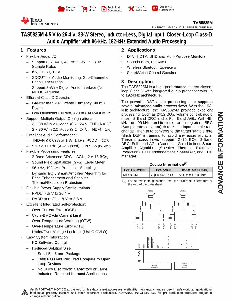
ADVANCE INFORMATION System Processor Digital Audio Source ADR PDN MUTE (GPIO1) FAULT (GPIO0) SDOUT (GPIO2) SDA SCL SDIN SCLK (BCLK) LRCLK BST_A+ OUT_A+ BST_A- OUT_A- BST_B+ OUT_B+ BST_B- OUT_B- Speaker L Channel Speaker R Channel Product Folder Order Now Technical Documents Tools & Software Support & Community An IMPORTANT NOTICE at the end of this data sheet addresses availability, warranty, changes, use in safety-critical applications, intellectual property matters and other important disclaimers. ADVANCE INFORMATION for pre-production products; subject to change without notice. TAS5825M SLASEH7A – MARCH 2018 – REVISED JUNE 2018 TAS5825M 4.5 V to 26.4 V, 38-W Stereo, Inductor-Less, Digital Input, Closed-Loop Class-D Audio Amplifier with 96-kHz, 192-kHz Extended Audio Processing 1 1 Features 1• Flexible Audio I/O: – Supports 32, 44.1, 48, 88.2, 96, 192 kHz Sample Rates – I 2 S, LJ, RJ, TDM – SDOUT for Audio Monitoring, Sub-Channel or Echo Cancellation – Support 3-Wire Digital Audio Interface (No MCLK Required) • Efficient Class-D Operation – Greater than 90% Power Efficiency, 90 mΩ R DS on – Low Quiescent Current, <20 mA at PVDD=12V • Support Multiple Output Configurations – 2 × 38 W in 2.0 Mode (6-Ω, 24 V, THD+N=1%) – 2 × 30 W in 2.0 Mode (8-Ω, 24 V, THD+N=1%) • Excellent Audio Performance: – THD+N ≤ 0.03% at 1 W, 1 kHz, PVDD = 12 V – SNR ≥ 110 dB (A-weighted), ICN ≤ 35 μVRMS • Flexible Processing Features – 3-Band Advanced DRC + AGL,2 × 15 BQs, – Sound Field Spatializer (SFS), Level Meter – 96-kHz, 192-kHz Processor Sampling – Dynamic EQ,Smart Amplifier Algorithm for Bass Enhancement and Speaker Thermal/Excursion Protection • Flexible Power Supply Configurations – PVDD: 4.5 V to 26.4 V – DVDD and I/O: 1.8 V or 3.3 V • Excellent Integrated self-protection: – Over-Current Error (OCE) – Cycle-By-Cycle Current Limit – Over-Temperature Warning (OTW) – Over-Temperature Error (OTE) – Under/Over-Voltage Lock-out (UVLO/OVLO) • Easy System Integration – I 2 C Software Control – Reduced Solution Size – Small 5 x 5 mm Package – Less Passives Required Compare to Open Loop Devices – No Bulky Electrolytic Capacitors or Large Inductors Required for most Applications 2 Applications • DTV, HDTV, UHD and Multi-Purpose Monitors • Sounds Bars, PC Audio • Wireless/Bluetooth Speakers • Smart/Voice Control Speakers 3 Description The TAS5825M is a high-performance, stereo closed- loop Class-D with integrated audio processor with up to 192-kHz architecture. The powerful DSP audio processing core supports several advanced audio process flows. With the 192- kHz architecture, the TAS5825M provides excellent processing. Such as 2×12 BQs, volume control, audio mixer, 2 Band DRC and a Full Band AGL. With 48- kHz or 96-kHz architecture, an integrated SRC (Sample rate convertor) detects the input sample rate change. Then auto converts to the target sample rate which DSP is running to avoid any audio artifacts. These process flows support: 2×15 BQs, 3-Band DRC, Full-band AGL (Automatic Gain Limiter), Smart Amplifier Algorithm (Speaker Thermal, Excursion Protection), Bass enhancement, Spatializer, and THD manager. Device Information (1) PART NUMBER PACKAGE BODY SIZE (NOM) TAS5825M VQFN (32) RHB 5.00 mm × 5.00 mm (1) For all available packages, see the orderable addendum at the end of the data sheet.
Transcript
AD
VA
NC
E I
NF
OR
MA
TIO
N
System Processor
DigitalAudioSource
AD
R
PD
N
MU
TE
(G
PIO
1)
FA
ULT
(G
PIO
0)
SD
OU
T (
GP
IO2
)
SD
A
SC
L
SD
IN
SC
LK (
BC
LK)
LRC
LK
BS
T_
A+
OU
T_
A+
BS
T_
A-
OU
T_
A-
BS
T_
B+
OU
T_
B+
BS
T_
B-
OU
T_
B-
SpeakerL Channel
SpeakerR Channel
Product
Folder
Order
Now
Technical
Documents
Tools &
Software
Support &Community
An IMPORTANT NOTICE at the end of this data sheet addresses availability, warranty, changes, use in safety-critical applications,intellectual property matters and other important disclaimers. ADVANCE INFORMATION for pre-production products; subject tochange without notice.
TAS5825MSLASEH7A –MARCH 2018–REVISED JUNE 2018
TAS5825M 4.5 V to 26.4 V, 38-W Stereo, Inductor-Less, Digital Input, Closed-Loop Class-DAudio Amplifier with 96-kHz, 192-kHz Extended Audio Processing
• Easy System Integration– I2C Software Control– Reduced Solution Size
– Small 5 x 5 mm Package– Less Passives Required Compare to Open
Loop Devices– No Bulky Electrolytic Capacitors or Large
Inductors Required for most Applications
2 Applications• DTV, HDTV, UHD and Multi-Purpose Monitors• Sounds Bars, PC Audio• Wireless/Bluetooth Speakers• Smart/Voice Control Speakers
3 DescriptionThe TAS5825M is a high-performance, stereo closed-loop Class-D with integrated audio processor with upto 192-kHz architecture.
The powerful DSP audio processing core supportsseveral advanced audio process flows. With the 192-kHz architecture, the TAS5825M provides excellentprocessing. Such as 2×12 BQs, volume control, audiomixer, 2 Band DRC and a Full Band AGL. With 48-kHz or 96-kHz architecture, an integrated SRC(Sample rate convertor) detects the input sample ratechange. Then auto converts to the target sample ratewhich DSP is running to avoid any audio artifacts.These process flows support: 2×15 BQs, 3-BandDRC, Full-band AGL (Automatic Gain Limiter), SmartAmplifier Algorithm (Speaker Thermal, ExcursionProtection), Bass enhancement, Spatializer, and THDmanager.
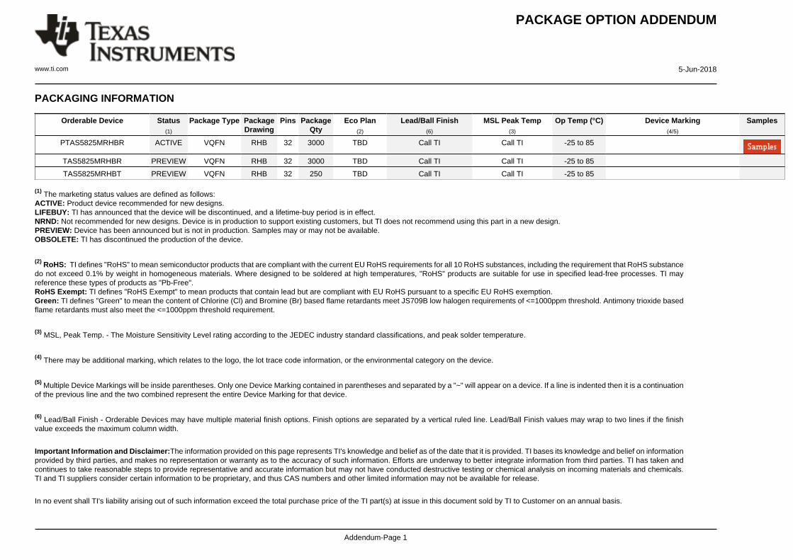
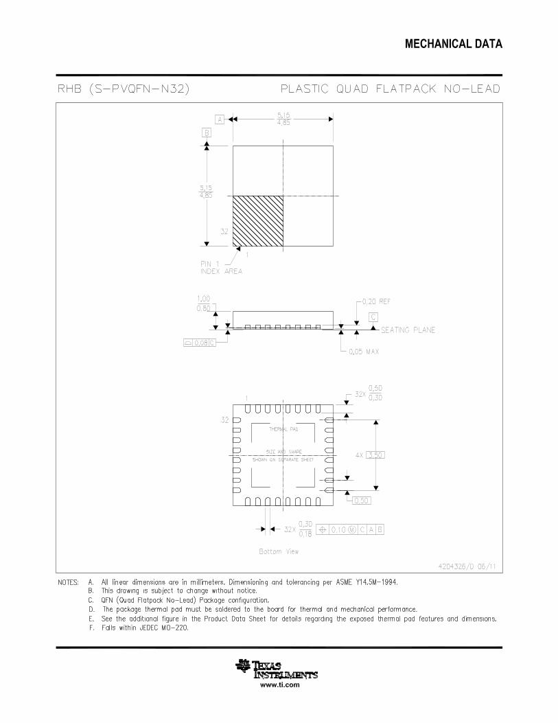
Device Information(1)
PART NUMBER PACKAGE BODY SIZE (NOM)TAS5825M VQFN (32) RHB 5.00 mm × 5.00 mm
(1) For all available packages, see the orderable addendum atthe end of the data sheet.
13 Device and Documentation Support ................. 8813.1 Device Support...................................................... 8813.2 Receiving Notification of Documentation Updates 8813.3 Community Resources.......................................... 8913.4 Trademarks ........................................................... 8913.5 Electrostatic Discharge Caution............................ 8913.6 Glossary ................................................................ 89
14 Mechanical, Packaging, and OrderableInformation ........................................................... 89
4 Revision HistoryNOTE: Page numbers for previous revisions may differ from page numbers in the current version.
DATE REVISION NOTESJanuary 2018 * Initial release.
March 2018 Version 1 Added the Spread Spectrum section.Removed Note for the description of Bit 1-0 in Table 8.
June 2018 A
Add the Typical Characteristics Graphs.Changed the Speaker Amplifier section of the ElectricalCharacteristics table.Updated the Application Schematic for both 2.0Mode/MONO Mode and 2.1 Mode.
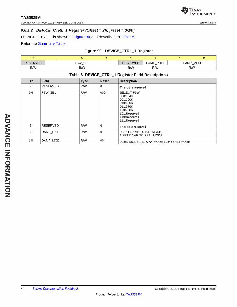
DEVICE NAME Modulation Scheme DSP Audio Process Flows
TAS5825MRHBHybrid Modulation/1SPW
Modulation (ExtendBattery Life Time)
Flexible Audio Process Flows
TAS5835MRHB BD Modulation Flexible Audio Process Flows
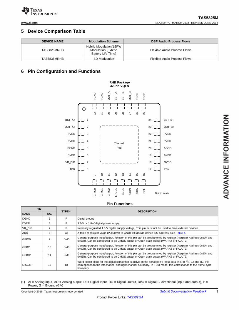
6 Pin Configuration and Functions
RHB Package32-Pin VQFN
(1) AI = Analog input, AO = Analog output, DI = Digital Input, DO = Digital Output, DI/O = Digital Bi-directional (input and output), P =Power, G = Ground (0 V)
Pin FunctionsPIN
TYPE (1) DESCRIPTIONNAME NO.
DGND 5 P Digital ground
DVDD 6 P 3.3-V or 1.8-V digital power supply
VR_DIG 7 P Internally regulated 1.5-V digital supply voltage. This pin must not be used to drive external devices
ADR 8 AI A table of resistor value (Pull down to GND) will decide device I2C address. See Table 4.
GPIO0 9 DI/O General-purpose input/output, function of this pin can be programmed by register (Register Address 0x60h and0x61h). Can be configured to be CMOS output or Open drain output (WARNZ or FAULTZ)
GPIO1 10 DI/O General-purpose input/output, function of this pin can be programmed by register (Register Address 0x60h and0x62h). Can be configured to be CMOS output or Open drain output (WARNZ or FAULTZ)
GPIO2 11 DI/O General-purpose input/output, function of this pin can be programmed by register (Register Address 0x60h and0x63h). Can be configured to be CMOS output or Open drain output (WARNZ or FAULTZ)
LRCLK 12 DIWord select clock for the digital signal that is active on the serial port's input data line. In I2S, LJ and RJ, thiscorresponds to the left channel and right channel boundary. In TDM mode, this corresponds to the frame syncboundary.
(2) Typically written "bit clock (BCLK)" in some audio codecs.
SCLK (2) 13 DI Bit clock for the digital signal that is active on the input data line of the serial data port. Sometimes, this pin also bewritten as "bit clock (BCLK)"
SDIN 14 DI Data line to the serial data port
SDA 15 DI/O I2C serial control data interface input/output
SCL 16 DI I2C serial control clock input
PDN 17 DI Power down, active-low. PDN place the amplifier in Shutdown, turn off all internal regulators.
GVDD 18 P Gate drive internal regulator output. This pin must not be used to drive external devices
AVDD 19 P Internally regulated 5-V analog supply voltage. This pin must not be used to drive external devices
AGND 20 P Analog ground
PVDD
3 P
PVDD voltage input4 P
21 P
22 P
PGND
25 P
Ground reference for power device circuitry. Connect this pin to system ground.26 P
31 P
32 P
OUT_B+ 23 O Positive pin for differential speaker amplifier output B
BST_B+ 24 P Connection point for the OUT_B+ bootstrap capacitor which is used to create a power supply for the high-sidegate drive for OUT_B+
OUT_B- 27 O Negative pin for differential speaker amplifier output B
BST_B- 28 P Connection point for the OUT_B- bootstrap capacitor which is used to create a power supply for the high-side gatedrive for OUT_B-
BST_A- 29 P Connection point for the OUT_A- bootstrap capacitor which is used to create a power supply for the high-side gatedrive for OUT_A-
OUT_A- 30 O Negative pin for differential speaker amplifier output A
BST_A+ 1 P Connection point for the OUT_A+ bootstrap capacitor which is used to create a power supply for the high-sidegate drive for OUT_A+
OUT_A+ 2 O Positive pin for differential speaker amplifier output A
(1) Stresses beyond those listed under Absolute Maximum Ratings may cause permanent damage to the device. Theseare stress ratingsonly, which do not imply functional operation of the device at these or anyother conditions beyond those indicated under RecommendedOperatingConditions. Exposure to absolute-maximum-rated conditions for extended periods mayaffect device reliability.
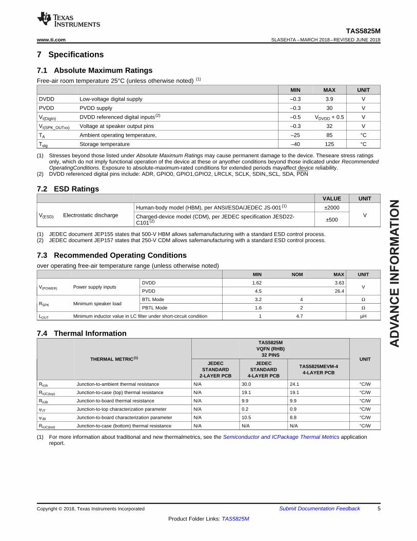
7.1 Absolute Maximum RatingsFree-air room temperature 25°C (unless otherwise noted) (1)
MIN MAX UNITDVDD Low-voltage digital supply –0.3 3.9 VPVDD PVDD supply –0.3 30 VVI(DigIn) DVDD referenced digital inputs (2) –0.5 VDVDD + 0.5 VVI(SPK_OUTxx) Voltage at speaker output pins –0.3 32 VTA Ambient operating temperature, –25 85 °CTstg Storage temperature –40 125 °C
(1) JEDEC document JEP155 states that 500-V HBM allows safemanufacturing with a standard ESD control process.(2) JEDEC document JEP157 states that 250-V CDM allows safemanufacturing with a standard ESD control process.
7.2 ESD RatingsVALUE UNIT
V(ESD) Electrostatic dischargeHuman-body model (HBM), per ANSI/ESDA/JEDEC JS-001 (1) ±2000
VCharged-device model (CDM), per JEDEC specification JESD22-C101 (2) ±500
7.3 Recommended Operating Conditionsover operating free-air temperature range (unless otherwise noted)
MIN NOM MAX UNIT
V(POWER) Power supply inputsDVDD 1.62 3.63
VPVDD 4.5 26.4
RSPK Minimum speaker loadBTL Mode 3.2 4 Ω
PBTL Mode 1.6 2 Ω
LOUT Minimum inductor value in LC filter under short-circuit condition 1 4.7 µH
(1) For more information about traditional and new thermalmetrics, see the Semiconductor and ICPackage Thermal Metrics applicationreport.
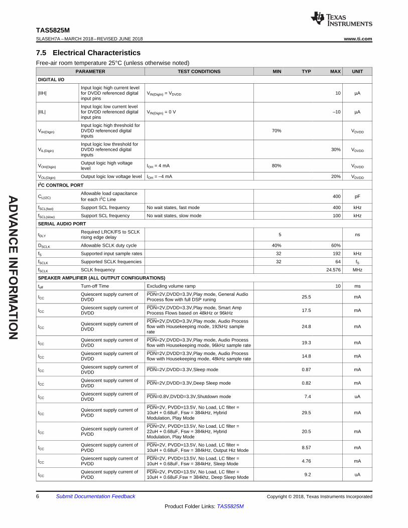
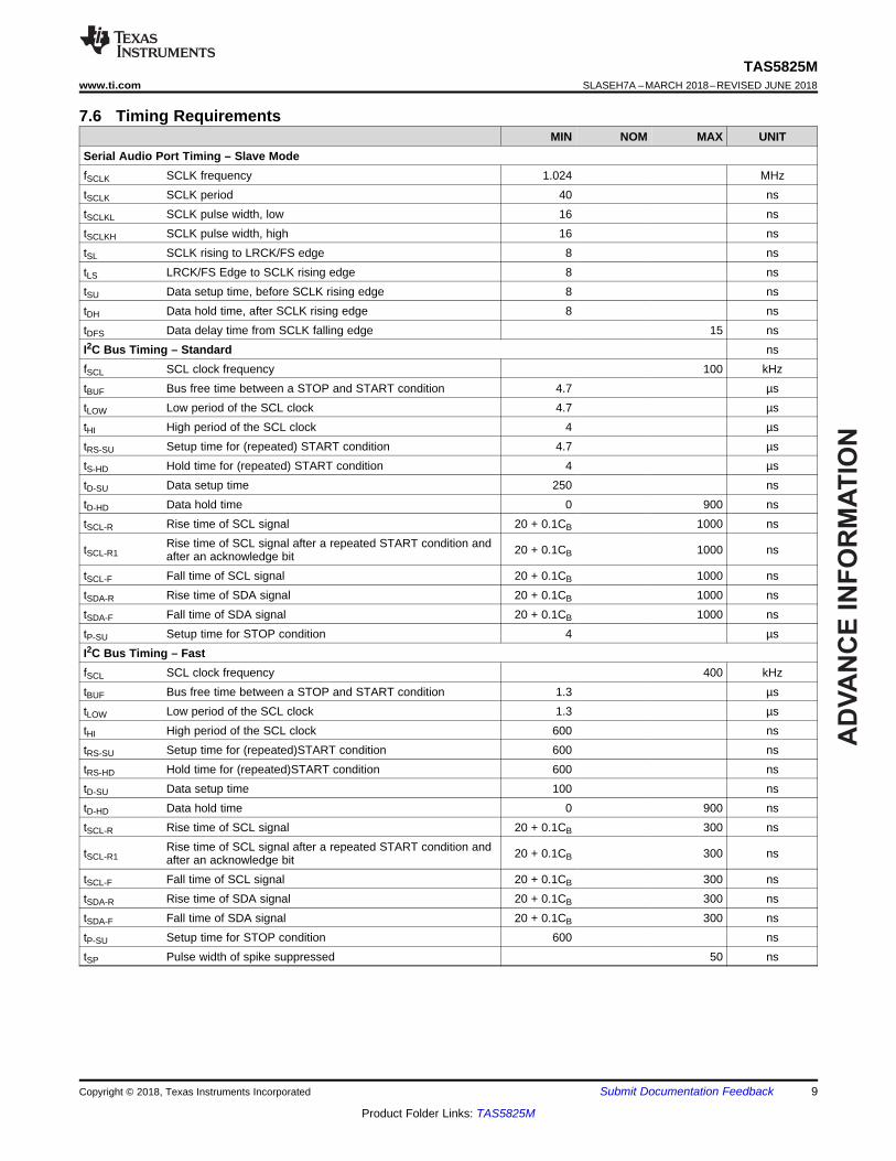
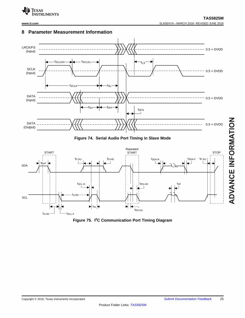
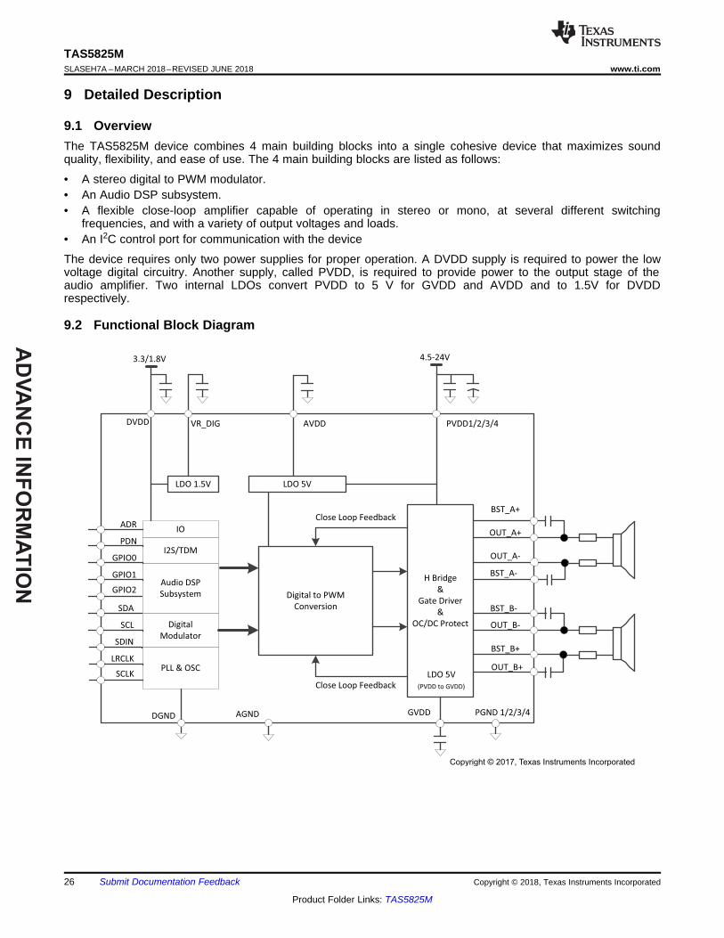
Serial Audio Port Timing – Slave ModefSCLK SCLK frequency 1.024 MHztSCLK SCLK period 40 nstSCLKL SCLK pulse width, low 16 nstSCLKH SCLK pulse width, high 16 nstSL SCLK rising to LRCK/FS edge 8 nstLS LRCK/FS Edge to SCLK rising edge 8 nstSU Data setup time, before SCLK rising edge 8 nstDH Data hold time, after SCLK rising edge 8 nstDFS Data delay time from SCLK falling edge 15 nsI2C Bus Timing – Standard nsfSCL SCL clock frequency 100 kHztBUF Bus free time between a STOP and START condition 4.7 µstLOW Low period of the SCL clock 4.7 µstHI High period of the SCL clock 4 µstRS-SU Setup time for (repeated) START condition 4.7 µstS-HD Hold time for (repeated) START condition 4 µstD-SU Data setup time 250 nstD-HD Data hold time 0 900 nstSCL-R Rise time of SCL signal 20 + 0.1CB 1000 ns
tSCL-R1Rise time of SCL signal after a repeated START condition andafter an acknowledge bit 20 + 0.1CB 1000 ns
tSCL-F Fall time of SCL signal 20 + 0.1CB 1000 nstSDA-R Rise time of SDA signal 20 + 0.1CB 1000 nstSDA-F Fall time of SDA signal 20 + 0.1CB 1000 nstP-SU Setup time for STOP condition 4 µsI2C Bus Timing – FastfSCL SCL clock frequency 400 kHztBUF Bus free time between a STOP and START condition 1.3 µstLOW Low period of the SCL clock 1.3 µstHI High period of the SCL clock 600 nstRS-SU Setup time for (repeated)START condition 600 nstRS-HD Hold time for (repeated)START condition 600 nstD-SU Data setup time 100 nstD-HD Data hold time 0 900 nstSCL-R Rise time of SCL signal 20 + 0.1CB 300 ns
tSCL-R1Rise time of SCL signal after a repeated START condition andafter an acknowledge bit 20 + 0.1CB 300 ns
tSCL-F Fall time of SCL signal 20 + 0.1CB 300 nstSDA-R Rise time of SDA signal 20 + 0.1CB 300 nstSDA-F Fall time of SDA signal 20 + 0.1CB 300 nstP-SU Setup time for STOP condition 600 nstSP Pulse width of spike suppressed 50 ns
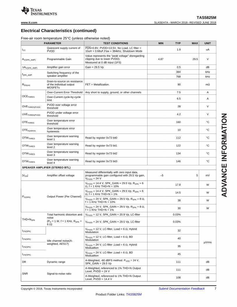
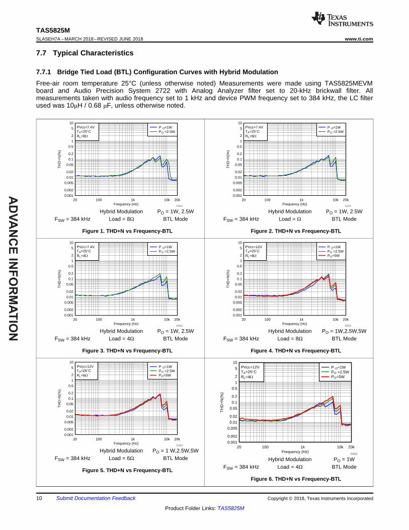
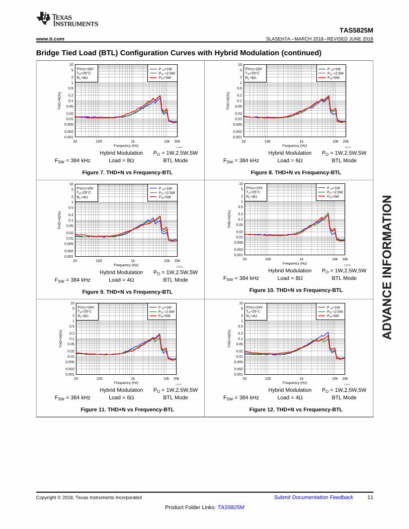
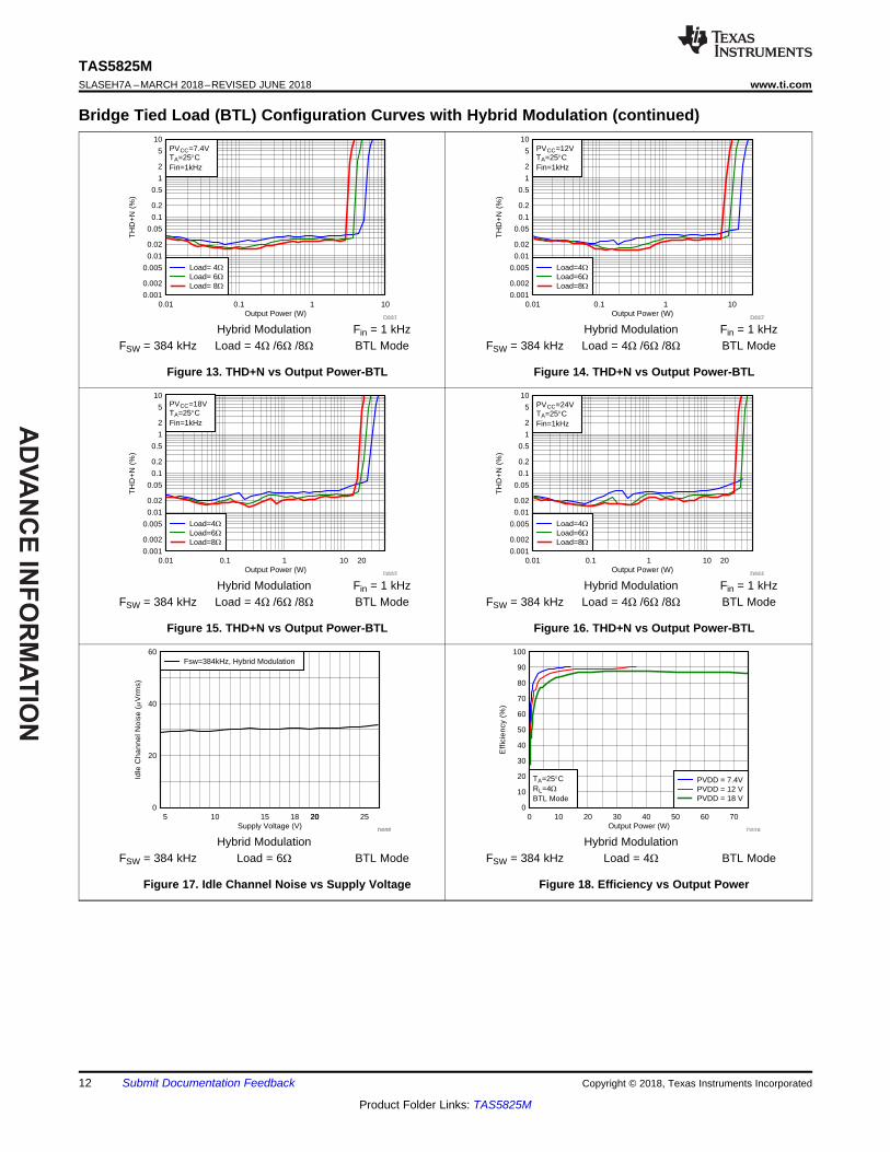
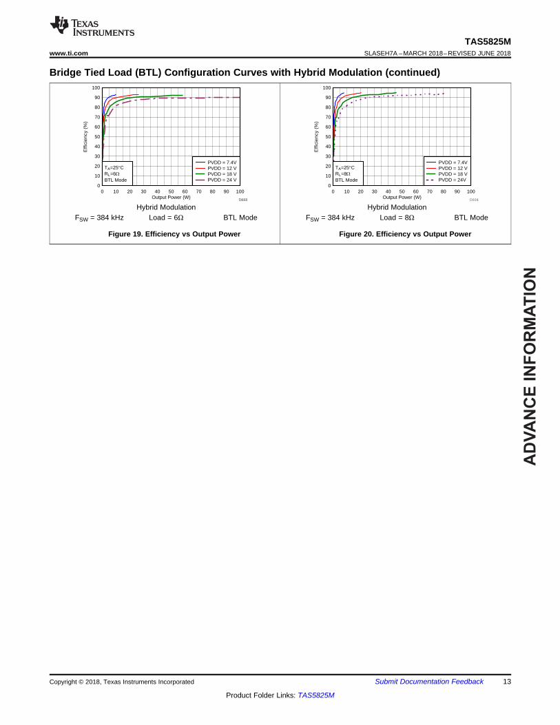
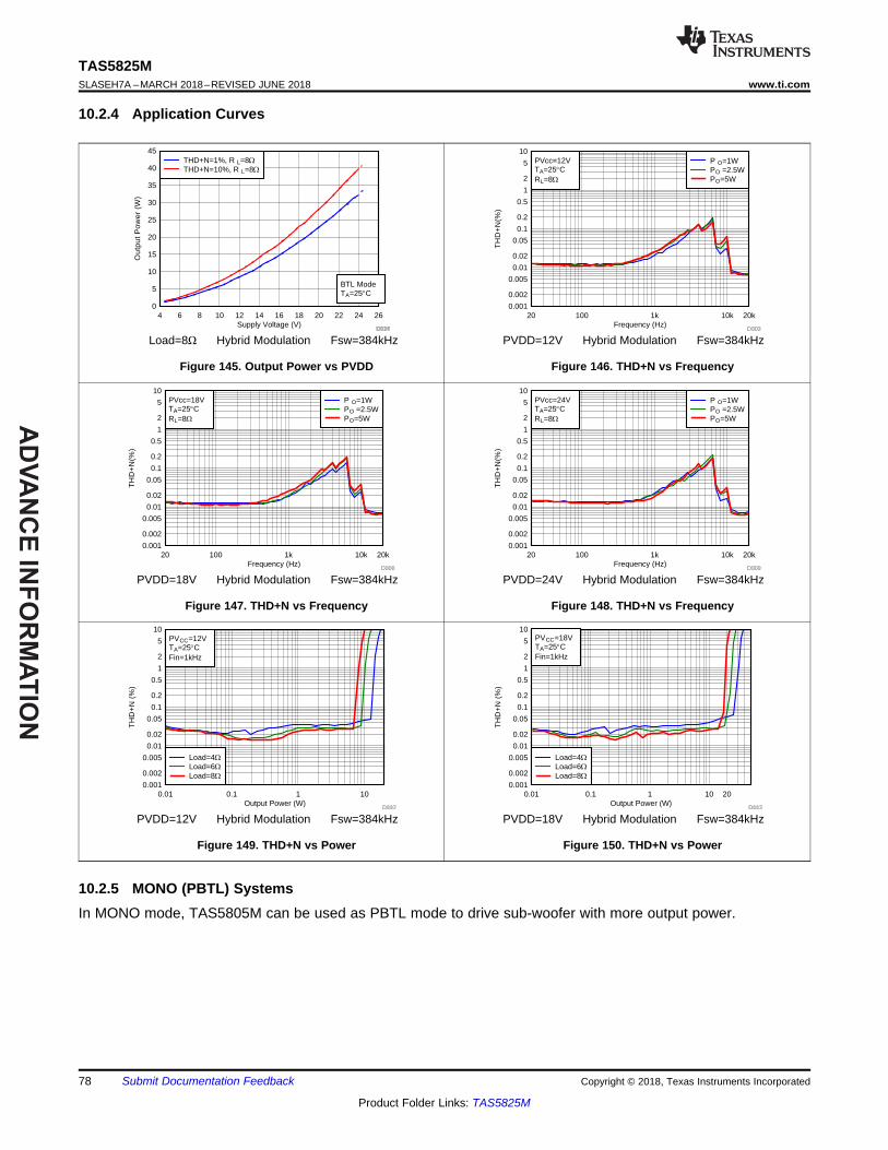
7.7.1 Bridge Tied Load (BTL) Configuration Curves with Hybrid ModulationFree-air room temperature 25°C (unless otherwise noted) Measurements were made using TAS5825MEVMboard and Audio Precision System 2722 with Analog Analyzer filter set to 20-kHz brickwall filter. Allmeasurements taken with audio frequency set to 1 kHz and device PWM frequency set to 384 kHz, the LC filterused was 10μH / 0.68 μF, unless otherwise noted.
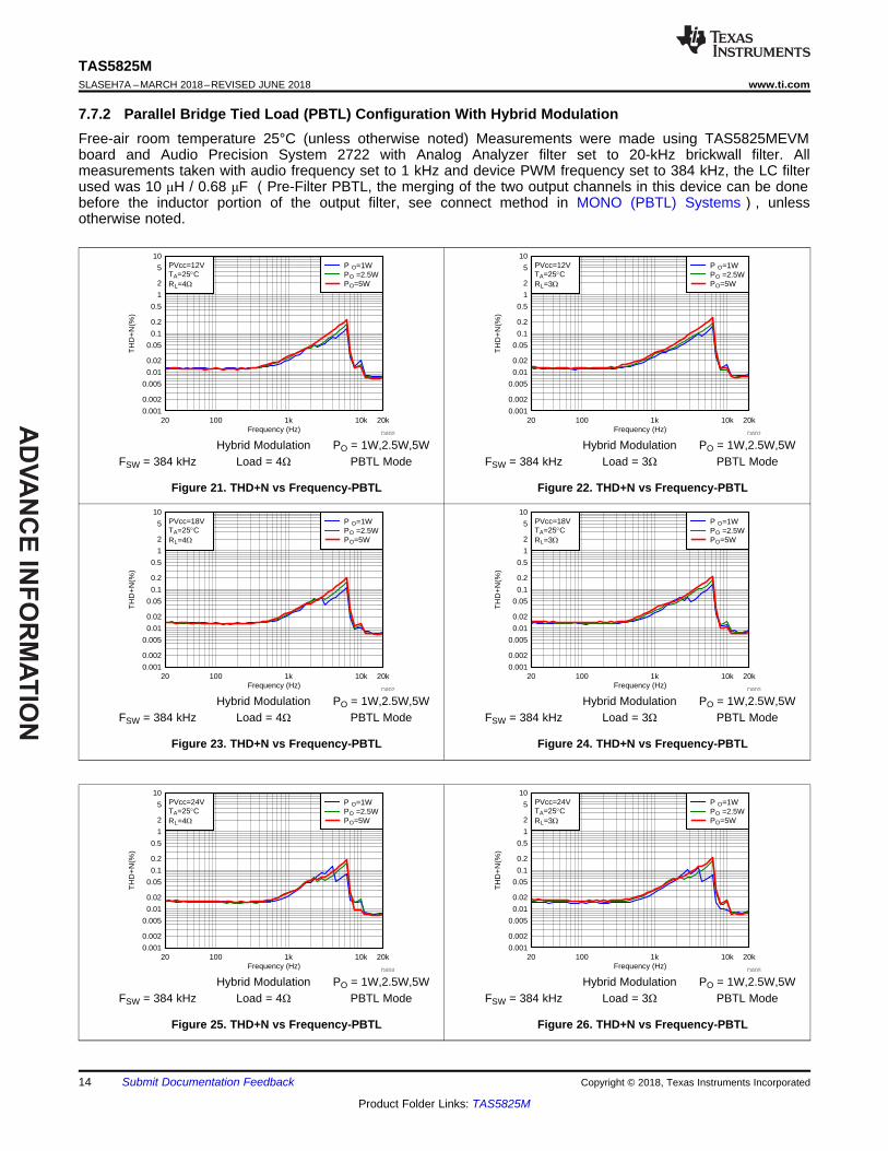
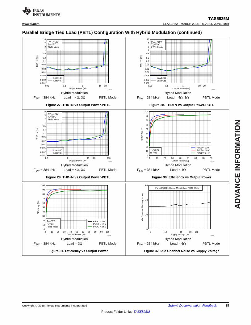
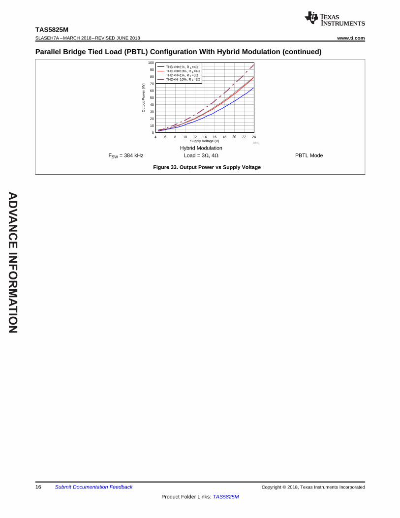
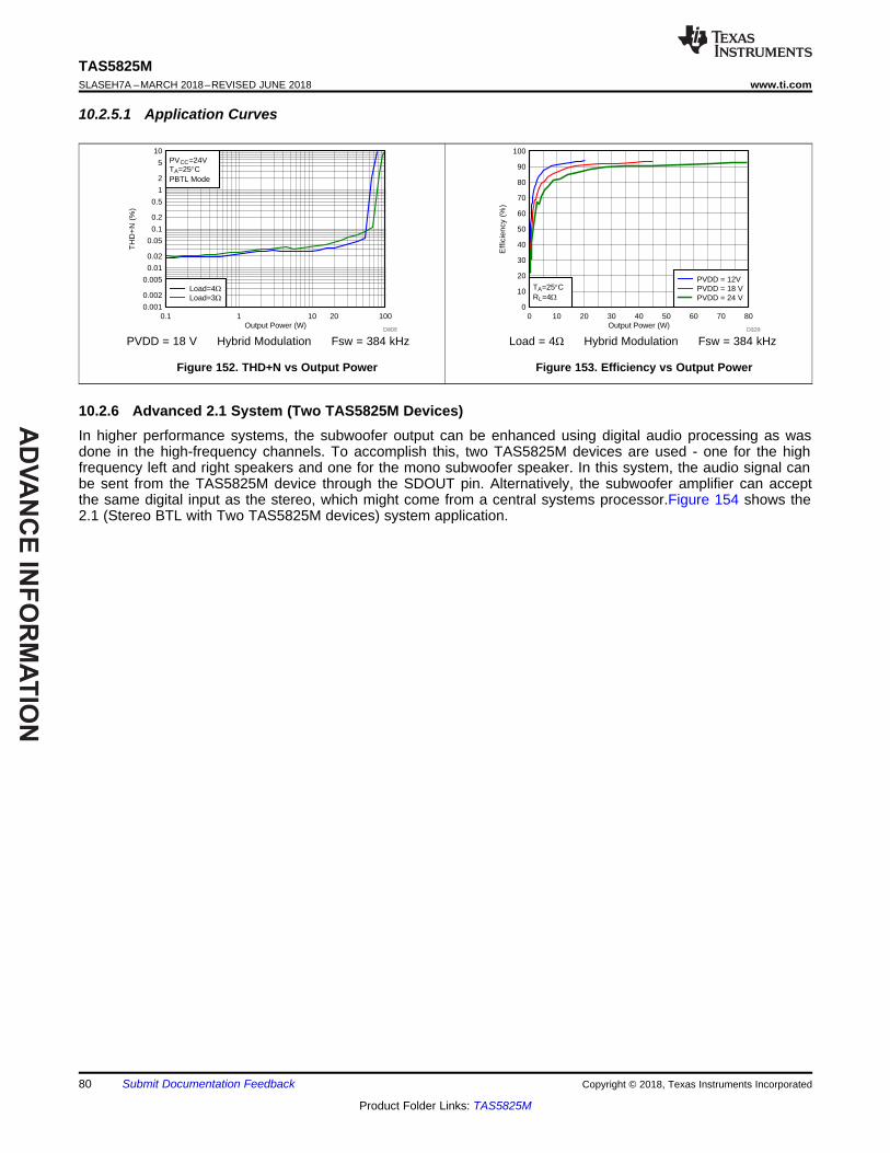
7.7.2 Parallel Bridge Tied Load (PBTL) Configuration With Hybrid ModulationFree-air room temperature 25°C (unless otherwise noted) Measurements were made using TAS5825MEVMboard and Audio Precision System 2722 with Analog Analyzer filter set to 20-kHz brickwall filter. Allmeasurements taken with audio frequency set to 1 kHz and device PWM frequency set to 384 kHz, the LC filterused was 10 μH / 0.68 μF (Pre-Filter PBTL, the merging of the two output channels in this device can be donebefore the inductor portion of the output filter, see connect method in MONO (PBTL) Systems), unlessotherwise noted.
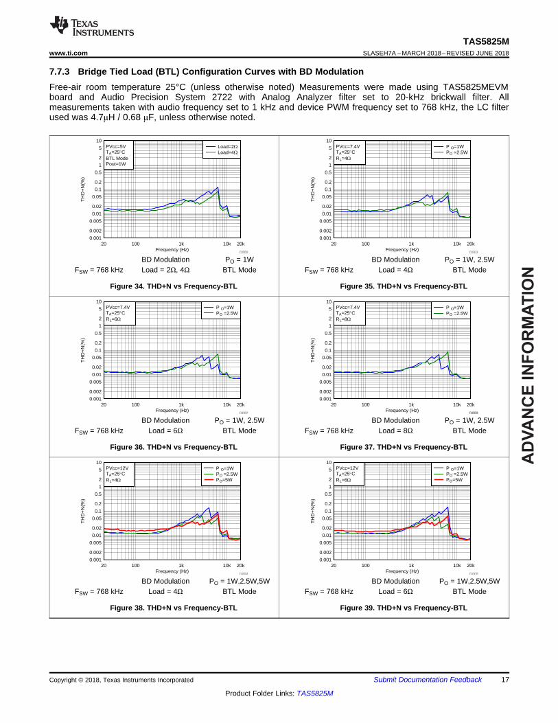
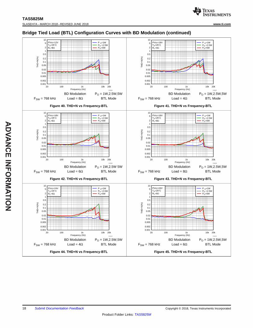
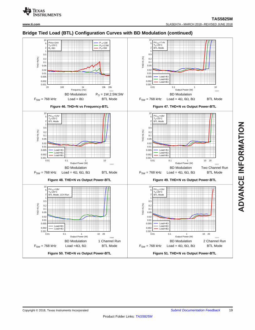
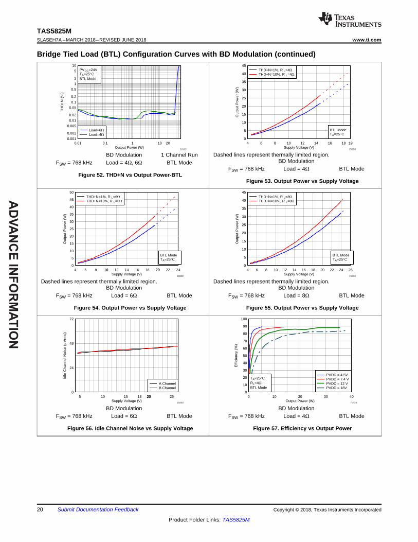
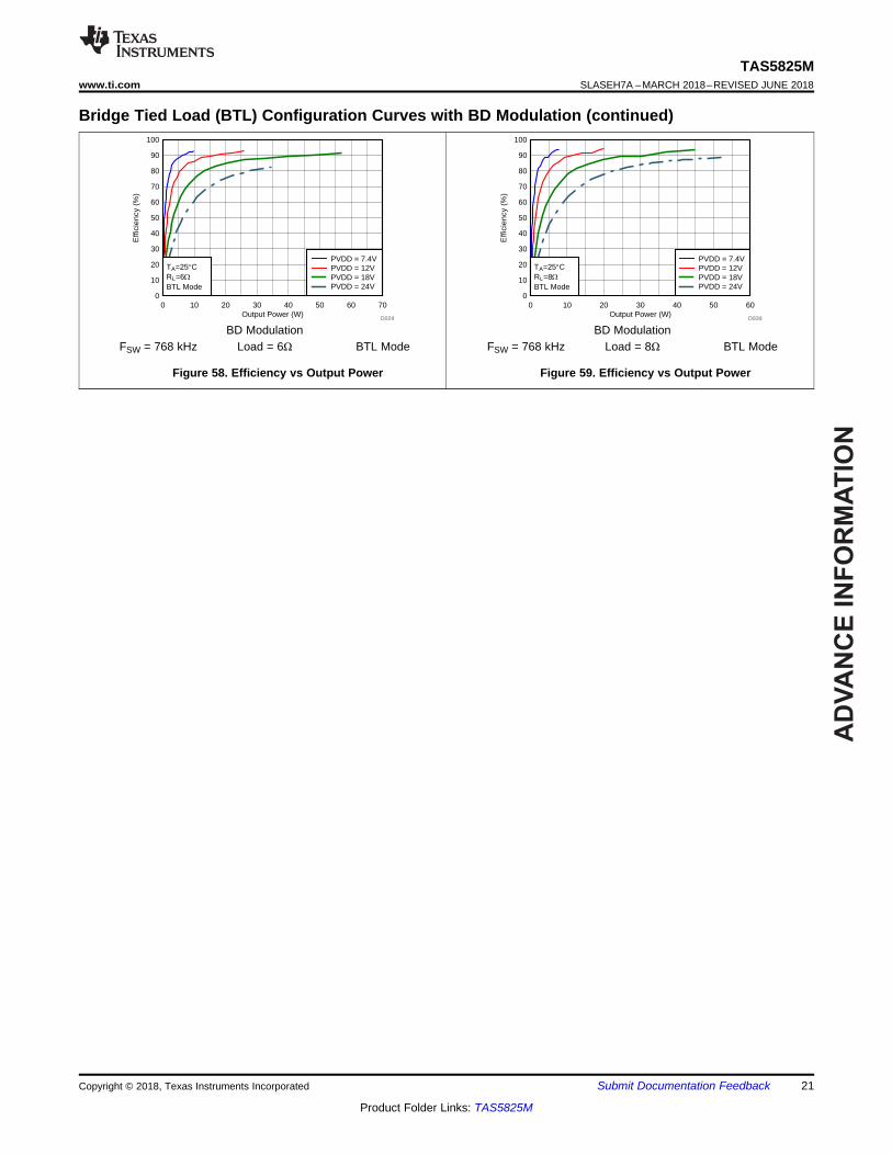
7.7.3 Bridge Tied Load (BTL) Configuration Curves with BD ModulationFree-air room temperature 25°C (unless otherwise noted) Measurements were made using TAS5825MEVMboard and Audio Precision System 2722 with Analog Analyzer filter set to 20-kHz brickwall filter. Allmeasurements taken with audio frequency set to 1 kHz and device PWM frequency set to 768 kHz, the LC filterused was 4.7μH / 0.68 μF, unless otherwise noted.
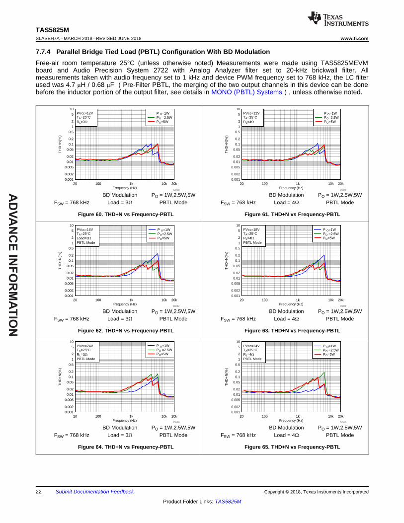
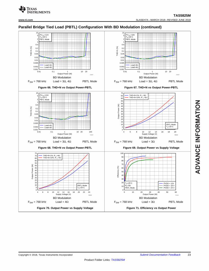
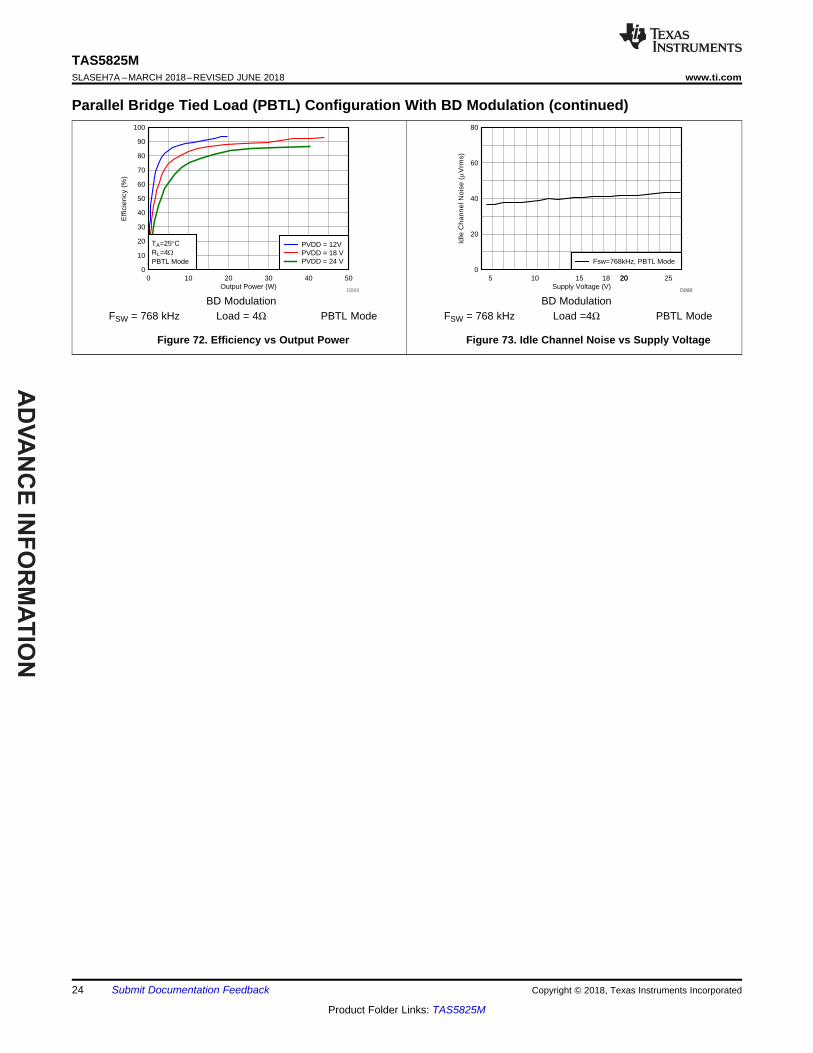
7.7.4 Parallel Bridge Tied Load (PBTL) Configuration With BD ModulationFree-air room temperature 25°C (unless otherwise noted) Measurements were made using TAS5825MEVMboard and Audio Precision System 2722 with Analog Analyzer filter set to 20-kHz brickwall filter. Allmeasurements taken with audio frequency set to 1 kHz and device PWM frequency set to 768 kHz, the LC filterused was 4.7 μH / 0.68 μF (Pre-Filter PBTL, the merging of the two output channels in this device can be donebefore the inductor portion of the output filter, see details in MONO (PBTL) Systems), unless otherwise noted.
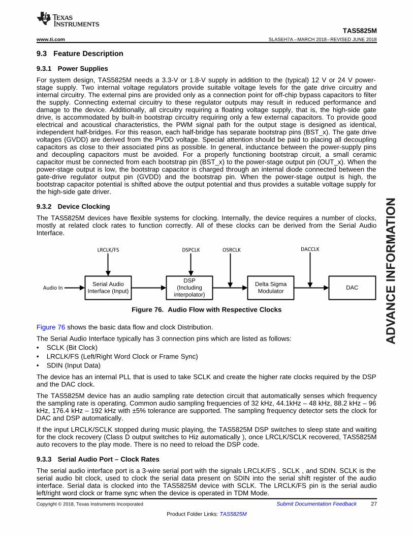
9.1 OverviewThe TAS5825M device combines 4 main building blocks into a single cohesive device that maximizes soundquality, flexibility, and ease of use. The 4 main building blocks are listed as follows:
• A stereo digital to PWM modulator.• An Audio DSP subsystem.• A flexible close-loop amplifier capable of operating in stereo or mono, at several different switching
frequencies, and with a variety of output voltages and loads.• An I2C control port for communication with the device
The device requires only two power supplies for proper operation. A DVDD supply is required to power the lowvoltage digital circuitry. Another supply, called PVDD, is required to provide power to the output stage of theaudio amplifier. Two internal LDOs convert PVDD to 5 V for GVDD and AVDD and to 1.5V for DVDDrespectively.
9.3.1 Power SuppliesFor system design, TAS5825M needs a 3.3-V or 1.8-V supply in addition to the (typical) 12 V or 24 V power-stage supply. Two internal voltage regulators provide suitable voltage levels for the gate drive circuitry andinternal circuitry. The external pins are provided only as a connection point for off-chip bypass capacitors to filterthe supply. Connecting external circuitry to these regulator outputs may result in reduced performance anddamage to the device. Additionally, all circuitry requiring a floating voltage supply, that is, the high-side gatedrive, is accommodated by built-in bootstrap circuitry requiring only a few external capacitors. To provide goodelectrical and acoustical characteristics, the PWM signal path for the output stage is designed as identical,independent half-bridges. For this reason, each half-bridge has separate bootstrap pins (BST_x). The gate drivevoltages (GVDD) are derived from the PVDD voltage. Special attention should be paid to placing all decouplingcapacitors as close to their associated pins as possible. In general, inductance between the power-supply pinsand decoupling capacitors must be avoided. For a properly functioning bootstrap circuit, a small ceramiccapacitor must be connected from each bootstrap pin (BST_x) to the power-stage output pin (OUT_x). When thepower-stage output is low, the bootstrap capacitor is charged through an internal diode connected between thegate-drive regulator output pin (GVDD) and the bootstrap pin. When the power-stage output is high, thebootstrap capacitor potential is shifted above the output potential and thus provides a suitable voltage supply forthe high-side gate driver.
9.3.2 Device ClockingThe TAS5825M devices have flexible systems for clocking. Internally, the device requires a number of clocks,mostly at related clock rates to function correctly. All of these clocks can be derived from the Serial AudioInterface.
Figure 76. Audio Flow with Respective Clocks
Figure 76 shows the basic data flow and clock Distribution.
The Serial Audio Interface typically has 3 connection pins which are listed as follows:• SCLK (Bit Clock)• LRCLK/FS (Left/Right Word Clock or Frame Sync)• SDIN (Input Data)
The device has an internal PLL that is used to take SCLK and create the higher rate clocks required by the DSPand the DAC clock.
The TAS5825M device has an audio sampling rate detection circuit that automatically senses which frequencythe sampling rate is operating. Common audio sampling frequencies of 32 kHz, 44.1kHz – 48 kHz, 88.2 kHz – 96kHz, 176.4 kHz – 192 kHz with ±5% tolerance are supported. The sampling frequency detector sets the clock forDAC and DSP automatically.
If the input LRCLK/SCLK stopped during music playing, the TAS5825M DSP switches to sleep state and waitingfor the clock recovery (Class D output switches to Hiz automatically ), once LRCLK/SCLK recovered, TAS5825Mauto recovers to the play mode. There is no need to reload the DSP code.
9.3.3 Serial Audio Port – Clock RatesThe serial audio interface port is a 3-wire serial port with the signals LRCLK/FS , SCLK , and SDIN. SCLK is theserial audio bit clock, used to clock the serial data present on SDIN into the serial shift register of the audiointerface. Serial data is clocked into the TAS5825M device with SCLK. The LRCLK/FS pin is the serial audioleft/right word clock or frame sync when the device is operated in TDM Mode.
Feature Description (continued)Table 1. Audio Data Formats, Bit Depths and Clock Rates
FORMAT DATA BITS MAXIMUM LRCLK/FS FREQUENCY(kHz) SCLK RATE (fS)
I2S/LJ/RJ 32, 24, 20, 16 Up to 192 64, 32
TDM 32, 24, 20, 16Up to 48 128,256,512
96 128,256192 128
When any kind of clock error, Out of Range, SCLK-FSYNC Ratio, or Clock halt is detected, the device puts allchannels into the Hi-Z state and report Clock Error in Register 113 (Register Address 0x71). When all audioclocks are within the expected ranges, the device automatically returns to the state it was in, but the clock errorflag in register 113 need to cleared by Register 120 (Register Address 0x78) manually .
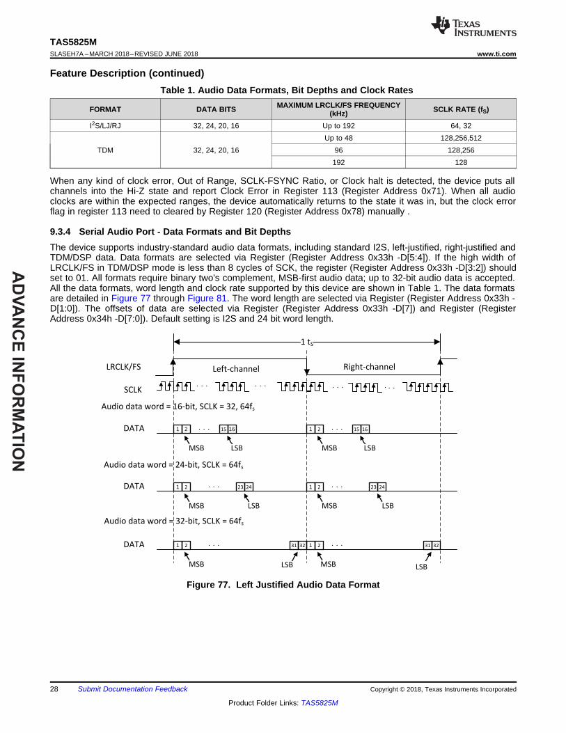
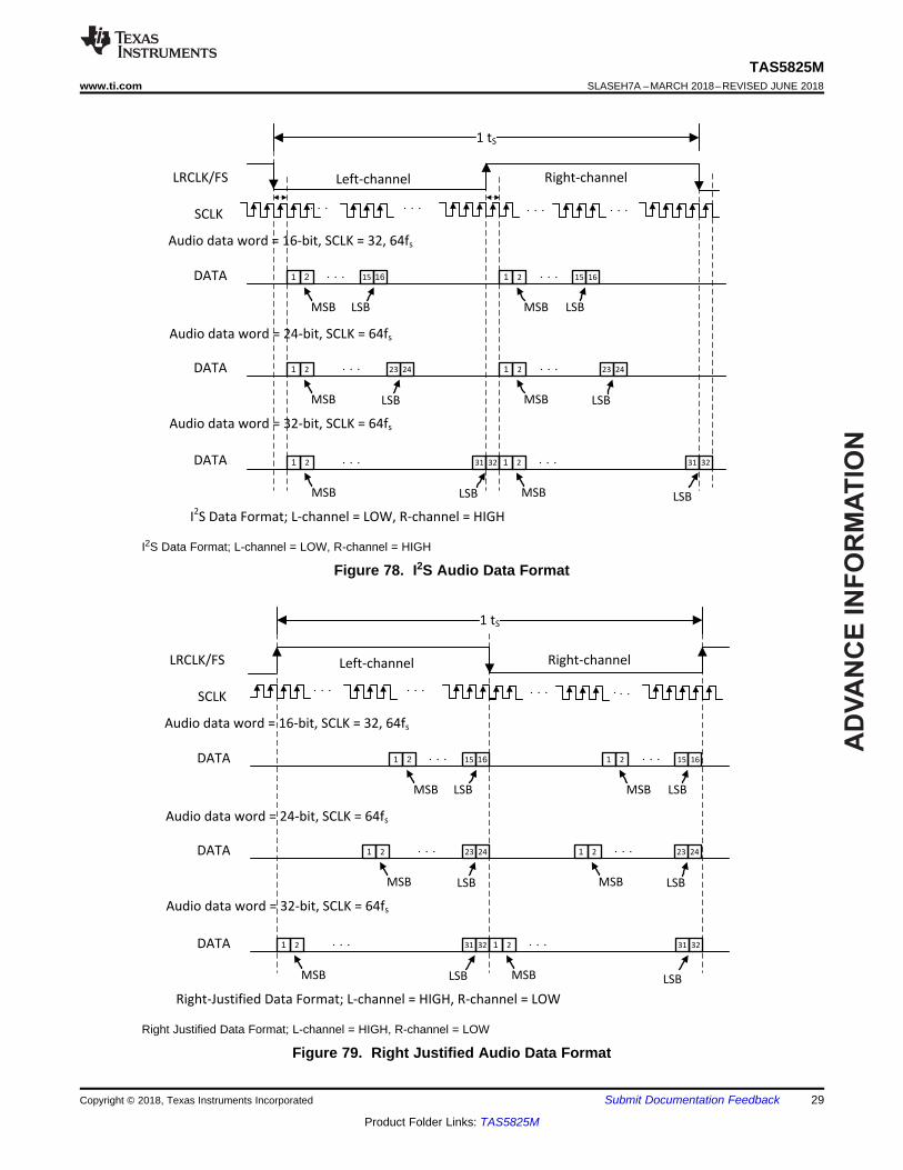
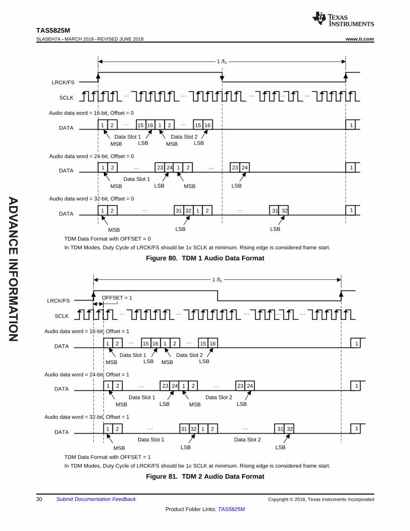
9.3.4 Serial Audio Port - Data Formats and Bit DepthsThe device supports industry-standard audio data formats, including standard I2S, left-justified, right-justified andTDM/DSP data. Data formats are selected via Register (Register Address 0x33h -D[5:4]). If the high width ofLRCLK/FS in TDM/DSP mode is less than 8 cycles of SCK, the register (Register Address 0x33h -D[3:2]) shouldset to 01. All formats require binary two's complement, MSB-first audio data; up to 32-bit audio data is accepted.All the data formats, word length and clock rate supported by this device are shown in Table 1. The data formatsare detailed in Figure 77 through Figure 81. The word length are selected via Register (Register Address 0x33h -D[1:0]). The offsets of data are selected via Register (Register Address 0x33h -D[7]) and Register (RegisterAddress 0x34h -D[7:0]). Default setting is I2S and 24 bit word length.
9.3.5 Digital Audio ProcessingTAS5825M DSP has flexible process flows for different applications, refer to application note, TAS5825MProcess Flows for details.
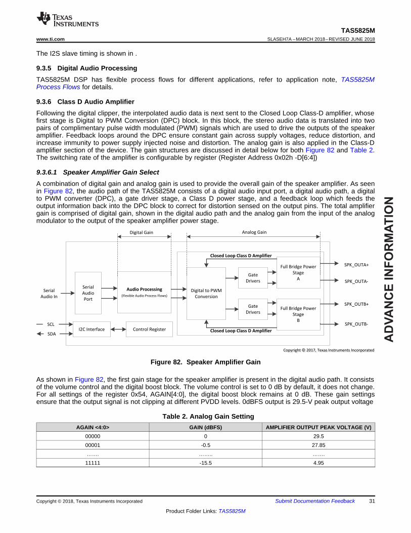
9.3.6 Class D Audio AmplifierFollowing the digital clipper, the interpolated audio data is next sent to the Closed Loop Class-D amplifier, whosefirst stage is Digital to PWM Conversion (DPC) block. In this block, the stereo audio data is translated into twopairs of complimentary pulse width modulated (PWM) signals which are used to drive the outputs of the speakeramplifier. Feedback loops around the DPC ensure constant gain across supply voltages, reduce distortion, andincrease immunity to power supply injected noise and distortion. The analog gain is also applied in the Class-Damplifier section of the device. The gain structures are discussed in detail below for both Figure 82 and Table 2.The switching rate of the amplifier is configurable by register (Register Address 0x02h -D[6:4])
9.3.6.1 Speaker Amplifier Gain SelectA combination of digital gain and analog gain is used to provide the overall gain of the speaker amplifier. As seenin Figure 82, the audio path of the TAS5825M consists of a digital audio input port, a digital audio path, a digitalto PWM converter (DPC), a gate driver stage, a Class D power stage, and a feedback loop which feeds theoutput information back into the DPC block to correct for distortion sensed on the output pins. The total amplifiergain is comprised of digital gain, shown in the digital audio path and the analog gain from the input of the analogmodulator to the output of the speaker amplifier power stage.
Figure 82. Speaker Amplifier Gain
As shown in Figure 82, the first gain stage for the speaker amplifier is present in the digital audio path. It consistsof the volume control and the digital boost block. The volume control is set to 0 dB by default, it does not change.For all settings of the register 0x54, AGAIN[4:0], the digital boost block remains at 0 dB. These gain settingsensure that the output signal is not clipping at different PVDD levels. 0dBFS output is 29.5-V peak output voltage
Table 2. Analog Gain SettingAGAIN <4:0> GAIN (dBFS) AMPLIFIER OUTPUT PEAK VOLTAGE (V)
9.4.1 Software ControlThe TAS5825M device is configured via an I2 C communication port.
The I2C Communication Protocol is detailed in the I2C Communication Port section. The I2C timing requirementsare described in the I2C Bus Timing – Standard and I2C Bus Timing – Fast sections.
There are two methods to program TAS5825M DSP memory.• Loading with I2C Communication Port by host processor. This method is recommend for most of applications.• Fast loading from external EEPROM with SPI communication Port. This method can be used in some
applications which need fast loading to save initialization time or release the Host Controller's loading.TAS525M supports to load the DSP memory data from external EEPROM via SPI. The GPIOs can beconfigured as SI,SO and SCK for EEPROM via Register (0x60,0x61,0x62,0x63,0x64). The chip selection CSof EEPROM is controlled by the Host Processor. See AppNote: DSP Code Fast Loading From ExternalEEPROM via SPI.
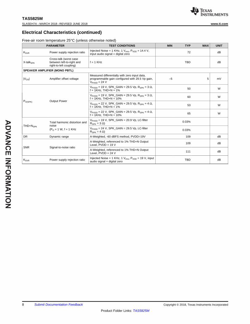
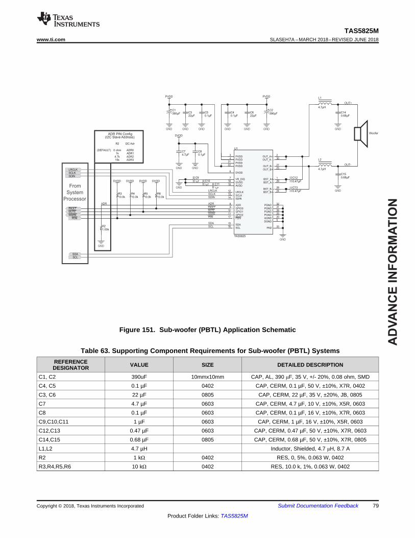
9.4.2 Speaker Amplifier Operating ModesThe TAS5825M device can be used with two different amplifier configurations, can be configured by Register0x02h -D[2]:• BTL Mode• PBTL Mode
9.4.2.1 BTL ModeIn BTL mode, the TAS5825M amplifies two independent signals, which represent the left and right portions of astereo signal. The amplified left signal is presented on differential output pair shown as OUT_A+ and OUT_A-,the amplified right signal is presented on differential output pair shown as OUT_B+ and OUT_B-.
9.4.2.2 PBTL ModeThe PBTL mode of operation is used to describe operation in which the two outputs of the device are placed inparallel with one another to increase the power sourcing capabilities of the device. On the output side of theTAS5825M device, the summation of the devices can be done before the filter in a configuration called Pre-FilterParallel Bridge Tied Load (PBTL). However, the two outputs can be required to merge together after the inductorportion of the output filter. Doing so does require two additional inductors, but allows smaller, less expensiveinductors to be used because the current is divided between the two inductors. The process is called Post-FilterPBTL. On the input side of the TAS5825M device, the input signal to the PBTL amplifier is left frame of I2S orTDM data.
9.4.3 Low EMI ModesTAS5825M employs several modes to minimize EMI during playing audio, and they can be used based ondifferent applications.
9.4.3.1 Spread SpectrumSpread spectrum is used in some inductor free case to minimize EMI noise. The TAS5825M supports SpreadSpectrum with triangle mode.
User need configure register SS_CTRL0 (0x6B) to Enable triangle mode and enable spread spectrum, selectspread spectrum frequency and range with SS_CTRL1 (0x6C). For 384kHz FSW which configured byDEVICE_CTRL1 (0x02), the spread spectrum frequency and range are described in Table 3.
Table 3. Triangle Mode Spread Spectrum Frequency and Range SelectionSS_TRI_CTRL
Device Functional Modes (continued)Table 3. Triangle Mode Spread Spectrum Frequency and Range Selection (continued)
SS_TRI_CTRL[3:0] 0 1 2 3 4 5 6 7
SpreadSpectrum
Range5% 10% 20% 25% 5% 10% 20% 25%
User Application example: Central Switching Frequency is 384kHz, Triangle Frequency is 24kHz.
Register 0x6b = 0x03 // Enable Spread Spectrum
Register 0x6c = 0x03 // SS_CTRL[3:0]=0011, Triangle Frequency = 24kHz, Spread Spectrum Range should be25% (336kHz~432kHz)
9.4.3.2 Channel to Channel Phase ShiftThis device supports channel to channel 180-degree PWM phase shift to minimize the EMI. Bit 0 of Register0x53 can be used to disable or enable the phase shift.
9.4.3.3 Multi-Devices PWM Phase SynchronizationTAS5825M support up to 4 phases selection for the multi devices application system. For example, when asystem integrated 4 TAS5825M devices, user can select phase0/1/2/3 for each device by registerPHASE_CTRL(0x6A), which means there is a 45 degree phase shift between each device to minimize the EMI.
There are two methods for Multi-Device PWM phase synchronization. Phase Synchronization With I2S Clock InStartup Phase or Phase Synchronization With GPIO.
9.4.3.3.1 Phase Synchronization With I2S Clock In Startup Phase1. Step 1, Halt I2S clock.2. Step 2, Configure each device phase selection and enable the phase synchronization. For example: Register
0x6A=0x03 for device 0; Register 0x6A=0x07 for device 1; Register 0x6A=0x0B for device 2; Register0x6A=0x0F for device 3.
3. Step 3, Configure each device into HIZ mode.4. Step 4, Provide I2S to each device. Phase synchronization for all 4 devices will be automatically done by
internal sequence.5. Step 5, Initialize the DSP code (This step can be skipped if only need to do the Phase Synchronization).6. Step 6, Device to Device PWM phase shift should be fixed with 45 degree.
9.4.3.3.2 Phase Synchronization With GPIO1. Step 1, Connect GPIOx pin of each device to SOC's GPIO pin on PCB.2. Step 2, Configure each device GPIOx as phase sync input usage by registers GPIO_CTRL (0X60) and
GPIO_INPUT_SEL (0x64).3. Step 3, Select different phase for each device and enable phase synchronization by register PHASE_CTRL
(0x6A).4. Step 4, Configure each device into PLAY mode by register DEVICE_CTRL2 (0x03) and monitor the
POWER_STATE register (0x68) until device changed to HIZ state.5. Step 5, Give a 0 to 1 toggle on SOC GPIO. Then all 4 devices will enter into PLAY mode and device to
Device PWM phase shift should be fixed with 45 degree.6. Step 6, Phase Synchronization has been finished. Configure the GPIOx pin to other function based on the
application.
9.4.4 Device State ControlExcept Shutdown Mode, TAS5825M has other 4 states for different power dissipation which listed in theElectrical Characteristics Table.• Deep Sleep Mode. Register 0x03h -D[1:0]=00, Device stays in Deep Sleep Mode. In this mode, I2 C block
keep works. This mode can be used to extend the battery life time in some portable speaker application case,once the host processor stopped playing audio for a long time, TAS5825M can be set to Deep Sleep Mode tominimize power dissipation until host processor start playing audio again. Device returns back to Play Modeby setting Register 0x03h -D[1:0] to 11. Compare with Shutdown Mode (Pull PDN Low), enter or exit DeepSleep Mode, DSP keeps active.
• Sleep Mode. Register 0x03h -D[1:0]=01, Device stays in Sleep Mode. In this mode, I2 C block, Digital core,DSP Memory , 5V Analog LDO keep works. Compare with Shutdown Mode (Pull PDN Low), enter or exitSleep Mode, DSP keeps active.
• Output Hiz Mode. Register 0x03h -D[1:0]=10, Device stays in Hiz Mode. In this mode, Only output driver setto be Hiz state, all other block work normally.
• Play Mode. Register 0x03h -D[1:0]=11, Device stays in Play Mode.
9.4.5 Device ModulationTAS582xM has 3 modulation schemes: BD modulation, 1SPW modulation(Only TAS5825M Support) and Hybridmodulation (Only TAS5825M Support). Select modulation schemes for TAS5825M with Register 0x02 [1:0]-DAMP_MOD.
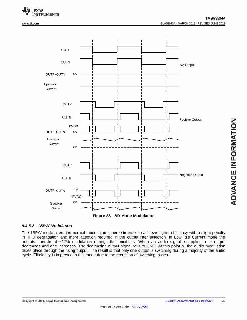
9.4.5.1 BD ModulationThis is a modulation scheme that allows operation without the classic LC reconstruction filter when the amp isdriving an inductive load with short speaker wires. Each output is switching from 0 volts to the supply voltage.The OUTPx and OUTNx are in phase with each other with no input so that there is little or no current in thespeaker. The duty cycle of OUTPx is greater than 50% and OUTNx is less than 50% for positive output voltages.The duty cycle of OUTPx is less than 50% and OUTNx is greater than 50% for negative output voltages. Thevoltage across the load sits at 0 V throughout most of the switching period, reducing the switching current, whichreduces any I2R losses in the load.
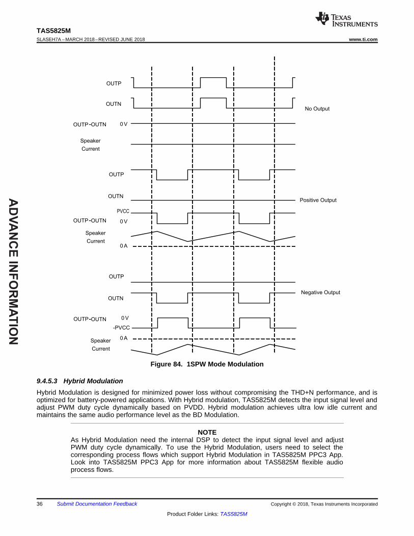
9.4.5.2 1SPW ModulationThe 1SPW mode alters the normal modulation scheme in order to achieve higher efficiency with a slight penaltyin THD degradation and more attention required in the output filter selection. In Low Idle Current mode theoutputs operate at ~17% modulation during idle conditions. When an audio signal is applied, one outputdecreases and one increases. The decreasing output signal rails to GND. At this point all the audio modulationtakes place through the rising output. The result is that only one output is switching during a majority of the audiocycle. Efficiency is improved in this mode due to the reduction of switching losses.
9.4.5.3 Hybrid ModulationHybrid Modulation is designed for minimized power loss without compromising the THD+N performance, and isoptimized for battery-powered applications. With Hybrid modulation, TAS5825M detects the input signal level andadjust PWM duty cycle dynamically based on PVDD. Hybrid modulation achieves ultra low idle current andmaintains the same audio performance level as the BD Modulation.
NOTEAs Hybrid Modulation need the internal DSP to detect the input signal level and adjustPWM duty cycle dynamically. To use the Hybrid Modulation, users need to select thecorresponding process flows which support Hybrid Modulation in TAS5825M PPC3 App.Look into TAS5825M PPC3 App for more information about TAS5825M flexible audioprocess flows.
9.5.1 I2 C Serial Communication BusThe device has a bidirectional serial control interface that is compatible with I2C bus protocol and supports 100and 400-kHz data transfer rates for random and sequential write and read operations as a slave device. Becausethe TAS5825M register map and DSP memory spans multi pages, the user should change from page to pagebefore writing individual register or DSP memory. Changing from page to page is accomplished via register 0 oneach page. This register value selects the page address, from 0 to 255. All registers listed in TAS5825MDatasheet belongs to Page 0
9.5.2 I2 C Slave AddressThe TAS5825M device has 7 bits for the slave address. The first five bits (MSBs) of the slave address arefactory preset to 10011(0x9x). The next two bits of address byte are the device select bits which can be user-defined by ADR pin in Table 4.
Table 4. I2 C Slave Address ConfigurationADR PIN Configuration MSBs User Define LSB
0 Ω to GND 1 0 0 1 1 0 0 R/W
1kΩ to GND 1 0 0 1 1 0 1 R/W
4.7kΩ to GND 1 0 0 1 1 1 0 R/W
15kΩ to GND 1 0 0 1 1 1 1 R/W
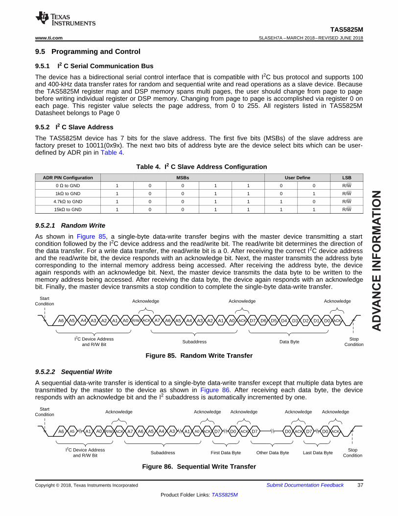
9.5.2.1 Random WriteAs shown in Figure 85, a single-byte data-write transfer begins with the master device transmitting a startcondition followed by the I2C device address and the read/write bit. The read/write bit determines the direction ofthe data transfer. For a write data transfer, the read/write bit is a 0. After receiving the correct I2C device addressand the read/write bit, the device responds with an acknowledge bit. Next, the master transmits the address bytecorresponding to the internal memory address being accessed. After receiving the address byte, the deviceagain responds with an acknowledge bit. Next, the master device transmits the data byte to be written to thememory address being accessed. After receiving the data byte, the device again responds with an acknowledgebit. Finally, the master device transmits a stop condition to complete the single-byte data-write transfer.
Figure 85. Random Write Transfer
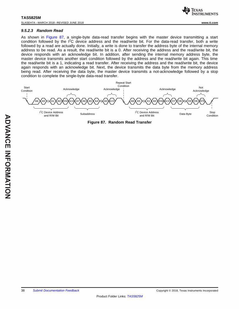
9.5.2.2 Sequential WriteA sequential data-write transfer is identical to a single-byte data-write transfer except that multiple data bytes aretransmitted by the master to the device as shown in Figure 86. After receiving each data byte, the deviceresponds with an acknowledge bit and the I2 subaddress is automatically incremented by one.
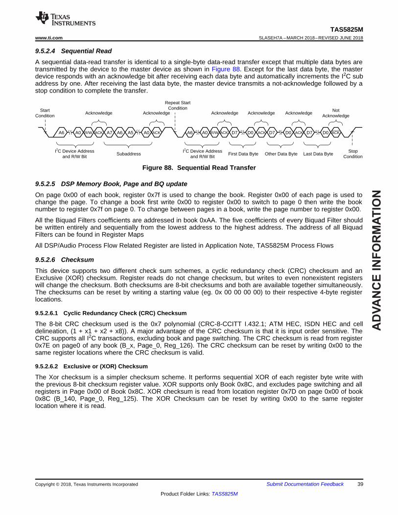
9.5.2.3 Random ReadAs shown in Figure 87, a single-byte data-read transfer begins with the master device transmitting a startcondition followed by the I2C device address and the read/write bit. For the data-read transfer, both a writefollowed by a read are actually done. Initially, a write is done to transfer the address byte of the internal memoryaddress to be read. As a result, the read/write bit is a 0. After receiving the address and the read/write bit, thedevice responds with an acknowledge bit. In addition, after sending the internal memory address byte, themaster device transmits another start condition followed by the address and the read/write bit again. This timethe read/write bit is a 1, indicating a read transfer. After receiving the address and the read/write bit, the deviceagain responds with an acknowledge bit. Next, the device transmits the data byte from the memory addressbeing read. After receiving the data byte, the master device transmits a not-acknowledge followed by a stopcondition to complete the single-byte data-read transfer.
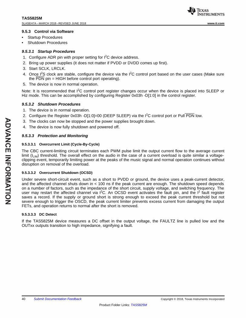
9.5.2.4 Sequential ReadA sequential data-read transfer is identical to a single-byte data-read transfer except that multiple data bytes aretransmitted by the device to the master device as shown in Figure 88. Except for the last data byte, the masterdevice responds with an acknowledge bit after receiving each data byte and automatically increments the I2C subaddress by one. After receiving the last data byte, the master device transmits a not-acknowledge followed by astop condition to complete the transfer.
Figure 88. Sequential Read Transfer
9.5.2.5 DSP Memory Book, Page and BQ updateOn page 0x00 of each book, register 0x7f is used to change the book. Register 0x00 of each page is used tochange the page. To change a book first write 0x00 to register 0x00 to switch to page 0 then write the booknumber to register 0x7f on page 0. To change between pages in a book, write the page number to register 0x00.
All the Biquad Filters coefficients are addressed in book 0xAA. The five coefficients of every Biquad Filter shouldbe written entirely and sequentially from the lowest address to the highest address. The address of all BiquadFilters can be found in Register Maps
All DSP/Audio Process Flow Related Register are listed in Application Note, TAS5825M Process Flows
9.5.2.6 ChecksumThis device supports two different check sum schemes, a cyclic redundancy check (CRC) checksum and anExclusive (XOR) checksum. Register reads do not change checksum, but writes to even nonexistent registerswill change the checksum. Both checksums are 8-bit checksums and both are available together simultaneously.The checksums can be reset by writing a starting value (eg. 0x 00 00 00 00) to their respective 4-byte registerlocations.
9.5.2.6.1 Cyclic Redundancy Check (CRC) Checksum
The 8-bit CRC checksum used is the 0x7 polynomial (CRC-8-CCITT I.432.1; ATM HEC, ISDN HEC and celldelineation, (1 + x1 + x2 + x8)). A major advantage of the CRC checksum is that it is input order sensitive. TheCRC supports all I2C transactions, excluding book and page switching. The CRC checksum is read from register0x7E on page0 of any book (B_x, Page_0, Reg_126). The CRC checksum can be reset by writing 0x00 to thesame register locations where the CRC checksum is valid.
9.5.2.6.2 Exclusive or (XOR) Checksum
The Xor checksum is a simpler checksum scheme. It performs sequential XOR of each register byte write withthe previous 8-bit checksum register value. XOR supports only Book 0x8C, and excludes page switching and allregisters in Page 0x00 of Book 0x8C. XOR checksum is read from location register 0x7D on page 0x00 of book0x8C (B_140, Page_0, Reg_125). The XOR Checksum can be reset by writing 0x00 to the same registerlocation where it is read.
9.5.3 Control via Software• Startup Procedures• Shutdown Procedures
9.5.3.1 Startup Procedures1. Configure ADR pin with proper setting for I2C device address.2. Bring up power supplies (it does not matter if PVDD or DVDD comes up first).3. Start SCLK, LRCLK.4. Once I2S clock are stable, configure the device via the I2C control port based on the user cases (Make sure
the PDN pin = HIGH before control port operating).5. The device is now in normal operation.
Note: It is recommended that I2C control port register changes occur when the device is placed into SLEEP orHiz mode. This can be accomplished by configuring Register 0x03h -D[1:0] in the control register.
9.5.3.2 Shutdown Procedures1. The device is in normal operation.2. Configure the Register 0x03h -D[1:0]=00 (DEEP SLEEP) via the I2C control port or Pull PDN low.3. The clocks can now be stopped and the power supplies brought down.4. The device is now fully shutdown and powered off.
9.5.3.3 Protection and Monitoring
9.5.3.3.1 Overcurrent Limit (Cycle-By-Cycle)
The CBC current-limiting circuit terminates each PWM pulse limit the output current flow to the average currentlimit (ILIM) threshold. The overall effect on the audio in the case of a current overload is quite similar a voltage-clipping event, temporarily limiting power at the peaks of the music signal and normal operation continues withoutdisruption on removal of the overload.
9.5.3.3.2 Overcurrent Shutdown (OCSD)
Under severe short-circuit event, such as a short to PVDD or ground, the device uses a peak-current detector,and the affected channel shuts down in < 100 ns if the peak current are enough. The shutdown speed dependson a number of factors, such as the impedance of the short circuit, supply voltage, and switching frequency. Theuser may restart the affected channel via I2C. An OCSD event activates the fault pin, and the I2 fault registersaves a record. If the supply or ground short is strong enough to exceed the peak current threshold but notsevere enough to trigger the OSCD, the peak current limiter prevents excess current from damaging the outputFETs, and operation returns to normal after the short is removed.
9.5.3.3.3 DC Detect
If the TAS5825M device measures a DC offset in the output voltage, the FAULTZ line is pulled low and theOUTxx outputs transition to high impedance, signifying a fault.
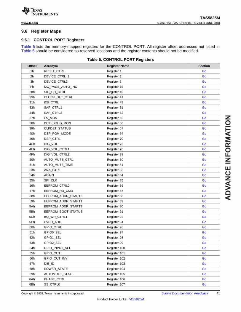
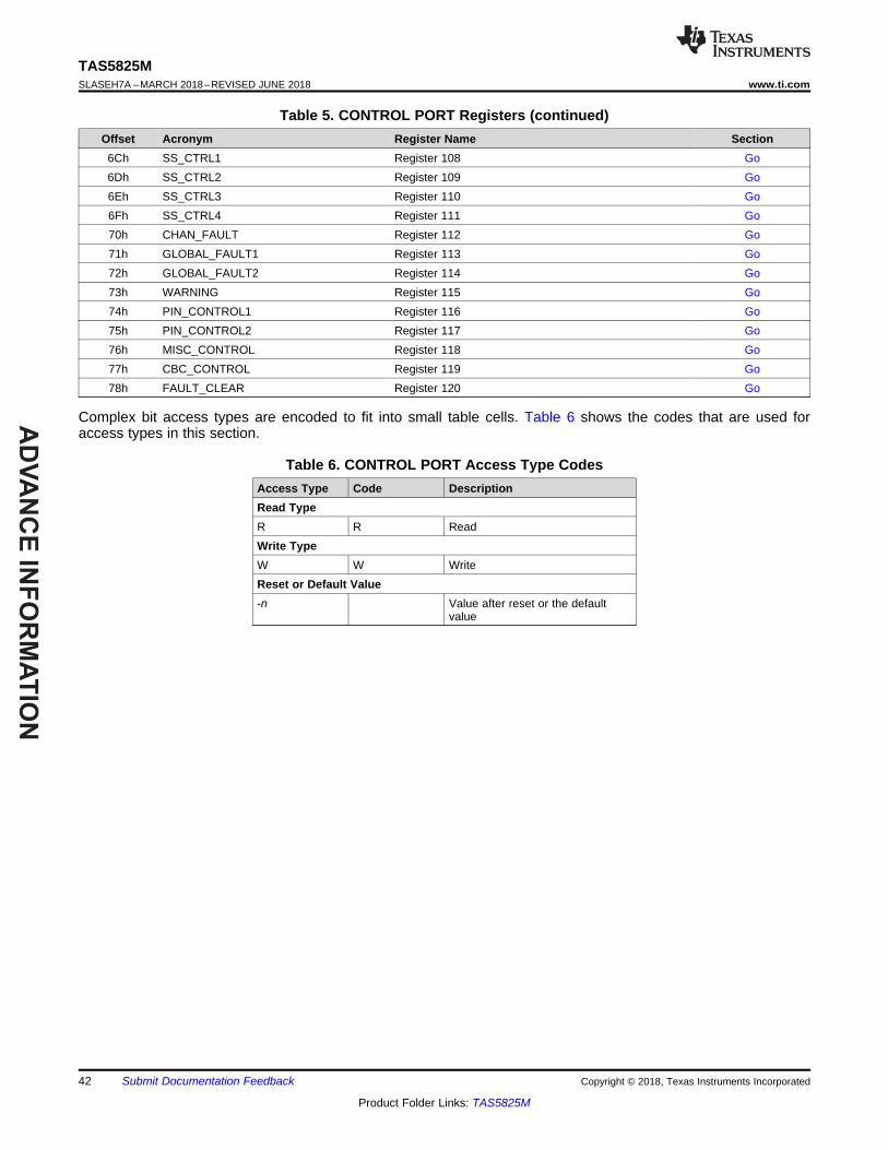
9.6.1 CONTROL PORT RegistersTable 5 lists the memory-mapped registers for the CONTROL PORT. All register offset addresses not listed inTable 5 should be considered as reserved locations and the register contents should not be modified.
Table 5. CONTROL PORT RegistersOffset Acronym Register Name Section
Complex bit access types are encoded to fit into small table cells. Table 6 shows the codes that are used foraccess types in this section.
Table 6. CONTROL PORT Access Type CodesAccess Type Code DescriptionRead TypeR R ReadWrite TypeW W WriteReset or Default Value-n Value after reset or the default
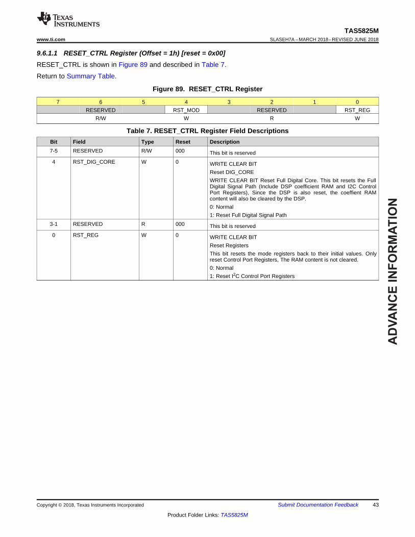
9.6.1.1 RESET_CTRL Register (Offset = 1h) [reset = 0x00]RESET_CTRL is shown in Figure 89 and described in Table 7.
Return to Summary Table.
Figure 89. RESET_CTRL Register
7 6 5 4 3 2 1 0RESERVED RST_MOD RESERVED RST_REG
R/W W R W
Table 7. RESET_CTRL Register Field DescriptionsBit Field Type Reset Description7-5 RESERVED R/W 000 This bit is reserved4 RST_DIG_CORE W 0 WRITE CLEAR BIT
Reset DIG_COREWRITE CLEAR BIT Reset Full Digital Core. This bit resets the FullDigital Signal Path (Include DSP coefficient RAM and I2C ControlPort Registers), Since the DSP is also reset, the coeffient RAMcontent will also be cleared by the DSP.0: Normal1: Reset Full Digital Signal Path
3-1 RESERVED R 000 This bit is reserved0 RST_REG W 0 WRITE CLEAR BIT
Reset RegistersThis bit resets the mode registers back to their initial values. Onlyreset Control Port Registers, The RAM content is not cleared.0: Normal1: Reset I2C Control Port Registers
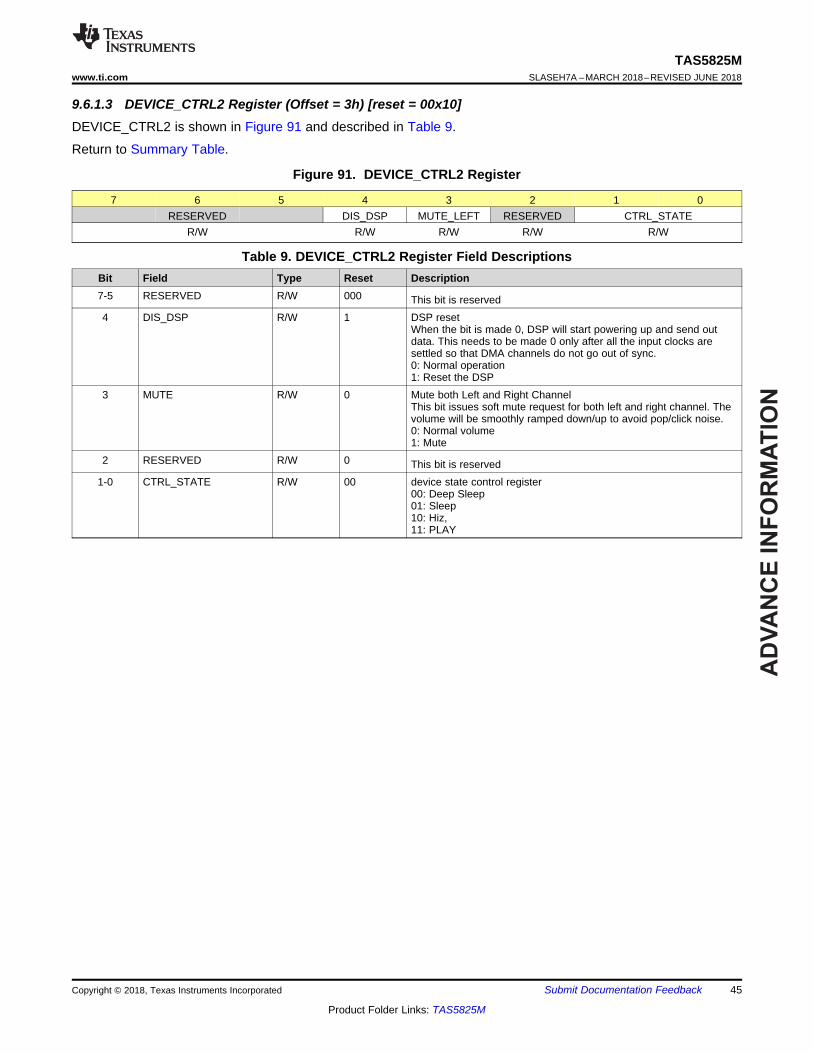
Table 9. DEVICE_CTRL2 Register Field DescriptionsBit Field Type Reset Description7-5 RESERVED R/W 000 This bit is reserved4 DIS_DSP R/W 1 DSP reset
When the bit is made 0, DSP will start powering up and send outdata. This needs to be made 0 only after all the input clocks aresettled so that DMA channels do not go out of sync.0: Normal operation1: Reset the DSP
3 MUTE R/W 0 Mute both Left and Right ChannelThis bit issues soft mute request for both left and right channel. Thevolume will be smoothly ramped down/up to avoid pop/click noise.0: Normal volume1: Mute
2 RESERVED R/W 0 This bit is reserved1-0 CTRL_STATE R/W 00 device state control register
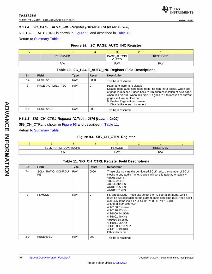
9.6.1.4 I2C_PAGE_AUTO_INC Register (Offset = Fh) [reset = 0x00]I2C_PAGE_AUTO_INC is shown in Figure 92 and described in Table 10.
Return to Summary Table.
Figure 92. I2C_PAGE_AUTO_INC Register
7 6 5 4 3 2 1 0RESERVED PAGE_AUTOIN
C_REGRESERVED
R/W R/W R/W
Table 10. I2C_PAGE_AUTO_INC Register Field DescriptionsBit Field Type Reset Description7-4 RESERVED R/W 0000 This bit is reserved3 PAGE_AUTOINC_REG R/W 0 Page auto increment disable
Disable page auto increment mode. for non -zero books. When endof page is reached it goes back to 8th address location of next pagewhen this bit is 0. When this bit is 1 it goes to 0 th location of currentpage itself like in older part.0: Enable Page auto increment1: Disable Page auto increment
2-0 RESERVED R/W 000 This bit is reserved
9.6.1.5 SIG_CH_CTRL Register (Offset = 28h) [reset = 0x00]SIG_CH_CTRL is shown in Figure 93 and described in Table 11.
Table 11. SIG_CH_CTRL Register Field DescriptionsBit Field Type Reset Description7-4 SCLK_RATIO_CONFIGU
RER/W 0000 These bits indicate the configured SCLK ratio, the number of SCLK
clocks in one audio frame. Device will set this ratio automatically.4'b0011:32FS4'b0101:64FS4'b0111:128FS4'b1001:256FS4'b1011:512FS
3 FSMODE R/W 0 FS Speed Mode These bits select the FS operation mode, whichmust be set according to the current audio sampling rate. Need set itmanually If the input Fs is 44.1kHz/88.2kHz/176.4kHz.4 'b0000 Auto detection4 'b0100 Reserved4 'b0110 32KHz4 'b1000 44.1KHz4 'b1001 48KHz4'b1010 88.2KHz4 'b1011 96KHz4 'b1100 176.4KHz4 'b1101 192KHzOthers Reserved
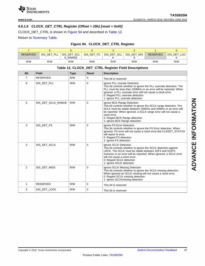
9.6.1.6 CLOCK_DET_CTRL Register (Offset = 29h) [reset = 0x00]CLOCK_DET_CTRL is shown in Figure 94 and described in Table 12.
Return to Summary Table.
Figure 94. CLOCK_DET_CTRL Register
7 6 5 4 3 2 1 0RESERVED DIS_DET_PLL DIS_DET_SCL
K_RANGEDIS_DET_FS DIS_DET_SCL
KDIS_DET_MIS
SRESERVED DIS_DET_LOC
KR/W R/W R/W R/W R/W R/W R/W R/W
Table 12. CLOCK_DET_CTRL Register Field DescriptionsBit Field Type Reset Description7 RESERVED R/W 0 This bit is reserved6 DIS_DET_PLL R/W 0 Ignore PLL overate Detection
This bit controls whether to ignore the PLL overrate detection. ThePLL must be slow than 150MHz or an error will be reported. Whenignored, a PLL overrate error will not cause a clock error.0: Regard PLL overrate detection1: Ignore PLL overrate detection
5 DIS_DET_SCLK_RANGE R/W 0 Ignore BCK Range DetectionThis bit controls whether to ignore the SCLK range detection. TheSCLK must be stable between 256KHz and 50MHz or an error willbe reported. When ignored, a SCLK range error will not cause aclock error.0: Regard BCK Range detection1: Ignore BCK Range detection
4 DIS_DET_FS R/W 0 Ignore FS Error DetectionThis bit controls whether to ignore the FS Error detection. Whenignored, FS error will not cause a clock error.But CLKDET_STATUSwill report fs error.0: Regard FS detection1: Ignore FS detection
3 DIS_DET_SCLK R/W 0 Ignore SCLK DetectionThis bit controls whether to ignore the SCLK detection againstLRCK. The SCLK must be stable between 32FS and 512FSinclusive or an error will be reported. When ignored, a SCLK errorwill not cause a clock error.0: Regard SCLK detection1: Ignore SCLK detection
2 DIS_DET_MISS R/W 0 Ignore SCLK Missing DetectionThis bit controls whether to ignore the SCLK missing detection.When ignored an SCLK missing will not cause a clock error.0: Regard SCLK missing detection1: Ignore SCLKmissing detection
1 RESERVED R/W 0 This bit is reserved0 DIS_DET_LOCK R/W 0 This bit is reserved
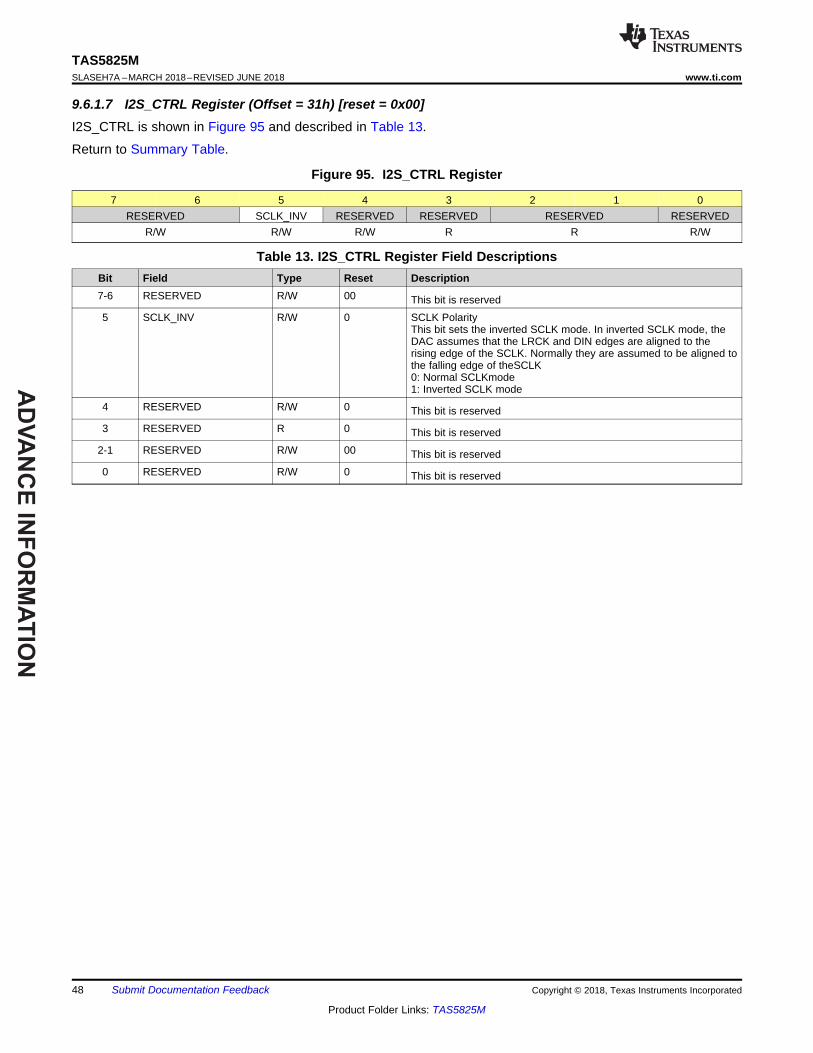
Table 13. I2S_CTRL Register Field DescriptionsBit Field Type Reset Description7-6 RESERVED R/W 00 This bit is reserved5 SCLK_INV R/W 0 SCLK Polarity
This bit sets the inverted SCLK mode. In inverted SCLK mode, theDAC assumes that the LRCK and DIN edges are aligned to therising edge of the SCLK. Normally they are assumed to be aligned tothe falling edge of theSCLK0: Normal SCLKmode1: Inverted SCLK mode
4 RESERVED R/W 0 This bit is reserved3 RESERVED R 0 This bit is reserved
2-1 RESERVED R/W 00 This bit is reserved0 RESERVED R/W 0 This bit is reserved
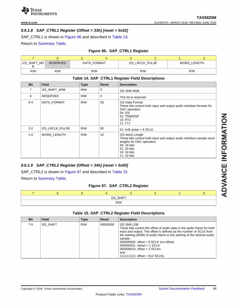
9.6.1.8 SAP_CTRL1 Register (Offset = 33h) [reset = 0x02]SAP_CTRL1 is shown in Figure 96 and described in Table 14.
Return to Summary Table.
Figure 96. SAP_CTRL1 Register
7 6 5 4 3 2 1 0I2S_SHIFT_MS
BRESERVED DATA_FORMAT I2S_LRCLK_PULSE WORD_LENGTH
R/W R/W R/W R/W R/W
Table 14. SAP_CTRL1 Register Field DescriptionsBit Field Type Reset Description7 I2S_SHIFT_MSB R/W 0 I2S Shift MSB6 RESERVED R/W 0 This bit is reserved
5-4 DATA_FORMAT R/W 00 I2S Data FormatThese bits control both input and output audio interface formats forDAC operation.00: I2S01: TDM/DSP10: RTJ11: LTJ
These bits control both input and output audio interface sample wordlengths for DAC operation.00: 16 bits01: 20 bits10: 24 bits11: 32 bits
9.6.1.9 SAP_CTRL2 Register (Offset = 34h) [reset = 0x00]SAP_CTRL2 is shown in Figure 97 and described in Table 15.
Return to Summary Table.
Figure 97. SAP_CTRL2 Register
7 6 5 4 3 2 1 0I2S_SHIFT
R/W
Table 15. SAP_CTRL2 Register Field DescriptionsBit Field Type Reset Description7-0 I2S_SHIFT R/W 00000000 I2S Shift LSB
These bits control the offset of audio data in the audio frame for bothinput and output. The offset is defined as the number of SCLK fromthe starting (MSB) of audio frame to the starting of the desired audiosample.000000000: offset = 0 SCLK (no offset)000000001: ofsset = 1 SCLK000000010: offset = 2 SCLKsand111111111: offset = 512 SCLKs
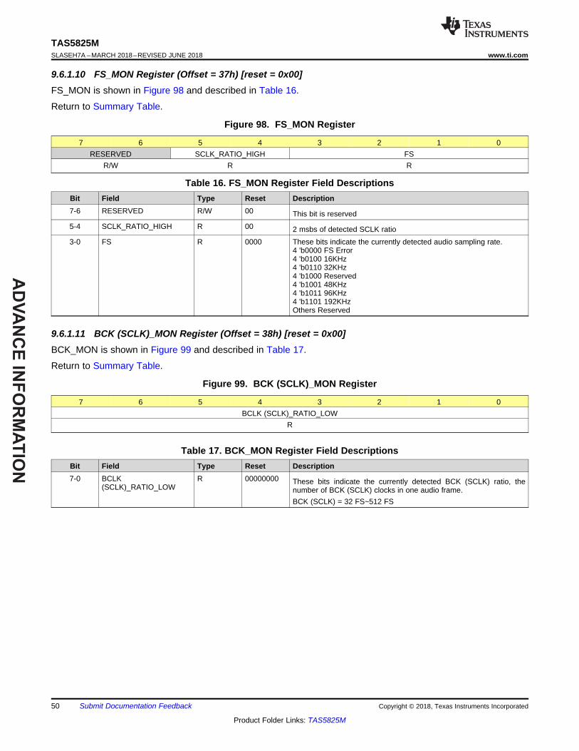
9.6.1.10 FS_MON Register (Offset = 37h) [reset = 0x00]FS_MON is shown in Figure 98 and described in Table 16.
Return to Summary Table.
Figure 98. FS_MON Register
7 6 5 4 3 2 1 0RESERVED SCLK_RATIO_HIGH FS
R/W R R
Table 16. FS_MON Register Field DescriptionsBit Field Type Reset Description7-6 RESERVED R/W 00 This bit is reserved5-4 SCLK_RATIO_HIGH R 00 2 msbs of detected SCLK ratio3-0 FS R 0000 These bits indicate the currently detected audio sampling rate.
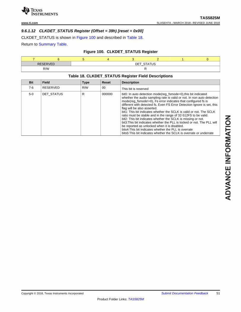
9.6.1.12 CLKDET_STATUS Register (Offset = 39h) [reset = 0x00]CLKDET_STATUS is shown in Figure 100 and described in Table 18.
Return to Summary Table.
Figure 100. CLKDET_STATUS Register
7 6 5 4 3 2 1 0RESERVED DET_STATUS
R/W R
Table 18. CLKDET_STATUS Register Field DescriptionsBit Field Type Reset Description7-6 RESERVED R/W 00 This bit is reserved5-0 DET_STATUS R 000000 bit0: In auto detection mode(reg_fsmode=0),this bit indicated
whether the audio sampling rate is valid or not. In non auto detectionmode(reg_fsmode!=0), Fs error indicates that configured fs isdifferent with detected fs. Even FS Error Detection Ignore is set, thisflag will be also asserted.bit1: This bit indicates whether the SCLK is valid or not. The SCLKratio must be stable and in the range of 32-512FS to be valid.bit2: This bit indicates whether the SCLK is missing or not.bit3:This bit indicates whether the PLL is locked or not. The PLL willbe reported as unlocked when it is disabled.bits4:This bit indicates whether the PLL is overratebits5:This bit indicates whether the SCLK is overrate or underrate
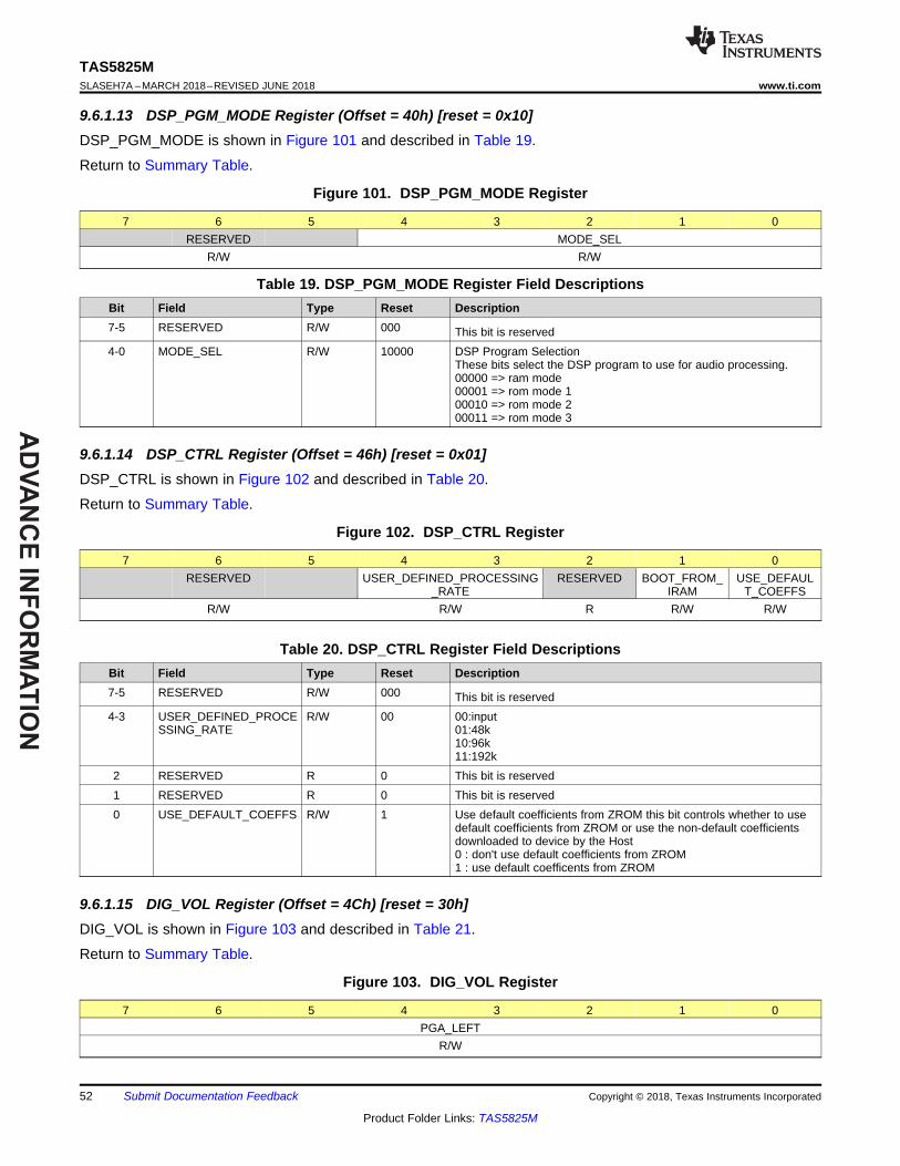
9.6.1.13 DSP_PGM_MODE Register (Offset = 40h) [reset = 0x10]DSP_PGM_MODE is shown in Figure 101 and described in Table 19.
Return to Summary Table.
Figure 101. DSP_PGM_MODE Register
7 6 5 4 3 2 1 0RESERVED MODE_SEL
R/W R/W
Table 19. DSP_PGM_MODE Register Field DescriptionsBit Field Type Reset Description7-5 RESERVED R/W 000 This bit is reserved4-0 MODE_SEL R/W 10000 DSP Program Selection
These bits select the DSP program to use for audio processing.00000 => ram mode00001 => rom mode 100010 => rom mode 200011 => rom mode 3
9.6.1.14 DSP_CTRL Register (Offset = 46h) [reset = 0x01]DSP_CTRL is shown in Figure 102 and described in Table 20.
Return to Summary Table.
Figure 102. DSP_CTRL Register
7 6 5 4 3 2 1 0RESERVED USER_DEFINED_PROCESSING
_RATERESERVED BOOT_FROM_
IRAMUSE_DEFAUL
T_COEFFSR/W R/W R R/W R/W
Table 20. DSP_CTRL Register Field DescriptionsBit Field Type Reset Description7-5 RESERVED R/W 000 This bit is reserved4-3 USER_DEFINED_PROCE
SSING_RATER/W 00 00:input
01:48k10:96k11:192k
2 RESERVED R 0 This bit is reserved1 RESERVED R 0 This bit is reserved0 USE_DEFAULT_COEFFS R/W 1 Use default coefficients from ZROM this bit controls whether to use
default coefficients from ZROM or use the non-default coefficientsdownloaded to device by the Host0 : don't use default coefficients from ZROM1 : use default coefficents from ZROM
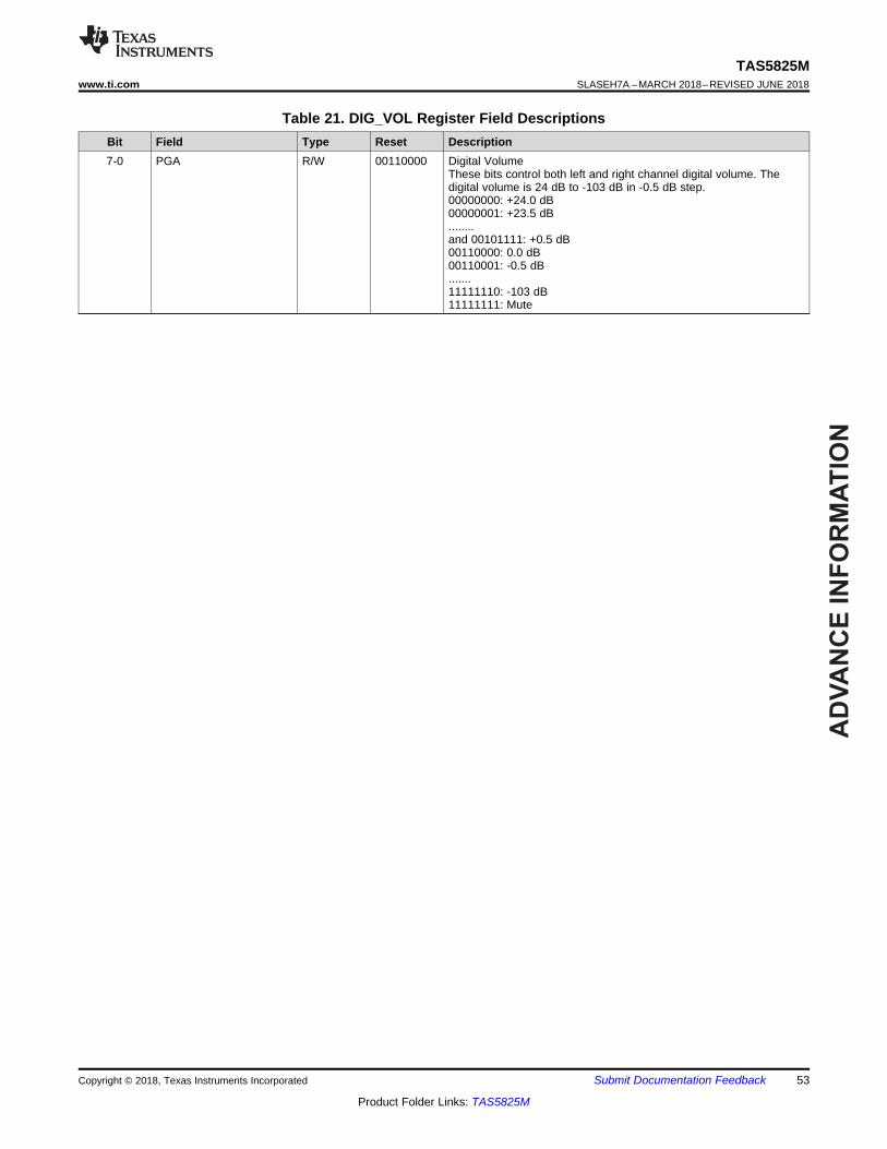
9.6.1.15 DIG_VOL Register (Offset = 4Ch) [reset = 30h]DIG_VOL is shown in Figure 103 and described in Table 21.
Table 21. DIG_VOL Register Field DescriptionsBit Field Type Reset Description7-0 PGA R/W 00110000 Digital Volume
These bits control both left and right channel digital volume. Thedigital volume is 24 dB to -103 dB in -0.5 dB step.00000000: +24.0 dB00000001: +23.5 dB........and 00101111: +0.5 dB00110000: 0.0 dB00110001: -0.5 dB.......11111110: -103 dB11111111: Mute
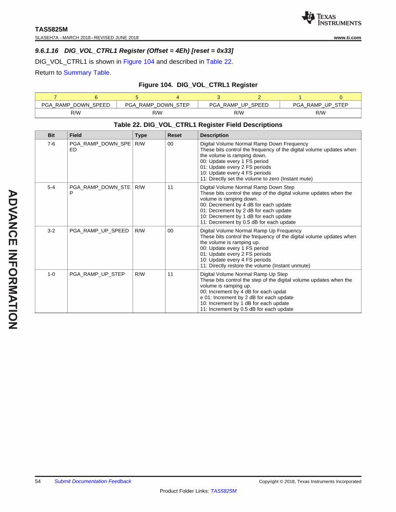
Table 22. DIG_VOL_CTRL1 Register Field DescriptionsBit Field Type Reset Description7-6 PGA_RAMP_DOWN_SPE
EDR/W 00 Digital Volume Normal Ramp Down Frequency
These bits control the frequency of the digital volume updates whenthe volume is ramping down.00: Update every 1 FS period01: Update every 2 FS periods10: Update every 4 FS periods11: Directly set the volume to zero (Instant mute)
5-4 PGA_RAMP_DOWN_STEP
R/W 11 Digital Volume Normal Ramp Down StepThese bits control the step of the digital volume updates when thevolume is ramping down.00: Decrement by 4 dB for each update01: Decrement by 2 dB for each update10: Decrement by 1 dB for each update11: Decrement by 0.5 dB for each update
3-2 PGA_RAMP_UP_SPEED R/W 00 Digital Volume Normal Ramp Up FrequencyThese bits control the frequency of the digital volume updates whenthe volume is ramping up.00: Update every 1 FS period01: Update every 2 FS periods10: Update every 4 FS periods11: Directly restore the volume (Instant unmute)
1-0 PGA_RAMP_UP_STEP R/W 11 Digital Volume Normal Ramp Up StepThese bits control the step of the digital volume updates when thevolume is ramping up.00: Increment by 4 dB for each update 01: Increment by 2 dB for each update10: Increment by 1 dB for each update11: Increment by 0.5 dB for each update
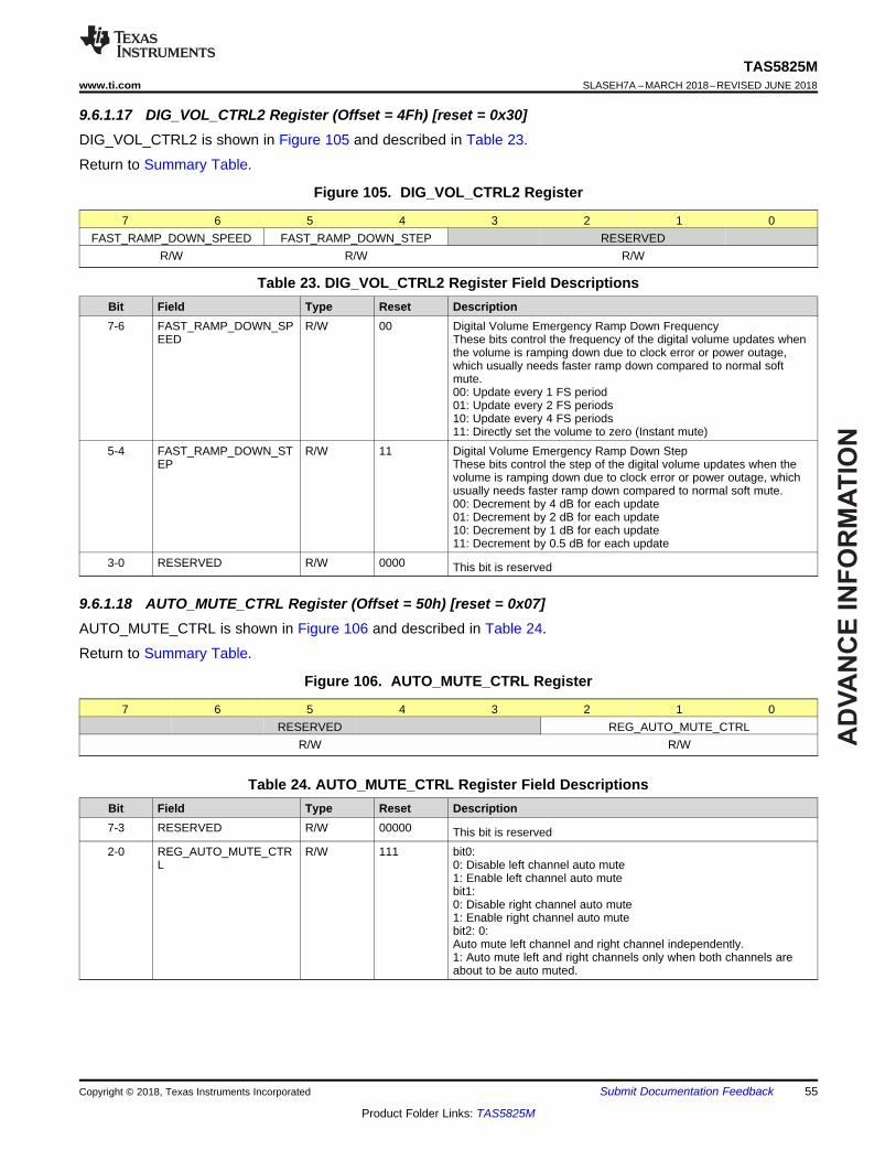
Table 23. DIG_VOL_CTRL2 Register Field DescriptionsBit Field Type Reset Description7-6 FAST_RAMP_DOWN_SP
EEDR/W 00 Digital Volume Emergency Ramp Down Frequency
These bits control the frequency of the digital volume updates whenthe volume is ramping down due to clock error or power outage,which usually needs faster ramp down compared to normal softmute.00: Update every 1 FS period01: Update every 2 FS periods10: Update every 4 FS periods11: Directly set the volume to zero (Instant mute)
5-4 FAST_RAMP_DOWN_STEP
R/W 11 Digital Volume Emergency Ramp Down StepThese bits control the step of the digital volume updates when thevolume is ramping down due to clock error or power outage, whichusually needs faster ramp down compared to normal soft mute.00: Decrement by 4 dB for each update01: Decrement by 2 dB for each update10: Decrement by 1 dB for each update11: Decrement by 0.5 dB for each update
3-0 RESERVED R/W 0000 This bit is reserved
9.6.1.18 AUTO_MUTE_CTRL Register (Offset = 50h) [reset = 0x07]AUTO_MUTE_CTRL is shown in Figure 106 and described in Table 24.
Return to Summary Table.
Figure 106. AUTO_MUTE_CTRL Register
7 6 5 4 3 2 1 0RESERVED REG_AUTO_MUTE_CTRL
R/W R/W
Table 24. AUTO_MUTE_CTRL Register Field DescriptionsBit Field Type Reset Description7-3 RESERVED R/W 00000 This bit is reserved2-0 REG_AUTO_MUTE_CTR
LR/W 111 bit0:
0: Disable left channel auto mute1: Enable left channel auto mutebit1:0: Disable right channel auto mute1: Enable right channel auto mutebit2: 0:Auto mute left channel and right channel independently.1: Auto mute left and right channels only when both channels areabout to be auto muted.
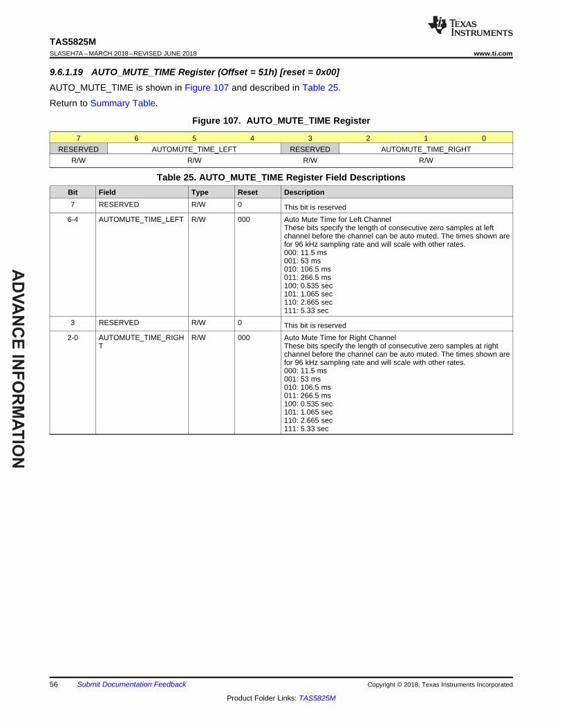
Table 25. AUTO_MUTE_TIME Register Field DescriptionsBit Field Type Reset Description7 RESERVED R/W 0 This bit is reserved
6-4 AUTOMUTE_TIME_LEFT R/W 000 Auto Mute Time for Left ChannelThese bits specify the length of consecutive zero samples at leftchannel before the channel can be auto muted. The times shown arefor 96 kHz sampling rate and will scale with other rates.000: 11.5 ms001: 53 ms010: 106.5 ms011: 266.5 ms100: 0.535 sec101: 1.065 sec110: 2.665 sec111: 5.33 sec
3 RESERVED R/W 0 This bit is reserved2-0 AUTOMUTE_TIME_RIGH
TR/W 000 Auto Mute Time for Right Channel
These bits specify the length of consecutive zero samples at rightchannel before the channel can be auto muted. The times shown arefor 96 kHz sampling rate and will scale with other rates.000: 11.5 ms001: 53 ms010: 106.5 ms011: 266.5 ms100: 0.535 sec101: 1.065 sec110: 2.665 sec111: 5.33 sec
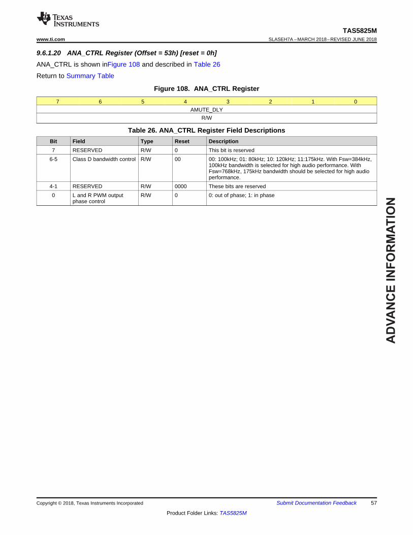
9.6.1.20 ANA_CTRL Register (Offset = 53h) [reset = 0h]ANA_CTRL is shown inFigure 108 and described in Table 26
Return to Summary Table
Figure 108. ANA_CTRL Register
7 6 5 4 3 2 1 0AMUTE_DLY
R/W
Table 26. ANA_CTRL Register Field DescriptionsBit Field Type Reset Description7 RESERVED R/W 0 This bit is reserved
6-5 Class D bandwidth control R/W 00 00: 100kHz; 01: 80kHz; 10: 120kHz; 11:175kHz. With Fsw=384kHz,100kHz bandwidth is selected for high audio performance. WithFsw=768kHz, 175kHz bandwidth should be selected for high audioperformance.
4-1 RESERVED R/W 0000 These bits are reserved0 L and R PWM output
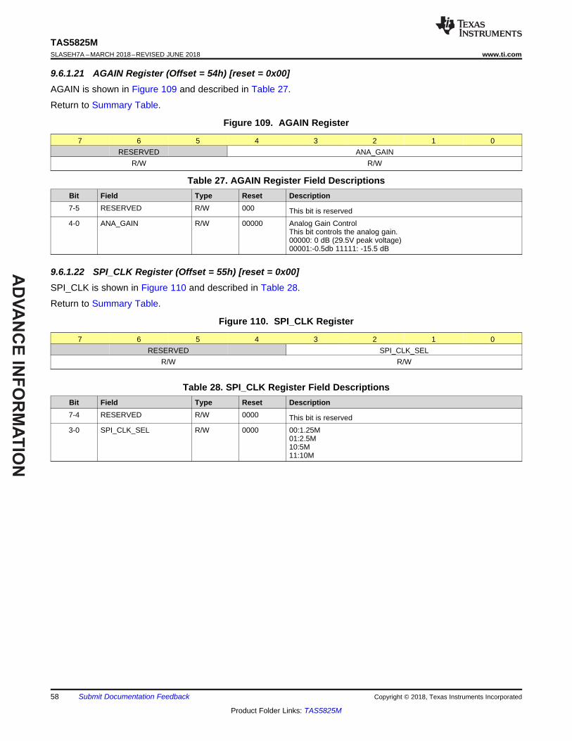
9.6.1.21 AGAIN Register (Offset = 54h) [reset = 0x00]AGAIN is shown in Figure 109 and described in Table 27.
Return to Summary Table.
Figure 109. AGAIN Register
7 6 5 4 3 2 1 0RESERVED ANA_GAIN
R/W R/W
Table 27. AGAIN Register Field DescriptionsBit Field Type Reset Description7-5 RESERVED R/W 000 This bit is reserved4-0 ANA_GAIN R/W 00000 Analog Gain Control
This bit controls the analog gain.00000: 0 dB (29.5V peak voltage)00001:-0.5db 11111: -15.5 dB
9.6.1.22 SPI_CLK Register (Offset = 55h) [reset = 0x00]SPI_CLK is shown in Figure 110 and described in Table 28.
Return to Summary Table.
Figure 110. SPI_CLK Register
7 6 5 4 3 2 1 0RESERVED SPI_CLK_SEL
R/W R/W
Table 28. SPI_CLK Register Field DescriptionsBit Field Type Reset Description7-4 RESERVED R/W 0000 This bit is reserved3-0 SPI_CLK_SEL R/W 0000 00:1.25M
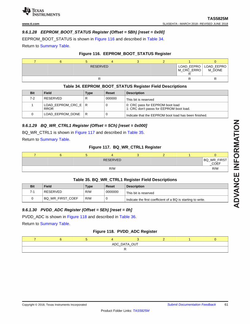
9.6.1.28 EEPROM_BOOT_STATUS Register (Offset = 5Bh) [reset = 0x00]EEPROM_BOOT_STATUS is shown in Figure 116 and described in Table 34.
Return to Summary Table.
Figure 116. EEPROM_BOOT_STATUS Register
7 6 5 4 3 2 1 0RESERVED LOAD_EEPRO
M_CRC_ERROR
LOAD_EEPROM_DONE
R R R
Table 34. EEPROM_BOOT_STATUS Register Field DescriptionsBit Field Type Reset Description7-2 RESERVED R 000000 This bit is reserved1 LOAD_EEPROM_CRC_E
RRORR 0 0: CRC pass for EEPROM boot load
1: CRC don't passs for EEPROM boot load.0 LOAD_EEPROM_DONE R 0 Indicate that the EEPROM boot load has been finished.
9.6.1.29 BQ_WR_CTRL1 Register (Offset = 5Ch) [reset = 0x000]BQ_WR_CTRL1 is shown in Figure 117 and described in Table 35.
Return to Summary Table.
Figure 117. BQ_WR_CTRL1 Register
7 6 5 4 3 2 1 0RESERVED BQ_WR_FIRST
_COEFR/W R/W
Table 35. BQ_WR_CTRL1 Register Field DescriptionsBit Field Type Reset Description7-1 RESERVED R/W 0000000 This bit is reserved0 BQ_WR_FIRST_COEF R/W 0 Indicate the first coefficient of a BQ is starting to write.
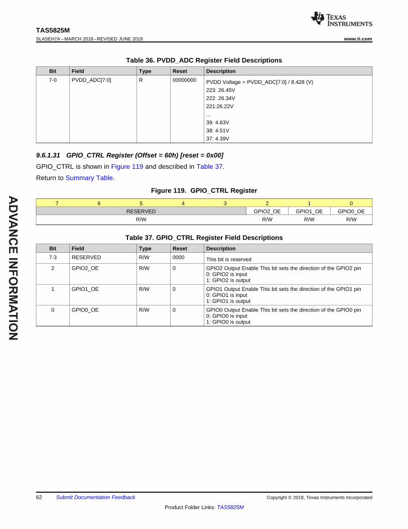
9.6.1.30 PVDD_ADC Register (Offset = 5Eh) [reset = 0h]PVDD_ADC is shown in Figure 118 and described in Table 36.
Table 37. GPIO_CTRL Register Field DescriptionsBit Field Type Reset Description7-3 RESERVED R/W 0000 This bit is reserved2 GPIO2_OE R/W 0 GPIO2 Output Enable This bit sets the direction of the GPIO2 pin
0: GPIO2 is input1: GPIO2 is output
1 GPIO1_OE R/W 0 GPIO1 Output Enable This bit sets the direction of the GPIO1 pin0: GPIO1 is input1: GPIO1 is output
0 GPIO0_OE R/W 0 GPIO0 Output Enable This bit sets the direction of the GPIO0 pin0: GPIO0 is input1: GPIO0 is output
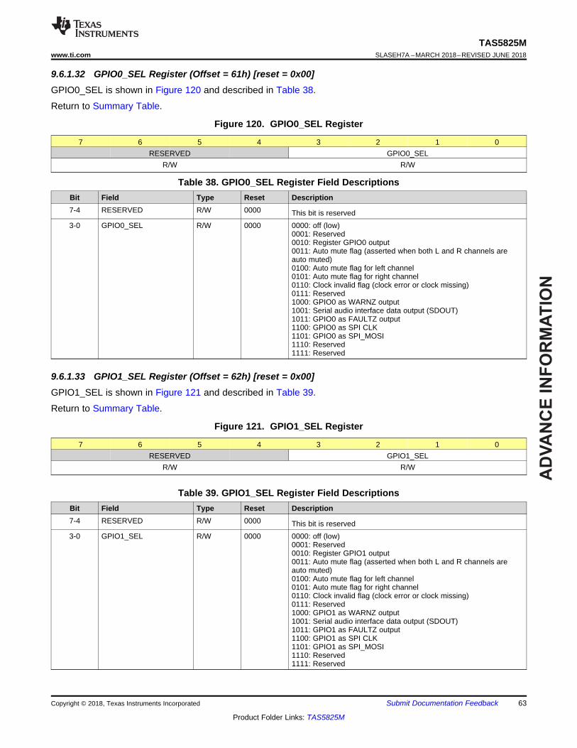
9.6.1.32 GPIO0_SEL Register (Offset = 61h) [reset = 0x00]GPIO0_SEL is shown in Figure 120 and described in Table 38.
Return to Summary Table.
Figure 120. GPIO0_SEL Register
7 6 5 4 3 2 1 0RESERVED GPIO0_SEL
R/W R/W
Table 38. GPIO0_SEL Register Field DescriptionsBit Field Type Reset Description7-4 RESERVED R/W 0000 This bit is reserved3-0 GPIO0_SEL R/W 0000 0000: off (low)
0001: Reserved0010: Register GPIO0 output0011: Auto mute flag (asserted when both L and R channels areauto muted)0100: Auto mute flag for left channel0101: Auto mute flag for right channel0110: Clock invalid flag (clock error or clock missing)0111: Reserved1000: GPIO0 as WARNZ output1001: Serial audio interface data output (SDOUT)1011: GPIO0 as FAULTZ output1100: GPIO0 as SPI CLK1101: GPIO0 as SPI_MOSI1110: Reserved1111: Reserved
9.6.1.33 GPIO1_SEL Register (Offset = 62h) [reset = 0x00]GPIO1_SEL is shown in Figure 121 and described in Table 39.
Return to Summary Table.
Figure 121. GPIO1_SEL Register
7 6 5 4 3 2 1 0RESERVED GPIO1_SEL
R/W R/W
Table 39. GPIO1_SEL Register Field DescriptionsBit Field Type Reset Description7-4 RESERVED R/W 0000 This bit is reserved3-0 GPIO1_SEL R/W 0000 0000: off (low)
0001: Reserved0010: Register GPIO1 output0011: Auto mute flag (asserted when both L and R channels areauto muted)0100: Auto mute flag for left channel0101: Auto mute flag for right channel0110: Clock invalid flag (clock error or clock missing)0111: Reserved1000: GPIO1 as WARNZ output1001: Serial audio interface data output (SDOUT)1011: GPIO1 as FAULTZ output1100: GPIO1 as SPI CLK1101: GPIO1 as SPI_MOSI1110: Reserved1111: Reserved
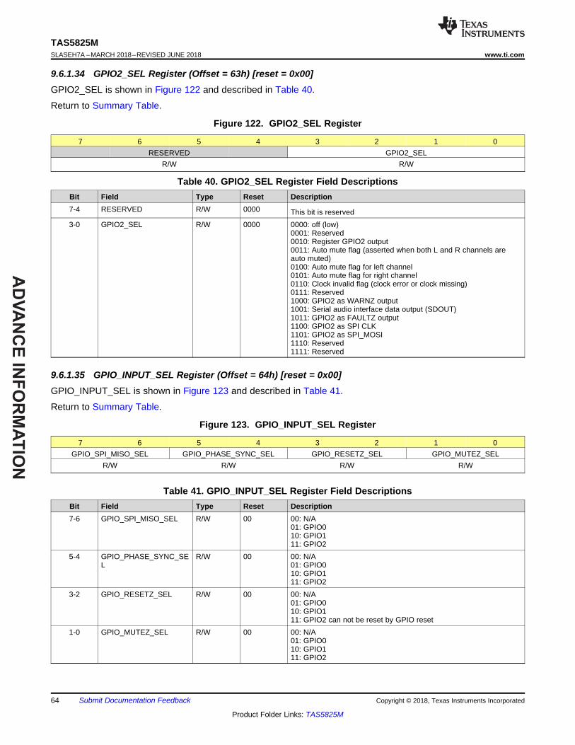
9.6.1.34 GPIO2_SEL Register (Offset = 63h) [reset = 0x00]GPIO2_SEL is shown in Figure 122 and described in Table 40.
Return to Summary Table.
Figure 122. GPIO2_SEL Register
7 6 5 4 3 2 1 0RESERVED GPIO2_SEL
R/W R/W
Table 40. GPIO2_SEL Register Field DescriptionsBit Field Type Reset Description7-4 RESERVED R/W 0000 This bit is reserved3-0 GPIO2_SEL R/W 0000 0000: off (low)
0001: Reserved0010: Register GPIO2 output0011: Auto mute flag (asserted when both L and R channels areauto muted)0100: Auto mute flag for left channel0101: Auto mute flag for right channel0110: Clock invalid flag (clock error or clock missing)0111: Reserved1000: GPIO2 as WARNZ output1001: Serial audio interface data output (SDOUT)1011: GPIO2 as FAULTZ output1100: GPIO2 as SPI CLK1101: GPIO2 as SPI_MOSI1110: Reserved1111: Reserved
9.6.1.35 GPIO_INPUT_SEL Register (Offset = 64h) [reset = 0x00]GPIO_INPUT_SEL is shown in Figure 123 and described in Table 41.
9.6.1.36 GPIO_OUT Register (Offset = 65h) [reset = 0x00]GPIO_OUT is shown in Figure 124 and described in Table 42.
Return to Summary Table.
Figure 124. GPIO_OUT Register
7 6 5 4 3 2 1 0RESERVED GPIO_OUT
R/W R/W
Table 42. GPIO_OUT Register Field DescriptionsBit Field Type Reset Description7-3 RESERVED R/W 00000 This bit is reserved2-0 GPIO_OUT R/W 000 bit0: GPIO0 output
bit1: GPIO1 outputbit2: GPIO2 output
9.6.1.37 GPIO_OUT_INV Register (Offset = 66h) [reset = 0x00]GPIO_OUT_INV is shown in Figure 125 and described in Table 43.
Return to Summary Table.
Figure 125. GPIO_OUT_INV Register
7 6 5 4 3 2 1 0RESERVED GPIO_OUT
R/W R/W
Table 43. GPIO_OUT_INV Register Field DescriptionsBit Field Type Reset Description7-3 RESERVED R/W 00000 This bit is reserved2-0 GPIO_OUT R/W 000 bit0: GPIO0 output invert
9.6.1.40 AUTOMUTE_STATE Register (Offset = 69h) [reset = 0x00]AUTOMUTE_STATE is shown in Figure 128 and described in Table 46.
Return to Summary Table.
Figure 128. AUTOMUTE_STATE Register
7 6 5 4 3 2 1 0RESERVED ZERO_RIGHT_
MONZERO_LEFT_
MONR R R
Table 46. AUTOMUTE_STATE Register Field DescriptionsBit Field Type Reset Description7-2 RESERVED R 000000 This bit is reserved1 ZERO_RIGHT_MON R 0 This bit indicates the auto mute status for right channel.
0: Not auto muted1: Auto muted
0 ZERO_LEFT_MON R 0 This bit indicates the auto mute status for left channel.0: Not auto muted1: Auto muted
9.6.1.41 PHASE_CTRL Register (Offset = 6Ah) [reset = 0]PHASE_CTRL is shown in Figure 129 and described in Table 47.
Return to Summary Table.
Figure 129. PHASE_CTRL Register
7 6 5 4 3 2 1 0RESERVED RAMP_PHASE_SEL PHASE_SYNC
_SELPHASE_SYNC
_ENR/W R/W R/W R/W
Table 47. PHASE_CTRL Register Field DescriptionsBit Field Type Reset Description7-4 RESERVED R/W 0000 This bit is reserved3-2 RAMP_PHASE_SEL R/W 00 select ramp clock phase when multi devices integrated in one
system to reduce EMI and peak supply peak current, it isrecomended set all devices the same RAMP frequency and samespread spectrum. it must be set before driving device into PLAYmode if this feature is needed.2'b00: phase 02'b01: phase 12'b10: phase 22'b11: phase 3 all of above have a 45 degree of phase shift
9.6.1.42 RAMP_SS_CTRL0 Register (Offset = 6Bh) [reset = 0x00]RAMP_SS_CTRL0 is shown in Figure 130 and described in Table 48.
Return to Summary Table.
Figure 130. SS_CTRL0 Register
7 6 5 4 3 2 1 0RESERVED RESERVED SS_PRE_DIV_
SELSS_MANUAL_
MODERESERVED SS_RDM_EN SS_TRI_EN
R/W R/W R/W R/W R/W R/W R/W
Table 48. RAMP_SS_CTRL0 Register Field DescriptionsBit Field Type Reset Description7 RESERVED R/W 0 This bit is reserved6 RESERVED R/W 0 This bit is reserved5 SS_PRE_DIV_SEL R/W 0 select pll clock divide 2 as source clock in manual mode4 SS_MANUAL_MODE R/W 0 set ramp ss controller to manual mode
3-2 RESERVED R/W 00 This bit is reserved1 SS_RDM_EN R/W 0 random SS enable0 SS_TRI_EN R/W 0 triangle SS enable
9.6.1.43 SS_CTRL1 Register (Offset = 6Ch) [reset = 0x00]SS_CTRL1 is shown in Figure 131 and described in Table 49.
Return to Summary Table.
Figure 131. SS_CTRL1 Register
7 6 5 4 3 2 1 0RESERVED SS_RDM_CTRL SS_TRI_CTRL
R/W R/W R/W
Table 49. SS_CTRL1 Register Field DescriptionsBit Field Type Reset Description7 RESERVED R/W 0 This bit is reserved
6-4 SS_RDM_CTRL R/W 000 Add Dither3-0 SS_TRI_CTRL R/W 0000 triangle SS frequency and range control
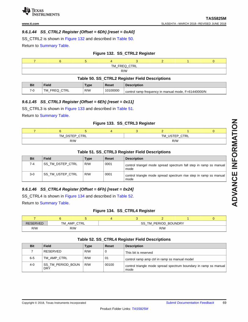
9.6.1.44 SS_CTRL2 Register (Offset = 6Dh) [reset = 0xA0]SS_CTRL2 is shown in Figure 132 and described in Table 50.
Return to Summary Table.
Figure 132. SS_CTRL2 Register
7 6 5 4 3 2 1 0TM_FREQ_CTRL
R/W
Table 50. SS_CTRL2 Register Field DescriptionsBit Field Type Reset Description7-0 TM_FREQ_CTRL R/W 10100000 control ramp frequency in manual mode, F=61440000/N
9.6.1.45 SS_CTRL3 Register (Offset = 6Eh) [reset = 0x11]SS_CTRL3 is shown in Figure 133 and described in Table 51.
Return to Summary Table.
Figure 133. SS_CTRL3 Register
7 6 5 4 3 2 1 0TM_DSTEP_CTRL TM_USTEP_CTRL
R/W R/W
Table 51. SS_CTRL3 Register Field DescriptionsBit Field Type Reset Description7-4 SS_TM_DSTEP_CTRL R/W 0001 control triangel mode spread spectrum fall step in ramp ss manual
mode3-0 SS_TM_USTEP_CTRL R/W 0001 control triangle mode spread spectrum rise step in ramp ss manual
mode
9.6.1.46 SS_CTRL4 Register (Offset = 6Fh) [reset = 0x24]SS_CTRL4 is shown in Figure 134 and described in Table 52.
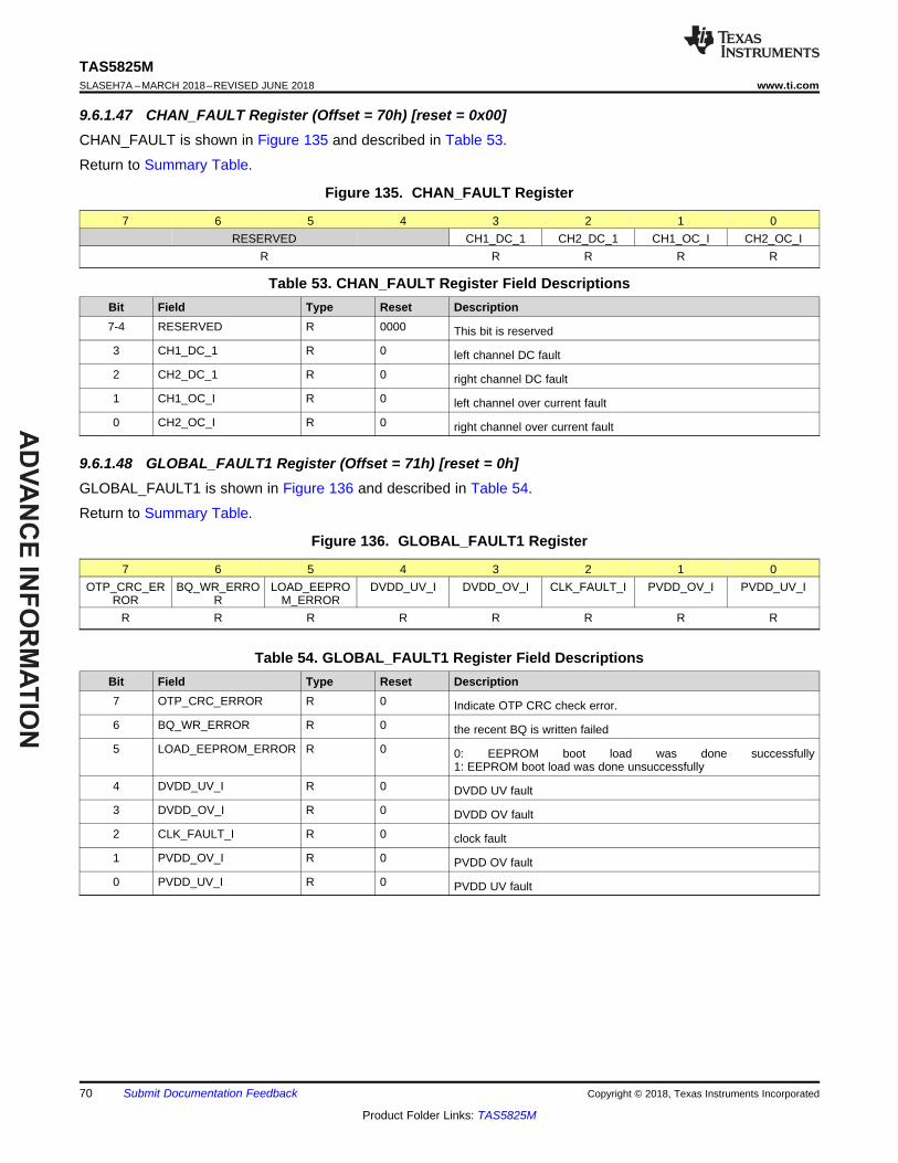
Table 53. CHAN_FAULT Register Field DescriptionsBit Field Type Reset Description7-4 RESERVED R 0000 This bit is reserved3 CH1_DC_1 R 0 left channel DC fault2 CH2_DC_1 R 0 right channel DC fault1 CH1_OC_I R 0 left channel over current fault0 CH2_OC_I R 0 right channel over current fault
9.6.1.48 GLOBAL_FAULT1 Register (Offset = 71h) [reset = 0h]GLOBAL_FAULT1 is shown in Figure 136 and described in Table 54.
Table 54. GLOBAL_FAULT1 Register Field DescriptionsBit Field Type Reset Description7 OTP_CRC_ERROR R 0 Indicate OTP CRC check error.6 BQ_WR_ERROR R 0 the recent BQ is written failed5 LOAD_EEPROM_ERROR R 0 0: EEPROM boot load was done successfully
1: EEPROM boot load was done unsuccessfully4 DVDD_UV_I R 0 DVDD UV fault3 DVDD_OV_I R 0 DVDD OV fault2 CLK_FAULT_I R 0 clock fault1 PVDD_OV_I R 0 PVDD OV fault0 PVDD_UV_I R 0 PVDD UV fault
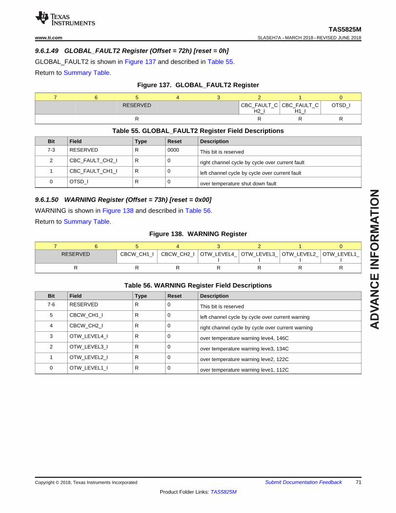
9.6.1.49 GLOBAL_FAULT2 Register (Offset = 72h) [reset = 0h]GLOBAL_FAULT2 is shown in Figure 137 and described in Table 55.
Return to Summary Table.
Figure 137. GLOBAL_FAULT2 Register
7 6 5 4 3 2 1 0RESERVED CBC_FAULT_C
H2_ICBC_FAULT_C
H1_IOTSD_I
R R R R
Table 55. GLOBAL_FAULT2 Register Field DescriptionsBit Field Type Reset Description7-3 RESERVED R 0000 This bit is reserved2 CBC_FAULT_CH2_I R 0 right channel cycle by cycle over current fault1 CBC_FAULT_CH1_I R 0 left channel cycle by cycle over current fault0 OTSD_I R 0 over temperature shut down fault
9.6.1.50 WARNING Register (Offset = 73h) [reset = 0x00]WARNING is shown in Figure 138 and described in Table 56.
Table 56. WARNING Register Field DescriptionsBit Field Type Reset Description7-6 RESERVED R 0 This bit is reserved5 CBCW_CH1_I R 0 left channel cycle by cycle over current warning4 CBCW_CH2_I R 0 right channel cycle by cycle over current warning3 OTW_LEVEL4_I R 0 over temperature warning leve4, 146C2 OTW_LEVEL3_I R 0 over temperature warning leve3, 134C1 OTW_LEVEL2_I R 0 over temperature warning leve2, 122C0 OTW_LEVEL1_I R 0 over temperature warning leve1, 112C
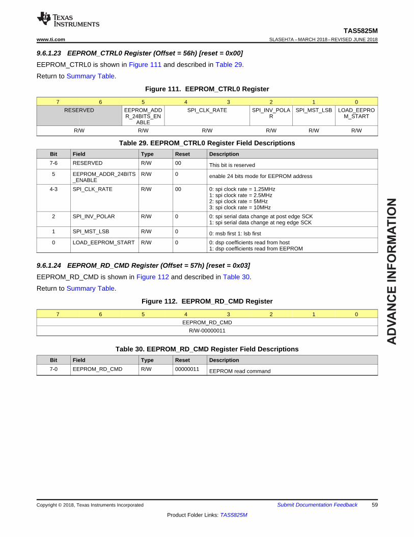
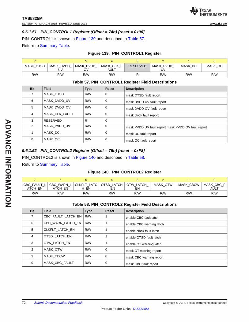
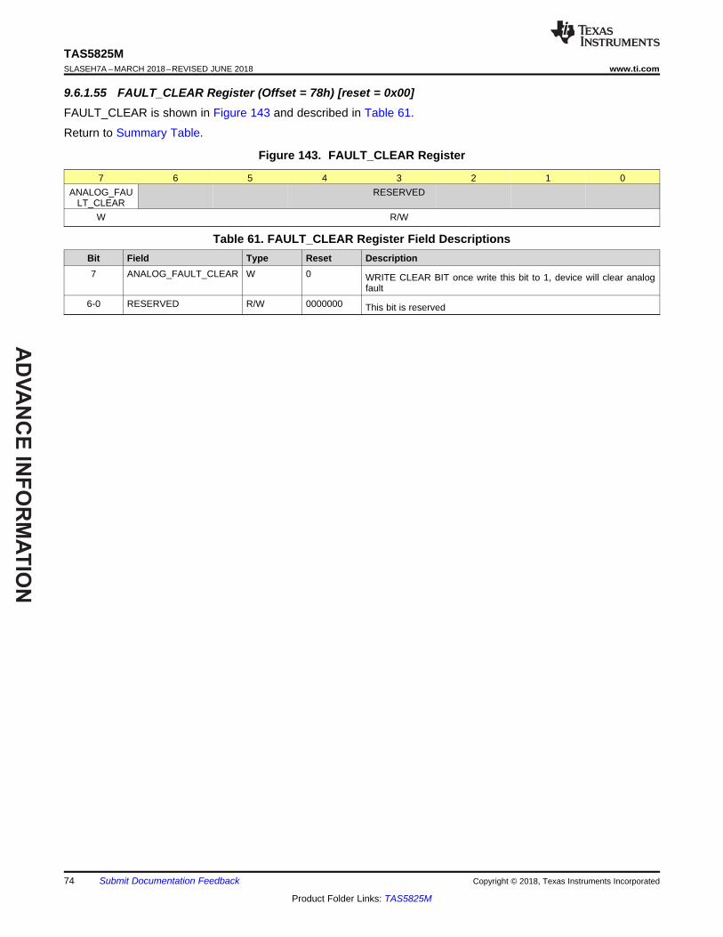
9.6.1.55 FAULT_CLEAR Register (Offset = 78h) [reset = 0x00]FAULT_CLEAR is shown in Figure 143 and described in Table 61.
Return to Summary Table.
Figure 143. FAULT_CLEAR Register
7 6 5 4 3 2 1 0ANALOG_FAU
LT_CLEARRESERVED
W R/W
Table 61. FAULT_CLEAR Register Field DescriptionsBit Field Type Reset Description7 ANALOG_FAULT_CLEAR W 0 WRITE CLEAR BIT once write this bit to 1, device will clear analog
fault6-0 RESERVED R/W 0000000 This bit is reserved
NOTEInformation in the following applications sections is not part of the TI componentspecification, and TI does not warrant its accuracy or completeness. TI’s customers areresponsible for determining suitability of components for their purposes. Customers shouldvalidate and test their design implementation to confirm system functionality.
10.1 Application InformationThis section details the information required to configure the device for several popular configurations andprovides guidance on integrating the TAS5825M device into the larger system.
10.1.1 Bootstrap CapacitorsThe output stage of the TAS5825M uses a high-side NMOS driver, rather than a PMOS driver. To generate thegate driver voltage for the high-side NMOS, a bootstrap capacitor for each output terminal acts as a floatingpower supply for the switching cycle. Use 0.22-µF capacitors to connect the appropriate output pin (OUT_X) tothe bootstrap pin (BST_X). For example, connect a 0.22-µF capacitor between OUT_A and BST_A forbootstrapping the A channel. Similarly, connect another 0.22-µF capacitor between the OUT_B and BST_B pinsfor the B channel inverting output.
10.1.2 Power Supply DecouplingTo ensure high efficiency, low THD, and high PSRR, proper power supply decoupling is necessary. Noisetransients on the power supply lines are short duration voltage spikes. These spikes can contain frequencycomponents that extend into the hundreds of megahertz. The power supply input must be decoupled with somegood quality, low ESL, Low ESR capacitors larger than 22 µF. These capacitors bypasses low frequency noise tothe ground plane. For high frequency decoupling, place 1-µF or 0.1-µF capacitors as close as possible to thePVDD pins of the device.
10.1.3 Output EMI FilteringThe TAS5825M device is often used with a low-pass filter, which is used to filter out the carrier frequency of thePWM modulated output. This filter is frequently referred to as the L-C Filter, due to the presence of an inductiveelement L and a capacitive element C to make up the 2-pole filter.
The L-C filter removes the carrier frequency, reducing electromagnetic emissions and smoothing the currentwaveform which is drawn from the power supply. The presence and size of the L-C filter is determined by severalsystem level constraints. In some low-power use cases that have no other circuits which are sensitive to EMI, asimple ferrite bead or a ferrite bead plus a capacitor can replace the tradition large inductor and capacitor thatare commonly used. In other high-power applications, large toroid inductors are required for maximum power andfilm capacitors can be used due to audio characteristics. Refer to the application report Class-D LC Filter Design(SLOA119) for a detailed description on the proper component selection and design of an L-C filter based uponthe desired load and response.
10.2 Typical Applications
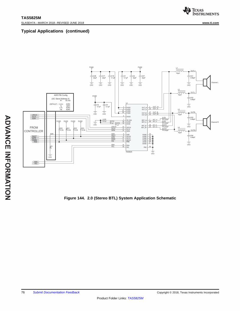
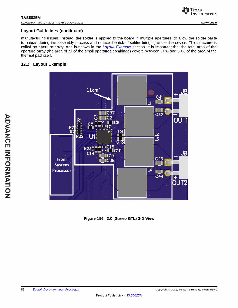
10.2.1 2.0 (Stereo BTL) SystemIn the 2.0 system, two channels are presented to the amplifier via the digital input signal. These two channels areamplified and then sent to two separate speakers. In some cases, the amplified signal is further separated basedupon frequency by a passive crossover network after the L-C filter. Even so, the application is considered 2.0.
Most commonly, the two channels are a pair of signals called a stereo pair, with one channel containing theaudio for the left channel and the other channel containing the audio for the right channel. While certainly the twochannels can contain any two audio channels, such as two surround channels of a multi-channel speakersystem, the most popular occurrence in two channels systems is a stereo pair.
Figure 144 shows the 2.0 (Stereo BTL) system application.
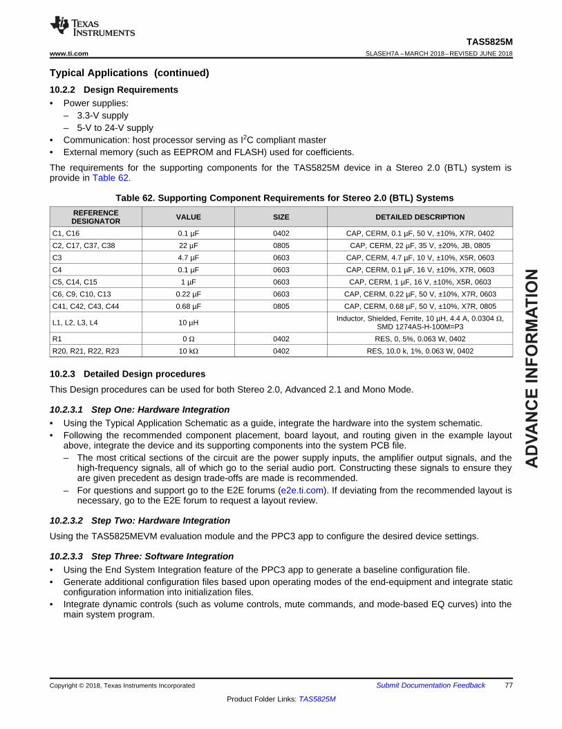
10.2.3 Detailed Design proceduresThis Design procedures can be used for both Stereo 2.0, Advanced 2.1 and Mono Mode.
10.2.3.1 Step One: Hardware Integration• Using the Typical Application Schematic as a guide, integrate the hardware into the system schematic.• Following the recommended component placement, board layout, and routing given in the example layout
above, integrate the device and its supporting components into the system PCB file.– The most critical sections of the circuit are the power supply inputs, the amplifier output signals, and the
high-frequency signals, all of which go to the serial audio port. Constructing these signals to ensure theyare given precedent as design trade-offs are made is recommended.
– For questions and support go to the E2E forums (e2e.ti.com). If deviating from the recommended layout isnecessary, go to the E2E forum to request a layout review.
10.2.3.2 Step Two: Hardware IntegrationUsing the TAS5825MEVM evaluation module and the PPC3 app to configure the desired device settings.
10.2.3.3 Step Three: Software Integration• Using the End System Integration feature of the PPC3 app to generate a baseline configuration file.• Generate additional configuration files based upon operating modes of the end-equipment and integrate static
configuration information into initialization files.• Integrate dynamic controls (such as volume controls, mute commands, and mode-based EQ curves) into the
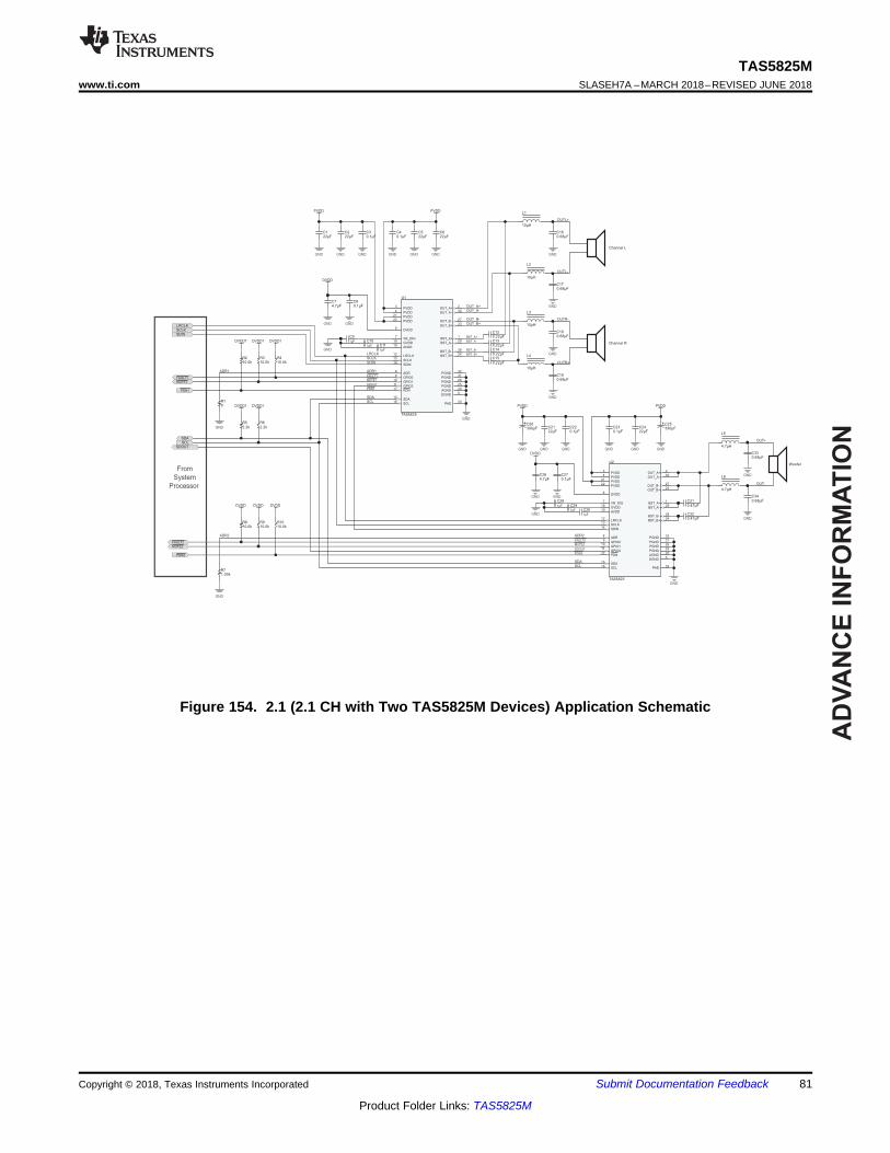
10.2.6 Advanced 2.1 System (Two TAS5825M Devices)In higher performance systems, the subwoofer output can be enhanced using digital audio processing as wasdone in the high-frequency channels. To accomplish this, two TAS5825M devices are used - one for the highfrequency left and right speakers and one for the mono subwoofer speaker. In this system, the audio signal canbe sent from the TAS5825M device through the SDOUT pin. Alternatively, the subwoofer amplifier can acceptthe same digital input as the stereo, which might come from a central systems processor.Figure 154 shows the2.1 (Stereo BTL with Two TAS5825M devices) system application.
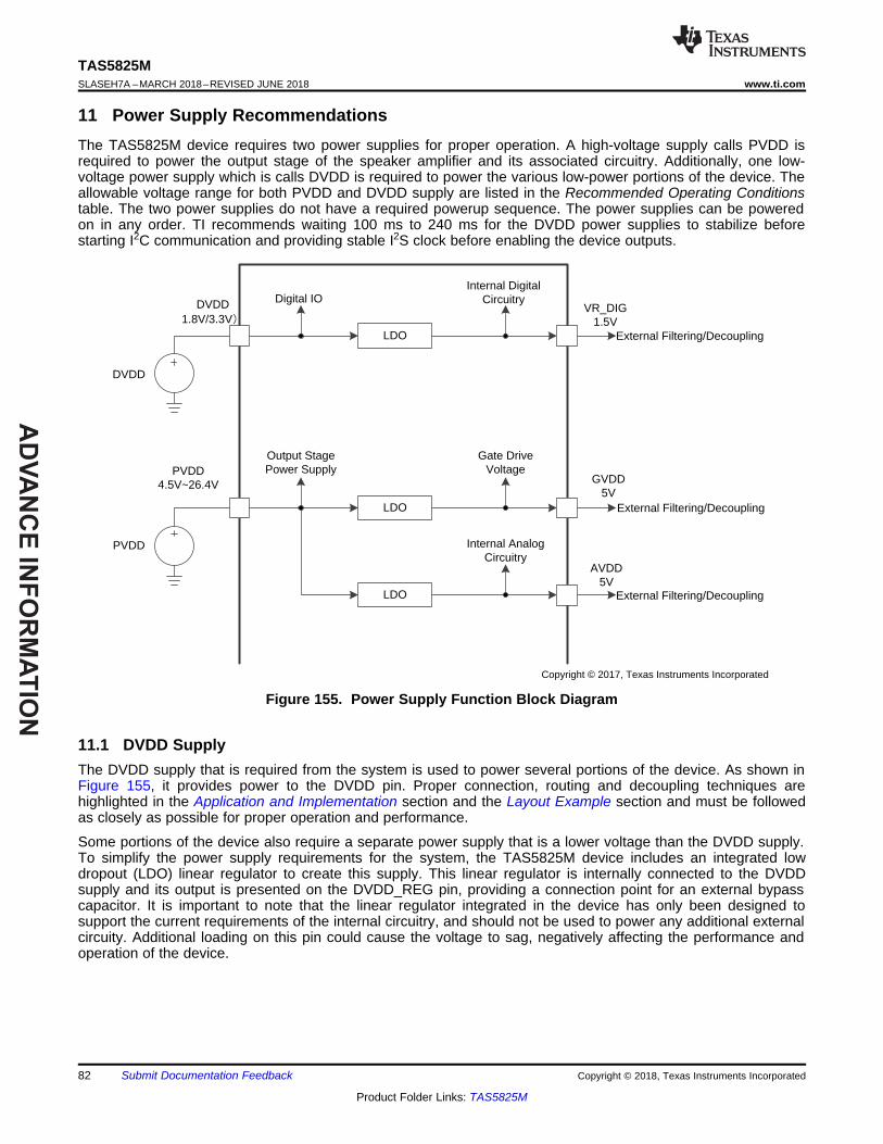
11 Power Supply RecommendationsThe TAS5825M device requires two power supplies for proper operation. A high-voltage supply calls PVDD isrequired to power the output stage of the speaker amplifier and its associated circuitry. Additionally, one low-voltage power supply which is calls DVDD is required to power the various low-power portions of the device. Theallowable voltage range for both PVDD and DVDD supply are listed in the Recommended Operating Conditionstable. The two power supplies do not have a required powerup sequence. The power supplies can be poweredon in any order. TI recommends waiting 100 ms to 240 ms for the DVDD power supplies to stabilize beforestarting I2C communication and providing stable I2S clock before enabling the device outputs.
Figure 155. Power Supply Function Block Diagram
11.1 DVDD SupplyThe DVDD supply that is required from the system is used to power several portions of the device. As shown inFigure 155, it provides power to the DVDD pin. Proper connection, routing and decoupling techniques arehighlighted in the Application and Implementation section and the Layout Example section and must be followedas closely as possible for proper operation and performance.
Some portions of the device also require a separate power supply that is a lower voltage than the DVDD supply.To simplify the power supply requirements for the system, the TAS5825M device includes an integrated lowdropout (LDO) linear regulator to create this supply. This linear regulator is internally connected to the DVDDsupply and its output is presented on the DVDD_REG pin, providing a connection point for an external bypasscapacitor. It is important to note that the linear regulator integrated in the device has only been designed tosupport the current requirements of the internal circuitry, and should not be used to power any additional externalcircuity. Additional loading on this pin could cause the voltage to sag, negatively affecting the performance andoperation of the device.
11.2 PVDD SupplyThe output stage of the speaker amplifier drives the load using the PVDD supply. This is the power supply whichprovides the drive current to the load during playback. Proper connection, routing, and decoupling techniques arehighlighted in the TAS5825MEVM and must be followed as closely as possible for proper operation andperformance. Due to the high-voltage switching of the output stage, it is particularly important to properlydecouple the output power stages in the manner described in the TAS5825M device Application andImplementation. Lack of proper decoupling, like that shown in the Application and Implementation, results involtage spikes which can damage the device.
A separate power supply is required to drive the gates of the MOSFETs used in the output stage of the speakeramplifier. This power supply is derived from the PVDD supply via an integrated linear regulator. A GVDD pin isprovided for the attachment of decoupling capacitor for the gate drive voltage regulator. It is important to notethat the linear regulator integrated in the device has only been designed to support the current requirements ofthe internal circuitry, and should not be used to power any additional external circuitry. Additional loading on thispin could cause the voltage to sag, negatively affecting the performance and operation of the device.
Another separate power supply is derived from the PVDD supply via an integrated linear regulator is AVDD.AVDD pin is provided for the attachment of decoupling capacitor for the TAS5825M internal circuitry. It isimportant to note that the linear regulator integrated in the device has only been designed to support the currentrequirements of the internal circuitry, and should not be used to power any additional external circuitry. Additionalloading on this pin could cause the voltage to sag, negatively affecting the performance and operation of thedevice.
12.1.1 General Guidelines for Audio AmplifiersAudio amplifiers which incorporate switching output stages must have special attention paid to their layout andthe layout of the supporting components used around them. The system level performance metrics, includingthermal performance, electromagnetic compliance (EMC), device reliability, and audio performance are allaffected by the device and supporting component layout.
Ideally, the guidance provided in the applications section with regard to device and component selection can befollowed by precise adherence to the layout guidance shown in the Layout Example section. These examplesrepresent exemplary baseline balance of the engineering trade-offs involved with lying out the device. Thesedesigns can be modified slightly as needed to meet the needs of a given application. In some applications, forinstance, solution size can be compromised to improve thermal performance through the use of additionalcontiguous copper neat the device. Conversely, EMI performance can be prioritized over thermal performance byrouting on internal traces and incorporating a via picket-fence and additional filtering components. In all cases, itis recommended to start from the guidance shown in the Layout Example section and work with TI fieldapplication engineers or through the E2E community to modify it based upon the application specific goals.
12.1.2 Importance of PVDD Bypass Capacitor Placement on PVDD NetworkPlacing the bypassing and decoupling capacitors close to supply has long been understood in the industry. Thisapplies to DVDD, AVDD, GVDD and PVDD. However, the capacitors on the PVDD net for the TAS5782M devicedeserve special attention.
The small bypass capacitors on the PVDD lines of the DUT must be placed as close to the PVDD pins aspossible. Not only dose placing these device far away from the pins increase the electromagnetic interference inthe system, but doing so can also negatively affect the reliability of the device. Placement of these componentstoo far from the TAS5782M device can cause ringing on the output pins that can cause the voltage on the outputpin to exceed the maximum allowable ratings shown in the Absolute Maximum Ratings table, damaging thedeice . For that reason, the capacitors on the PVDD net must be no further away from their associated PVDDpins than what is shown in the example layouts in the Layout Example section.
12.1.3 Optimizing Thermal PerformanceFollow the layout example shown in the Figure 156 to achieve the best balance of solution size, thermal, audio,and electromagnetic performance. In some cases, deviation from this guidance can be required due to designconstraints which cannot be avoided. In these instances, the system designer should ensure that the heat canget out of the device and into the ambient air surrounding the device. Fortunately, the heat created in the devicenaturally travels away from the device and into the lower temperature structures around the device.
12.1.3.1 Device, Copper, and Component LayoutPrimarily, the goal of the PCB design is to minimize the thermal impedance in the path to those cooler structures.These tips should be followed to achieve that goal:• Avoid placing other heat producing components or structures near the amplifier (including above or below in
the end equipment).• If possible, use a higher layer count PCB to provide more heat sinking capability for the TAS5825M device
and to prevent traces and copper signal and power planes from breaking up the contiguous copper on the topand bottom layer.
• Place the TAS5825M device away from the edge of the PCB when possible to ensure that the heat can travelaway from the device on all four sides.
• Avoid cutting off the flow of heat from the TAS5825M device to the surrounding areas with traces or viastrings. Instead, route traces perpendicular to the device and line up vias in columns which are perpendicularto the device.
• Unless the area between two pads of a passive component is large enough to allow copper to flow inbetween the two pads, orient it so that the narrow end of the passive component is facing the TAS5782Mdevice.
• Because the ground pins are the best conductors of heat in the package, maintain a contiguous ground plane
Layout Guidelines (continued)from the ground pins to the PCB area surrounding the device for as many of the ground pins as possible.
12.1.3.2 Stencil PatternThe recommended drawings for the TAS5825M device PCB foot print and associated stencil pattern are shownat the end of this document in the package addendum. Additionally, baseline recommendations for the viaarrangement under and around the device are given as a starting point for the PCB design. This guidance isprovided to suit the majority of manufacturing capabilities in the industry and prioritizes manufacturability over allother performance criteria. In elevated ambient temperature or under high-power dissipation use-cases, thisguidance may be too conservative and advanced PCB design techniques may be used to improve thermalperformance of the system.
NOTEThe customer must verify that deviation from the guidance shown in the packageaddendum, including the deviation explained in this section, meets the customer’s quality,reliability, and manufacturability goals.
12.1.3.2.1 PCB footprint and Via Arrangement
The PCB footprint (also known as a symbol or land pattern) communicates to the PCB fabrication vendor theshape and position of the copper patterns to which the TAS5825M device will be soldered. This footprint can befollowed directly from the guidance in the package addendum at the end of this data sheet. It is important tomake sure that the thermal pad, which connects electrically and thermally to the PowerPAD™ of the TAS5825Mdevice, be made no smaller than what is specified in the package addendum. This ensures that the TAS5825Mdevice has the largest interface possible to move heat from the device to the board.
The via pattern shown in the package addendum provides an improved interface to carry the heat from thedevice through to the layers of the PCB, because small diameter plated vias (with minimally-sized annular rings)present a low thermal-impedance path from the device into the PCB. Once into the PCB, the heat travels awayfrom the device and into the surrounding structures and air. By increasing the number of vias, as shown in theLayout Example section, this interface can benefit from improved thermal performance.
NOTEVias can obstruct heat flow if they are not constructed properly.
More notes on the construction and placement of vias are as follows:• Remove thermal reliefs on thermal vias, because they impede the flow of heat through the via.• Vias filled with thermally conductive material are best, but a simple plated via can be used to avoid the
additional cost of filled vias.• The diameter of the drull must be 8 mm or less. Also, the distance between the via barrel and the surrounding
planes should be minimized to help heat flow from the via into the surrounding copper material. In all cases,minimum spacing should be determined by the voltages present on the planes surrounding the via andminimized wherever possible.
• Vias should be arranged in columns, which extend in a line radially from the heat source to the surroundingarea. This arrangement is shown in the Layout Example section.
• Ensure that vias do not cut off power current flow from the power supply through the planes on internallayers. If needed, remove some vias that are farthest from the TAS5825M device to open up the current pathto and from the device.
12.1.3.2.2 Solder Stencil
During the PCB assembly process, a piece of metal called a stencil on top of the PCB and deposits solder pasteon the PCB wherever there is an opening (called an aperture) in the stencil. The stencil determines the quantityand the location of solder paste that is applied to the PCB in the electronic manufacturing process. In mostcases, the aperture for each of the component pads is almost the same size as the pad itself. However, thethermal pad on the PCB is large and depositing a large, single deposition of solder paste would lead to
Layout Guidelines (continued)manufacturing issues. Instead, the solder is applied to the board in multiple apertures, to allow the solder pasteto outgas during the assembly process and reduce the risk of solder bridging under the device. This structure iscalled an aperture array, and is shown in the Layout Example section. It is important that the total area of theaperture array (the area of all of the small apertures combined) covers between 70% and 80% of the area of thethermal pad itself.
13.1.1 Device NomenclatureThe glossary listed in the Glossary section is a general glossary with commonly used acronyms and words whichare defined in accordance with a broad TI initiative to comply with industry standards such as JEDEC, IPC, IEEE,and others. The glossary provided in this section defines words, phrases, and acronyms that are unique to thisproduct and documentation, collateral, or support tools and software used with this product. For any additionalquestions regarding definitions and terminology, please see the e2e Audio Amplfier Forum.
Bridge tied load (BTL) is an output configuration in which one terminal of the speaker is connected to one half-bridge and the other terminal is connected to another half-bridge.
DUT refers to a device under test to differentiate one device from another.
Closed-loop architecture describes a topology in which the amplifier monitors the output terminals, comparingthe output signal to the input signal and attempts to correct for non-linearities in the output.
Dynamic controls are those which are changed during normal use by either the system or the end-user.
GPIO is a general purpose input/output pin. It is a highly configurable, bi-directional digital pin which can performmany functions as required by the system.
Host processor (also known as System Processor, Scalar, Host, or System Controller) refers to devicewhich serves as a central system controller, providing control information to devices connected to it as well asgathering audio source data from devices upstream from it and distributing it to other devices. This device oftenconfigures the controls of the audio processing devices (like the ) in the audio path in order to optimize the audiooutput of a loudspeaker based on frequency response, time alignment, target sound pressure level, safeoperating area of the system, and user preference.
HybridFlow uses components which are built in RAM and components which are built in ROM to make aconfigurable device that is easier to use than a fully-programmable device while remaining flexible enough to beused in several applications
Maximum continuous output power refers to the maximum output power that the amplifier can continuouslydeliver without shutting down when operated in a 25°C ambient temperature. Testing is performed for the periodof time required that their temperatures reach thermal equilibrium and are no longer increasing
Parallel bridge tied load (PBTL) is an output configuration in which one terminal of the speaker is connected totwo half-bridges which have been placed in parallel and the other terminal is connected to another pair of halfbridges placed in parallel
rDS(on) is a measure of the on-resistance of the MOSFETs used in the output stage of the amplifier.
Static controls/Static configurations are controls which do not change while the system is in normal use.
Vias are copper-plated through-hole in a PCB.
13.1.2 Development SupportFor RDGUI software, please consult your local field support engineer.
13.2 Receiving Notification of Documentation UpdatesTo receive notification of documentation updates, navigate to the device product folder on ti.com. In the upperright corner, click on Alert me to register and receive a weekly digest of any product information that haschanged. For change details, review the revision history included in any revised document.
13.3 Community ResourcesThe following links connect to TI community resources. Linked contents are provided "AS IS" by the respectivecontributors. They do not constitute TI specifications and do not necessarily reflect TI's views; see TI's Terms ofUse.
TI E2E™ Online Community TI's Engineer-to-Engineer (E2E) Community. Created to foster collaborationamong engineers. At e2e.ti.com, you can ask questions, share knowledge, explore ideas and helpsolve problems with fellow engineers.
Design Support TI's Design Support Quickly find helpful E2E forums along with design support tools andcontact information for technical support.
13.4 TrademarksPowerPAD, E2E are trademarks of Texas Instruments.
13.5 Electrostatic Discharge CautionThese devices have limited built-in ESD protection. The leads should be shorted together or the device placed in conductive foamduring storage or handling to prevent electrostatic damage to the MOS gates.
13.6 GlossarySLYZ022 — TI Glossary.
This glossary lists and explains terms, acronyms, and definitions.
14 Mechanical, Packaging, and Orderable InformationThe following pages include mechanical, packaging, and orderable information. This information is the mostcurrent data available for the designated devices. This data is subject to change without notice and revision ofthis document. For browser-based versions of this data sheet, refer to the left-hand navigation.
PTAS5825MRHBR ACTIVE VQFN RHB 32 3000 TBD Call TI Call TI -25 to 85
TAS5825MRHBR PREVIEW VQFN RHB 32 3000 TBD Call TI Call TI -25 to 85
TAS5825MRHBT PREVIEW VQFN RHB 32 250 TBD Call TI Call TI -25 to 85 (1) The marketing status values are defined as follows:ACTIVE: Product device recommended for new designs.LIFEBUY: TI has announced that the device will be discontinued, and a lifetime-buy period is in effect.NRND: Not recommended for new designs. Device is in production to support existing customers, but TI does not recommend using this part in a new design.PREVIEW: Device has been announced but is not in production. Samples may or may not be available.OBSOLETE: TI has discontinued the production of the device.
(2) RoHS: TI defines "RoHS" to mean semiconductor products that are compliant with the current EU RoHS requirements for all 10 RoHS substances, including the requirement that RoHS substancedo not exceed 0.1% by weight in homogeneous materials. Where designed to be soldered at high temperatures, "RoHS" products are suitable for use in specified lead-free processes. TI mayreference these types of products as "Pb-Free".RoHS Exempt: TI defines "RoHS Exempt" to mean products that contain lead but are compliant with EU RoHS pursuant to a specific EU RoHS exemption.Green: TI defines "Green" to mean the content of Chlorine (Cl) and Bromine (Br) based flame retardants meet JS709B low halogen requirements of <=1000ppm threshold. Antimony trioxide basedflame retardants must also meet the <=1000ppm threshold requirement.
(3) MSL, Peak Temp. - The Moisture Sensitivity Level rating according to the JEDEC industry standard classifications, and peak solder temperature.
(4) There may be additional marking, which relates to the logo, the lot trace code information, or the environmental category on the device.
(5) Multiple Device Markings will be inside parentheses. Only one Device Marking contained in parentheses and separated by a "~" will appear on a device. If a line is indented then it is a continuationof the previous line and the two combined represent the entire Device Marking for that device.
(6) Lead/Ball Finish - Orderable Devices may have multiple material finish options. Finish options are separated by a vertical ruled line. Lead/Ball Finish values may wrap to two lines if the finishvalue exceeds the maximum column width.
Important Information and Disclaimer:The information provided on this page represents TI's knowledge and belief as of the date that it is provided. TI bases its knowledge and belief on informationprovided by third parties, and makes no representation or warranty as to the accuracy of such information. Efforts are underway to better integrate information from third parties. TI has taken andcontinues to take reasonable steps to provide representative and accurate information but may not have conducted destructive testing or chemical analysis on incoming materials and chemicals.TI and TI suppliers consider certain information to be proprietary, and thus CAS numbers and other limited information may not be available for release.
In no event shall TI's liability arising out of such information exceed the total purchase price of the TI part(s) at issue in this document sold by TI to Customer on an annual basis.
Texas Instruments Incorporated (TI) reserves the right to make corrections, enhancements, improvements and other changes to itssemiconductor products and services per JESD46, latest issue, and to discontinue any product or service per JESD48, latest issue. Buyersshould obtain the latest relevant information before placing orders and should verify that such information is current and complete.TI’s published terms of sale for semiconductor products (http://www.ti.com/sc/docs/stdterms.htm) apply to the sale of packaged integratedcircuit products that TI has qualified and released to market. Additional terms may apply to the use or sale of other types of TI products andservices.Reproduction of significant portions of TI information in TI data sheets is permissible only if reproduction is without alteration and isaccompanied by all associated warranties, conditions, limitations, and notices. TI is not responsible or liable for such reproduceddocumentation. Information of third parties may be subject to additional restrictions. Resale of TI products or services with statementsdifferent from or beyond the parameters stated by TI for that product or service voids all express and any implied warranties for theassociated TI product or service and is an unfair and deceptive business practice. TI is not responsible or liable for any such statements.Buyers and others who are developing systems that incorporate TI products (collectively, “Designers”) understand and agree that Designersremain responsible for using their independent analysis, evaluation and judgment in designing their applications and that Designers havefull and exclusive responsibility to assure the safety of Designers' applications and compliance of their applications (and of all TI productsused in or for Designers’ applications) with all applicable regulations, laws and other applicable requirements. Designer represents that, withrespect to their applications, Designer has all the necessary expertise to create and implement safeguards that (1) anticipate dangerousconsequences of failures, (2) monitor failures and their consequences, and (3) lessen the likelihood of failures that might cause harm andtake appropriate actions. Designer agrees that prior to using or distributing any applications that include TI products, Designer willthoroughly test such applications and the functionality of such TI products as used in such applications.TI’s provision of technical, application or other design advice, quality characterization, reliability data or other services or information,including, but not limited to, reference designs and materials relating to evaluation modules, (collectively, “TI Resources”) are intended toassist designers who are developing applications that incorporate TI products; by downloading, accessing or using TI Resources in anyway, Designer (individually or, if Designer is acting on behalf of a company, Designer’s company) agrees to use any particular TI Resourcesolely for this purpose and subject to the terms of this Notice.TI’s provision of TI Resources does not expand or otherwise alter TI’s applicable published warranties or warranty disclaimers for TIproducts, and no additional obligations or liabilities arise from TI providing such TI Resources. TI reserves the right to make corrections,enhancements, improvements and other changes to its TI Resources. TI has not conducted any testing other than that specificallydescribed in the published documentation for a particular TI Resource.Designer is authorized to use, copy and modify any individual TI Resource only in connection with the development of applications thatinclude the TI product(s) identified in such TI Resource. NO OTHER LICENSE, EXPRESS OR IMPLIED, BY ESTOPPEL OR OTHERWISETO ANY OTHER TI INTELLECTUAL PROPERTY RIGHT, AND NO LICENSE TO ANY TECHNOLOGY OR INTELLECTUAL PROPERTYRIGHT OF TI OR ANY THIRD PARTY IS GRANTED HEREIN, including but not limited to any patent right, copyright, mask work right, orother intellectual property right relating to any combination, machine, or process in which TI products or services are used. Informationregarding or referencing third-party products or services does not constitute a license to use such products or services, or a warranty orendorsement thereof. Use of TI Resources may require a license from a third party under the patents or other intellectual property of thethird party, or a license from TI under the patents or other intellectual property of TI.TI RESOURCES ARE PROVIDED “AS IS” AND WITH ALL FAULTS. TI DISCLAIMS ALL OTHER WARRANTIES ORREPRESENTATIONS, EXPRESS OR IMPLIED, REGARDING RESOURCES OR USE THEREOF, INCLUDING BUT NOT LIMITED TOACCURACY OR COMPLETENESS, TITLE, ANY EPIDEMIC FAILURE WARRANTY AND ANY IMPLIED WARRANTIES OFMERCHANTABILITY, FITNESS FOR A PARTICULAR PURPOSE, AND NON-INFRINGEMENT OF ANY THIRD PARTY INTELLECTUALPROPERTY RIGHTS. TI SHALL NOT BE LIABLE FOR AND SHALL NOT DEFEND OR INDEMNIFY DESIGNER AGAINST ANY CLAIM,INCLUDING BUT NOT LIMITED TO ANY INFRINGEMENT CLAIM THAT RELATES TO OR IS BASED ON ANY COMBINATION OFPRODUCTS EVEN IF DESCRIBED IN TI RESOURCES OR OTHERWISE. IN NO EVENT SHALL TI BE LIABLE FOR ANY ACTUAL,DIRECT, SPECIAL, COLLATERAL, INDIRECT, PUNITIVE, INCIDENTAL, CONSEQUENTIAL OR EXEMPLARY DAMAGES INCONNECTION WITH OR ARISING OUT OF TI RESOURCES OR USE THEREOF, AND REGARDLESS OF WHETHER TI HAS BEENADVISED OF THE POSSIBILITY OF SUCH DAMAGES.Unless TI has explicitly designated an individual product as meeting the requirements of a particular industry standard (e.g., ISO/TS 16949and ISO 26262), TI is not responsible for any failure to meet such industry standard requirements.Where TI specifically promotes products as facilitating functional safety or as compliant with industry functional safety standards, suchproducts are intended to help enable customers to design and create their own applications that meet applicable functional safety standardsand requirements. Using products in an application does not by itself establish any safety features in the application. Designers mustensure compliance with safety-related requirements and standards applicable to their applications. Designer may not use any TI products inlife-critical medical equipment unless authorized officers of the parties have executed a special contract specifically governing such use.Life-critical medical equipment is medical equipment where failure of such equipment would cause serious bodily injury or death (e.g., lifesupport, pacemakers, defibrillators, heart pumps, neurostimulators, and implantables). Such equipment includes, without limitation, allmedical devices identified by the U.S. Food and Drug Administration as Class III devices and equivalent classifications outside the U.S.TI may expressly designate certain products as completing a particular qualification (e.g., Q100, Military Grade, or Enhanced Product).Designers agree that it has the necessary expertise to select the product with the appropriate qualification designation for their applicationsand that proper product selection is at Designers’ own risk. Designers are solely responsible for compliance with all legal and regulatoryrequirements in connection with such selection.Designer will fully indemnify TI and its representatives against any damages, costs, losses, and/or liabilities arising out of Designer’s non-compliance with the terms and provisions of this Notice.