TCL SERVICE MANUAL MS19C LA Chassis L24S10F 1 Caution 2 2 Specification 6 3 Alignment Procedure 7 4 Block Diagram 22 5 Schematic Diagram 23 6 Trouble Shooting 30 7 PCB Layout 36 ACCESSORIES 1. Explode View Diagram 40 2. BOM LIST 41 This manual is the latest at the time of printing, and does not include the modification which may be made after the printing, by the constant improvement of product
This manual is the latest at the time of printing, and does not include the modification which may be made after the printing, by the constant improvement of product
CA UTION: TO RE DUCE THE RIS K OFELECTR ICAL SHOCK, DO NOT REMOVECOVER (OR BACK). NO USER SERVICEABLEPAR TS INS IDE . RE FER SER VIC ING TOQUALIFIED SERVICE PERSONNEL.
The lighting flash with arrowhead symbol, with an equilateral triangle is intended to
alert the user to the presence of uninsulated voltage within the products
enclosure that may be of sufficient magnitude to constitute a risk of electric shock to
the person.
The exclamation point within an equilateral triangle is intended to alert the user to the
presence of important operating and maintenance (servicing) instructions in the
literature accompanying the appliance.
CAUTION:
Use of controls, adjustments or procedures other than those specified herein may result in
hazardous radiation exposure.
CAU T IONRISKRISK OF ELECTRIELECTRIC
SHOCKSHOCK DO NOTNOT OPEN.OPEN.
2
dangerous
WARNING: TO REDUCE RISK OF FIRE OR ELECTRIC SHOCK, DO NOT EXPOSE THIS APPLIANCE TO RAIN OR MOISTURE.
SCHNEIDER ELECTRONICS GMBH-GERMANY
1. CAUTION
2
1. When the power cord or plug is damaged or frayed, unplug this television set from the wall outlet and refer servicing to
qualified service personnel.
2. Do not overload wall outlets and extension cords as this can result in fire or electric shock.
3. Do not allow anything to rest on or roll over the power cord, and do not place the TV where power cord is subject to
traffic or abuse. This may result in a shock or fire hazard.
4. Do not attempt to service this television set yourself as opening or removing covers may expose you to dangerous
voltage or other hazards. Refer all servicing to qualified service personnel.
5. Never push objects of any kind into this television set through cabinet slots as they may touch dangerous voltage
points or short out parts that could result in a fire or electric shock. Never spill liquid of any kind on the television set.
6. If the television set has been dropped or the cabinet has been damaged, unplug this television set from the wall outlet
and refer servicing to qualified service personnel.
7. If liquid has been spilled into the television set, unplug this television set from the wall outlet and refer servicing to
qualified service personnel.
8. Do not subject your television set to impact of any kind. Be particularly careful not to damage the picture tube surface.
9. Unplug this television set from the wall outlet before cleaning. Do not use liquid cleaners or aerosol cleaners. Use a
damp cloth for cleaning.
10.1. Do not place this television set on an unstable cart, stand, or table. The television set may fall, causing serious injury
to a child or an adult, and serious damage to the appliance. Use only with a cart or stand recommended by the
manufacturer, or sold with the television set. Wall or shelf mounting should follow the manufacturer s instructions, and
should use a mounting kit approved by the manufacturer.
10.2. An appliance and cart combination should be moved with care. Quick stops, excessive force, and uneven surfaces
may cause the appliance and cart combination to overturn.
CAUTION:
Read all of these instructions. Sa ve these instructions for later use . Follo w all Warnings and
Instructions marked on the audio equipment.
1. Read Instructions-All the safety and operating instructionsshouldbe read before the productis operated.
2. Retain Instructions- The safety and operating instructions should be retained for future reference.
3. Heed Warnings- All warnings on the productand in the operating instructions should be adhered to.
4. Follow Instructions- All operating and use instructions should be followed.
3
SCHNEIDER ELECTRONICS GMBH-GERMANY
IMPORTANT SAFETY INSTRUCTIONS
FOR YOUR PERSONAL SAFETY
3
11. Do not use this television set near water ... for example, near a bathtub, washbowl, kitchen sink, or laundry tub, in a
wet basement, or near a swimming pool, etc.
Never expose the set to rain or water. If the set has been exposed to rain or water, unplug the set from the wall
outlet and refer servicing to qualified service personnel.
12. Choose a place where light (artificial or sunlight) does not shine directly on the screen.
13. Avoid dusty places, since piling up of dust inside TV chassis may cause failure of the set when high humidity persists.
14. The set has slots, or openings in the cabinet for ventilation purposes, to provide reliable operation of the receiver, to
protect it from overheating. These openings must not be blocked or covered.
Never cover the slots or openings with cloth or other material.
Never block the bottom ventilation slots of the set by placing it on a bed, sofa, rug, etc.
Never place the set near or over a radiator or heat register.
Never place the set in enclosure, unless proper ventilation is provided.
15.1. If an outside antenna is connected to the television set, be sure the antenna system is grounded so as to provide some
protection against voltage surges and built up static charges, Section 810 of the National Electrical Code, NFPA No.
70-1975, provides information with respect to proper grounding of the mast and supporting structure, grounding of the
lead-in wire to an antenna discharge unit, size of grounding conductors, location of antenna discharge unit, connection
to grounding electrode, and requirements for the grounding electrode.
15.2. Note to CATV system installer : (Only for the television set with CATV reception)
This reminder is provided to call the CATV system attention to Article 820-40 of the NEC that provides
guidelines for proper grounding and, in particular, specifies that the cable ground shall be connected to the grounding
system of the building, as close to the point of cable entry as practical.
16. An outside antenna system should not be located in the vicinity of overhead power lines or other electric lights or power
circuits, or where it can fall into such power lines or circuits. When installing an outside antenna system, extreme care
should be taken to keep from touching such power lines or circuits as contact with them might be fatal.
17. For added protection for this television set during a lightning storm, or when it is left unattended and unused for long
periods of time, unplug it from the wall outlet and disconnect the antenna. This will prevent damage due to lightning
and power-line surges.
ANTENNALEAD- IN WIRE
ANTENNA DISCHARGE
UNIT (NEC SECTION
810-20)
GROUNDING
CONDUCTORS
(NEC SECTION810-21)
GROUND CLAMPS
POWER SERVICE GROUNDING
ELECTRODE SYSTEM
(NEC ART 250. PART H)
ELECTRIC SERVICEEQUIPMENT
GROUND CLAMP
NEC-NATIONAL ELECTRICAL CODE
EXAMPLE OF ANTENNA GROUNDING AS PER
NATIONAL ELECTRICAL CODE
EXAMPLE OF ANTENNA GROUNDING AS PER NATIONAL ELECTRICAL CODE INSTRUCTIONS
a built-in
installer s
4
SCHNEIDER ELECTRONICS GMBH-GERMANY
PROTECTION AND LOCATION OF YOUR SET
PROTECTION AND LOCATION OF YOUR SET
4
18. This television set should be operated only from the type of power source indicated on the marking label.If you are not
sure of the type of power supply at your home, consult your television dealer or local power company. For television
sets designed to operate from battery power, refer to the operating instructions.
19. If the television set does not operate normally by following the operating instructions, unplug this television set from the
wall outlet and refer servicing to qualified service personnel. Adjust only those controls that are covered in the operating
instructions as improper adjustment of other controls may result in damage and will often require extensive work by a
qualified technician to restore the television set to normal operation.
20. When going on a holiday : If your television set is to remain unused for a period of time, for instance, when you go on
a holiday, turn the television set and unplug the television set from the wall outlet.
21. If you are unable to restorenormal operationby followingthe detailedprocedurein youroperatinginstructions,
do not attempt any further adjustment. Unplug the set and call your dealer or service technician.
22. Whenever the television set is damaged or fails, or a distinct change in performance indicates a need for
service, unplug the set and have it checked by a professional service technician.
23. It is normal for some TV sets to make occasional snapping or popping sounds, particularly when being
turned on or off. If the snapping or popping is continuous or frequent, unplug the set and consult your
dealer or service technician.
24. Do not use attachments not recommendedby the television set manufacturer as they may cause hazards.
25. When replacementparts are required,be sure the service technicianhas used replacementparts specified
by the manufacturer that have the same characteristics as the original part. Unauthorized substitutions
may result in fire, electric shock, or other hazards.
26. Upon completion of any service or repairs to the television set, ask the service technician to perform
routine safety checks to determine that the television is in safe operating condition.
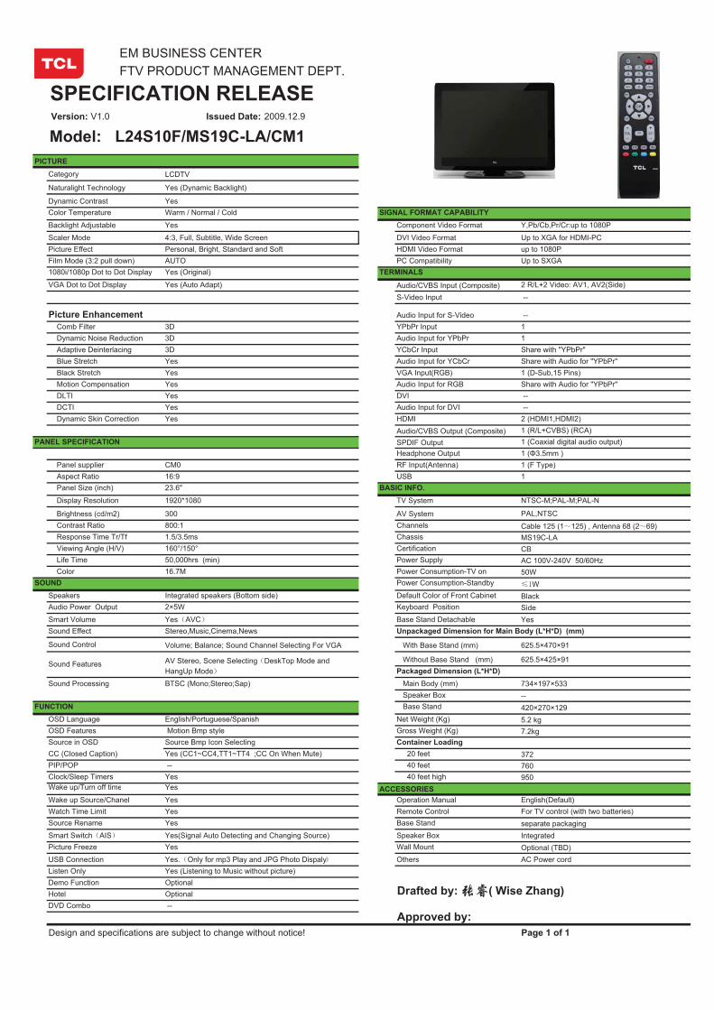
Dynamic Contrast YesColor Temperature Warm / Normal / Cold SIGNAL FORMAT CAPABILITYBacklight Adjustable Yes Component Video Format Y,Pb/Cb,Pr/Cr:up to 1080P
Scaler Mode 4:3, Full, Subtitle, Wide Screen DVI Video Format Up to XGA for HDMI-PCPicture Effect Personal, Bright, Standard and Soft HDMI Video Format up to 1080PFilm Mode (3:2 pull down) AUTO PC Compatibility Up to SXGA1080i/1080p Dot to Dot Display Yes (Original) TERMINALSVGA Dot to Dot Display Yes (Auto Adapt) Audio/CVBS Input (Composite) 2 R/L+2 Video: AV1, AV2(Side)
S-Video Input --
Audio Input for S-Video -- Comb Filter 3D YPbPr Input 1 Dynamic Noise Reduction 3D Audio Input for YPbPr 1 Adaptive Deinterlacing 3D YCbCr Input Share with "YPbPr" Blue Stretch Yes Audio Input for YCbCr Share with Audio for "YPbPr" Black Stretch Yes VGA Input(RGB) 1 (D-Sub,15 Pins) Motion Compensation Yes Audio Input for RGB Share with Audio for "YPbPr" DLTI Yes DVI -- DCTI Yes Audio Input for DVI -- Dynamic Skin Correction Yes HDMI 2 (HDMI1,HDMI2)
Headphone Output 1 (�3.5mm ) Panel supplier CM0 RF Input(Antenna) 1 (F Type) Aspect Ratio 16:9 USB 1 Panel Size (inch) 23.6" BASIC INFO. Display Resolution 1920*1080 TV System NTSC-M;PAL-M;PAL-N
Brightness (cd/m2) 300 AV System PAL,NTSC Contrast Ratio 800:1 Channels Cable 125 (1 125) , Antenna 68 (2 69) Response Time Tr/Tf 1.5/3.5ms Chassis MS19C-LA Viewing Angle (H/V) 160°/150° Certification CB Life Time 50,000hrs (min) Power Supply AC 100V-240V 50/60Hz Color 16.7M Power Consumption-TV on 50W
SOUND Power Consumption-Standby WSpeakers Integrated speakers (Bottom side) Default Color of Front Cabinet BlackAudio Power Output 2×5W Keyboard Position SideSmart Volume Yes AVC Base Stand Detachable YesSound Effect Stereo,Music,Cinema,News Unpackaged Dimension for Main Body (L*H*D) (mm)
Sound Control Volume; Balance; Sound Channel Selecting For VGA With Base Stand (mm) 625.5×470×91
Without Base Stand (mm) 625.5×425×91Packaged Dimension (L*H*D)
Sound Processing BTSC (Mono;Stereo;Sap) Main Body (mm) 734×197×533 Speaker Box --
FUNCTION Base Stand 420×270×129OSD Language English/Portuguese/Spanish Net Weight (Kg) 5.2 kgOSD Features Motion Bmp style Gross Weight (Kg) 7.2kgSource in OSD Source Bmp Icon Selecting Container LoadingCC (Closed Caption) Yes (CC1~CC4,TT1~TT4 ;CC On When Mute) 20 feet 372PIP/POP -- 40 feet 760Clock/Sleep Timers Yes 40 feet high 950Wake up/Turn off time Yes ACCESSORIESWake up Source/Chanel Yes Operation Manual English(Default)Watch Time Limit Yes Remote Control For TV control (with two batteries)Source Rename Yes Base Stand separate packagingSmart Switch AIS Yes(Signal Auto Detecting and Changing Source) Speaker Box IntegratedPicture Freeze Yes Wall Mount Optional (TBD)USB Connection Yes. Only for mp3 Play and JPG Photo Dispaly Others AC Power cordListen Only Yes (Listening to Music without picture) Demo Function OptionalHotel OptionalDVD Combo --
Design and specifications are subject to change without notice! Page 1 of 1
Model: L24S10F/MS19C-LA/CM1
Approved by:
AV Stereo, Scene Selecting DeskTop Mode andHangUp Mode
Picture Enhancement
Sound Features
Drafted by: ( Wise Zhang)
TCL Multimedia Technology Holdings Ltd. R&D Center
Alignment Procedure
MS19C-AP / MS19C-LA Chassis
Version: 1.0
Release Date: 2009-12-18
PREPARED BY: Wise Zhang DATE: 2009-12-18
APPROVED BY: DATE:
MS19C-AP/MS19C-LA
PRELIMINARY INFORMATION ----- SUBJECT TO CHANGE 2
Content1. General Description 3
2. Factory Menu 3
2.1 Way of accessing 3
2.2 Factory Menu 3
2.3 ADC calibration menu 5
2.4 White Balance adjustment 6
3. Design Menu 7
3.1 way of accessing 7
3.2 SHOP MENU 8
3.3 SERVICE MENU 9
3.4 PROJECT ID 10
3.5 PARAMETER SETTING MENU 10
3.6 HOTEL MENU 11
4. Steps of debugging 12
4.1 Device 12
4.2 steps of debugging 12
4.3 ADC calibration 12
4.4 White Balance adjustment 13
4.5 White Balance adjustment (automatically) 14
5. Chip list of software programming before SMT 14
6. USB software upgrade 15
History Description of major changes Release Date
V1.0 2009-12-18
Chassis Model
MS19C-AP L24P10F, L24S10F, L24V10F, L42M9F, L42N9F etc. FHD
MS19C-LA L24P10F, L24S10F, L24V10F etc.
HD MS19C-AP L26M9, L26N9, L32M9, L32N9 etc.
MS19C-AP/MS19C-LA
PRELIMINARY INFORMATION ----- SUBJECT TO CHANGE 3
2.2 Factory Menu
1. General Description MS19C-AP/MS19C-LA is our latest design especially for LCDTV products selling in Asia Pacific (AP) / Latin America (LA) market. It features by its high integration, easy debugging as well as convenience in terms of maintenance. Fast software upgrade through USB disk facilitates both manufacture and after service. Meantime, a variety of functions involved in Factory Menu (FM) and Design Menu (DM) can not only bring benefits for production, but also satisfy various demands of customer.
2.1 Accessing way: a. In the first place, press Menu button of remote control, then select Contrast item of Picture submenu. Finally, press 9, 7, 3, 5 consecutively.
b. When the FAC HOTKEY item of Factory Menu is enabled(ON), press Go Back button of remote control.
Factory Menu
Name Default Description Status
FAC HOTKEY
OFF Factory Menu shortcut button switch
The item must be disabled (OFF) after production
OK
WARM UP
OFF OFF: Normal mode. Display black screen when no signal. Turn to automatically standby mode if keep the signal unavailable over 15 minutes.
ON: Aging mode. Display snow dot when no signal. The set will not turn to standby even if the unavailability of signal
OK
ADC >> ADC calibration ( see details below) OK
WHITEBALANCE
>> White Balance Adjustment ( see details below) OK
SHOP DO It is crucial that the function is executed after production aim to clear information of production process, ensure user cannot access to Factory Menu after execute the item.
OK
NVM RESET DO Restore default value except WB and ADC data. OK
2. Factory Menu
MS19C-AP/MS19C-LA
PRELIMINARY INFORMATION ----- SUBJECT TO CHANGE 4
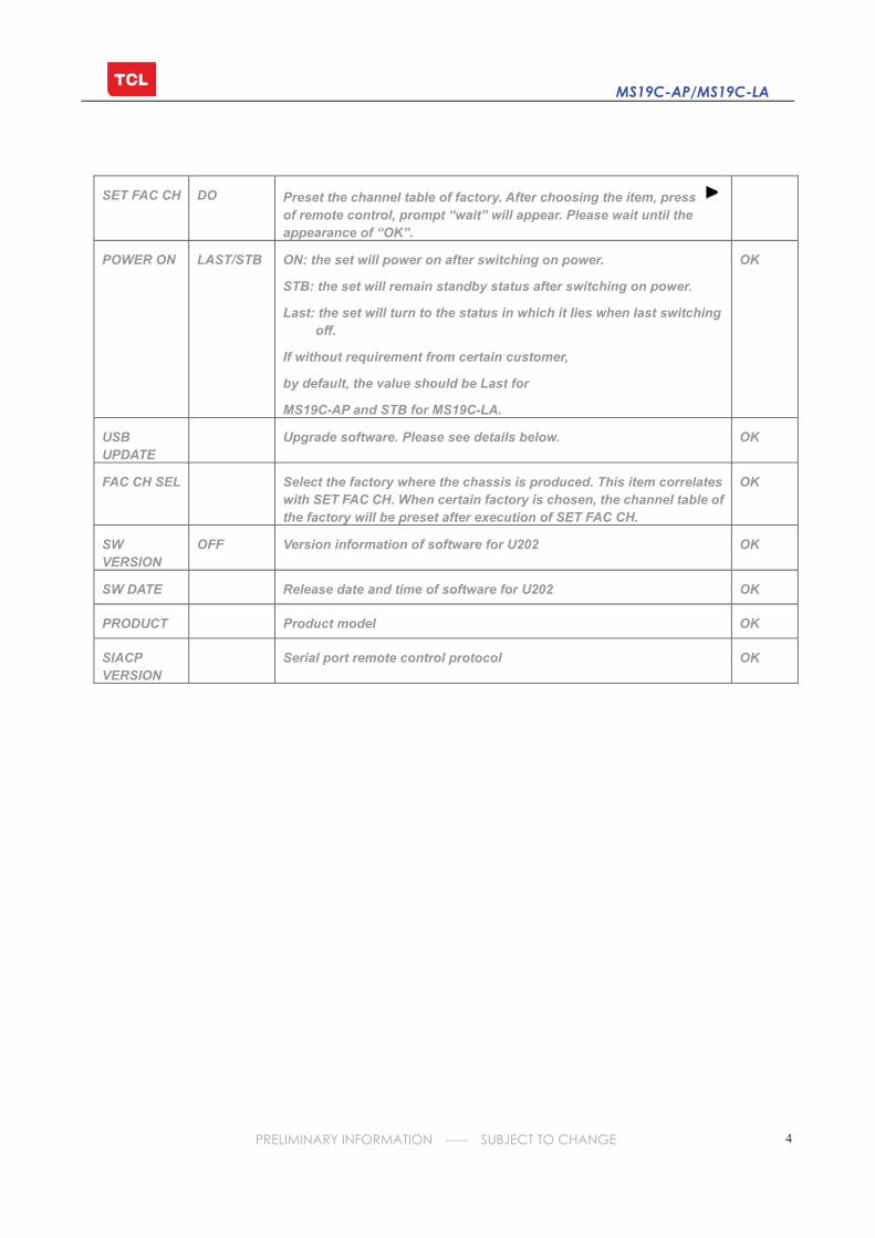
SET FAC CH DO Preset the channel table of factory. After choosing the item, press of remote control, prompt “wait” will appear. Please wait until the appearance of “OK”.
POWER ON LAST/STB ON: the set will power on after switching on power.
STB: the set will remain standby status after switching on power.
Last: the set will turn to the status in which it lies when last switching off.
If without requirement from certain customer,
by default, the value should be Last for
MS19C-AP and STB for MS19C-LA.
OK
USBUPDATE
Upgrade software. Please see details below. OK
FAC CH SEL Select the factory where the chassis is produced. This item correlates with SET FAC CH. When certain factory is chosen, the channel table of the factory will be preset after execution of SET FAC CH.
OK
SWVERSION
OFF Version information of software for U202 OK
SW DATE Release date and time of software for U202 OK
PRODUCT Product model OK
SIACP VERSION
Serial port remote control protocol OK
MS19C-AP/MS19C-LA
PRELIMINARY INFORMATION ----- SUBJECT TO CHANGE 5
2.3 ADC calibration menu ADC Menu Press the button in remote control to select certain item and
to change the value of ADC data or start ADC calibration.
Notes:
1. Only YPBPR and PC source should be calibrated.
ADC Calibration menu
Name Default Description Status
SOURCE Select the source you intend to ADC Calibrate.
Only YPBPR and PC are available.
OK
AUTO TUNE
DO Select and execute the item, ADC Calibration starts. It indicates a successful calibration if prompt “OK” is displayed. Otherwise, It is a failing calibration (“NG” displayed).
OK
R OFFSET 127 Offset of R channel ( cannot be changed after auto calibration) OK
G OFFSET 127 Offset of G channel ( cannot be changed after auto calibration) OK
B OFFSET 127 Offset of B channel ( cannot be changed after auto calibration) OK
R GAIN 128 Gain of R channel ( cannot be changed after auto calibration) OK
G GAIN 128 Gain of G channel ( cannot be changed after auto calibration) OK
B GAIN 128 Gain of B channel ( cannot be changed after auto calibration) OK
MS19C-AP/MS19C-LA
PRELIMINARY INFORMATION ----- SUBJECT TO CHANGE 6
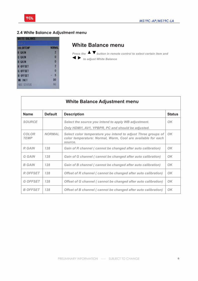
2.4 White Balance Adjustment menu
White Balance menu Press the button in remote control to select certain item and
to adjust White Balance
White Balance Adjustment menu
Name Default Description Status
SOURCE Select the source you intend to apply WB adjustment.
Only HDMI1, AV1, YPBPR, PC and should be adjusted.
OK
COLOR TEMP
NORMAL Select color temperature you intend to adjust Three groups of color temperature: Normal, Warm, Cool are available for each source.
OK
R GAIN 128 Gain of R channel ( cannot be changed after auto calibration) OK
G GAIN 128 Gain of G channel ( cannot be changed after auto calibration) OK
B GAIN 128 Gain of B channel ( cannot be changed after auto calibration) OK
R OFFSET 128 Offset of R channel ( cannot be changed after auto calibration) OK
G OFFSET 128 Offset of G channel ( cannot be changed after auto calibration) OK
B OFFSET 128 Offset of B channel ( cannot be changed after auto calibration) OK
MS19C-AP/MS19C-LA
PRELIMINARY INFORMATION ----- SUBJECT TO CHANGE 7
3 Design Menu
Design Menu
Name Default Description Status
DESIGNHOTKEY
OFF Design Menu shortcut button switch
The item must be disabled (OFF) after production
OK
FACTORY
MENU
>>> Access to Factory Menu OK
SHOP INIT >>> Contain many options which can be chosen according to the requirements of customers as default settings when leave factory.
See details below.
OK
OTHER >>> The item includes a number of functions offering convenience for R&D engineer to solve problems. It is exclusively used by R&D.
OK
SERVICE MENU
>>> Provide many useful information for after service
Please reference to SERVICE MENU submenu
OK
PARAM SETTING
>>> Include volume, brightness, contrast, saturation, sharpness, SSC setting. Please reference to PARAM SETTING submenu.
OK
HOTEL MENU
>>> Include special functions which bring benefits to hotel management. The item is accessible only when HOTELENABLE item is enabled (ON).
OK
3.1 Accessing way: 1. In the first place, press Menu button of remote control, then select Contrast item of Picture submenu. Finally, press 1, 9, 5, 0 consecutively.
2. When the DESIGN HOTKEY item of Design Menu isenabled (ON), press Go Back button of remote control.
Press the button in remote control to select certain item and to toggle among or execute the available options.
MS19C-AP/MS19C-LA
PRELIMINARY INFORMATION ----- SUBJECT TO CHANGE 8
3.2 SHOP MENU
SHOP MENU
Name Default Description Status
VOLUME 30 Volume setting, 0~100 adjustable OK
PIC MODE STANDARD Picture mode. Options:
STANDARD, BRIGHT, SOFT, USER.
OK
SOUNDMODE
STEREO Sound effects. Options:
STEREO, ODEUM, CINEMA, NEWS, USER.
OK
CH NUMBER 199 The maximum number of channel OK
LANGUAGE ENGLISH OSD language.
MS19C-AP
MS19C-LA English, Portuguese, Spanish
OK
COLOR SYS AUTO COLOR SYSTEM. Options: AUTO, PAL, NTSC, SECAM
PAL M, PAL N, NTSC4.43
OK
SOUND SYS M SOUND SYSTEM. Options:
MS19C-AP AUTO B/G, D/K, I, M
MS19C-LA AUTO
OK
PRESET CH 1 Preset channel. 0~199 optional OK
COLORTEMP
NORMAL Color temperature. Option: NORMAL, WARM, COOL OK
Contain many options which can be chosen according to the
requirements of customers as default settings when leave factory.
Press the button in remote control to select certain item and
to toggle among the available options..
MS19C-AP/MS19C-LA
PRELIMINARY INFORMATION ----- SUBJECT TO CHANGE 9
3.3 SERVICE MENU
Press the button in remote control to select certain item and
to toggle among the available options..
SERVICE MENU (PRODUCT INFO)
Name Default Description Status
SWVERSION
Software virtual code No. OK
DATE, TIME Release date, time OK
PRODUCT Model of product OK
SIACP VERSION
Serial port remote control protocol OK
CHASSIS MS19C-AP/MS19C/LA Chassis name OK
PANEL Panel code OK
ERROR CODE
NG
USBUPDATE
USB upgrade. Reference to descript below. OK
PROJECT ID
Select project parameters through project ID. OK
TCL SHOW OFF Switch of DEMO function. It is designed for demo in shop and must be closed after selling out.
OK
HOTEL ENABLE
OFF Switch of Hotel Menu. OK
LOGOSELECT
ON Choose LOGO according to customer demand OK
AV OVERSCANCAL
>>> OVERSCAN adjustment OK
MS19C-AP/MS19C-LA
PRELIMINARY INFORMATION ----- SUBJECT TO CHANGE 10
3.4 PROJECT ID
3.5 PARAM SETTING MENU
PARAM SETTING MENU
Name Default Description Status
VOLUME >>> Sound curve. Exclusively used by R&D. OK
BRIGHTNESS >>> Brightness curve. Exclusively used by R&D. OK
CONTRAST >>> Contrast curve. Exclusively used by R&D. OK
SATURATION >>> Saturation curve. Exclusively used by R&D. OK
SHARPNESS >>> Sharpness curve. Exclusively used by R&D. OK
SSCSETTING
>>> SSC parameters. Exclusively used by R&D. OK
Press the button in remote control to select certain item and
to enter menu.
PROJECT ID number Product model
Remote control name
Power supply number Panel code
MS19C-AP/MS19C-LA
PRELIMINARY INFORMATION ----- SUBJECT TO CHANGE 11
3.6 HOTEL MENU
Press the button in remote control to select certain item and
to enter submenu.
HOTEL MENU
Name Default Description Status
POWERLOGO
ON LOGO select OK
CH LOCK OFF Channel scan lock. OK
MAX VOL 100 Max volume OK
AUTO SET OFF The switch of PIC MODE, SOUND MODE etc.
When it is ON, these items are selectable.
OK
PIC MODE STANDARD Picture mode. OK
SOUND MODE
STEREO Sound mode OK
POWERVOL.
50 Default volume when power on OK
POWERSIGNAL
TV Default signal source when power on OK
POWERCHANNEL
1/2 Default channel no. when power on OK
KEY LOCK OFF Lock the keys. OK
SAVE DATA TO USB
DO Save the settings of Hotel Menu to USB OK
WRITEDATA FROM USB
DO Copy the settings of Hotel Menu from USB OK
MS19C-AP/MS19C-LA
PRELIMINARY INFORMATION ----- SUBJECT TO CHANGE 12
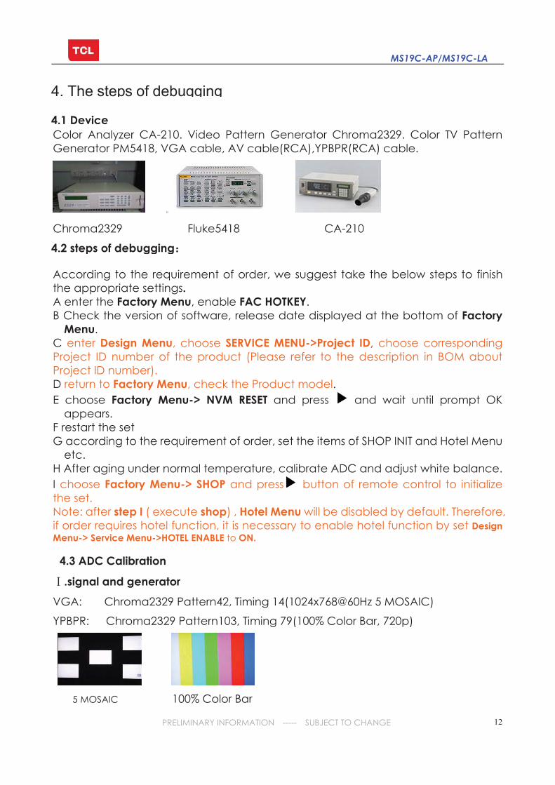
Color Analyzer CA-210. Video Pattern Generator Chroma2329. Color TV Pattern Generator PM5418, VGA cable, AV cable(RCA),YPBPR(RCA) cable.
Chroma2329 Fluke5418 CA-210
According to the requirement of order, we suggest take the below steps to finish the appropriate settings.A enter the Factory Menu, enable FAC HOTKEY.B Check the version of software, release date displayed at the bottom of Factory
Menu.C enter Design Menu, choose SERVICE MENU->Project ID, choose corresponding Project ID number of the product (Please refer to the description in BOM about Project ID number).D return to Factory Menu, check the Product model.E choose Factory Menu-> NVM RESET and press and wait until prompt OK
appears.F restart the set G according to the requirement of order, set the items of SHOP INIT and Hotel Menu
etc. H After aging under normal temperature, calibrate ADC and adjust white balance. I choose Factory Menu-> SHOP and press button of remote control to initialize the set.Note: after step I ( execute shop) , Hotel Menu will be disabled by default. Therefore, if order requires hotel function, it is necessary to enable hotel function by set DesignMenu-> Service Menu->HOTEL ENABLE to ON.
YPBPR: Chroma2329 Pattern103, Timing 79(100% Color Bar, 720p)
5 MOSAIC 100% Color Bar
4. The steps of debugging
4.1 Device
4.2 steps of debugging
4.3 ADC Calibration
MS19C-AP/MS19C-LA
PRELIMINARY INFORMATION ----- SUBJECT TO CHANGE 13
.steps of debug:
1) Access to the Factory menu->ADC
2) Select PC source
3) Select AUTO TUNE Press button in your remote control to calibrate the ADC automatically.
4) Select YPBPR source
5) Repeat step 3.
6) When the OK appears the calibration has been finished successfully.
VGA calibration YPBPR calibration
Before adjustment, you must ensure Color Analyzer has been calibrated. Only AV1, YPBPR, VGA , HDMI 1 need to be adjusted. It is necessary to adjustment HDMI 1 firstly.
a. signal and generator The pattern of the signal should be used are White (Chroma2329 pattern113) and Grey (pattern 114).The format of signal are respectively 720p for HDMI1 (Chroma2329 Timing 69), NTSC for AV1 (Chroma2329 Timing 37),1024×768@60Hz
(Chroma2329 Timing 14) for VGA and 720p (Chroma2329 Timing 79)for YPBPR
b. steps of adjustment 1) enter the factory menu-> White Balance, select source HDMI 1 and COLORTEMPnormal.2) input grey signal in 720p format
3) change R OFFSET and B OFFSET to make sure the value of color coordination equal to (x=280+/-5,y=290+/-5).
4) input white signal in 720p format
4.4 White Balance adjustment (Manual)
MS19C-AP/MS19C-LA
PRELIMINARY INFORMATION ----- SUBJECT TO CHANGE 14
5) change R Gain and B Gain to make sure the value of color coordination equal to
(x=280+/-5,y=290+/-5).
6) repeat step 2~5 until both of the value of color coordination of white and grey
equal to (x=280+/-5,y=290+/-5).
In addition to select COLORTEMP COOL/WARM, the adjustment method of COOLand WARM color temperature is same with that of NORMAL. The color coordination we recommend for COOL and WARM color temperature is respectively (270+/-5, 270+/-5) and (300+/-5, 305+/-5). Except select corresponding SOURCE and signal, the method of white balance adjustment for AV1, VGA and YPBPR is same with that of HDMI 1.
4.5 ADC Calibration and White Balance Adjustment (automatic)The process of adjusting ADC and White Balance automatically is out of the range of this file. Please refer to the relevant technical file of HuiZhou factory of TCL
5. Chip list of software programming before SMT Following chips must be programmed before SMT by ALL-11 or other tools.
Note: 1) the software for U202( Flash software) and U203 (HDCP) of Main Board can be
program using ISP tool. 2) Please check HDCP function in the process of production. 3) EDID of VGA and HDMI source are integrated in the software for U202,
therefore, there is no need to program extra EDID software for MS19C-AP/LA chassis.
Position Chip type Software description
1 U202 Flash main software
2 U203 E2PROM HDMI HDCP key
HDMI White Balance adjustment
MS19C-AP/MS19C-LA
PRELIMINARY INFORMATION ----- SUBJECT TO CHANGE 15
6. Software upgrade through USB disk
Way 1: 1) Please ensure the software you are using has a correct file name
(if the resolution of panel is 1920*1080, the software name should
be TCL_MS19C_UPDATE_FHD.bin, if resolution is 1366*768, file name
should be TCL_MS19C_UPDATE.bin, copy it to the root directory of a
USB disk.
2) Insert the USB disk to the USB socket of the set for which you are
going to upgrade program.
3) Enter the Factory Menu, select USB UPDATE, press button of
remote control to start upgrade.
Way 2: 1) Please ensure the software you are using has a correct file name
(if the resolution of panel is 1920*1080, the software name should
be TCL_MS19C_UPDATE_FHD.bin, if resolution is 1366*768, file name
should be TCL_MS19C_UPDATE.bin, copy it to the root
directory of a USB disk.
2) Insert the USB disk to the USB socket of the set for which you are going
to upgrade program.
press CH- button in key board and switch on at the same time. Wait
for 10 seconds then let off the CH- button to start upgrade
Notes:
We recommend you use former way to
upgrade if the set can work properly.
In some circumstances, such as no
picture, however, the set cannot be
upgraded successfully by means of
the former way, the later way can
be an alternative. Over the course of
upgrade, power supply cannot be cut off. Otherwise, to upgrade program, it is necessary to adopt ISP tool. After
upgrading the software, please restart the set (power off then power on) in
order to ensure the correct EEPROM data. Left figure shows the prompt
after upgrade.
MS1
9C (A
P&LA
) Cha
ssis
Blo
ck D
iagr
am
12V
or 5
V
LVD
S_S
EL
BL_ON
DIM
24V
Firs
t Iss
ued
V
0.1
ZC
X 2
009-
12-0
6
LCD
Pan
el
U20
1
Mai
nch
ipse
t
Z101
TUN
ER
CN
&A
P07
-380
FI5-
NA
9GLA
07-4
57FF
5-N
A2G
U60
113
-STA
559-
BW
B(2
4~37
")13
-STA
335-
BW
B(4
0~52
")
U60
213
-RC
4558
-DR
B
8R/8
W
P50
3:47
-RC
A28
6-X
X0G
P40
1:47
-HD
I008
-XS
1
P40
3:47
-VG
A01
9-X
X0
U80
3D
C/D
C13
-MP
1593
-C2B
Pow
er B
oard
M
odul
e
PW
L323
5-01
IPB
:IP
L192
2LIP
L22C
LPL2
4CIP
L42A
-01
X10
1S
AW
F (P
ictu
re)
CN
&AP
: 45-
SA
WK
62-7
4DLA
: 45-
SA
WF3
9-53
0
X10
2S
AW
F (S
ound
)C
N&
AP
: 45-
SA
WK
93-5
2MLA
: 45-
SA
WF9
3-70
0
PC
INP
UT
R/G
/B/H
S/V
S
AV
1 IN
PU
TV
ideo
P50
2:47
-RC
A24
9-X
X2G
AV
2 IN
PU
TV
ideo
HD
MI 2
IN
PU
T
U50
2A
udio
SW
13-E
F405
2-B
TB
TV V
TV SIF
Tune
r I2
C B
US
AM
P L
/R
P50
4:47
-RC
A275
-XX
0G
VID
EO
OU
TPU
T V
/ L/R
SP
DIF
OU
TPU
T
LVD
S O
dd S
igna
l
U20
2FL
AS
H M
EM
OR
YC
N&
AP
13-W
25X
32-V
SB
LA13
-W25
Q16
-00B
U20
4E
EPR
OM
13-M
24C
64-W
6B
U20
3H
DC
P K
EY
13-M
24C
04-M
NB
SP
I BU
S
I2C
BU
S
AC
U80
7D
C/D
C13
-RT8
110-
00B
U80
1LD
O13
-AZ1
084-
33B
U10
2LD
O13
-AS
1117
-50B
+12V
+5V
U81
1LD
O13
-AZ1
117-
DA
B
U80
8M
OS
FET
12-1
3N03
L-0B
X
For t
uner
& IF
de
mod
ulat
or+5
V_I
F
For A
udio
Am
plifi
er P
ower
+12V
_AM
P
24/1
2V-S
W
STB
_CTL
1V
26
PW_ON/OFF
STB_CTL
AMP-MUTE
PANEL_ON/OFF
BL_PWM
HDMI_DET
LED
WP_EEP
AU SW0/SW1
IR_SYNC
RESET
RXD/TXD
3V3STB/1V26/+3.3V
Not
e: If
use
inne
r dem
odul
atio
n,th
is p
art N
C.
Pow
er S
uppl
y B
lock
Dia
gram
KEY1/KEY2
D80
4
P40
2:47
-HD
I008
-XS
1
HD
MI 1
IN
PU
T
U60
313
-TD
A151
-7A
B(1
9~22
")
U20
5D
DR
SD
RA
M13
-W94
12G
-61BU50
113
-RC
4558
-DR
BA
UD
IO O
UTP
UT
Q10
3IF
AM
P11
-SC
3779
-DBX
I2S
BU
S
Ear
phon
e L
/R
P50
1:47
-RC
A25
5-X
X0G
YP
BP
R I
NP
UT
Vid
eo
P50
5:47
-RC
A27
6-X
X0G
US
B I
NP
UT
MU
X L
/RAU
SW
0
AU S
W1
Y0
Y1
Y3
Y2
U10
1
IFde
mod
ulat
or
13-T
DA
988-
5TB
S
V_IF
S_IF
VID
EO
OU
TPU
T
AU
DIO
AM
P
LVD
S E
ven
Sig
nal
DC
24V
DC
12V
3V3S
TB
5VS
TB/D
C 5
V
U81
0LD
O13
-LD
1117
-DTB
Q80
8Q
810
D80
3
D81
4D
808
U80
4LD
O13
-AS1
117-
25B
+24V
_AM
P
U60
3:13
-TD
A15
1-7A
B(1
9~22
")U
601:
13-S
TA55
9-B
WB
(24~
37")
U60
1:13
-STA
335-
BW
B(4
0~52
")
+3.3
V
DC
12V
5VA
IN
U80
5D
C/D
C13
-MP
1482
-DS
B
+2_6
VFo
r DD
R
D81
7
5VS
TB/D
C 5
V
3V3S
TB
3V3S
TBD
C 2
4V
+3_3
VS
TB
1V
26
Not
e: If
use
U81
1,th
is p
art N
C.
PW
_ON
/OFF
P40
4:47
-US
B00
2-X
X0
P604
:47-
EAR
005-
XX
0
S_I
F
V_I
F
MONO
DG
ND
T
T
DG
ND
DG
ND
DG
ND
DG
ND
DG
ND
DG
ND
DG
ND
DG
ND
DG
ND
DG
ND
DG
ND
DG
ND
DG
ND
DG
ND
DG
ND
OUT2
OUT1
GND
IN/GND
IN
DG
ND
DG
ND
DG
ND
DG
ND
DG
ND
DG
ND
DG
ND
DG
ND
DG
ND
DG
ND
A
1
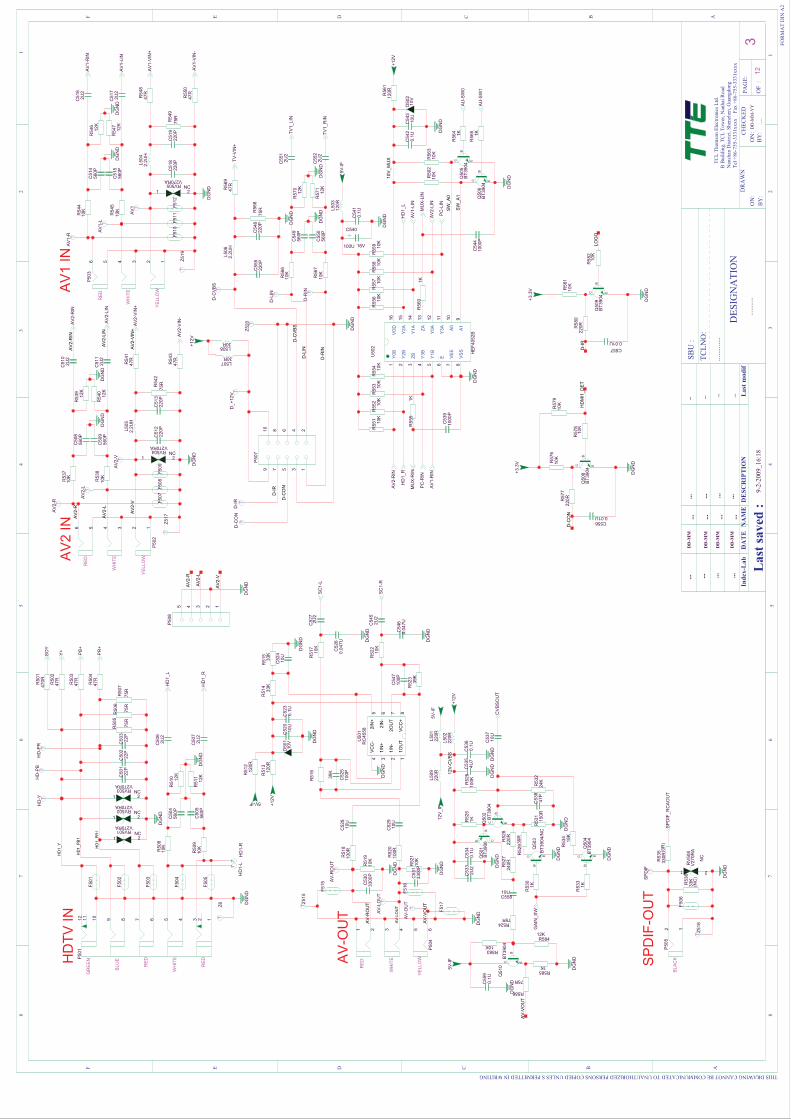
F E D C B
87
65
43
21
THIS DRAWING CANNOT BE COMMUNICATED TO UNAUTHORIZED PERSONS COPIED UNLES S PERMITTED IN WRITING