December 6, 2017 © 2017 Transphorm Inc. Subject to change without notice.
User Guide
TDHBG2500P100: 2.5kW Half-bridge Evaluation Board
Introduction The TDHBG2500P100 half-bridge evaluation board provides the elements of a simple buck or boost converter for basic study of
switching characteristics and efficiency achievable with Transphorm’s 650V GaN FETs. In either buck or boost mode the circuit
can be configured for synchronous rectification. Jumpers allow use of a single logic input or separate hi/lo inputs. The high-
voltage input and output can operate at up to 400Vdc, with a power output of up to 2.5kW. The inductor provided is intended for
efficient operation at 100kHz, although other inductors and other frequencies may be easily used.
The TDHBG2500P100-KIT is for evaluation purposes only.
Figure 1. TDHBG2500P100 half-bridge evaluation board
TDHBG2500P100_0v6 December 6, 2017
TDHBG2500P100 User Guide
Warnings
TDHGB2500P100 input/output specifications
High-voltage input/output: 400Vdc max
Auxiliary supply (J1): 10V min, 18V max
Logic inputs: nominal 0V-5V
Pulse-generation circuit: Vlo < 1.5V, Vhi > 3.0V
Direct connection to gate driver: Vlo < 0.8V, Vhi > 2.0V
SMA coaxial connectors
Switching frequency: configuration-dependent
Lower limit determined by peak inductor current
Upper limit determined by desired dead-time and power dissipation
Power dissipation in the GaN FET is limited by the maximum junction temperature. Refer to the TPH3212PS datasheet.
Circuit description The circuit comprises a simple half-bridge featuring two TPH3212PS GaN FETs, as indicated in the block diagram of Figure 2.
Two high-voltage ports are provided which can serve as either input or output, depending on the configuration—boost or buck. In
either case one FET acts as the active power switch while the other carries the freewheeling current. The latter device may be
enhanced, as a synchronous rectifier, or not. With GaN FETs the reverse recovery charge is low and there is no need for
additional freewheeling diodes. Two input connectors are provided which can be connected to sources of logic-level command
signals for the hi/lo gate driver. Both inputs may be driven by off-board signal sources; or alternatively, a single signal source
may be connected to an on-board pulse-generator circuit which generates the two non-overlapping pulses. Jumpers determine
how the input signals are used.
An inductor is provided as a starting point for investigation. This is a 440µH toroid intended to demonstrate a reasonable
compromise between size and efficiency for power up to 2.5kW at a switching frequency of 100kHz.
TDHBG2500P100_0v6 December 6, 2017
TDHBG2500P100 User Guide
Figure 2. Functional block diagram
Using the board The board can be used for evaluation of basic switching functionality in a variety of circuit configurations. It is not a complete
circuit, but rather a building block. It can be used in steady-state DC/DC converter mode with output power up to 2.5kW.
When operating the board at high power (>1000W), an external fan should be used to cool the heatsink.
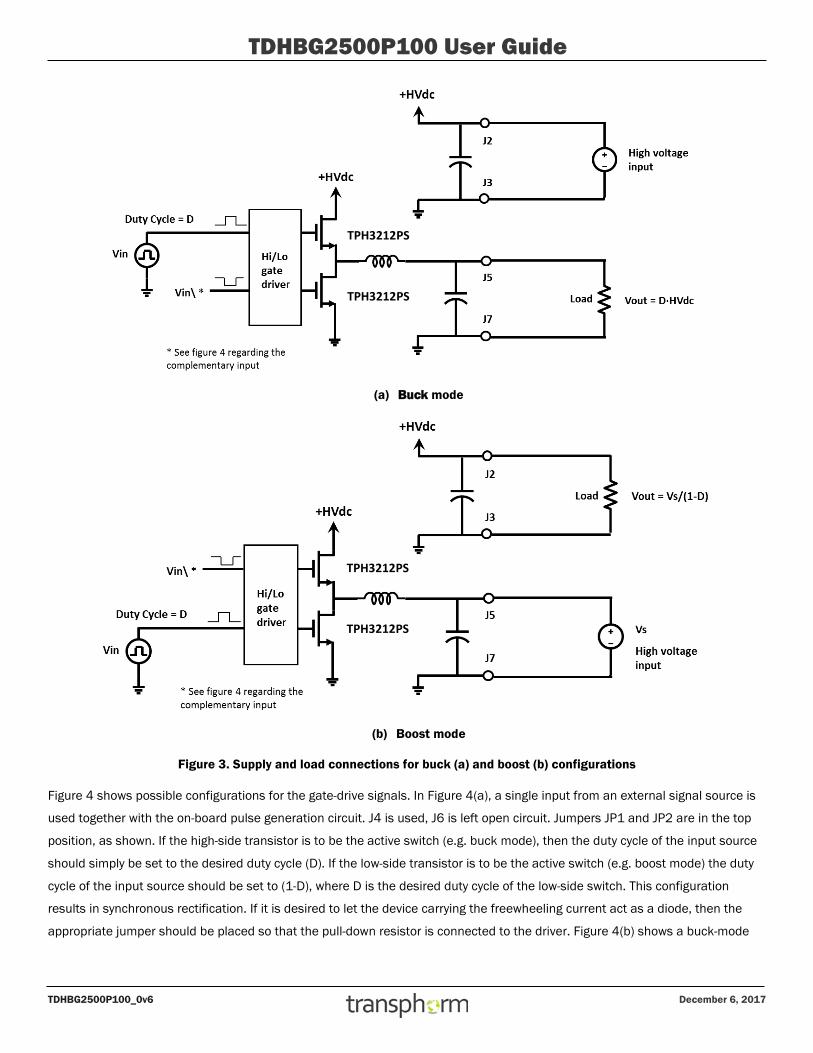
Configurations Figure 3 shows the basic power connections for buck and boost modes. For buck mode, the HVdc input (terminals J2, J3) is
connected to the high-voltage supply and the output is taken from terminals J5 and J7. For boost mode, the connections are
reversed.
Note that in boost mode a load must be connected. The load current affects the output voltage up to the transition from DCM to
CCM. In buck mode the load may be an open circuit.
TPH3212PS
TPH3212PS
TDHBG2500P100_0v6 December 6, 2017
TDHBG2500P100 User Guide
(a) Buck mode
(b) Boost mode
Figure 3. Supply and load connections for buck (a) and boost (b) configurations
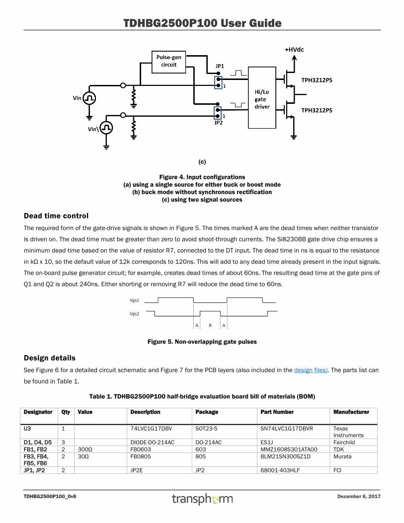
Figure 4 shows possible configurations for the gate-drive signals. In Figure 4(a), a single input from an external signal source is
used together with the on-board pulse generation circuit. J4 is used, J6 is left open circuit. Jumpers JP1 and JP2 are in the top
position, as shown. If the high-side transistor is to be the active switch (e.g. buck mode), then the duty cycle of the input source
should simply be set to the desired duty cycle (D). If the low-side transistor is to be the active switch (e.g. boost mode) the duty
cycle of the input source should be set to (1-D), where D is the desired duty cycle of the low-side switch. This configuration
results in synchronous rectification. If it is desired to let the device carrying the freewheeling current act as a diode, then the
appropriate jumper should be placed so that the pull-down resistor is connected to the driver. Figure 4(b) shows a buck-mode
TPH3212PS
TPH3212PS
TPH3212PS
TPH3212PS
TDHBG2500P100_0v6 December 6, 2017
TDHBG2500P100 User Guide
configuration where the low-side device is not enhanced. Finally, Figure 4(c) shows use of two external signal sources as inputs
to the gate driver.
For any configuration, an auxiliary supply voltage of 10V-18V must be supplied at connector J1.
Pull-down resistors R5 and R6 have a value of 4.99k. If a 50Ω signal source is used and 50Ω termination is desired, then R5
and R6 may be replaced (or paralleled) with 1206 size 50Ω resistors.
Boost mode/buck mode operation
For buck mode operation, with input voltage of 400V and output voltage of 48V; 50A max output current is achievable at
2500W with duty cycle of 12%. A typical 400Vin - 200Vout buck operation with 50% duty cycle, 6.5A max output current is seen
at 2500W. On the other hand, for 200Vin - 400Vout boost mode operation at 2.5kW, 12.5A max output current can be reached
with a duty cycle of 50%. Thermal cooling must be enforced for high current switching at all times.
(a)
(b)
TPH3212PS
TPH3212PS
TPH3212PS
TPH3212PS
TDHBG2500P100_0v6 December 6, 2017
TDHBG2500P100 User Guide
(c)
Figure 4. Input configurations (a) using a single source for either buck or boost mode
(b) buck mode without synchronous rectification (c) using two signal sources
Dead time control The required form of the gate-drive signals is shown in Figure 5. The times marked A are the dead times when neither transistor
is driven on. The dead time must be greater than zero to avoid shoot-through currents. The Si8230BB gate drive chip ensures a
minimum dead time based on the value of resistor R7, connected to the DT input. The dead time in ns is equal to the resistance
in kΩ x 10, so the default value of 12k corresponds to 120ns. This will add to any dead time already present in the input signals.
The on-board pulse generator circuit; for example, creates dead times of about 60ns. The resulting dead time at the gate pins of
Q1 and Q2 is about 240ns. Either shorting or removing R7 will reduce the dead time to 60ns.
Figure 5. Non-overlapping gate pulses
Design details See Figure 6 for a detailed circuit schematic and Figure 7 for the PCB layers (also included in the design files). The parts list can
be found in Table 1.
Table 1. TDHBG2500P100 half-bridge evaluation board bill of materials (BOM)
Designator Qty Value Description Package Part Number Manufacturer
U3 1 74LVC1G17DBV SOT23-5 SN74LVC1G17DBVR Texas Instruments
D1, D4, D5 3 DIODE-DO-214AC DO-214AC ES1J Fairchild FB1, FB2 2 300Ω FB0603 603 MMZ1608S301ATA00 TDK FB3, FB4, FB5, FB6
2 30Ω FB0805 805 BLM21SN300SZ1D Murata
JP1, JP2 2 JP2E JP2 68001-403HLF FCI
TPH3212PS
TPH3212PS
TDHBG2500P100_0v6 December 6, 2017
TDHBG2500P100 User Guide
Designator Qty Value Description Package Part Number Manufacturer
J2, J3, J5, J7
4 KEYSTONE_7691 KEYSTONE_7691 7691 Keystone
LED1, LED2, LED3
3 LEDCHIP-LED0805 CHIP-LED0805 SML-211UTT86 Rohm
U1 1 LT3082 SOT223-3 LT3082EST#PBF Linear Technology
J1 1 PJ-002AH PJ-002AH PJ-002AH CUI LDS, LGS 2 TEKTRONIX-PCB TEKTRONIX-PCB 131-4353-00 Tektronix C7 1 0.1µF C-EUC1812 C1812 C1812V104KDRACTU Kemet C10, C11, C12, C14, C20, C21, C22
7 0.1µF C-USC0603 C0603 06033C104JAT2A AVX
C8, C16, C17
3 0.1µF C-USC2225K C2225K VJ2225Y104KXGAT Vishay
R15 1 0Ω R-US_R0603 R0603 RC0603FR-070RL Yageo R16, R23 2 20Ω R-US_R1206 R1206 RNCP1206FTD20R0 Stackpole R9, R12 2 0Ω R-US_R1206 R1206 ERJ-8GEY0R00V Panasonic R4 1 10Ω R-US_R0805 R0805 ERJ-P06J100V Panasonic R14 1 100kΩ R-US_R0603 R0603 ESR03EZPJ104 Rohm C19, C23 2 100pF C-USC0603 C0603 06035A101FAT2A AVX R3 1 10MΩ R-US_R1206 R1206 HVC1206T1005JET Stackpole R7, R11 2 10kΩ R-US_R0603 R0603 ERJ-3GEYJ103V Panasonic C13, C15 2 10µF C-EUC0805 C0805 C0805C106M4PACTU Kemet R8, R10 2 1kΩ R-US_R0603 R0603 RC0603FR-071KL Yageo C2 1 1µF C-EUC0805 C0805 CC0805ZRY5V8BB105 Yageo C3 1 2.2µF C-EUC0805 C0805 C2012X5R1E225K125AC TDK C1 1 22µF C-USC1206 C1206 CL31A226MOCLNNC Samsung R13 1 2kΩ R-US_R0805 R0805 RC0805FR-072KL Yageo C4, C5, C6, C24
4 4.7nF C-EUC1206 C1206 C1206C472KDRACTU Kemet
R1, R5, R6 6 4.99kΩ R-US_R1206 R1206 RMCF1206FT4K99 Stackpole R17, R18, R19, R20, R21, R22
6 560kΩ R-US_R0805 R0805 ESR10EZPJ564 Rohm
R2 1 499kΩ R-US_R1206 R1206 RMCF1206FT499K Stackpole C9, C18 2 10µH 10uH EPCOS_B32674 B32794D2106K Epcos U4, U5 2 74AHC1G86DBV SOT23-5 SN74AHC1G86DBVR Texas
Instruments D2, D3 2 BAT54 SOT23 BAT54W NXP J4, J6 2 BU-SMA-G BU-SMA-G 5-1814832-1 TE Connectivity U$3 1 460µH Inductor CWS-1MP-12640 CWS HS1 1 HEATSINKC220-050-
2AE C220-050-2AE Ohmite
U2 1 SI8230 SOIC16N SI8230BB-D-IS SiLabs Q1, Q2 2 72mΩ TPH_TO220VERT_TRI TO-220 TPH3212PS Transphorm 2 Thermal pad between
TPH3212 and heatsink
SP2000-0.015-00-54 Bergquist
2 4-40 screw 9900 Keystone 2 Nylon washer shoulder 3049 Keystone 1 12V Adaptor TRG10R120-11E03-
Level-VI Cincon
4 Bumper cylin 0.312" dia blk
SJ61A1 3M
TDHBG2500P100_0v6 December 6, 2017
TDHBG2500P100 User Guide
Figure 6. Detailed circuit schematic
TDHBG2500P100_0v6 December 6, 2017
TDHBG2500P100 User Guide
(a) PCB top layer
(b) PCB bottom layer
TDHBG2500P100_0v6 December 6, 2017
TDHBG2500P100 User Guide
(c) PCB inner layer 2 (ground plane) + inner layer 3 (power plane)
Figure 7. PCB layers
Probing
Plated through-holes labeled test points (LGS and LDS) are provided for probing the low-side gate pulse and half-bridge
switching node waveform. In order to minimize inductance during measurement, the tip and the ground of the probe should be
directly attached to the sensing points to minimize the sensing loop. For safe, reliable and accurate measurement, a scope
probe tip may be directly soldered to the low-side FET drain and a short ground wire soldered to the low-side FET source. See
Figure 8 for an alternative that does not require soldering the probe tip.
WARNINGS:
There is no specific protection against over-current or over-voltage on this board.
If the on-board pulse generation circuit is used in boost mode, a zero input corresponds to 100% duty cycle for the active low-
side switch.
TDHBG2500P100_0v6 December 6, 2017
TDHBG2500P100 User Guide
Figure 8. Low-inductance probing of fast, high-voltage signals
Efficiency has been measured for this circuit in boost mode with 200Vdc in and 400Vdc out, switching at 50kHz and 100kHz
(Figure 9).
Figure 9. Efficiency for a boost 200V:400V converter