60
TDTS01 Computer Aided Design of Electronics Lab Compendium 2014.01.27-00

TDTS01
Computer Aided Design of Electronics
Lab Compendium 2014.01.27-00

TDTS01 - Computer Aided Design of Electronics 2
Authors history
2014, Nima Aghaee
2013, Nima Aghaee 2011, Adrian Lifa
2012, Nima Aghaee 2010, Zhiyuan He
Acknowledgments
The authors would like to thank Dimitar Nikolov for his contributions to chapters 6.
Table of Contents
TDTS01 1
Chapter 1 Lab Assignments 4
Chapter 2 Introduction 9
Chapter 3 Preparation for the Lab 12
3.1 Setting up the CAD Tool Environment 12
3.2 Setting up Environment Variables 13
3.3 Preparing Files for Tutorial 14
Chapter 4 Tutorial of Project Specification, Compilable Design, Testbench, and Simulation 15
4.1 Design Specification 15
4.2 Compiling the VHDL code 16
4.3 Simulation 20
4.3 Do file 23
Chapter 5 Tutorial of Synthesis 24
Chapter 6 Tutorial of Design for Testing 30
6.1 Automatic Test Pattern Generation 31
6.2 Automatic Scan Chain Insertion 33
Attachments Codes for the Example (1st assignment) 36

NOTE:
You need to read this document twice.
First, when you are doing the 1st assignment (Project specification and tool
set experience). In this first time, some parts of this document might be difficult to understand properly. Meanwhile you are learning new things because of the course lectures, your self-study, and also learning by doing the 1st assignment.
Second time is when you are doing your project. You should be able to understand this document properly and easily in the second time.
In either case, please do not hesitate to ask questions from the lab assistant.
Noticeable changes compared to the previous versions:
Section 6.2 is added to chapter 6.

TDTS01 - Computer Aided Design of Electronics 4
Chapter 1 Lab Assignments
Students are supposed to do their own projects by following the design and test flow that will be introduced in this document. Project topics can be picked from topics suggested in this document or can be suggested by students. Two students should work together in a team. There are four assignments. For an assignment a report should be delivered on/before its deadline and a demonstration by both group members should be done on/before assignment deadline. Please form groups of two and register for the lab on “webreg” as soon as possible. Assignments are as follows:
1. Project specification and tool set experience [deadline: 13-Feb]
o Describe the following in the report
Functional behavior
Timing behavior (in respect to hand-shaking signals)
Targeted design metric (area xor delay)
o Demonstrate the design flow using the provided example
o Mention noticeable experiences with the tool set in addition to the explicitly requested material in the report
2. Compilable design and testbench [deadline: 25-Feb]
o Successful simulation of the design (functional and timing)
3. Synthesizable design [deadline: 07-Mar]
o Successful simulation of the synthesizable design (functional and timing)
o Synthesis of the design to the gate level
o Description of the choices that you have made to help the targeted design metric
4. Manufacturing test [deadline: 14-Mar]
o Test pattern generation
o Improvement of testability. The following should be reflected in the report:
Obtaining the original testability statistics.
Analyzing the design from the testability point of view. Write a short discussion in the report. The analysis could be rather qualitative than quantitative.
Modify the design in order to improve the testability. Mention the changes you have made, in the report. Make sure that you save the original design and the modified design separately. During the demonstrations you might be asked to work with both of them.
Repeat the design flow in order to obtain the new testability statistics. Repeat this procedure until you are satisfied with the results.
The order of the assignments matters since they are dependent. Please do not invest much time on the next assignment when the previous one is not passed.
All assignments are required to be completed.

TDTS01 - Computer Aided Design of Electronics 5
Please fill in the feedback forms (at the end of this document) for every assignment and deliver them.
Improvement of the testability is a necessary part. The important thing here is a convincing argument about the analysis of the design and the modifications, and describing how they help to improve the testability. The amount of improvement per se is not crucial.
Please include the items that are asked for in the following chapters in your report. Do not forget to email your source codes (items similar to section 3.3)
Please do not attach the complete source codes to the report (save paper and print). However they should be sent as attachments to an email.
o The parts of the code that you are explaining should appear within the report.
Please keep the following files separately to the very end (until your final mark is registered):
o Report for project specification and tool-set experience
o Compilable design
o Testbench
o Report for compilable design and testbench
o Synthesizable design
o Report for synthesizable design
o Synthesizable design after final testability improvement
o Report for manufacturing test
In case your compilable design is also synthesizable, it is fine to use it as the synthesizable design. But a convincing argument on the design choices you have made in favor of the targeted design metric is crucial.
o A design is compilable if it compiles and simulates (vcom and vsim commands in ModelSim). See chapter 4.
o A design is synthesizable if the LeonardoSpectrum could generate the output netlist (*.v) file (See chapter 5). There are two situations that a design is not synthesizable:
In theory, using the selected semiconductor technology, it is not possible to make a circuit for that HDL code. In this case the question to the designer is: Do you really need all the details that you specified in your code to achieve the required functionality? Try to remove the unnecessary details. Examples might be double edge clocks or multiple clocks.
The synthesis tool is not able to synthesize the code, however in theory it is possible to synthesize it. Synthesis is, in fact, adding

TDTS01 - Computer Aided Design of Electronics 6
details to your design and the synthesis tool could do it to some extent. Try to be more specific by adding more details to your HDL design. Examples might be some of the for/while-loops written with variables. It is possible that a synthesis tool, synthesizes what other synthesis tools could not.
Interested students are encouraged to try to improve the delay. In general nowadays the area is not a crucial design metric.
For each chapter, please read that whole chapter first, and then start working on the computers. It gives you an insight about what you are going to do and what you should expect to happen.
The crucial skills to develop during this lab include:
o The capability of tracking down and resolving issues with the tools or with the design. Dealing with unexpected issues is a part of working with complicated tool sets.
o The capability of finding and using information that helps to develop and complete your designs. Search online, have a look in the related books, and so on. It is essential that you fully understand what you are doing. Do not just copy that information.
o The complete knowledge of VHDL, VLSI design, and tools used in this lab fills thousands of pages. In this lab it is not required (and probably possible) to know all of those completely. Therefore, the above skills are crucial to rapidly pin point and understand the related and required information.
Feel free to use your favorite text editor (it is OK if it is not the ModelSim’s editor). Usually text editors support VHDL, sometimes by installing an additional module/package.
More on Project Specification
1. Decide the functionality of your design (what it will do).
2. Decide the interface. How inputs are read/given and how outputs are written/taken. The strong suggestion is a hand-shaking with Start and Busy signals to handle inputs and Valid signal to handle outputs.
3. Decide how many inputs your design accepts, from how many ports, and how many of them are supplied in serial.
4. Decide the bit-width of your inputs and outputs.
5. Decide to design for performance or for area (targeted design metric).

TDTS01 - Computer Aided Design of Electronics 7
Suggested Hand-Shaking and Functionality Check Protocol
1. Connect the clock.
2. Reset the circuit. (Start Up reset)
3. Give the inputs.
4. Pulse the Start signal to the circuit.
5. Circuit should activate its Busy signal.
6. When the processing is done, the outputs are given and the Valid signal is activated. The circuit should activate the Valid signal only when the output is actually valid.
7. The Busy signal is now deactivated and the circuit is ready for the next run.
Design for Performance or Area
There are always tradeoffs between design metrics and in order to come up with a good design, the designer should have a clear mind about them from the very beginning. In this lab you are not required to iterate over the design in order to improve the performance (delay, speed) or the area. However you must do, at least, one set of modifications to improve the testability. It should be shown and argued (especially in your final report) what design choices you have made in sake of performance or area. One very important choice which is not in your VHDL code is in the optimization section of the synthesis tool (Leonardo).
Suggested Topics
Sorting
SQRT (square root computing)
FIR (finite impulse response) filter
FFT (fast Fourier transform)
Moving Average filter
Histogram computing

TDTS01 - Computer Aided Design of Electronics 8
Some helpful hints while developing you projects
Not all of the following hints are globally mandatory. Some of them are too limiting. But these hints are very helpful for beginners. If you are experienced, you may decide to ignore them.
Do not use initial value assignments in your design (they might be used in the testbench, but not the design). It might not be synthesizable especially for ASIC, however some FPGA/CPLD tools implement them using the built-in reset. The initialization in ASIC should be done with reset signal.
In the part of the VHDL code that corresponds to the reset, assign values to all of the signals in your design. Do not leave even one signal without being affected by reset. This is somehow similar to the initial value for common computer programs.
Always use asynchronous reset. This is very important for ASIC designs; however as mentioned before FPGA/CPLDs usually have a built-in asynchronous reset. The asynchronous reset is also important for the testability of a design.
In your design, limit the use of variables, for example to the cases that you want to break down a large equation to write it down easier (variables might be used in Testbench freely). In some cases, the use of variables may lead to final circuits with poor quality. Remember that not always all variables have a physical interpretation on the chip (however signals do).
Use std_logic and std_logic_vector instead of other types in your design.
Try to limit your design so that one entity has only one process (the testbench may have plenty of processes).
While simulating, always reset before doing anything else. Remember to design your testbench so that it automatically does the power-on reset. Almost all digital circuits have power-on reset.
Start the design with a very limited functionality, compile/simulate it and if everything is fine, take the next step to add a little bit to it. For example, at the beginning just read the inputs and write something simple (e.g., one of the inputs) to the output. Check if it compiles and if it does have the correct timing behavior (hand-shaking for instance). Then add the next thing, for example an addition, comparison, or so on (depending on your design) and compile/simulate.
When adding a new library to your VHDL code, please notice that the new library may have overridden some functions of other libraries and you may encounter new issues.
If you are in doubt about a function/routine from a library, you might be able to open that library and look into it. This might be the easiest way to find your answer. Just make sure that you are not saving some unintended changes to that library.
There are some helpful documentations and demos on the ModelSim website (student edition). Also you may copy/download a manual for an older version of ModelSim:
/home/TDTS01/Modelsim_pe_user_10.0d.pdf

TDTS01 - Computer Aided Design of Electronics 9
Chapter 2 Introduction
A short story
A team of designers decide to make a communication system which provides a very high data throughput. Therefore, the idea of the project is “communication system with very high data throughput”. This is the most abstract description of the design that is less than a line, includes no details, and is understood by everyone (natural language).
The next steps are to make the project description more precise by introducing more details. For example, however everyone understands the description in the natural language, their interpretation could be different. How much is “very high data throughput”? Furthermore, how you are going to achieve that goal? The design team will introduce more details and make the description more precise, step by step in an iterative process. The problems are formulated in very high level formal languages and based on those, simulations are performed. Some examples for these languages/tools are Matlab and UML.
The next step could be breaking down the project into a hardware part and a software part. Here we are interested in the hardware part. The hardware part, per se, includes analog and mixed signal parts as well as digital part. Our focus here is on the digital part. The functionalities that the digital hardware should implement, might be, by this time described in a very high level language (e.g., Matlab, UML, SystemC, SystemVerilog, or some other scripting language).
The next step is to describe the design with a HDL (Hardware Descriptive Language). HDLs (and probably some other formal languages) have two distinctive and important roles.
1. To help other people and tools to have a precisely identical understanding when communicating using that language.
2. To use this language as a design entry medium for computer aided design and manufacturing (CAD and CAM).
Therefore at the beginning the HDL is used as a medium between the designers, between the tools (usually multiple tools are used) and between the designers and the tools. This is very important at the time that designers divide the work between them in order to work in parallel. For this purpose the main design is broken into pieces that some of them might be already available from previous projects (those codes are reused). The new pieces are then assigned to different designers.
Now the designer should come up with a HDL description of their assignments, very fast. These parts are then put together to check if the different pieces work together correctly to build up the correct overall design (i.e. the communication device that mentioned earlier). When these initial HDL codes are fixed (it may take a few iterations), the designers proceed to develop the final design. During this process, in addition to the behavior of the design, a testbench for validation of this behavior is also developed. In fact the purpose of this design step (development of the compilable design and testbench) is to fix the external appearance and interface of the design (functionality and timing). This makes it easy for the designers to work independently afterward.

TDTS01 - Computer Aided Design of Electronics 10
So far, the designers have learned precisely what behavior the design should have. This is verified by computer simulations. The compilable design means that the simulation tool is able to understand the HDL code. But how to achieve that behavior using digital hardware and available semiconductor manufacturing technologies is usually a major design challenge. Developing the synthesizable HDL code usually includes introducing more details into the design until the synthesis tool could implement it. Besides, the designer should pay attention to the design metric that is important for the part that is being developed. These design metrics could be area, performance (delay), power consumption, reliability, safety, security, and testability. These metrics are correlated and trying to improve one of them often affects other metrics. Some of them have tradeoffs with each other.
A helpful property of VHDL is that it is possible to have codes with very different abstraction levels together in one design. The designers have the choice to describe part of the designs in behavioral level, as general as possible, and at the same time describe some other part of the design in gate level, as specific as possible. It means that transferring a compilable design into a synthesizable design could happen in small steps. Besides, the designers could be more specific for the parts of the design that the synthesis tools have not been able to produce a satisfactory gate level result.
When the above steps are completed, in general, it means that the design could be manufactured. But will it work after manufacturing? Usually a fraction of the manufactured chips will work correctly. There are tips and rules to consider throughout the design flow, from the very top to the very bottom in order to design chips that a large fraction of them will work after being manufactured. This lab is not concerned with these tips and rules, but it is important to be able to easily and accurately determine which chip is not working and discard it. In order to facilitate an accurate manufacturing test, the designers should consider design-for-test tips and rules during the design and try to improve the testability of the design.
The above story is not a complete description of the design procedure. The complete design flow usually has ties with a company’s culture. In this lab, some important design steps are covered and others are skipped due to the time limitation. The aim of this lab is to get familiar with a typical design flow:
1. Learn how to work with typical tools for functional simulation, gate level synthesis, and test pattern generation,
2. Use these tools in order to produce the design with correct functional and timing behavior,
3. Produce the synthesizable design and synthesize it by making choices in favor of the targeted design metric,
4. Improve some aspect of the design (only testability is required for this lab) by iterative modifications of the design (repeating the design flow each time).
In order to understand the design flow, students will be given an example of a hardware design with the following steps:
1. Preliminary hardware specification
2. Compilable design
3. Testbench
4. Simulation of the design using a testbench

TDTS01 - Computer Aided Design of Electronics 11
5. Synthesizable design
6. Simulation of the synthesizable design using the testbench
7. Synthesis of the design
8. Test pattern generation
The testbench works based on validation data that might be generated using the very high level description. As mentioned above, usually such a description in Matlab or a scripting language is developed before starting with an HDL. That very high level description could be used to generate the validation data. For example, some random inputs are generated and the correct results are produced. These inputs and correct results are then written into files that the testbench uses in order to validate the correctness of the HDL design.
A hardware description language, VHDL, is used for the designs. Several computer-aided design tools from Mentor Graphics are used for the simulation, synthesis, and test pattern generation. Students are required to follow the above steps to make their own designs.
During the design phase, a designer usually iterates a couple of times and modifies the design in order to improve some aspects of the design. These aspects are evaluated using the CAD tools. For example after logic synthesis with LeonardoSpectrum, designer will have a gate-level estimate of the area and delay. Another example is the testability statistics which will be available after test pattern generation using FastScan. There are other important aspects for a design, e.g. power consumption and reliability. In this lab we focus on area, delay, and testability.
Parts of this tutorial are copyright Mentor Graphics Corporation 1990-2010. All rights reserved.
Chapter 3 Preparation for the Lab
Before starting the lab for hardware design and test, you have to set up the lab environment.
Please use TERMINAL other than CONSOLE for the lab!
In case you want to do the work remotely (SSH), please use a command similar to
ssh -Y [email protected] to connect to “astmatix” and then apply the following procedure.
3.1 Setting up the CAD Tool Environment 1. Open a terminal (not a console window). Load a module called prog/mentor/C.2
which is used by Mentor Graphics tools ModelSim, DFTAdvisor, and FlexTest.
First of all, check if this module has already been loaded with the following command (note that % is used in this tutorial to denote the command prompt):
% module list
(See more about “module” commands at the end of this chapter.) If you cannot find the module prog/mentor/C.2 in the module list, you can issue the following command to initially add the module to the login setup file .login :
% module initadd prog/mentor
Then load this module for your present terminal:
% module load prog/mentor
2. Initially load a module called prog/mentor/fpgadv which is used by Mentor Graphics synthesis tool LeonardoSpectrum, if it has not been loaded yet, with the following command:
% module initadd prog/mentor/fpgadv
Then load this module for your present shell:
% module load prog/mentor/fpgadv
Make sure that the module prog/mentor/C.2 is always loaded BEFORE the module prog/mentor/fpgadv !

TDTS01 - Computer Aided Design of Electronics 13
3.2 Setting up Environment Variables In this step you will set environment variables for your shell.
1. Set the environment variable MGC_HOME which should point to the location of the most recent release of Mentor Graphics tools.
First, use the following command
% setenv | grep MGC_HOME
Alternatively you may use
echo $MGC_HOME
to get its value. Then check to see if
MGC_HOME = /sw/mentor/C.2/mentor
If not, set MGC_HOME with the desired value:
% setenv MGC_HOME /sw/mentor/C.2/mentor
2. Set the environment variable MODEL_TECH which should point to the bin directory of the most recent release of the ModelTech tools, including ModelSim.
First, check if
MODEL_TECH = /sw/mentor/C.2/fpgadv/4.0/Modeltech/bin
If not, set MODEL_TECH with the desired value.
3. Check and/or set the environment variable PATH :
The path $MGC_HOME/bin which contains the executable files for Mentor Graphics applications, and the path $MODEL_TECH which contains executable files for ModelSim should be present at the beginning of the PATH. If this is not the case, use the following command to set the PATH variable accordingly:
% setenv PATH /sw/mentor/C.2/mentor/bin:/sw/mentor/C.2/fpgadv/4.0/Modeltech/bin:$PATH
Repeated below with large fonts, but there is no line-return/enter in between (it is broken to fit in page margins):
% setenv PATH /sw/mentor/C.2/mentor/bin:/sw/mentor/C.2/fpgadv/4.0/Modeltech/bi
n:$PATH
Make sure that version 4.0 of Modeltech is specified first in PATH and not version 6.2!
A trick that may help you to keep these changes for later sessions is to edit “.login” file (e.g., with emacs) and add the above configurations in that file.
TDTS01 - Computer Aided Design of Electronics 14
3.3 Preparing Files for Tutorial 1. Move to the directory where you want to create a copy of the tutorial data (under your
user directory with write/execute permissions) and execute the commands below
% mkdir example
% cp /home/TDTS01/example/* example/
2. Navigate to the created example directory and check if all files are correctly copied. Please note that the following files should be observed:
9. ArrayAcc.vhd -- source file for the design (two architectures are included)
10. TestBench.vhd -- source file of the testbench
11. data_file.txt -- text file containing validation data used by testbench
12. DoFile.do -- do file containing commands executed by ModelSim
13. c35_CORELIB.atpg -- AMS c35 ATPG library with scan flip-flops
Please edit the TestBench.vhd file and correct the directory for the data_file.txt file. This is in a line that starts with file DATA_FILE : text open read_mode is.
For the ModelSim tool that is used in this document, "../data_file.txt" is probably correct.
More information about “module” commands
% module avail shows the available modules
% module initadd modulefile Adds modulefile to the shell's initialization file
% module initremove modulefile Removes modulefile from the shell's initialization file
% module add modulefile
% module load modulefile
Loads modulefile into the shell
environment
% module rm modulefile % module unload modulefile
Removes modulefile from the shell environment
% module display modulefile % module show modulefile
Display information about modulefile
% module list List loaded modules

Chapter 4 Tutorial of Project Specification, Compilable Design, Testbench,
and Simulation In this chapter, you will learn to:
1. Write the specifications for a design
2. Compile the VHDL code
3. Simulate the design and validate the functionality and timing of the design
4.1 Design Specification All digital designs in this lab are supposed to be synchronous (not asynchronous), standard logic (not domino, zipper, ...) and aimed to be designed for ASIC (not FPGA/CPLD). If you are interested to follow a different family of VLSI designs, please inform the lab assistant at the very beginning. Therefore, all designs are supposed to have a CLOCK input and an asynchronous RESET signal as their inputs. A schematic helps to visualize the inputs and outputs.
Functionality
An accumulator is to be designed that receives eight 4-bit unsigned numbers as its inputs and sums them up to make the output. The output is therefore, one 7-bit unsigned number.
Inputs and their timings
A handshaking protocol is used. There is a BUSY output and a START input. When the BUSY indicates that the circuit is not busy, a new set of inputs could be accepted. There are two 4-bit input ports, A_IN and B_IN. When indicated by START signal, the circuit reads a pair of inputs from A_IN and B_IN consecutively at every CLK cycle, up to four cycles and therefore reading 8 numbers.
Outputs and their timings
There is only one output port, C_OUT, that uses a handshaking protocol. A VALID signal indicates when the output is ready at the output port. The valid output remains there until the circuit receives a reset signal or a new computation is started by receiving a START signal. The output C_OUT should be 7 bits wide. Why?
Targeted Design Metric
In this example we compare the design metrics for two different designs. But for the assignments, please specify the targeted metric.
x
ARRAY_ACC
CLKRST
BUSY
START
A_IN
B_IN VALID
C_OUT4
4
7

TDTS01 - Computer Aided Design of Electronics 16
4.2 Compiling the VHDL code
In this compendium an old version of the ModelSim(R) which is available on the university’s server, is used. It is recommended to download and install the up-to-date student version of the ModelSim on your personal computers. In case you want to do the work remotely (SSH), please use a command similar to:
ssh -Y [email protected]
In this section, we will use the GUI of ModelSim in order to compile the VHDL source codes of the ARRAY_ACC design for simulation.
1. Invoke the ModelSim simulator:
% $MODEL_TECH/vsim &
2. Click Create a Project. If instead of the above window, ModelSims’s main window (one under point 7) appeared, create a new project by selecting the following sequence: File >> New >> New Project
3. Set the Project’s Home to the desired directory (your choice) by Browse... button.
4. Set the Projects Name to a desired name (your choice). For this compendium we use “example” as project name.
5. Press OK.

TDTS01 - Computer Aided Design of Electronics 17
6. You are asked if you want to create a new HDL source file. Here we are going to use the HDL source files that you have copied to src directory. Therefore, press No.
7. Now in the welcome window shown under point 1, in front of Open Project button, select the path-name of your project. Open it by pressing Open Project.
8. Now you see the ModelSim window as shown above. In order to copy the VHDL source files to the project directory, do: File >> New >> Import Source.
9. In Import Project Source File window press Browse and navigate to the src directory that you have the source files there. Choose ArrayAcc.vhd.
10. You will be asked if you would like to edit the newly imported file. Press No.
11. Repeat points 8 to 10 for TestBench.vhd.
12. In order to compile the source files and add them to the project, do: Options >> Edit Project.
13. The Edit Project window will open as shown above. Make sure you are on Source List tab. Press the downward arrow or Browse button and select ArrayAcc.vhd. The Compile button will become active.
14. Press Compile and wait until the compile is done. The Add to Library button will become active.

TDTS01 - Computer Aided Design of Electronics 18
a. Check if any errors are shown in the ModelSim’s Transcript window (white window under point 7).
b. Press Compiler Settings and make sure that “Use 1993 Language Syntax” is selected. (it is better to use the newer syntax.)
15. Press Add to Library button. Some informative windows may show up.
16. Repeat points 14 and 15 for TestBench.vhd.
17. Navigate to Project Build tab on the Edit Project window shown below.
18. Press Edit Script and check if the following lines are present in the file that has been opened. vcom -reportprogress 300 -work work {$MODELSIM_PROJECT/ArrayAcc.vhd} vcom -reportprogress 300 -work work {$MODELSIM_PROJECT/TestBench.vhd}

TDTS01 - Computer Aided Design of Electronics 19
The order of the lines represents the order that the vhdl files will be compiled by “vcom” command when the project is being compiled. The vhdl files are shown at the end of the lines.
19. Press Done. It goes back to ModelSim main window.
20. On the ModelSim main window showed under point 7, do the following in order to compile the project. Design >> Compile Project. Some progress bars may show up.
21. In order to make sure that the project has been compiled correctly, one can check the Transcript window. It should not contain errors.
In case you are using the latest student version of the ModelSim on your personal computer, please note that the operation procedure is less elaborate and simpler.

TDTS01 - Computer Aided Design of Electronics 20
4.3 Simulation 1. One may continue from the previous section without closing the ModelSim. Otherwise,
ModelSim should be invoked similar to point 1 in the previous section and then the project should be opened similar to point 7 in the previous section.
2. In order to open the design for simulation, do: Design >> Load Design
3. Select [TestBench Architecture] similar to the Load Design window picture under point 2 and press Load.
4. Now the design is loaded and we are back to the ModelSim main window. In order to see what signals are present in your design, do: View >> Signals.
5. Move the cursor to the Signals window and execute the following pull-down menus: View >> Wave >> Signals in Design. The signals listed in the Signals window are added to the Wave window.
6. Move the cursor to the Signals window, then execute the following pull-down menus: View >> List >> Signals in Design. The signals listed in the Signals window are added to the List window
7. Expand the Wave window to the full width of the screen for the convenience of observing the waveforms. < < Please Proceed to the Next Page > >

TDTS01 - Computer Aided Design of Electronics 21
8. Move the cursor to the ModelSim Main Window and execute the following pull-down menu: Run >> Run 100 ns.
9. We can use two shortcuts shown in the following picture by black/yellow arrows in order to Run the simulation (for a duration which is set on the ModelSim main window) and in order to zoom on the existing waveforms.
10. From the wave window, execute the pull-down menu Zoom >> Full. Place the mouse pointer on the blue cursor, hold down the Select mouse button (the left button) and slide the cursor across the window to examine the results. The cursor shows the exact time just under it, in the lowest row. If the curser is not visible just click on the waveforms and it should appear at that point. The expected results in the Wave window are shown below:

TDTS01 - Computer Aided Design of Electronics 22
Observe the simulation results and the behavior of your VHDL model. Do they match with the design specifications given at the beginning of this chapter? Write about it in your report.
Breakpoint could be added when the design (VHDL code) is opened by ModelSim’s editor.
End the simulation by selecting Design >> End Simulation on the ModelSim’s main window and proceed to the next section.
Useful capabilities of the wave window
Some of these may not work depending of the version of ModelSim.
Add a second cursor by a right click on the scale below the waves Changed the displayed number system for a wave by a right click on signal value
window and then selecting Radix. Add a new divider by a right click on signal value window and then selecting Add.
This is useful when there are a large number of signals. Change the signal values by a right click on signal value window and then
selecting Force/NoForce. This is useful for a small validation without the need to write a testbench.
Change the signal values by a right click on signal value window and then selecting Clock. This is similar to the previous point, but useful for periodic signals.
TDTS01 - Computer Aided Design of Electronics 23
4.3 Do file In order to save time when the simulations are performed frequently (typical situation when developing a new code), a DO file can be helpful. Probably you have noticed that when you are following the steps in the previous sections, some commands are executed in the ModelSim’s Transcript window. Usually, these commands could be written in a do file and then be executed at once (very similar to a scrip). An example is given below.
1. vcom *.vhd indicates that all VHDL files in the design should be compiled.
2. vsim -gui work.test_bench indicates that the TestBench is loaded for simulation.
3. add wave sim:/test_bench/* indicates that the signals in TestBench are added to the wave window.
4. add wave sim:/test_bench/DUT_1/* indicates that the signals in DUT_1 (ArrayACC) are added to the wave window.
5. run 5 us indicates that the simulation is performed for 5 micro-second in simulation-time scale
The do file in this lab manual is named “DoFile.do”. Copy this file to the project directory/folder, where the folder named “work” is also located1. In order to execute the do file, in the ModelSim’s Transcript window type “do DoFile.do”. Then pay attention to the Transcript window. Find messages similar to the following
# ** Note: VALIDATION_PROCESS: A validation instance completed successfully # Time: 4450 ns Iteration: 0 Instance: /test_bench
Also check the “wave” window. There are three sets of validations done using the TestBench. It is the TestBench VHDL code that shows the above messages. The validation data are read from the “data_file.txt”. As mentioned in the introduction (chapter 2) the validation data file might be generated using a very high level computer program (Matlab or a script). For this lab, automatic generation of the validation data is not a requirement and students may fill in the files manually.
1 Or write the complete path to DoFile.do
do /home/YourDirectory/DoFile.do
vcom *.vhd
vsim -gui work.test_bench
add wave sim:/test_bench/*
add wave sim:/test_bench/DUT_1/*
run 5 us

Chapter 5 Tutorial of Synthesis
LeonardoSpectrum is a suite of high-level design tools for a Complex Programmable Logic Device (CPLD), Field Programmable Gate Array (FPGA), or Application Specific Integrated Circuit (ASIC). LeonardoSpectrum offers design capture, VHDL and Verilog entry, register-transfer level debugging for logic synthesis, constraint-based optimization, timing analysis, encapsulated place-and-route, and schematic viewing. In this tutorial, you will use LeonardoSpectrum to synthesize the design to a gate-level net list.
1. In order to invoke LeonardoSpectrum correctly, you have to load the module prog/mentor/fpgadv
Use the following command to see loaded modules (Also see end of chapter 3):
% module list
If the required module has not been loaded yet, load it with the following command:
& module load prog/mentor/fpgadv
2. Invoke LeonardoSpectrum: % leonardo & It may take a while before you see the following window. Please be patient. If not working, try it without &. Select LeonardoSpectrum Level 3 and click OK on the dialogue box:

TDTS01 - Computer Aided Design of Electronics 25
Be patient, the main window of LeonardoSpectrum will be displayed after a while:
3. In the main window, click the menu Tools >> FlowTabs to enter the advanced setup mode:

TDTS01 - Computer Aided Design of Electronics 26
4. Click the Technology tab and select the technology ASIC >> AMS >> c35_CORELIB. Then click Load Library button to load the specified technology library. Observe the transcripts in the upper-right text window.
5. Click the Input tab and set your desired Working Directory. Press the Open button to load the structural design source file ArrayAcc.vhd. Then press the Read button. See the transcripts to make sure that no errors occurred and the pre-optimization succeeded.
TDTS01 - Computer Aided Design of Electronics 27
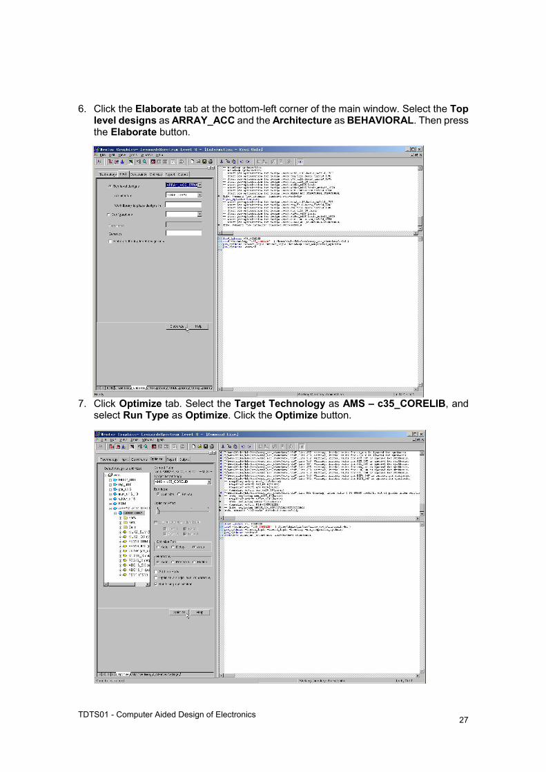
6. Click the Elaborate tab at the bottom-left corner of the main window. Select the Top level designs as ARRAY_ACC and the Architecture as BEHAVIORAL. Then press the Elaborate button.
7. Click Optimize tab. Select the Target Technology as AMS – c35_CORELIB, and select Run Type as Optimize. Click the Optimize button.

TDTS01 - Computer Aided Design of Electronics 28
8. Click Report tab. Click Report Area tab at the bottom-left corner of the main window. Specify the Report Filename as behavioral.area and press the Report Area button to save the area report.
9. On the Report tab. Click Report Delay tab at the bottom-left corner of the main window. Specify the Report Filename as behavioral.delay and press the Report Delay button to save the delay report.
10. Pay attention to the settings such as “Optimize effort” and “Optimize For”. Since the “behavioral” architecture has aimed the performance as design metric, select “delay” for “Optimize For”. Higher effort level may result in smaller delay, but will increase the optimization time. You can experience this and write your observations in the report. Note that the tool does not allow some combinations of “Optimize effort” and “Optimize For”.
11. Click Output tab. Choose Format as Verilog (*.v). Specify the file name as behavioral.v and press the Write button to save the netlist file.
12. Repeat from point 6 for “LESS_STATES” as architecture. Pay attention to change file names accordingly in order to keep the files you have created before. This design is for “area” metric, therefore, select the “Optimization” options accordingly. For point 11 use less_states.v as exported netlist file name.
13. Close LeonardoSpectrum and get back to the Unix terminal.

TDTS01 - Computer Aided Design of Electronics 29
14. Inspect the area reports.
cat behavioral.area
cat less_states.area
We can see how many instances of each primitive from the library c35_CORELIB is used, what are the approximated areas for them, what is the total count of the utilized primitives and the most important metric is “Number of um2” which shows the overall area for the designs.
What is the area difference between these two designs? Write your interpretation in the report.
The area depends on the technology (given in the library) as well as the design. Knowing the breakdown of the area may help the designer in improving it. However, it should be mentioned that by the advancement of the technology and shrinkage of the feature sizes, the area metric is becoming less and less important while the power issues are becoming more and more important.
Please put copies of the area reports in your final report. You may use a screen shot as well. On a Solaris workstation, an application called “SnapShot” can be used to capture screen shots.
15. Inspect the delay report.
cat behavioral.delay
cat less_states.delay
Here, we focus on “Clock Frequency Report”. It might be reported for clock signal or its negate, e.g. CLK or NOT_CLK, depending on the design. What is the clock frequency difference between these two designs? Write your interpretation in the report. LeonardoSpectrum finds and reports the critical paths “Critical path #n”. They are indexed by natural numbers (#n) and might be a number of them or only one. Identifying the critical path is critical to improve the design performance. Finding the critical path is not always feasible for a human designer especially that it may depend on the technology (given in the library) as well. Then the designer may look for ways to shorten this path.
Please put copies of the delay reports in your final report. You may use a screen shot as well.
It is worth mentioning that the important metrics for a design include delay, area, power, reliability, and testability. Unfortunately, there are tradeoffs between them. For example there are well-known techniques to tradeoff area vs. other metrics.

Chapter 6 Tutorial of Design for Testing
In the previous chapters, you have learned how to synthesize a design down to the gate level. Sometimes designs have very low testability. In order to improve the testability, modifications to the original design are required, while the functionality of the design should remain the same. There are a few techniques to revise the design and improve the testability (some of them are automated). But it is not easy for a designer, as a human, to immediately and exactly see how testable a design is. Here CAD tools will help the designer in order to evaluate the testability of a design.
In order to test a manufactured chip, test patterns are applied to it. But what is a minimum set of test patterns to cover as much faults as possible? Here again CAD tools help to find a very good set of test patterns with a minimal size (in fact test application time is important) and a maximal coverage.
In this chapter, you will learn to use FastScan to automatically generate test patterns and get the testability statistics. Then we will use DFTAdvisor which is a tool that automatically modifies the design in order to improve its testability. FastScan and DFTAdvisor are parts of TESSENT and therefore we need to load the TESSENT module (Also see end of chapter 3).
% module add prog/mentor/tessent
Please pay attention that by adding the module its path is “usually” added to the beginning of the environmental variable PATH. In order to make sure do echo $PATH At its beginning you should see /sw/mentor/tessent/bin otherwise add it manually as follows. Note that even if the module is loaded, you need to check for its path in PATH.
% setenv PATH /sw/mentor/tessent/bin:$PATH
In order to automatically generate test patterns, The ATPG library which contains scan flip-flops for the specified technology is required. In the lab we use a library for AMS c35 technology. You can obtain one copy of this ATPG library file from the /home/TDTS01/example. Copy the file c35_CORELIB.atpg from there to the desirable directory which also contains your synthesized design (It is a file in verilog, *.v, format that you generated and saved in synthesis chapter). In the following we assume that the desired directory is /home/u_name/TDTS01/example.
Change your working directory to: /home/u_name/TDTS01/example/
Therefore, % pwd should give: /home/u_name/TDTS01/example
And, % ls results should contain the following
behavioral.v,
less_states.v, and
c35_CORELIB.atpg.

TDTS01 - Computer Aided Design of Electronics 31
We will first try to improve the testability manually (section 6.1) and then we use an automatic Design For Testing (DFT) method (section 6.2).
6.1 Automatic Test Pattern Generation Now we are ready to start with FastScan.
1. Invoke FastScan:
% fastscan behavioral.v -lib c35_CORELIB.atpg
2. Read the messages; except “Warning: 8 cases: Unused net in DFT
library model”, should not be other warnings or errors.
3. Type “report primary inputs” and pay attention to the CLK and RST in the list. These inputs are special inputs for clock and reset signals.
4. These special inputs are non-data signals that propagate to (almost) all memory elements in your design and therefore should be explicitly declared to the FastScan. These inputs are identified by the general name of clocks in the FastScan. Declare them as follows:
add clocks 0 CLK
add clocks 0 RST
5. In order to check if they are correctly added do the following:
report clocks
The response should be:
/CLK off-state = 0
/RST off-state = 0
In case you have entered a wrong entry, use the following to remove it.
delete clocks name_of_wrong_entry
Usually there are two primary pins that you may want to define as circuit clocks, CLK (clock) and RST (reset). Here a primary clock pin means that you use the rising or falling edge of the clock signal coming from this primary input port to trigger an event.
The off-State of a primary input clock should be defined as ‘0’ if you use its raising edge, or ‘1’ when using the falling edge.
6. Initial settings are done, change the mode to Automatic Test Pattern Generation (ATPG):
set system mode atpg
7. Create the test patterns:
create patterns
FastScan ATPG statistics will be displayed after some delay. You may get the statistics later by typing:
report STAT

TDTS01 - Computer Aided Design of Electronics 32
8. After “create patterns” look for “abort limit” on the screen. In case the pattern generation is taking too much time, you may decrease it by “set abort limit a_number”.
9. Save the test patterns.
save patterns behavioral.patterns -ascii
10. Exit.
exit
Pay attention to the following points. Please do not report the “test patterns” since they do not provide any important information for this lab. In case you are working on the example design (1st assignment), you are not expected to fully understand the results.
o test coverage: shows what percentage of detectable faults are covered by the
generated test patterns =𝑫𝒆𝒕𝒆𝒄𝒕𝒆𝒅 𝒇𝒂𝒖𝒍𝒕𝒔
𝑫𝒆𝒕𝒆𝒄𝒕𝒂𝒃𝒍𝒆 𝒇𝒂𝒖𝒍𝒕𝒔
o fault coverage: shows the ratio of the detectable faults to all possible faults
=𝑫𝒆𝒕𝒆𝒄𝒕𝒆𝒅 𝒇𝒂𝒖𝒍𝒕𝒔
𝑨𝒍𝒍 𝒑𝒐𝒔𝒔𝒊𝒃𝒍𝒆 𝒇𝒂𝒖𝒍𝒕𝒔
o # test patterns: number of generated test patterns
o CPU time: time it took to generate the test patterns
Repeat the above procedure for less_states.v. Include copies of the above statistics result for bahavioral.v and for less_states.v. Explain the differences and pay attention also to the run time of the program.

TDTS01 - Computer Aided Design of Electronics 33
6.2 Automatic Scan Chain Insertion In this section DFTAdvisor is used to insert scan chains into our designs. It is expected that the modified designs’ testabilities improve considerably.
1. Invoke DFTAdvisor:
% dftadvisor behavioral.v -lib c35_CORELIB.atpg
2. Read the messages; except “Warning: 8 cases: Unused net in DFT
library model”, should not be other warnings or errors.
3. Type “report primary inputs” and pay attention to the reported inputs and their relation to the original design’s ports. You can also see the outputs by typing “report primary outputs”.
4. Similar to FastScan, clock and reset signals are identified by the general name of clocks in the DFTAdvisor. Declare them as follows:
add clocks 0 CLK
add clocks 0 RST
5. In order to check if they are correctly added do the following:
report clocks
The response should be:
/CLK off-state = 0
/RST off-state = 0
In case you have entered a wrong entry, use the following to remove it.
delete clocks name_of_wrong_entry
6. Initial settings are done, change the mode to Design For Testing (DFT):
set system mode dft
7. The type of the scan chain should be declared to DFTAdvisor. We are interested in a comprehensive scan chain, therefore “full_scan” is selected:
setup scan identification full_scan
It is also possible to specify a partial scan chain, but we are not interested in that. Now that the type of scan chain is declared, DFTAdvisor can proceed by analyzing the original design and generate the scan chain. Type
run
So far, DFTAdvisor has displayed messaged regarding flip flops (registers, memory elements, or sequential instances) and if they can be used as scan flip flops. The asynchronous paths (CLK and RST) are also recognized. Then it is decided which flip flop will be included in the scan chain.
8. In order to insert the scan chain into the original design, type
insert test logic
Except “Warning: Flattened model has been freed”, there should not be other warnings or errors.

TDTS01 - Computer Aided Design of Electronics 34
9. In order to save the new design enhanced for testability, type
write netlist behavioral_scanChain.v
10. In order to save the setup that is necessary for ATPG tool, type
write atpg setup behavioral_atpgSetup
Now check in the corresponding directory. There should be two new files named behavioral_atpgSetup.dofile and behavioral_atpgSetup.testproc. Open these files (e.g., by cat behavioral_atpgSetup.dofile) and you can see settings and procedures that explains how the scan chain should be used. Pay attention that one of the files is referred to in the other one. These information will be used by the ATPG tool. Take care not to change these files.
11. Exit DFTAdvisor
exit
12. Now the design enhanced for testability is generated. It is time to generate the test patterns and evaluate the testability. Invoke FastScan:
% fastscan behavioral_scanChain.v -lib c35_CORELIB.atpg
13. Read the messages; except “Warning: 8 cases: Unused net in DFT
library model”, should not be other warnings or errors.
14. Type “report primary inputs” and pay attention to the difference between the inputs of behavioral.v and behavioral_scanChain.v. There should be two additional inputs related to the scan chain: scan_in1 and scan_en.
15. The dofile that was generated by DFTAdvisor is used to setup FastScan. Type
dofile behavioral_atpgSetup.dofile
16. Check the clocks:
report clocks
The response should be:
/CLK off-state = 0
/RST off-state = 0
This means that the dofile has added the clocks correctly.
17. Type “report primary outputs” and pay attention to the difference between the outputs of behavioral.v and behavioral_scanChain.v. Isn’t there a difference? Then where the outputs of scan chain are going to? Type the following to find out.
report scan chains
There should be at least one line about the scan chain that is introduced to FastScan by the dofile. Which output port is used as the scan chain’s output? One of the original design’s output ports might be re-used for this purpose.
18. Change system mode to atpg and generate the test patterns:
set system mode atpg
creat patterns
Are the testability results better now?

TDTS01 - Computer Aided Design of Electronics 35
19. Save the test patterns.
save patterns behavioral_scanChain.patterns -ascii
20. Exit.
exit
In case you are working on your own design for 4th assignment
o Please include the above statistics result (section 6.1 plus section 6.2) in your report. Do it for both of the original design and the design that you have modified for testability (section 6.1) and also for section 6.2. Describe the differences shortly.
o Please include area and delay reports (saved during the synthesis of the design) in your report. Do it for both of the original design and the design that you have modified for testability. Describe the differences shortly. (only for section 6.1)
o Usually, the extra circuitry added to improve the testability results in undesirable increase in area and delay. However, this is not always the case. Please write in your report which situation you are facing and what you think is the reason.

Attachments Codes for the Example (1st assignment)
1. Design’s VHDL code for the example 37
2. Testbench’s VHDL code for the example 40
3. Validation data file for the example 44
4. Do file for the example 44
5. Feedback forms 46

TDTS01 - Computer Aided Design of Electronics 37

TDTS01 - Computer Aided Design of Electronics 38

TDTS01 - Computer Aided Design of Electronics 39

TDTS01 - Computer Aided Design of Electronics 40
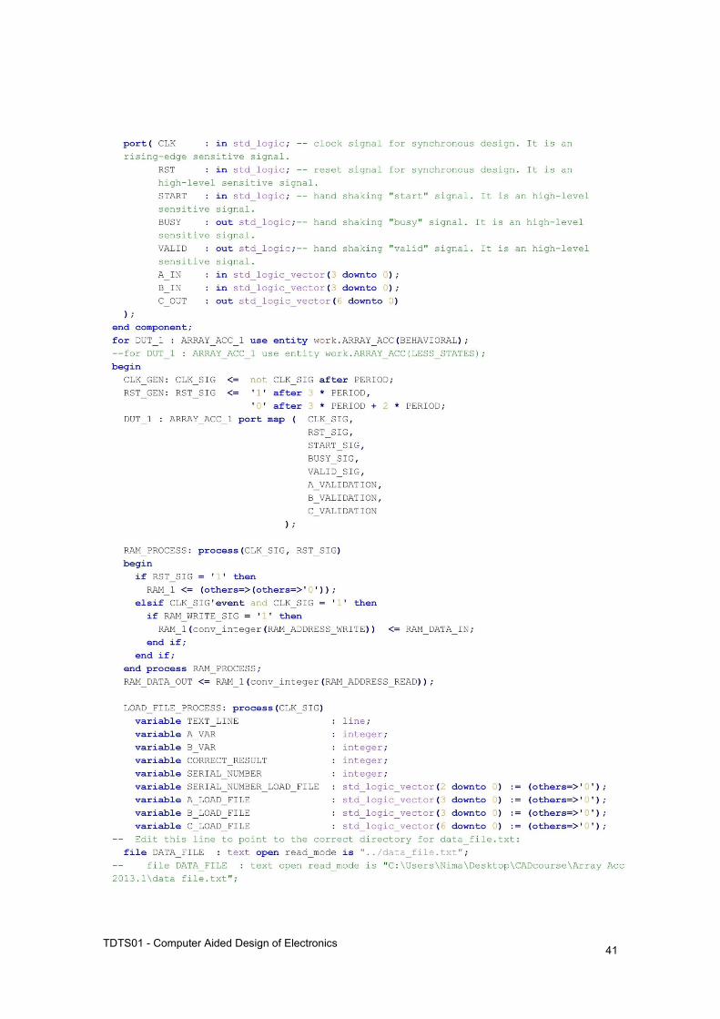
TDTS01 - Computer Aided Design of Electronics 41

TDTS01 - Computer Aided Design of Electronics 42

TDTS01 - Computer Aided Design of Electronics 43

TDTS01 - Computer Aided Design of Electronics 44
Validation Data File
Do file
0 2 1
1 3 7
2 5 4
3 9 8
4 39
0 2 1
1 3 7
2 5 4
3 0 8
4 30
0 2 1
1 3 7
2 5 4
3 11 8
4 41
vcom *.vhd
vsim -gui work.test_bench
add wave sim:/test_bench/*
add wave sim:/test_bench/DUT_1/*
run 5 us

Page is left blank intentionally.

TDTS01 - Computer Aided Design of Electronics 46
Feedback Form for 1st Assignment:
Project Specification and Tool-Set Experience
Please help us improve by filling this feedback-form individually (two copies if you are two in a group).
What program are you from (COS, D, IT, SOC, Y, Exchange)?
Are you working alone or in a group of two?
How much did you learn by doing this assignment?
How much did you know about the topic before doing this assignment?
How easy was this assignment?
How interesting was this assignment?
How much time did it take?
What did you like/dislike, any suggestions?

TDTS01 - Computer Aided Design of Electronics 47
Page is left blank intentionally.

TDTS01 - Computer Aided Design of Electronics 48
Feedback Form for 1st Assignment:
Project Specification and Tool-Set Experience
Please help us improve by filling this feedback-form individually (two copies if you are two in a group).
What program are you from (COS, D, IT, SOC, Y, Exchange)?
Are you working alone or in a group of two?
How much did you learn by doing this assignment?
How much did you know about the topic before doing this assignment?
How easy was this assignment?
How interesting was this assignment?
How much time did it take?
What did you like/dislike, any suggestions?

TDTS01 - Computer Aided Design of Electronics 49
Page is left blank intentionally.

TDTS01 - Computer Aided Design of Electronics 50
Feedback Form for 2nd Assignment:
Compilable Design and Testbench
Please help us improve by filling this feedback-form individually (two copies if you are two in a group).
What program are you from (COS, D, IT, SOC, Y, Exchange)?
Are you working alone or in a group of two?
How much did you learn by doing this assignment?
How much did you know about the topic before doing this assignment?
How easy was this assignment?
How interesting was this assignment?
How much time did it take?
What did you like/dislike, any suggestions?

TDTS01 - Computer Aided Design of Electronics 51
Page is left blank intentionally.

TDTS01 - Computer Aided Design of Electronics 52
Feedback Form for 2nd Assignment:
Compilable Design and Testbench
Please help us improve by filling this feedback-form individually (two copies if you are two in a group).
What program are you from (COS, D, IT, SOC, Y, Exchange)?
Are you working alone or in a group of two?
How much did you learn by doing this assignment?
How much did you know about the topic before doing this assignment?
How easy was this assignment?
How interesting was this assignment?
How much time did it take?
What did you like/dislike, any suggestions?

TDTS01 - Computer Aided Design of Electronics 53
Page is left blank intentionally.

TDTS01 - Computer Aided Design of Electronics 54
Feedback Form for 3rd Assignment:
Synthesizable Design
Please help us improve by filling this feedback-form individually (two copies if you are two in a group).
What program are you from (COS, D, IT, SOC, Y, Exchange)?
Are you working alone or in a group of two?
How much did you learn by doing this assignment?
How much did you know about the topic before doing this assignment?
How easy was this assignment?
How interesting was this assignment?
How much time did it take?
What did you like/dislike, any suggestions?

TDTS01 - Computer Aided Design of Electronics 55
Page is left blank intentionally.

TDTS01 - Computer Aided Design of Electronics 56
Feedback Form for 3rd Assignment:
Synthesizable Design
Please help us improve by filling this feedback-form individually (two copies if you are two in a group).
What program are you from (COS, D, IT, SOC, Y, Exchange)?
Are you working alone or in a group of two?
How much did you learn by doing this assignment?
How much did you know about the topic before doing this assignment?
How easy was this assignment?
How interesting was this assignment?
How much time did it take?
What did you like/dislike, any suggestions?

TDTS01 - Computer Aided Design of Electronics 57
Page is left blank intentionally.

TDTS01 - Computer Aided Design of Electronics 58
Feedback Form for 4th Assignment:
Manufacturing Test
Please help us improve by filling this feedback-form individually (two copies if you are two in a group).
What program are you from (COS, D, IT, SOC, Y, Exchange)?
Are you working alone or in a group of two?
How much did you learn by doing this assignment?
How much did you know about the topic before doing this assignment?
How easy was this assignment?
How interesting was this assignment?
How much time did it take?
What did you like/dislike, any suggestions?

TDTS01 - Computer Aided Design of Electronics 59
Page is left blank intentionally.

TDTS01 - Computer Aided Design of Electronics 60
Feedback Form for 4th Assignment:
Manufacturing Test
Please help us improve by filling this feedback-form individually (two copies if you are two in a group).
What program are you from (COS, D, IT, SOC, Y, Exchange)?
Are you working alone or in a group of two?
How much did you learn by doing this assignment?
How much did you know about the topic before doing this assignment?
How easy was this assignment?
How interesting was this assignment?
How much time did it take?
What did you like/dislike, any suggestions?


