TE0221 ANALOG AND DIGITAL SYSTEM LAB Laboratory Manual DEPARTMENT OF TELECOMMUNICATION ENGINEERING SRM UNIVERSITY S.R.M. NAGAR, KATTANKULATHUR – 603 203. FOR PRIVATE CIRCULATION ONLY ALL RIGHTS RESERVED
Transcript
TE0221 ANALOG AND DIGITAL SYSTEM LAB
Laboratory Manual
DEPARTMENT OF TELECOMMUNICATION ENGINEERING
SRM UNIVERSITY
S.R.M. NAGAR, KATTANKULATHUR – 603 203.
FOR PRIVATE CIRCULATION ONLY
ALL RIGHTS RESERVED
DEPARTMENT OF TELECOMMUNICATION ENGINEERING
TE0221
ANALOG AND DIGITAL SYSTEM LAB
(2011-2012)
Revision No: 3 PREPARED BY, Date:
Mrs. N. Showme Mr. Vemula Ramkishore
HOD/TCE
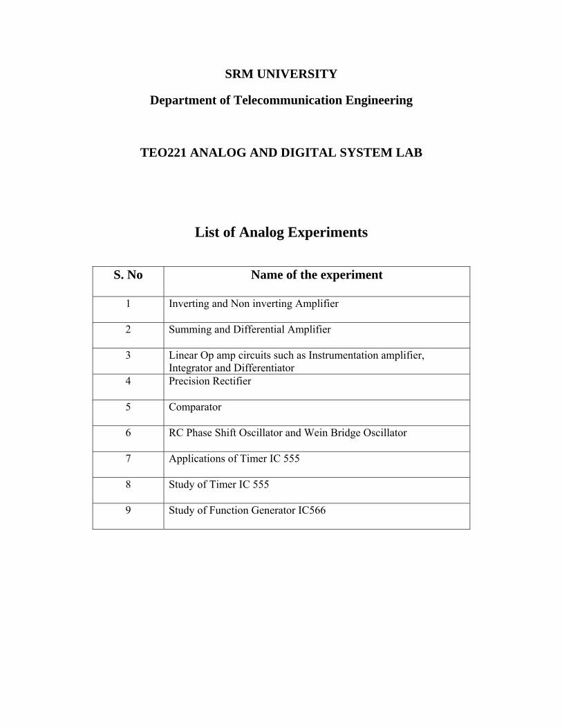
SRM UNIVERSITY
Department of Telecommunication Engineering
TEO221 ANALOG AND DIGITAL SYSTEM LAB
List of Analog Experiments
S. No Name of the experiment
1 Inverting and Non inverting Amplifier
2 Summing and Differential Amplifier
3 Linear Op amp circuits such as Instrumentation amplifier, Integrator and Differentiator
4 Precision Rectifier
5 Comparator
6 RC Phase Shift Oscillator and Wein Bridge Oscillator
7 Applications of Timer IC 555
8 Study of Timer IC 555
9 Study of Function Generator IC566
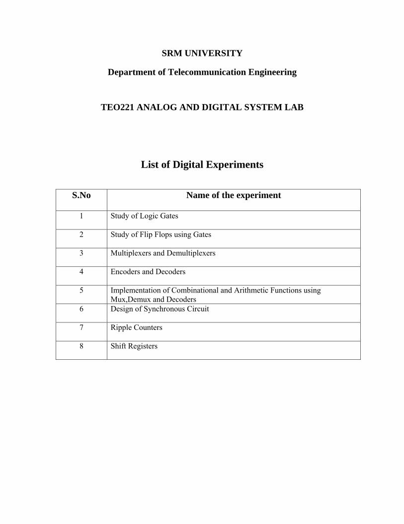
SRM UNIVERSITY
Department of Telecommunication Engineering
TEO221 ANALOG AND DIGITAL SYSTEM LAB
List of Digital Experiments
S.No Name of the experiment
1 Study of Logic Gates
2 Study of Flip Flops using Gates
3 Multiplexers and Demultiplexers
4 Encoders and Decoders
5 Implementation of Combinational and Arithmetic Functions using Mux,Demux and Decoders
6 Design of Synchronous Circuit
7 Ripple Counters
8 Shift Registers
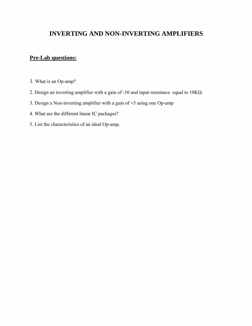
INVERTING AND NON-INVERTING AMPLIFIERS
Pre-Lab questions:
1. What is an Op-amp?
2. Design an inverting amplifier with a gain of -10 and input resistance equal to 10KΩ.
3. Design a Non-inverting amplifier with a gain of +5 using one Op-amp
4. What are the different linear IC packages?
5. List the characteristics of an ideal Op-amp.
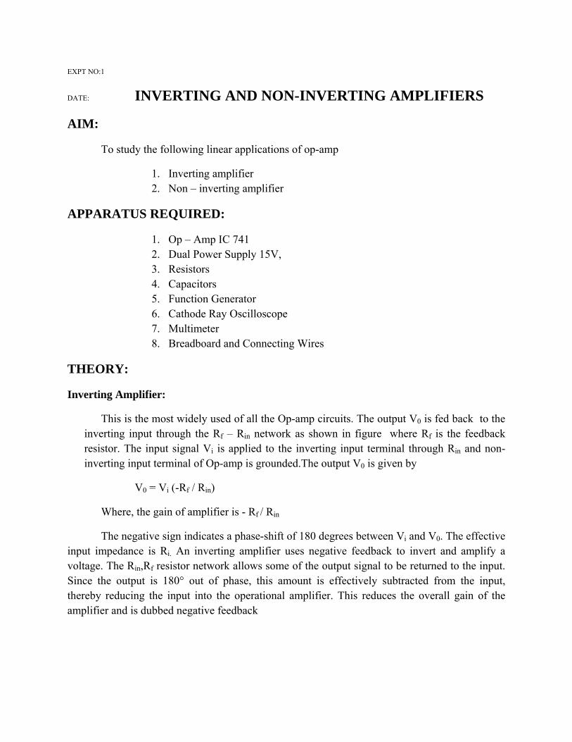
EXPT NO:1
DATE: INVERTING AND NON-INVERTING AMPLIFIERS
AIM:
To study the following linear applications of op-amp
1. Inverting amplifier 2. Non – inverting amplifier
APPARATUS REQUIRED:
1. Op – Amp IC 741 2. Dual Power Supply 15V, 3. Resistors 4. Capacitors 5. Function Generator 6. Cathode Ray Oscilloscope 7. Multimeter 8. Breadboard and Connecting Wires
THEORY:
Inverting Amplifier:
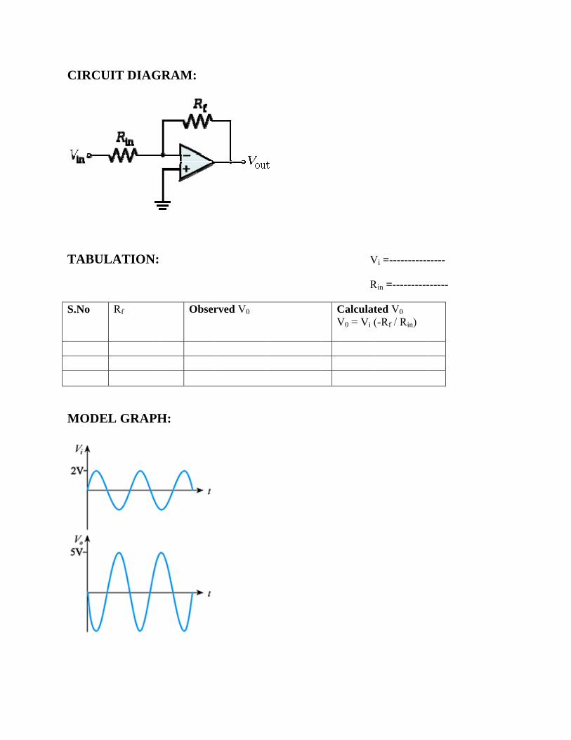
This is the most widely used of all the Op-amp circuits. The output V0 is fed back to the inverting input through the Rf – Rin network as shown in figure where Rf is the feedback resistor. The input signal Vi is applied to the inverting input terminal through Rin and non-inverting input terminal of Op-amp is grounded.The output V0 is given by
V0 = Vi (-Rf / Rin)
Where, the gain of amplifier is - Rf / Rin
The negative sign indicates a phase-shift of 180 degrees between Vi and V0. The effective input impedance is Ri. An inverting amplifier uses negative feedback to invert and amplify a voltage. The Rin,Rf resistor network allows some of the output signal to be returned to the input. Since the output is 180° out of phase, this amount is effectively subtracted from the input, thereby reducing the input into the operational amplifier. This reduces the overall gain of the amplifier and is dubbed negative feedback
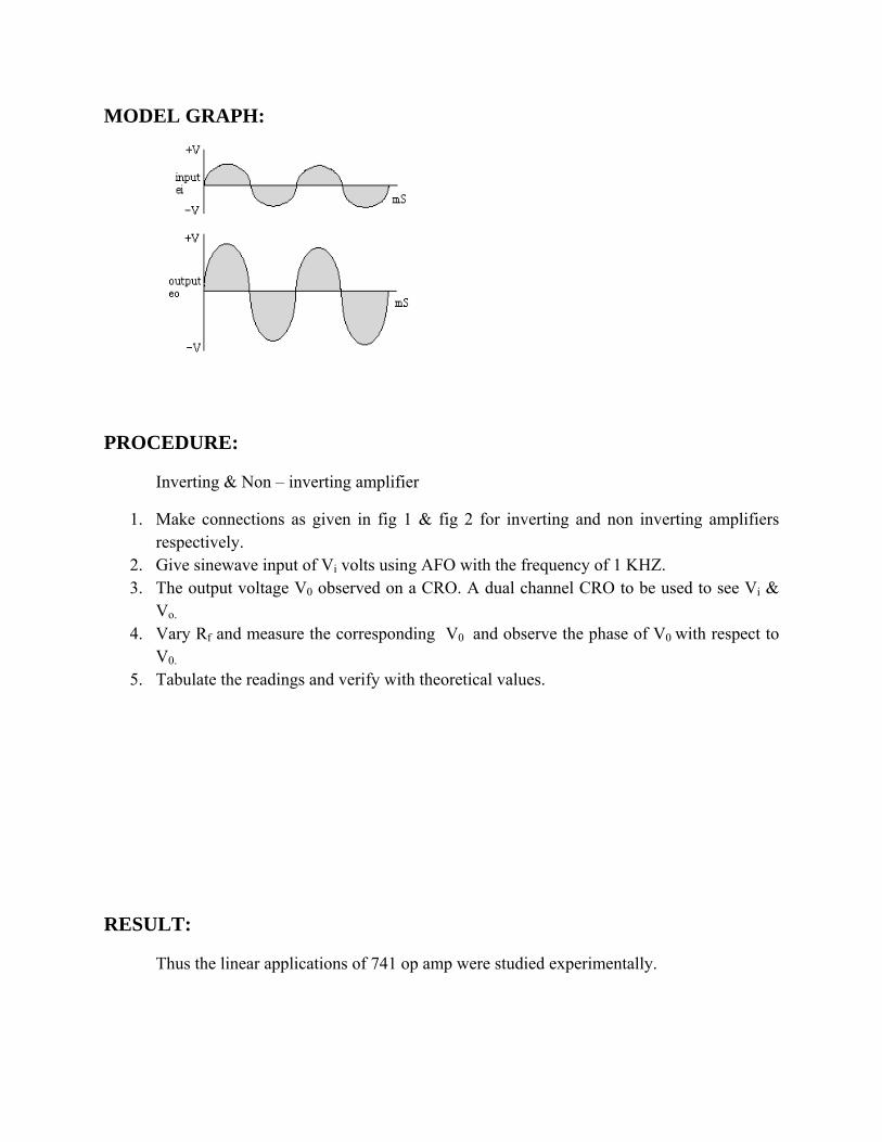
1. Make connections as given in fig 1 & fig 2 for inverting and non inverting amplifiers respectively.
2. Give sinewave input of Vi volts using AFO with the frequency of 1 KHZ. 3. The output voltage V0 observed on a CRO. A dual channel CRO to be used to see Vi &
Vo. 4. Vary Rf and measure the corresponding V0 and observe the phase of V0 with respect to
V0. 5. Tabulate the readings and verify with theoretical values.
RESULT:
Thus the linear applications of 741 op amp were studied experimentally.
Post Lab Questions:
1. What is the input impedance of a non inverting op-amp amplifier?
2. If the open loop gain of an op-amp is very large, does the closed loop gain depend upon the external components or the op-amp?
3. Define common mode rejection ratio
4. Explain the meaning of open loop and closed loop operation of an op- amp?
5. What is a practical op-amp? Draw its equivalent circuit.
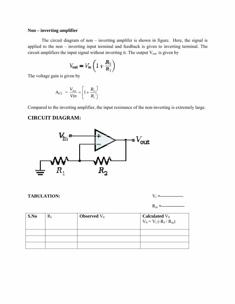
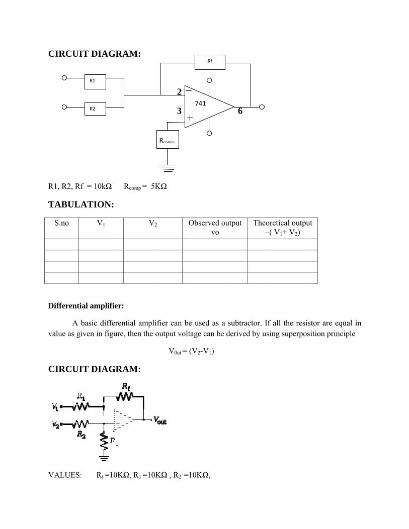
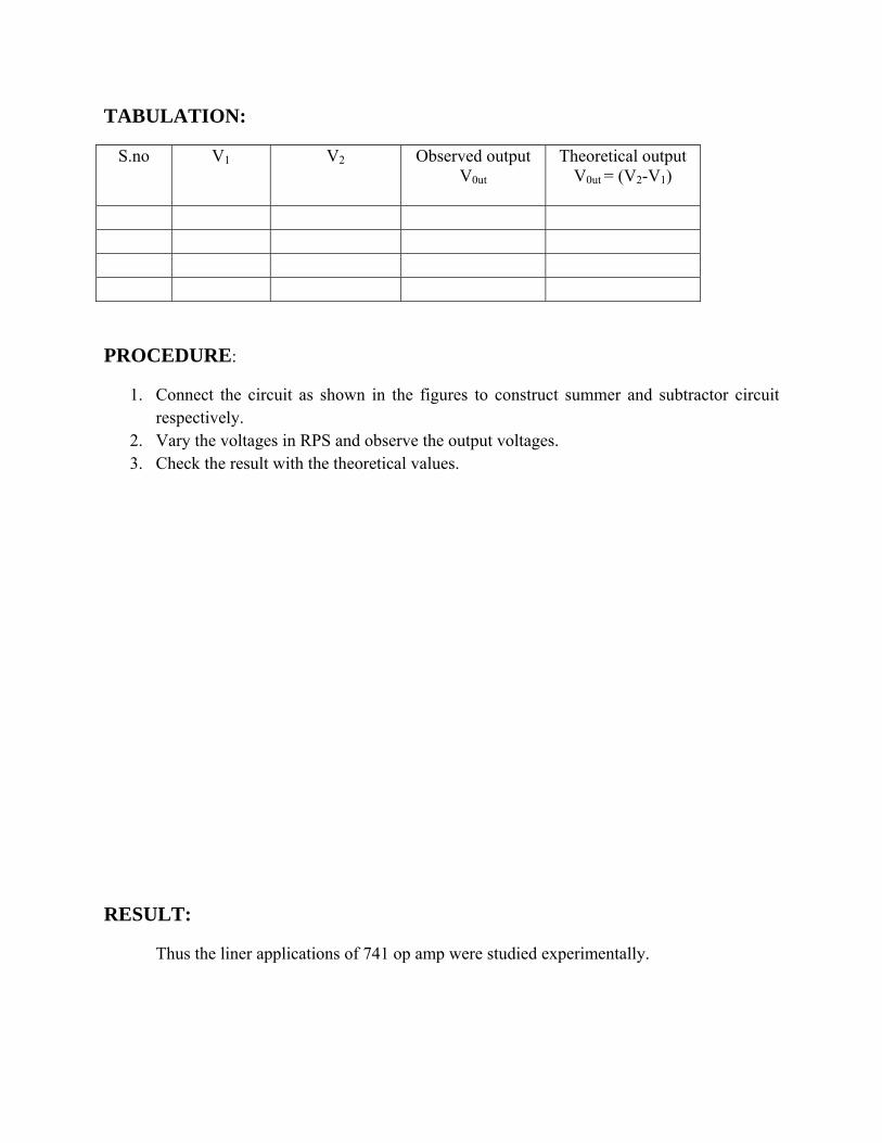
SUMMING AND DIFFERENTIAL AMPLIFIER
Pre-Lab questions:
1. What is a Differential amplifier 2. Define a Summing amplifier 3. Define difference mode gain and common mode gain 4. Give the applications of summing and differential amplifier
EXPT NO:2
DATE: SUMMING AND DIFFERENTIAL AMPLIFIER
AIM:
To study the operation of IC741 as
a) Summing Amplifier b) Differential Amplifier
APPARATUS REQUIRED:
1. Op-Amp IC 741 2. Dual power Supply 15V 3. Resistor 4. Capacitors 5. Function Generator 6. Cathode Ray Oscilloscope 7. Multimeter 8. Breadboard and Connecting wires.
THEORY:
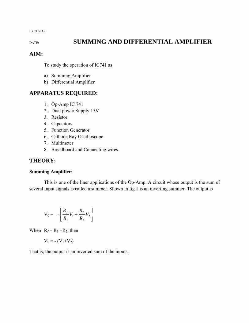
Summing Amplifier:
This is one of the liner applications of the Op-Amp. A circuit whose output is the sum of several input signals is called a summer. Shown in fig.1 is an inverting summer. The output is
V0 = - ⎥⎦
⎤⎢⎣
⎡+ 2
21
1
VRR
VRR ff
When Rf = R1 =R2, then
V0 = - (V1+V2)
That is, the output is an inverted sum of the inputs.
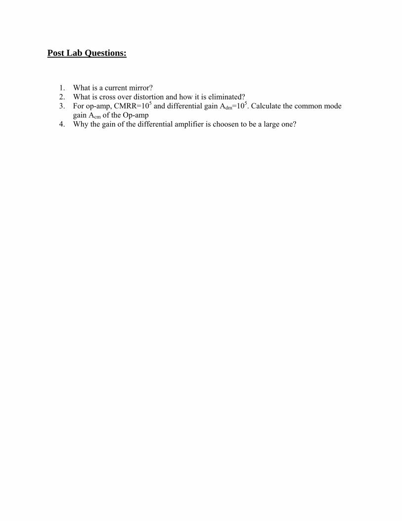
circuit as shown in the figures to construct summer and subtractor circuit respectively.
ult with the theoretical values.
ESULT:
he liner applications of 741 op amp were studied experimentally.
1. Connect the
2. Vary the voltages in RPS and observe the output voltages. 3. Check the res
R
Thus t
Post Lab Questions:
irror? 2. What is cross over distortion and how it is eliminated? 3. For op-amp, CMRR=105 and differential gain Adm=105. Calculate the common mode
1. What is a current m
gain Acm of the Op-amp 4. Why the gain of the differential amplifier is choosen to be a large one?
LINEAR OP AMP CIRCUITS SUCH AS INSTRUMENTATION AMPLIFIER, INTEGRATOR AND DIFFERENTIATOR
Pre-Lab questions:
ures of an instrumentation amplifier 2. What is an instrumentation amplifier? Draw a system whose gain is controlled by an
adjustable resistance.
that will eliminate these limitations ing initial conditions
1. What are the feat
3. What is an integrator and a differentiator? 4. What are the limitations of an ordinary op-amp differentiator? Draw the circuit of a
practical differentiator5. Draw the circuit of a Lossy integrator show
EXPT NO:3
ATE: LINEAR OP AMP CIRCUITS SUCH AS INSTRUMENTATION AMPLIFIER, INTEGRATOR
AIM:
To verify the linear op am instrumentation amplifier, Integrator and tiator.
or
entational) amplifier is a type of differential amplifier that tted with input buffers, which eliminate the need for input impedance matching
and thus make the amplifier particularly suitable for use in measurement and test equipment. Additio
circuit is
D
AND DIFFERENTIATOR
p circuit such asdifferen
APPARATUS REQUIRED:
1.Resist
2.Capacitor
3.AFO
4.OpAmp
5.Dual Supply
6.CRO
7.Bread Board
THEORY:
An instrumentation (or instrumhas been outfi
nal characteristics include very low DC offset, low drift, low noise, very high open-loop gain, very high common-mode rejection ratio, and very high input impedances. Instrumentation amplifiers are used where great accuracy and stability of the circuit both short- and long-term are required.
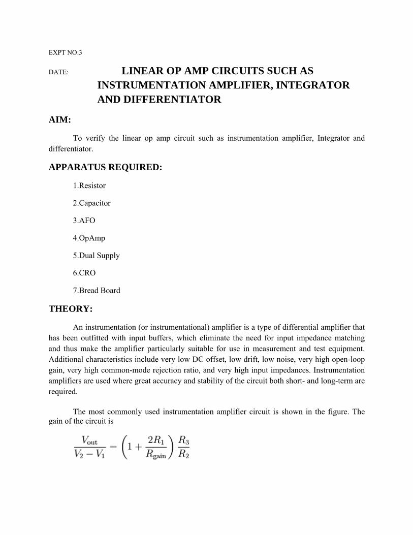
The most commonly used instrumentation amplifier circuit is shown in the figure. The gain of the
e feedback capacitor C begins to charge up, its reactance Xc decreases this results in the ratio of Xc/Rin increasing producing an output
plifier swings heavily to one voltage supply rail or the other with little or no control in between. The ideal voltage
at its input as the current through the feedback loop charges or discharges the capacitor as the required negative feedback occurs through the capacitor.
When a voltage, Vin is firstly applied to the input of an integrating amplifier, the uncharged capacitor C has very little resistance and acts a bit like a short circuit (voltage follower circuit) giving an overall gain of less than one. No current flows into the amplifiers input and point X is a virtual earth resulting in zero output. As th
voltage that continues to increase until the capacitor is fully charged.
At this point the capacitor acts as an open circuit, blocking anymore flow of DC current. The ratio of feedback capacitor to input resistor (Xc/Rin) is now infinite resulting in infinite gain. The result of this high gain (similar to the op-amps open-loop gain), is that the output of the amplifier goes into saturation .Saturation occurs when the output voltage of the am
output for the Integrator Amplifier as:
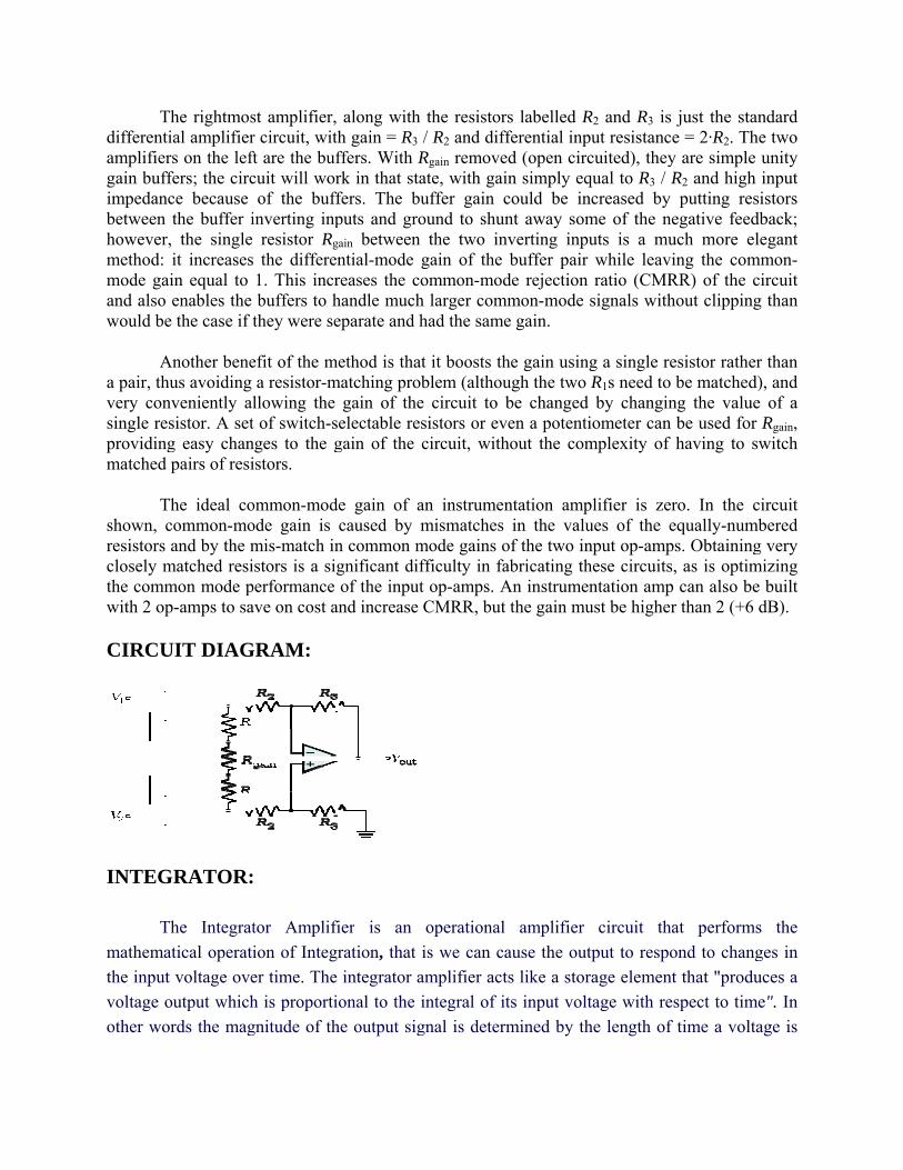
CIRCUIT DIAGRAM:
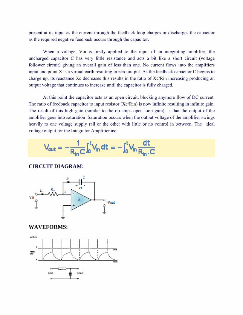
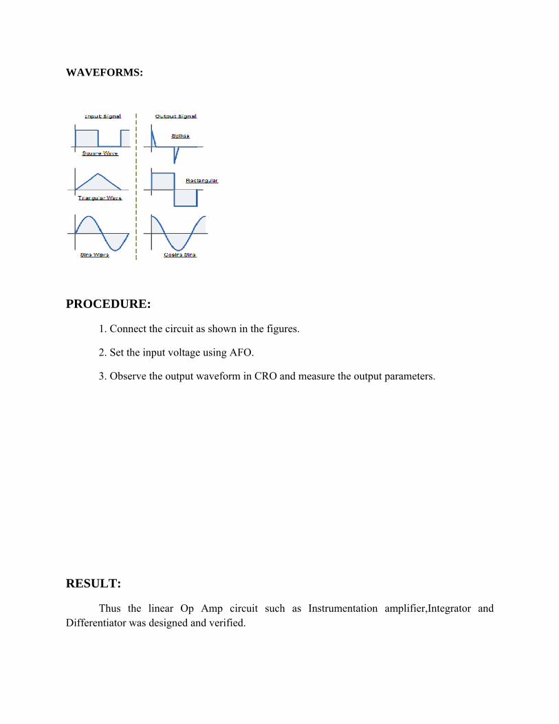
WAVEFORMS:
DIFFERENTIATOR:
A Differentiator is a circuit that is designed such that the output of the circuit is proportional to the derivative of the input. It creates an output voltage proportional to the rate of change of the input voltage. This leads to cool applications such as extracting edges for, square waves, converting sine waves into cosines and c hanging triangle waves into square waves. But most circuits are susceptible to some trouble and this one’s vulnerabilities are instability and noise. However, remedies are available to duce the troubles without losing the desired
n and higher output voltage from the differentiator amplifier.
refunction.
The input signal to the differentiator is applied to the capacitor. The capacitor blocks any DC content so there is no current flow to the amplifier summing point, X resulting in zero output voltage. The capacitor only allows AC type input voltage changes to pass through and whose frequency is dependant on the rate of change of the input signal. At low frequencies the reactance of the capacitor is "High" resulting in a low gain (Rf/Xc) and low output voltage from the op-amp. At higher frequencies the reactance of the capacitor is much lower resulting in a higher gai
However, at high frequencies a differentiator circuit becomes unstable and will start to oscillate. This is due mainly to the first-order effect, which determines the frequency response of the op-amp circuit causing a second-order response which, at high frequencies gives an output voltage far higher than what would be expected. To avoid this the high frequency gain of the circuit needs to be reduced by adding an additional small value capacitor across the feedback resistor Rf. Ideal voltage output for the Differentiator Amplifier is given as:
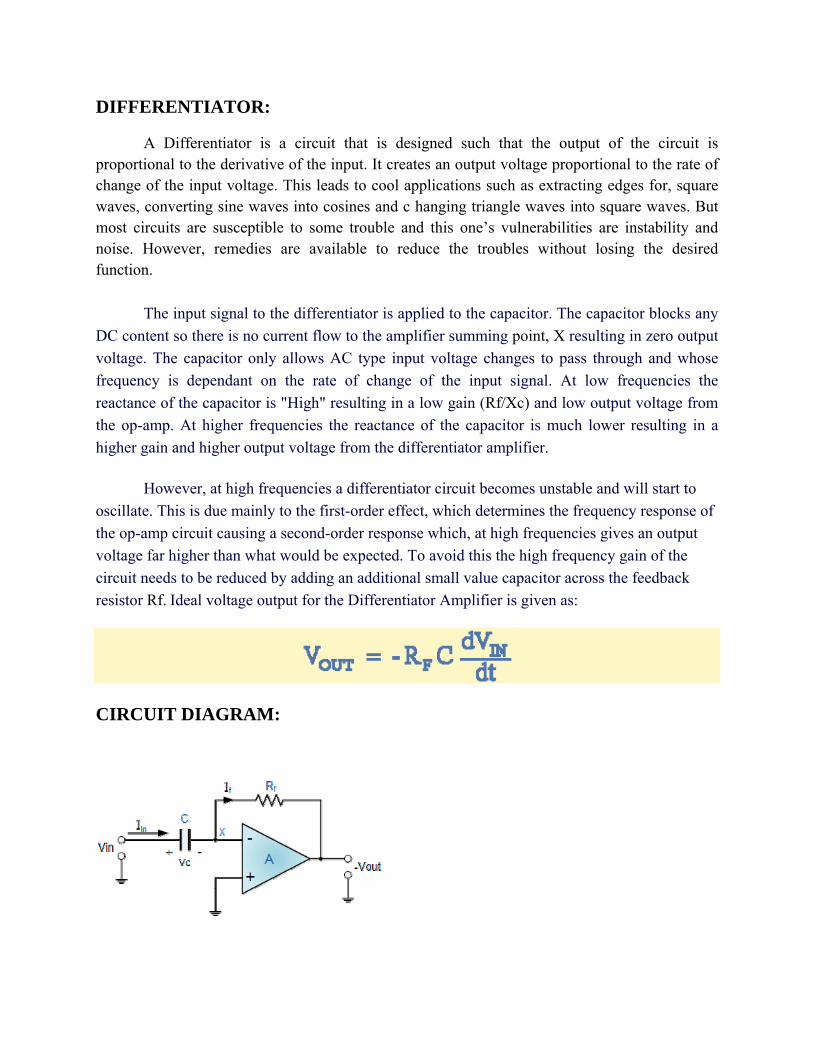
CIRCUIT DIAGRAM:
WAVEFORMS:
PROCEDURE:
1. Connect the circuit as shown in the figures.
2. Set the input voltage using AFO.
3. Observe the output waveform in CRO and measure the output parameters.
ESULT:
Thus the linear Op Amp circuit such as Instrumentation amplifier,Integrator and Differentiator was designed and verified.
R
Post Lab Questions:
in why integrators are preferred over differentiators in analog computer 2. What are the applications of integrator and differentiator 3.
ion amplifier commercially available 5. What is the function of an instrumentation amplifier?
1. Expla
Give the Practical applications of instrumentation amplifier 4. What are the monolithic instrumentat
PRECISION RECTIFIER
Pre-Lab questions:
1. What is a precision diode 2. Give the uses of precision diode 3. Give some applications of precision diode 4. What are the major limitations of an ordinary diode 5. Define a half wave rec
tifier and a full wave rectifier
EXPT NO:4
ATE: PRECISION RECTIFIER
IM:
To construct precision half wave rectifier and full wave rectifier using Op Amp.
APPARATUS REQUIRED:
1.Resistor
rd
THEO
itation of ordinary diodes is that it cannot rectify voltage below 0.6v,the cutin voltage of the diode.The precision rectifier, which is also known as a super diode, is a configuration obtained with an operational amplifier in order to have a circuit behaving like an ideal di n be useful for high-precision signal processing.
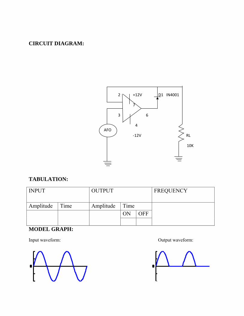
HALF WAVE RECTIFIER:
wave rectifier is an electronic circuit. The rectifier circuit takes alternating current C) f he
he uctor
D
A
2.IC 741
3.AFO
4.Diode IN 4001
5.Connecting wires
6.CRO
7.Bread boa
RY:
The major lim
ode and rectifier.It ca
A half-(A rom the wall outlet and converts it into a positive direct current (DC) output. Tparticular electronic device that accomplishes this task is a semiconductor called a diode. Tdiode like all semiconductors is a material which has a resistance in between that of a condor wire and an insulator like that of a plastic.
CIRC
2 D1 IN4001
7
3 6
4
‐12V RL
10K
NPUT OUTPUT FREQUENCY
UIT DIAGRAM:
+12V
TABULATION:
I
Amplitude Time Amplitude Time ON OFF
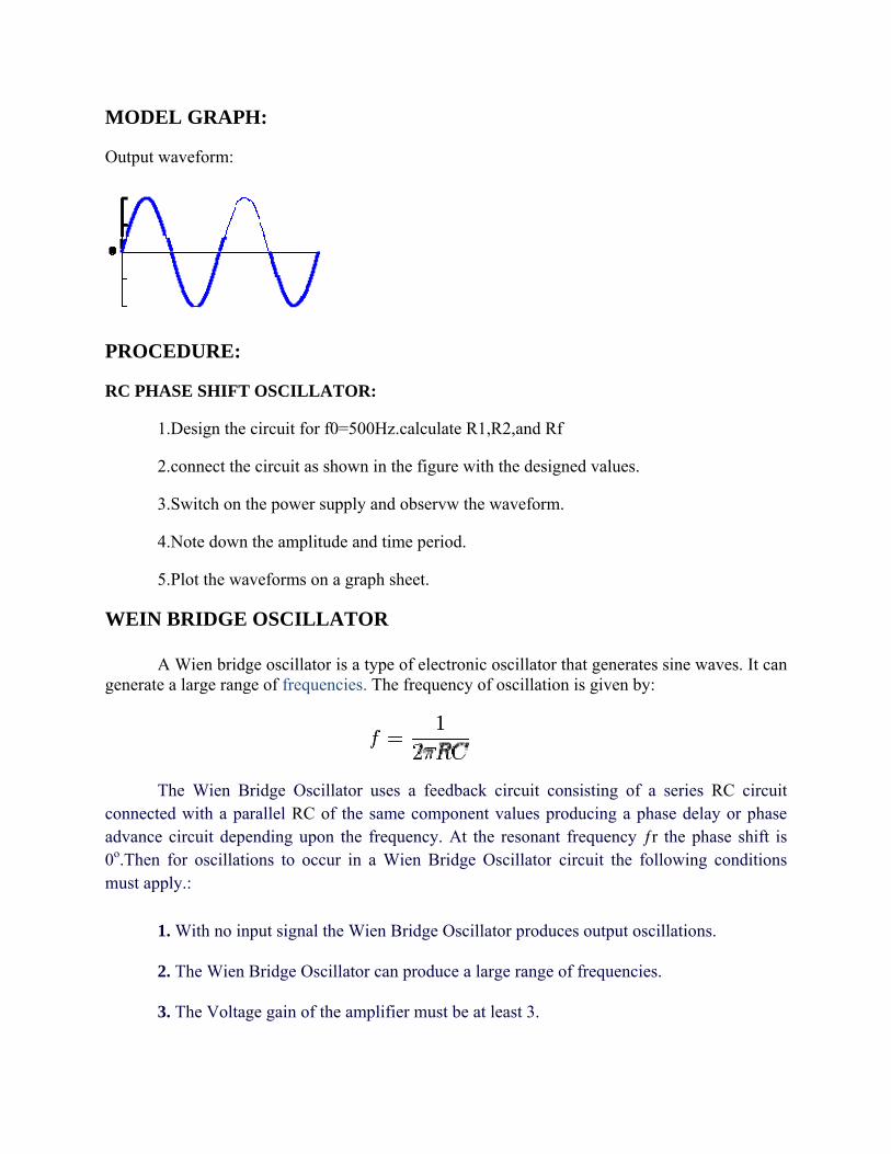
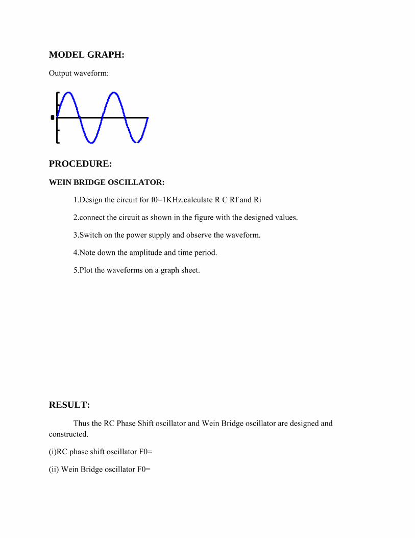
MODEL GRAPH:
Input waveform: Output waveform:
AFO
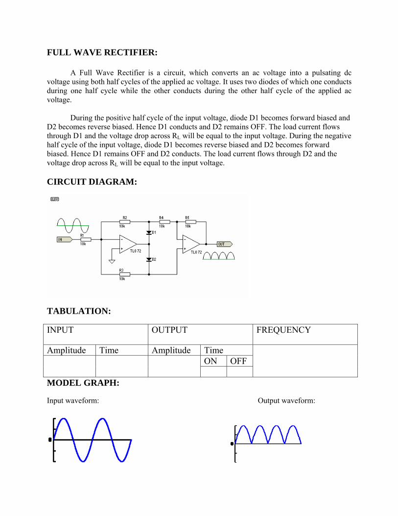
FULL WAVE RECTIFIER:
A Full Wa
during one half cycle while the other conducts durvoltage.
During the positivD2 becomethrough D1 and the voltage drop across Rhalf cycle of the input voltage, diode D1 bbiased. Hence D1 remains O
CIRCUIT DIAGRAM:
TABULATION:
ve Rectifier is a circuit, which converts an ac voltage into a pulsating dc cts
ing the other half cycle of the applied ac
e half cycle of the input voltage, diode D1 becomes forward biased and s reverse biased. Hence D1 conducts and D2 remains OFF. The load current flows
L will be equal to the input voltage. During the negative ecomes reverse biased and D2 becomes forward
FF nt flows through D2 and the t voltage.
INPUT OUTPUT FREQUENCY
voltage using both half cycles of the applied ac voltage. It uses two diodes of which one condu
and D2 conducts. The load currevoltage drop across RL will be equal to the inpu
Amplitude Time Amplitude Time ON OFF
MODEL GRAPH:
Input waveform: Output waveform:
PROCEDUR
1. Connect the circuit as shown in the figures
gnal voltage using AFO.
ESULT:
Thus the half wave rectifier and full wave rectifier are constructed and the output waveforms are drawn.
E:
for Half wave and Full wave rectifier.
2. Set the input si
3. Observe the output waveform in CRO and measure the output parameters.
R
Post Lab Questions:
1. Draw the circuit of a full wave rectifier and explain how it gives the average value 2. What is a Clipper and Clamper circuit 3. Draw the circuit of a clipper which will clip the input signal below a reference voltage 4. Draw the equivalent circuit of a full wave rectifier for input voltage less than zero
i<0)
volts(V
COMPARATOR
Pre-Lab questions:
1. What is a comparator circuit?
2. List the different types of comparator
3. Give the applications of comparator
4. Give the applications of Non linear op amp circuits
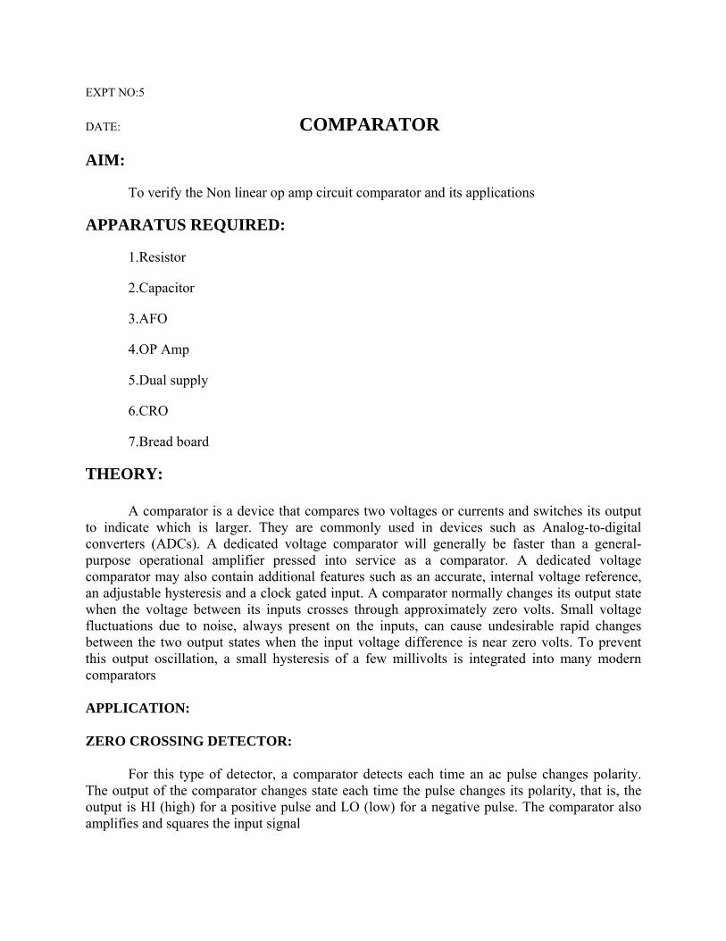
EXPT NO:5
ATE: COMPARATOR
AIM:
To verify the Non linear op amp circuit comparator and its applications
PPARATUS REQUIRED:
1.Resistor
2.Capacitor
3.AFO
Amp
tor is a device that compares two voltages or currents and switches its output to indicate which is larger. They are commonly used in devices such as Analog-to-digital convert A dedicated voltage comparator will generally be faster than a general-purpose operational amplifier pressed into service as a comparator. A dedicated voltage compar y also contain additional features such as an accurate, internal voltage reference, an adju resis and a clock gated input. A comparator normally changes its output state when the voltage between its inputs crosses through approximately zero volts. Small voltage fluctuations due to noise, always present on the inputs, can cause undesirable rapid changes between the two output states when the input voltage difference is near zero volts. To prevent this output oscillation, a small hysteresis of a few millivolts is integrated into many modern comparators
APPLICATION:
ZERO CROSSING DETECTOR:
D
A
4.OP
5.Dual supply
6.CRO
7.Bread board
THEORY:
A compara
ers (ADCs).
ator mastable hyste
For this type of detector, a comparator detects each time an ac pulse changes polarity. The output of the comparator changes state each time the pulse changes its polarity, that is, the output is HI (high) for a positive pulse and LO (low) for a negative pulse. The comparator also amplifies and squares the input signal
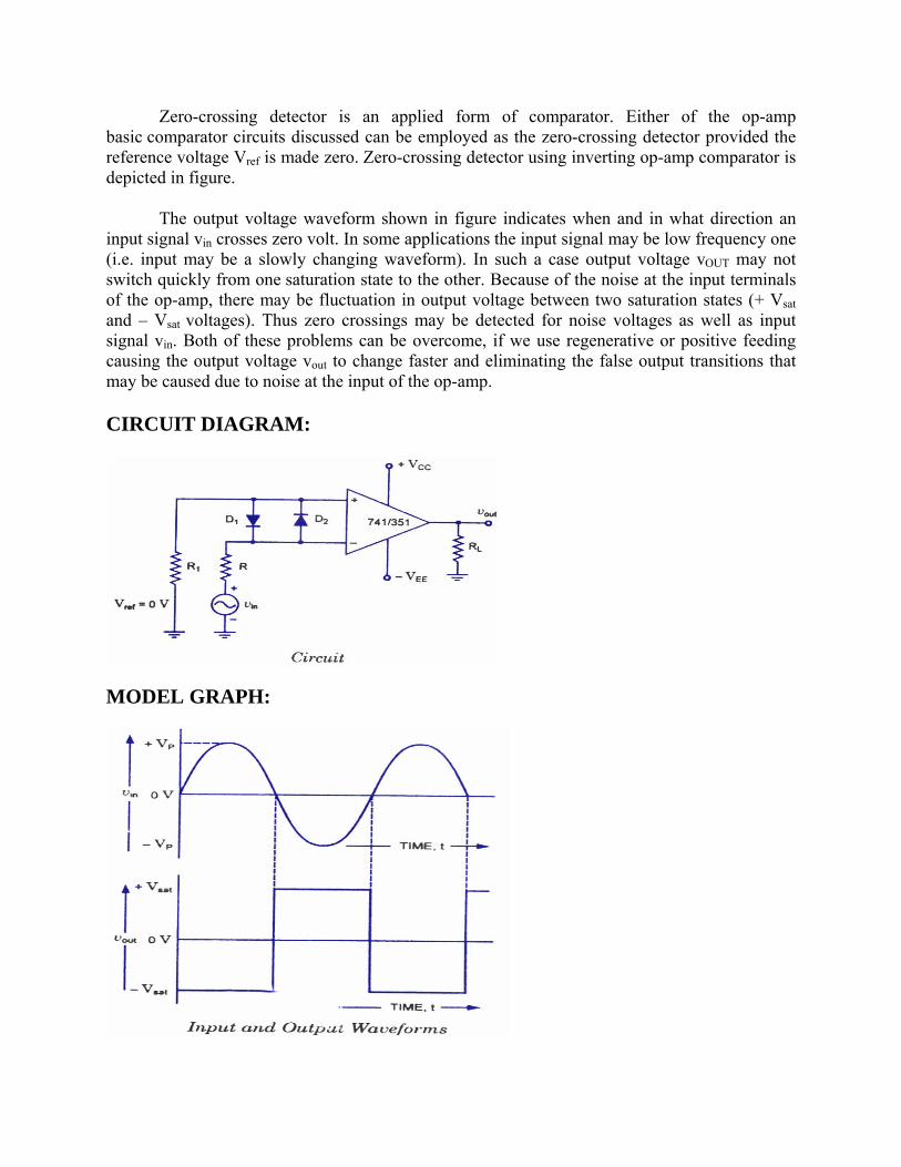
Zero-crossing detector is an applied form of comparator. Either of the op-amp basic comparator circuits discussed can be employed as the zero-crossing detector provided the reference voltage Vref is made zero. Zero-crossing detector using inverting op-amp comparator is depicted in figure.
The output voltage waveform shown in figure indicates when and in what direction an ses zero volt. In some applications the input signal may be low frequency one
(i.e. input may be a slowly changing waveform). In such a case output voltage vOUT may not ate to the other. Because of the noise at the input terminals
of the op-amp, there may be fluctuation in output voltage between two saturation states (+ Vsat and – V
of the op-amp.
CIRC
input signal vin cros
switch quickly from one saturation st
sat voltages). Thus zero crossings may be detected for noise voltages as well as input signal vin. Both of these problems can be overcome, if we use regenerative or positive feeding causing the output voltage vout to change faster and eliminating the false output transitions that may be caused due to noise at the input
1. Connect the circuit as shown in the figure 2. Set the input voltage using AFO to 100mv 3. Observe the output waveform in CRO and measure the output parameter
ESULT:
Thus the characteristics of Non linear OP Amp circuit comparator and Zero crossing etector is verified.
R
d
Post Lab Questions:
. What is a Zero-crossing detector?
. What is a window detector?
. Draw the characteristics of an ideal comparator and that of a commercially available omparator
erm hysteresis
1
2
3c
4. Define the t
RC PHASE SHIFT OSCILLATOR AND WEIN BRIDGE OSCILLATOR
re-Lab questions:P
1. Define Barkhausen criterion for oscillations 2. State the two conditions of oscillations. 3. Classify the Oscillators 4. What is the frequency range of RC phase shift Oscillator 5. Define a wien bridge Oscillator
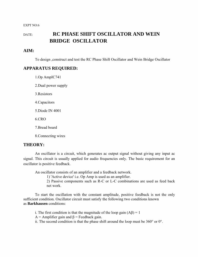
EXPT NO:6
ATE: RC PHASE SHIFT OSCILLATOR AND WEIN BRIDGE OSCILLATOR
To design ,construct and test the RC Phase Shift Oscillator and Wein Bridge Oscillator
1.Op AmpIC741
2.Dual power supply
3.Resistors
pacitors
6.CRO
circuit, which generates ac output signal without giving any input ac signal. applied for audio frequencies only. The basic requirement for an oscillato
plifier and a feedback network. tive device' i.e. Op Amp is used as an amplifier.
ponents such as R-C or L-C combinations are used as feed back
the oscillation with the constant amplitude, positive feedback is not the only
sufficient condition. Oscillator circuit must satisfy the following two conditions known as Bark ons:
is that the magnitude of the loop gain (Aβ) = 1 plifier gain and β = Feedback gain.
second condition is that the phase shift around the loop must be 360° or 0°.
D
AIM:
APPARATUS REQUIRED:
4.Ca
5.Diode IN 4001
7.Bread board
8.Connecting wires
THEORY:
An oscillator is aThis circuit is usuallyr is positive feedback.
An oscillator consists of an am1) 'Ac2) Passive comnet work.
To start
hausen conditi i. The first conditionA = Amii. The
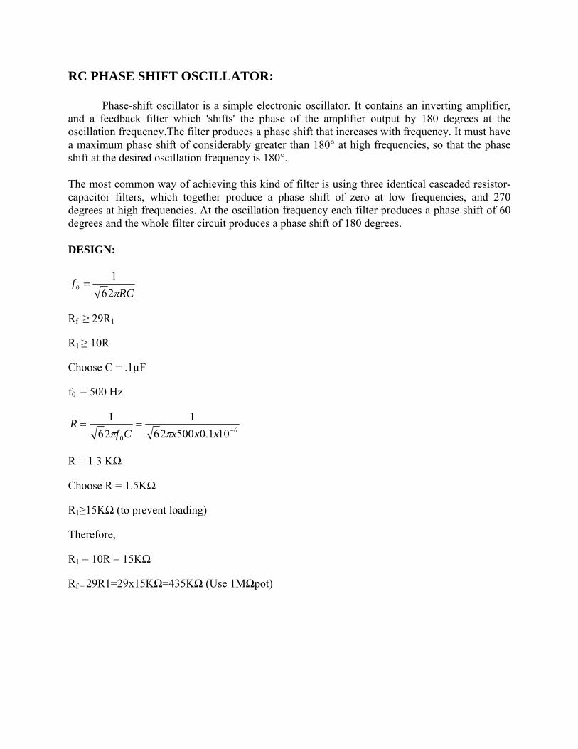
RC PHASE SHIFT OSCILLATOR:
Phase-shift oscillator is a simple electronic oscillator. It contains an inverting amplifier, and a feedback filter which 'shifts' the phase of the amplifier output by 180 degrees at the oscillat ith frequency. It must have a maximum ph quencies, so that the phase shift at the des
The mo t common way of achieving this kind of filter is using three identical cascaded resistor-capacit
ift of 60 circuit produces a phase shift of 180 degrees.
DESIG
ion frequency.The filter produces a phase shift that increases wase shift of considerably greater than 180° at high fre
ired oscillation frequency is 180°.
sor filters, which together produce a phase shift of zero at low frequencies, and 270
degrees at high frequencies. At the oscillation frequency each filter produces a phase shdegrees and the whole filter
N:
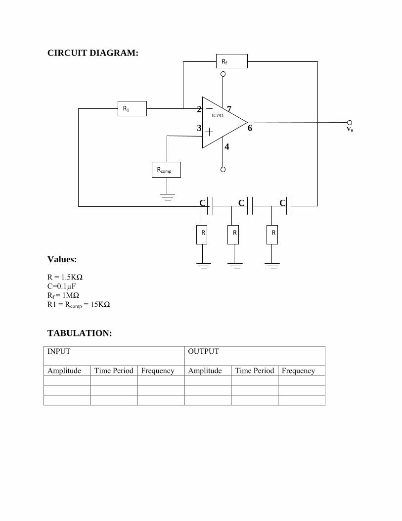
RCf
π261
0 =
R1 ≥ 10R
Rf ≥ 29R1
Choose C = .1µF
f0 = 500 Hz
60 101.05002626 −xxxCf ππ
R = 1.3 KΩ
11==R
Choose R = 1.5KΩ
R1≥15KΩ (to prevent loading)
Therefore,
Ω
Ω=435KΩ (Use 1MΩpot)
R1 = 10R = 15K
Rf = 29R1=29x15K
CIRCUIT DIAGRAM:
2 7
3 6 V0
4
C C C
alues:
= 1.5KΩ =0.1µF
PUT OUTPUT
V
RCRf = 1MΩ R1 = Rcomp = 15KΩ
TABULATION:
IN
Amplitude Time Period Frequency Amplitude Time Period Frequency
IC741
Rf
Rcomp
R1
R R R
MODEEL GRAPHH
Output w
PROCE
RC PHA
1
2
3
WEIN
4
5
Agenerate
Tconnecteadvance 0o.Thenmust ap
p
1
2
3
waveform:
EDURE:
ASE SHIFT
.Design the
.connect th
:
OSCILLA
circuit for f
TOR:
00=500Hz.callculate R1,RR2,and Rf
ee circuit as shhown in the figure with tthe designedd values.
.Switch on tthe power suupply and obbservw the ww
.Note down
.Plot the wav
BRIDGE
A Wien bridga large rang
The Wien Bred with a par
circuit depefor oscillati
ply.:
. With no inp
. The Wien B
. The Voltag
the amplitud
veforms on
OSCILLA
ge oscillator ge of frequen
ridge Oscillrallel RC of
ending uponons to occu
put signal th
Bridge Oscil
ge gain of th
de and time
a graph shee
ATOR
is a type of ncies. The fre
lator uses a f the same c
n the frequenur in a Wien
he Wien Brid
llator can pr
e amplifier m
period.
et.
electronic oequency of o
aveform.
scillator that
feedback ccomponent vncy. At the n Bridge Os
dge Oscillato
roduce a larg
must be at le
oscillation ist generates ssine waves. IIt can
ircuit
s given by:
circuit consiisting of a sseries RC cvalues produucing a phasse delay or pphase resonant freequency ƒr tthe phase shhift is
scillator circcuit the folloowing condiitions
or produces output oscilllations.
ge range of frfrequencies.
east 3.
4. The network can be used with a Non-inverting amplifier.
6. The output resistance of the amplifier must be low so that the effect of external loading is minimised.
e stabilisation in the form of feedback diodes, oscillations from the oscillator can go on indefinitely.
DESIG
5. The input resistance of the amplifier must be high compared to R so that the RC network is not overloaded and alter the required conditions.
7. Some method of stabilizing the amplitude of the oscillations must be provided because if the voltage gain of the amplifier is too small the desired oscillation will decay and stop and if it is too large the output amplitude rises to the value of the supply rails, which saturates the op-amp and causes the output waveform to become distorted.
8. With amplitud
N:
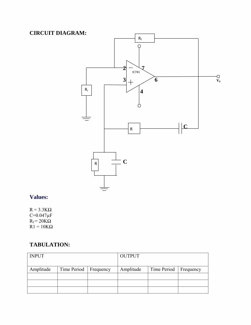
RCf
π20 = 1
3=+ fR 1=V R
Ai
2=i
f
RR
Rf =2Ri
Let c = 0.047µF, f0 = 1KHz
R = Ω= K2.31 Cf2π
0KΩ (use 20K pot)
0
Let Ri = 10KΩ
Rf = 2Ri = 2
CIRCUIT DIAGRAM:
2 7
3 6 V0
4
C
Values:
R = 3.3KΩ
Rf = 20KΩ 1 = 10KΩ
TABULATION:
INPUT OUTPUT
C
C=0.047µF
R
Amplitude Time Period Amplitude Time Period Frequency Frequency
IC741
Rf
R
R
Ri
MODEL GRAPH:
utput waveform:
PROCEDURE:
WEIN BRIDGE OSCILLATOR:
1.Design the circuit for f0=1KHz.calculate R C Rf and Ri
nne s e f e d s.
3.Switch on the power supply and observe the waveform.
amplitude and time period.
5.Plot the waveforms on a graph sheet.
RESU
gned and constru
(i)RC p
(ii) We
O
2.co ct the circuit a shown in th igure with th esigned value
4.Note down the
LT:
Thus the RC Phase Shift oscillator and Wein Bridge oscillator are desicted.
hase shift oscillator F0=
in Bridge oscillator F0=
Post Lab Questions:
1. Explain how the clipping is eliminated in wien bridge oscillator 2. Draw the basic structure of a feedback oscillator. 3. What is the frequency range of LC oscillators 4. For sustained oscillations, what is the gain of the RC phase shift oscillator? 5. Design a phase shift oscillator to oscillate at 100Hz
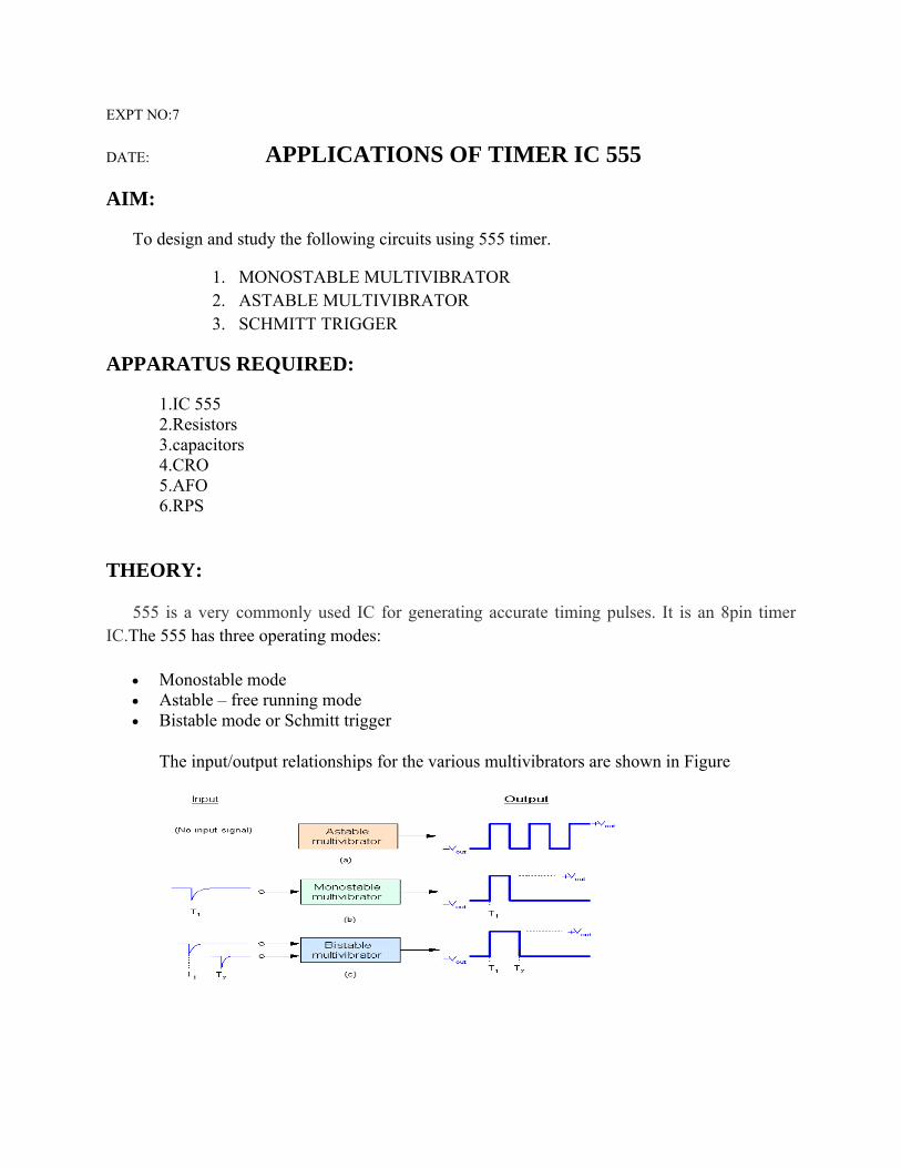
APPLICATIONS OF TIMER IC 555
Pre-Lab questions:
1. Draw the pin diagram of 555 timer IC 2. List the applications of Monostable Multivibrator 3. Define the term Duty cycle 4. For Ra=6.8KΩ,Rb=3.3KΩand C=0.1 μF, Calculate (a)free running frequency (b) Duty
cycle, D 5. Give methods for obtaining symmetrical square wave 6. Why a monostable multivibrator is called a one shot multivibrator 7. Why a Astable multivibrator is called a Free running oscillator
EXPT NO:7
ATE: APPLICATIONS OF TIMER IC 555
To design and study the following circuits using 555 timer.
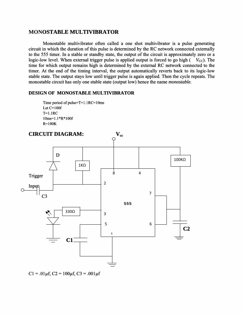
ultivibrator often called a one shot multivibrator is a pulse generating of this pulse is determined by the RC network connected externally
y stat the output of the circuit is approximately zero or a log lo ls is applied output is forced to go high ( VCC). The time for which output remains high is determined by the external RC network connected to the timer. A gic-low stable state. The output stays low until trigger pulse is again applied. Then the cycle repeats. The monostable circuit has only one stable state (output low) hence the name
DESIGN OF MONOSTABLE MULTIVIBRATOR
Time period of pulse=T=1.1RC=10ms Let C=100f T=1.1RC 10ms=1.1*R*100f R=100K
IRCUIT DIAGRAM: Vcc
C2
ONOSTABLE MULTIVIBRATOR OSTABLE MULTIVIBRATOR
Monostable mMonostable mcircuit in which the duratiocircuit in which the duration n to the 555 timer. In a stable or standbto the 555 timer. In a stable or standb e,
ee,eic- w level. When external trigger puic- w level. When external trigger pu
t the end of the timing interval, the output automatically reverts back to its lot the end of the timing interval, the output automatically reverts back to its lo
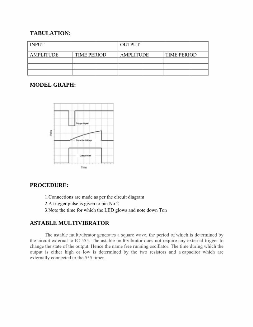
1.Connections are made as per the circuit diagram 2.A supply voltage of 5v to be given 3.The output waveforms at pin3 and pin 2 are observed on a CRO. 4.Measure Ton and toff of the waveform
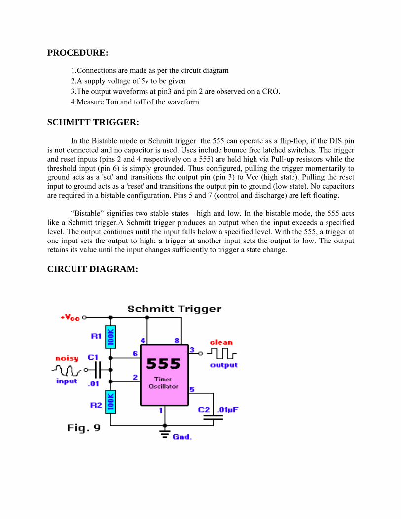
SCHMITT TRIGGER:
In the Bistable mode or Schmitt trigger the 555 can operate as a flip-flop, if the DIS pin is not connected and no capacitor is used. Uses include bounce free latched switches. The trigger and reset inputs (pins 2 and 4 respectively on a 555) are held high via Pull-up resistors while the threshold input (pin 6) is simply grounded. Thus configured, pulling the trigger momentarily to ground acts as a 'set' and transitions the output pin (pin 3) to Vcc (high state). Pulling the reset
in to ground (low state). No capacitors rol and discharge) are left floating.
nifies two stable states—high and low. In the bistable mode, the 555 acts hmitt trigger.A Schmitt trigger p output when the input exceeds a specified
t con put cified 55, a trigger at he ou igge ut set output
tains its value until put c suf ciently to trigger a st .
IRCUIT DIAGRAM:
input to ground acts as a 'reset' and transitions the output pare required in a bistable configuration. Pins 5 and 7 (cont
“Bistable” siglike a Sc roduces an level. The outpuone input sets t
tinues until the intput to high; a tr
falls below a sper at another inp
level. With the 5s the output to low. The
re the in hanges fi ate change
C
TABU
INPUT OUTPUT
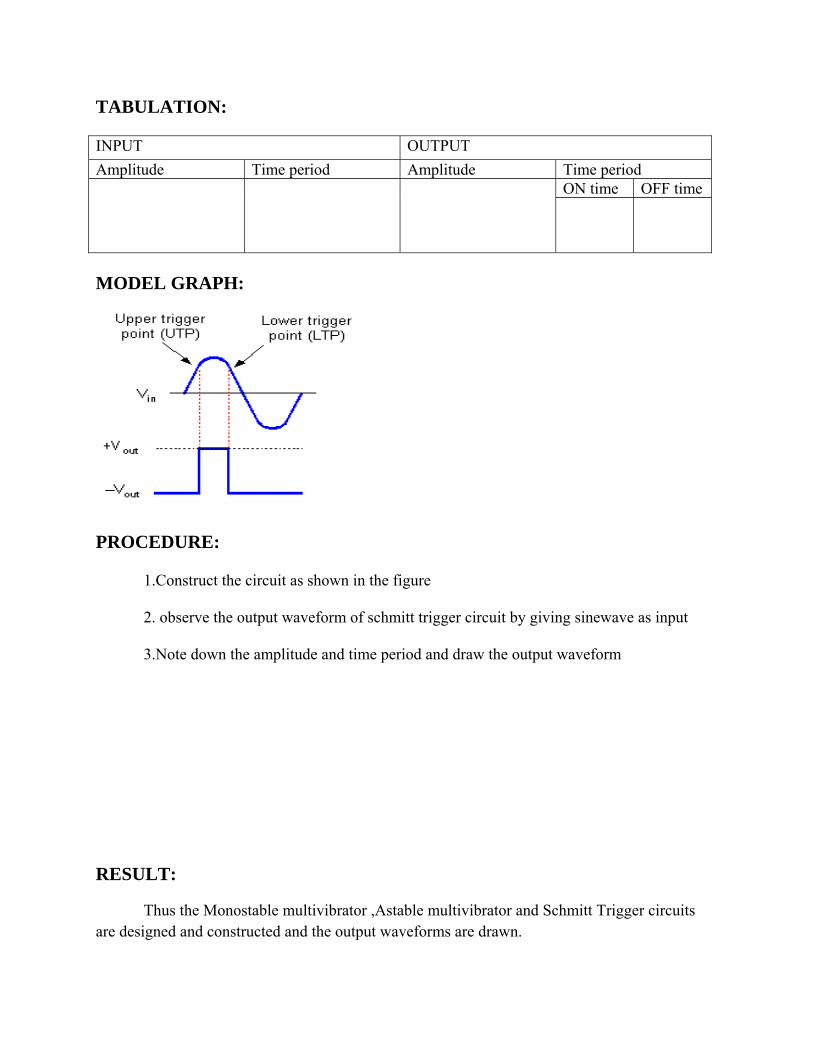
LATION:
Amplitude Time period Amplitude Time period ON time OFF time
MODEL GRAPH:
PROCEDURE:
1.Construct the circuit as shown in the figure
2. observe the output waveform of schmitt trigger circuit by giving sinewave as input
3.Note down the amplitude and time period and draw the output waveform
ESULT:
stable multivibrator ,Astable multivibrator and Schmitt Trigger circuits the output waveforms are drawn.
R
Thus the Monoare designed and constructed and
Post Lab Questions:
1. Discuss the operation of a FSK generator using 555 timer. 2. How is an Astable multivibrator connected into a pulse position modulator. 3. Explain the function of reset?
des of operation of a timer? 5. Derive the expression of time delay of a monostable multivibrator.
4. What are the mo
STUDY OF TIMER IC 555
Pre-Lab questions:
1. Draw the pin diagram of 555 timer IC 2. What are the features of 555 Timer IC 3. Give the applications of Timer IC 555 4. Define Flip flop 5. What is a comparator? what are the applications of comparator
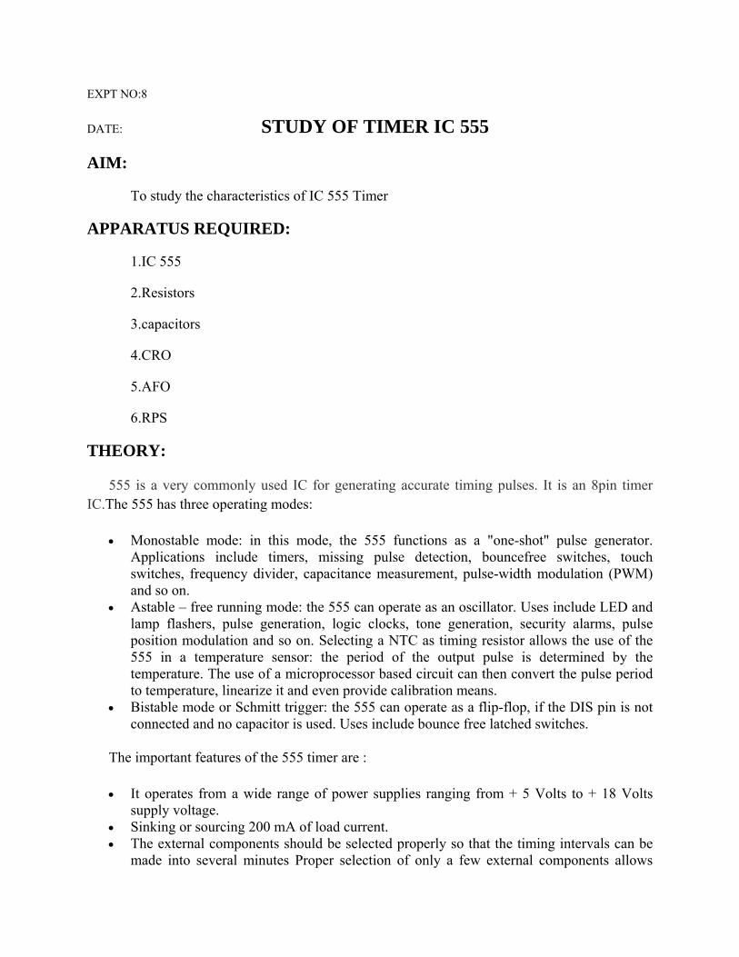
EXPT NO:8
DATE: STUDY OF TIMER IC 555
imer
1.IC 555
2.Resistors
3.capacitors
4.CRO
5.AFO
6.RPS
HEORY:
555 is a very commonly used IC for generating accurate timing pulses. It is an 8pin timer IC.The 555 has three operating modes:
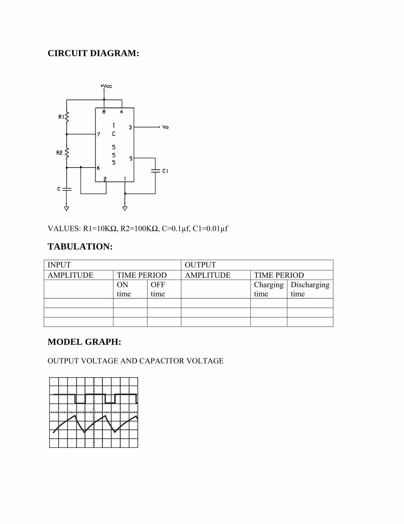
• Monostable mode: in this mode, the 555 functions as a "one-shot" pulse generator. Applications include timers, missing pulse detection, bouncefree switches, touch switches, frequency divider, capacitance measurement, pulse-width modulation (PWM) and so on.
• Astable – free running mode: the 555 can operate as an oscillator. Uses include LED and lamp flashers, pulse generation, logic clocks, tone generation, security alarms, pulse position modulation and so on. Selecting a NTC as timing resistor allows the use of the 555 in a temperature sensor: the period of the output pulse is determined by the temperature. The use of a microprocessor based circuit can then convert the pulse period to temperature, linearize it and even provide calibration means.
• Bistable mode or Schmitt trigger: the 555 can operate as a flip-flop, if the DIS pin is not connected and no capacitor is used. Uses include bounce free latched switches.
The important features of the 555 timer are :
• It operates from a wide range of power supplies ranging from + 5 Volts to + 18 Volts supply voltage.
• Sinking or sourcing 200 mA of load current. external components should be selected properly so that the timing intervals can be
made into several minutes Proper selection of only a few external components allows
AIM:
To study the characteristics of IC 555 T
APPARATUS REQUIRED:
T
• The
tikiming intervaals of severaal minutes allong with thhe frequenciees exceedingg several hunndred
• It• I
ilo hertz.
tt has a high c
te• T
p
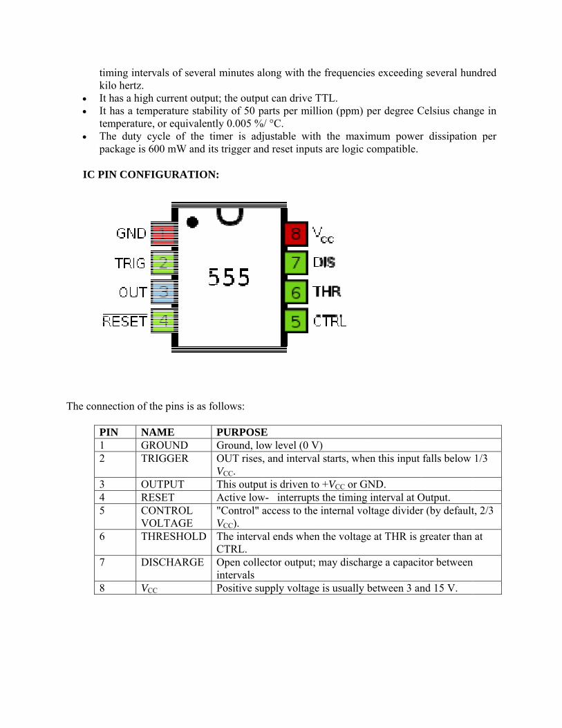
IC PI
The conn
P1 2
3 4 5
6
7
8
t has a tempcurrent outpu
emperature, The duty cy
ackage is 60
IN CONFIG
nection of th
PIN NAMGROTRI
OUTRESCONVOLTHR
DIS
VCC
perature stabut; the outpu
or equivalencle of the t
00 mW and i
GURATION
he pins is as f
ME OUND IGGER
TPUT SET NTROL LTAGE RESHOLD
SCHARGE
ility of 50 put can drive T
ntly 0.005 %timer is adjits trigger an
N:
follows:
PURPOSEGround, loOUT rises,VCC. This outpuActive low"Control" aVCC). The intervaCTRL. Open colleintervals Positive su
parts per milTTL. lion (ppm) pper degree CCelsius channge in
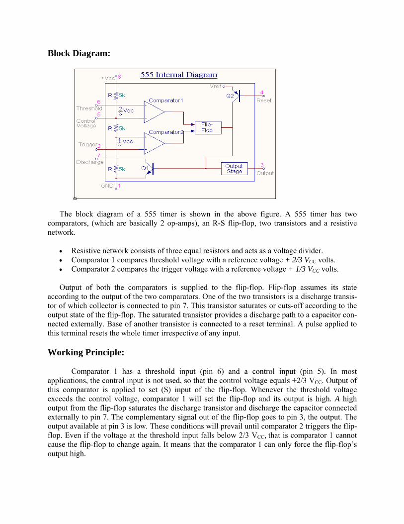
The block diagram of a 555 timer is shown in the above figure. A 555 timer has two comparators, (which are basically 2 op-amps), an R-S flip-flop, two transistors and a resistive network.
• Resistive network consists of three equal resistors and acts as a voltage divider. • Comparator 1 compares threshold voltage with a reference voltage + 2/3 VCC volts. • Comparator 2 compares the trigger voltage with a reference voltage + 1/3 VCC volts.
supplied to the flip-flop. Flip-flop assumes its state rators. One of the two transistors is a discharge transis-
tor of which transistor saturates or cuts-off according to the output f th The s es a discharge path to a capacitor con-nected ternally othethis ter al rese time
Work g Prin
mpara thrapplications, the control input is not used, this co arator e e exceeds high output from the es cted externally to pin 7. The complemoutput available at pin 3 is low. T he flip-
f the voltage at the threshold input falls below 2/3 VCC, that is comparator 1 cannot ause the flip-flop to change again. It means that the comparator 1 can only force the flip-flop’s
output high.
Diagram:
Output of both the comparators is according to the output of the two compa
collectostate o
r is connectede flip-flo
to pin 7. Thisaturated transp.
. Base of anistor provid
r transistor is connected tex o a reset terminal. A pulse applied to r irrespective of any input. min ts the whole
in ciple:
Co tor 1 has a eshold input (pin 6) and a control input (pin 5). In most so that the control voltage equals +2/3 VCC. Output of
t (S) input of the flip-flop. Whenever the threshold voltagparator
mp is applied to s the control voltage, com
flip-flop saturat1 will set the flip-flop and its output is high. A
the discharge transistor and discharge the capacitor conneentary signal out of the flip-flop goes to pin 3, the output. The hese conditions will prevail until comparator 2 triggers t
flop. Even ic
To change the output of flip-flop to low, the voltage at the trigger input must fall below + 1/3 Vcc. When this occurs, comparator 2 triggers the flip-flop, forcing its output low. The low output from the flip-flop turns the discharge transistor off and forces the power amplifier to output a high. These conditions will continue independent of the voltage on the trigger input. Comparator 2 can only cause the flip-flop to output low.From the above discussion it is concluded that for the having low output from the timer 555, the voltage on the threshold input must exceed the control voltage or + 2/3 VCC. They also turn the discharge transistor on. To force the output from the timer high, the voltage on the trigger input must drop below +1/3 VCC. This also turns the discharge transistor off.
A voltage may be applied to the control input to change the levels at which the switching occurs. When not in use, a 0.01 nano Farad capacitor should be connected between pin 5 and ground to prevent noise coupled onto this pin from causing false triggering.Connecting the reset (pin 4) to a logic low will place a high on the output of flip-flop. The discharge transistor will go on and the power amplifier will output a low. This condition will continue until reset is taken high. This allows synchronization or resetting of the circuit’s operation. When not in use, reset should be tied to +VCC.
the functions of IC 555 Timer is studied
RESULT:
Thus
Post Lab Questions:
1. Discuss the operation of a FSK generator using 555 timer. 2. How is an Astable multivibrator connected into a pulse position modulator. 3. Explain the function of reset? 4. What are the modes of operation of a timer? 5. Derive the expression of time delay of a monostable multivibrator.
STUDY OF FUNCTION GENERATOR IC566
re-Lab questions:P
566. to generate by using a function generator.
4. What are the conditions of a self-sustained oscillation? 5. List some applications of Function Generator.
1. Draw the pin diagram of NE/SE2. What are the types of waveforms that are able3. Draw the transfer characteristics of sine shaper circuit.
EXPT NO:9
OF FUNCTION GENERATOR IC566
IM:
lled oscillator IC 566 and to generate the square
1.IC 566
2.Resistors
3.capacitors
4.Regulated power Supply
5.Cathode Ray Oscilloscope
EORY:
A Voltage-Controlled Oscillator (VCO) is a circuit that provides a varying output signal ypically of square-wave or triangular-wave form) whose frequency can be adjusted over a
ange controlled by a dc voltage. An example of a VCO is the 566 IC unit, which contains wave and triangular-wave signals whose frequency is set by an
xternal resistor and capacitor and then varied by an applied dc voltage.
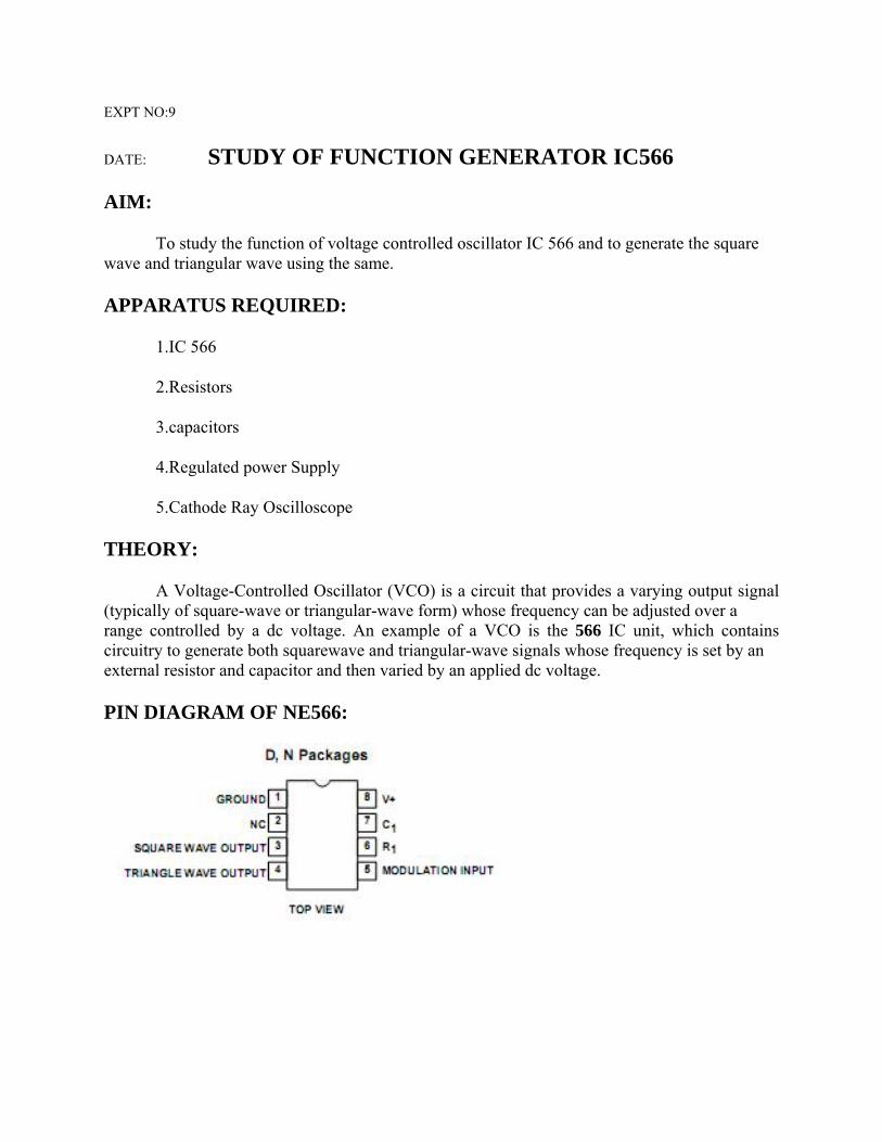
IN DIAGRAM OF NE566:
DATE: STUDY
A
To study the function of voltage controwave and triangular wave using the same.
APPARATUS REQUIRED:
TH
(trcircuitry to generate both squaree
P
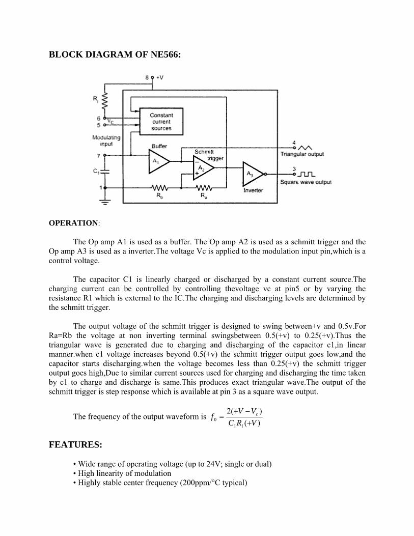
BLOCK DIAGRAM OF NE566:
OPER
buffer. The Op amp A2 is used as a schmitt trigger and the .The voltage Vc is applied to the modulation input pin,which is a
.
the
The output voltage of the schmitt trigger is designed to swing between+v and 0.5v.For ng terminal swingsbetween 0.5(+v) to 0.25(+v).Thus the
triangular wave is generated due to charging and discharging of the capacitor c1,in linear manner.when c1 voltage increases beyond 0.5(+v) the schmitt trigger output goes low,and the capacitor starts discharging.when the voltage becomes less than 0.25(+v) the schmitt trigger output goes high,Due to similar current sources used for charging and discharging the time taken by c1 to charge and discharge is same.This produces exact triangular wave.The output of the schmitt trigger is step response which is available at pin 3 as a square wave output.
The frequency of the output waveform is
ATION:
The Op amp A1 is used as a Op amp A3 is used as a invertercontrol voltage
The capacitor C1 is linearly charged or discharged by a constant current source.The charging current can be controlled by controlling thevoltage vc at pin5 or by varyingresistance R1 which is external to the IC.The charging and discharging levels are determined by the schmitt trigger.
Ra=Rb the voltage at non inverti
)()(2
110 VRC
VVf c
+−+
=
EATURES:
• Wide range of operating voltage (up to 24V; single or dual) • High linearity of modulation • Highly stable center frequency (200ppm/°C typical)
F
• Highly linear triangle wave output • Frequency programming by means of a resistor or capacitovoltage or current • Frequency adjustable over 10-to-1 range with same
APPLICATIONS:
• Tone generators • Frequency shift keying • FM modulators • Clock generators • Signal generators
r,
capacitor
• Function generators
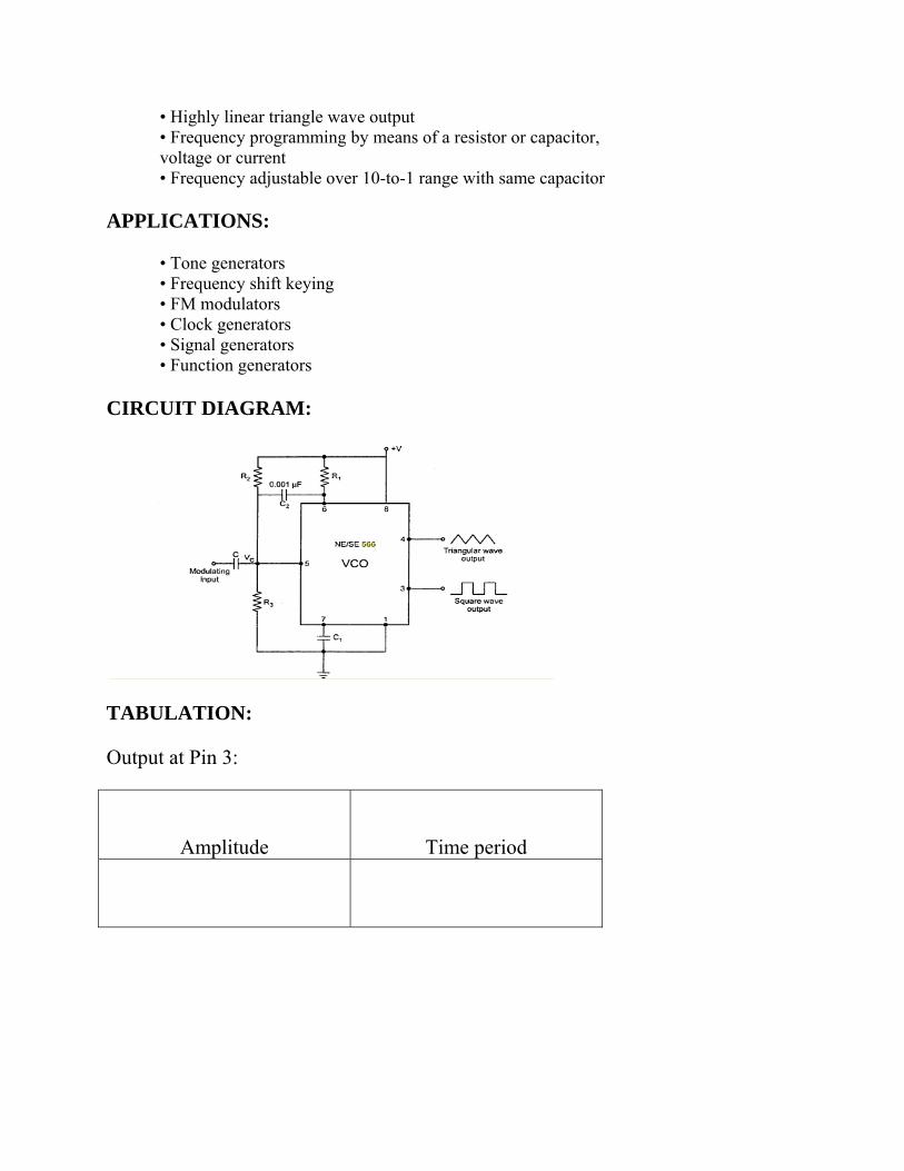
CIRCUIT DIAGRAM:
TABULATION:
Output at Pin 3:
Amplitude
Time period
Outpu
Amcapacitor of capacitor
t at Pin 4:
plitude Charging time of Discharging time
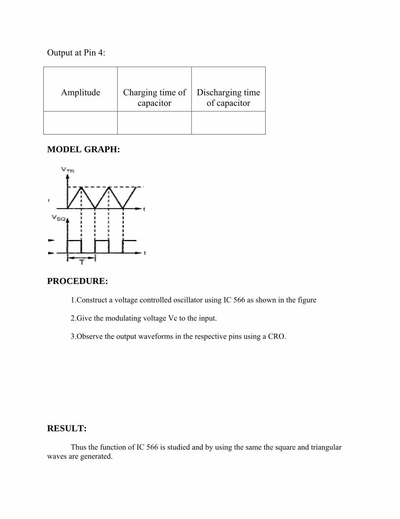
MOD
PROCEDURE:
1.Construct a voltage controlled oscillator using IC 566 as shown in the figure
ge Vc to the input.
3.Observe the output waveforms in the respective pins using a CRO.
Thus the function of IC 566 is studied and by using the same the square and triangular aves are generated.
EL GRAPH:
2.Give the modulating volta
RESULT:
w
Post Lab Questions:
1. Wh C that can be sed to build a function generator. 2. Draw the pin configuration of XR-2206 monolithic IC.
term 4. lock d o5. What is the purpose of using Constant current source in NE 566.