Web site - http://www.semiconductors.philips.com is replaced with http://www.stnwireless.com
Contact information - the list of sales offices previously obtained by sending an email to [email protected], is now found at http://www.stnwireless.com under Contacts.
If you have any questions related to the document, please contact our nearest sales office.Thank you for your cooperation and understanding.
ST-NXP Wireless
www.stnwireless.com
1. General description
The TEA5764UK is a single chip electronically tuned FM stereo radio with Radio DataSystem (RDS) and Radio Broadcast Data System (RBDS) demodulator and RDS/RBDSdecoder for portable application with fully integrated IF selectivity and demodulation.
The radio is completely adjustment free and only requires a minimum of small and lowcost external components.
The radio can tune to the European, US and Japanese FM bands. It has a low powerconsumption and can operate at a low supply voltage.
2. Features
Chip scale package
High sensitivity due to integrated low noise RF input amplifier
FM mixer for conversion of the US/Europe (87.5 MHz to 108 MHz) and Japanese FMband (76 MHz to 90 MHz) to IF
Preset tuning to receive Japanese TV audio up to 108 MHz
Auto search tuning, raster 100 kHz
RF automatic gain control circuit
LC tuner oscillator operating with low cost fixed chip inductors
Fully integrated FM IF selectivity
Fully integrated FM demodulator; no external discriminator
Crystal oscillator at 32768 Hz, or external reference frequency at 32768 Hz
PLL synthesizer tuning system
IF counter; 7-bit output via the I2C-bus
Level detector; 4-bit level information output via the I2C-bus
Soft mute: signal dependent mute function
Mono/stereo blend: gradual change from mono to stereo, depending on signal
Adjustment-free stereo decoder
Autonomous search tuning function
Standby mode
MPX output
One software programmable port
Fully integrated RDS/RBDS demodulator in accordance with EN50067
RDS/RBDS decoder with memory for two RDS data blocks provides blocksynchronization and error correction; block data and status information are availablevia the I2C-bus
Audio pause detector
TEA5764UKFM radio + RDSRev. 02 — 9 August 2005 Product data sheet
Philips Semiconductors TEA5764UKFM radio + RDS
Interrupt flag
3. Applications
FM stereo radio
4. Quick reference data
Table 1: Electrical parameters generalThe listed parameters are valid when a crystal is used that meets the requirements as stated in Table 46; All RF input valuesare defined in potential difference, except when EMF is explicitly stated.
Symbol Parameter Conditions Min Typ Max Unit
Supplies
VCCA analog supply voltage 2.5 2.7 3.3 V
ICCA analog supply current VCCA = 2.5 V to 3.3 V
operating mode 12 13.7 16 mA
Standby mode 0 0.1 1 µA
VCCD digital supply voltage 2.5 2.7 3.3 V
ICCD digital supply current VCCD = 2.5 V to 3.3 V
operating mode 0.3 0.7 1.5 mA
Standby mode 1 15 22.5 µA
Reference voltage
VVREFDIG digital reference voltagefor I2C-bus interface
Table 1: Electrical parameters generalThe listed parameters are valid when a crystal is used that meets the requirements as stated in Table 46; All RF input valuesare defined in potential difference, except when EMF is explicitly stated.
Product data sheet Rev. 02 — 9 August 2005 5 of 64
Philips Semiconductors TEA5764UKFM radio + RDS
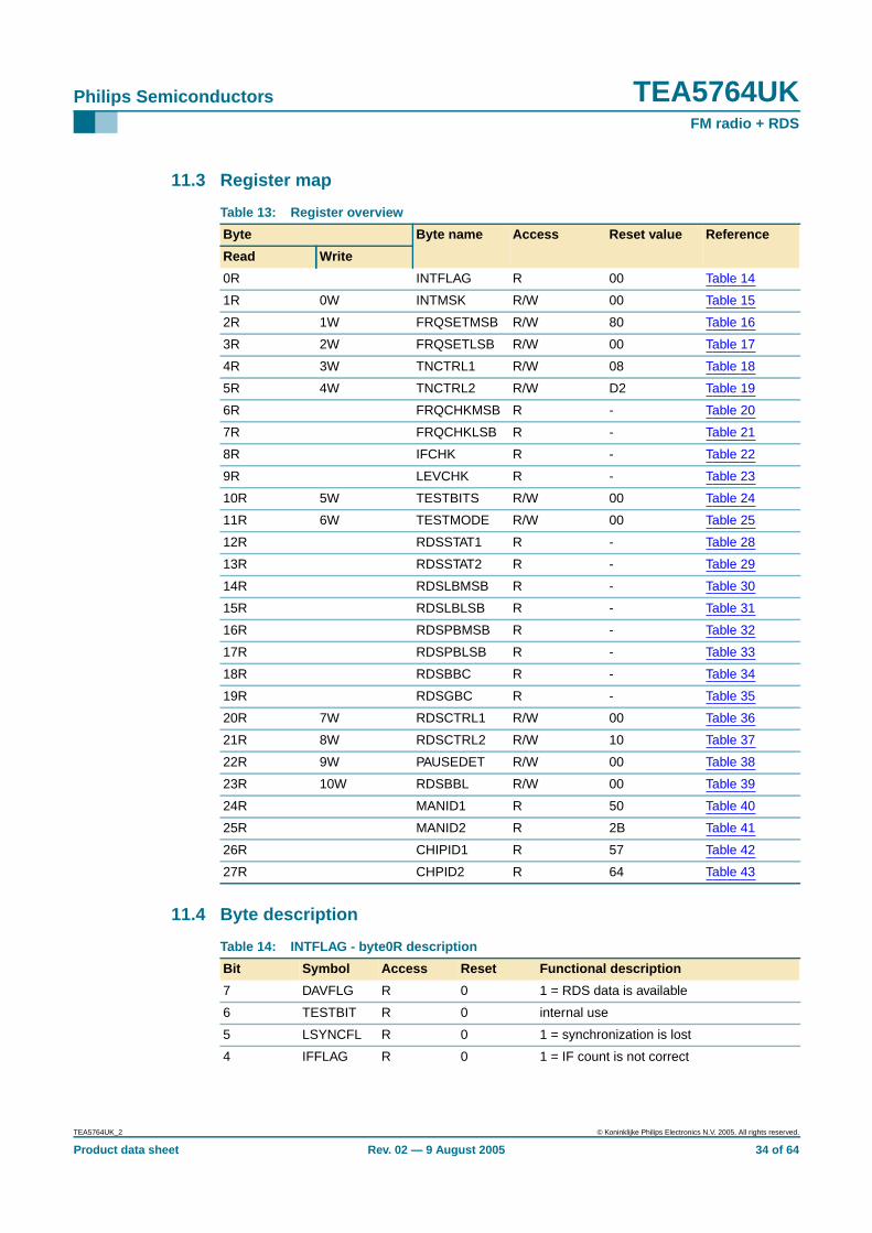
8. Functional description
8.1 Low noise RF amplifierThe LNA input impedance together with the LC RF input circuit defines an FM band filter.The gain of the LNA is controlled by the RF AGC circuit.
8.2 FM I/Q mixerFM quadrature mixer converts FM RF (76 MHz to 108 MHz) to IF.
8.3 VCOThe varactor tuned LC VCO provides the Local Oscillator (LO) signal for the FMquadrature mixer. The VCO frequency range is 150 MHz to 217 MHz.
8.4 Crystal oscillatorThe crystal oscillator can operate with a 32.768 kHz clock crystal. The oscillator can beoverridden via the FREFIN pin. When the FREFIN pin is used the oscillator is clockedexternally by a 32.768 kHz signal. Selection between a reference clock or a referencecrystal can be done via the I2C-bus. When a crystal is connected the FREFIN pin must beleft open-circuit, and when pin FREFIN is used a crystal may not be connected. It is notpossible to connect a crystal and apply a frequency via the FREFIN pin in the sameapplication.
TMUTE G6 soft mute time-constant capacitor
VAFR G5 right audio output
VAFL F4 left audio output
MPXOUT G4 FM demodulator MPX output
MPXIN G3 MPX decoder and RDS decoder MPX input
GNDD G2 digital ground; this pin has an internal pull-down resistor of 10 kΩto ground
Product data sheet Rev. 02 — 9 August 2005 6 of 64
Philips Semiconductors TEA5764UKFM radio + RDS
The crystal oscillator generates the reference frequency for the following:
• Reference frequency divider for synthesizer PLL
• Timing for the IF counter
• Timing for the pause detector
• Free running frequency adjustment of the stereo decoder VCO
• Centre frequency for adjustment of the IF filters
• Clock frequency of the RDS/RBDS decoder
8.5 PLL tuning systemThe PLL synthesizer tuning system is suitable to operate with a 32.768 kHz referencefrequency generated by the crystal oscillator or a reference clock of 32.768 kHz fed intothe TEA5764UK. To tune the radio to the required frequency requires the PLL word to becalculated and then programmed to the register. The PLL word is 14 bits long; seeTable 20 and Table 21. Calculation of this 14-bit word can be done as follows.
Formula for high-side injection:
(1)
Formula for low-side injection:
(2)
where:
NDEC = decimal value of PLL word
fRF = wanted tuning frequency (Hz)
fIF = intermediate frequency of 225 kHz
fREFS = the reference frequency of 32.768 kHz
Example for receiving a channel at 100.1 MHz:
(3)
The result found using Equation 1 or Equation 2 must always be rounded to the lowestinteger value. If rounded down to the lowest integer value of NDEC = 12246, the PLL wordbecomes 2FD6h.
This value can be written to register FRQSETLSB or FRQSETMSB via the I2C-bus andthe IC will then either start an autonomous search at this frequency or go to a presetchannel at this frequency. When the application is built according to the block diagramshown in Figure 1, and with the preferred components, the PLL will settle to the newfrequency within 5 ms. The most accurate tuning is accomplished when a search isfollowed by a preset to the same frequency.
Product data sheet Rev. 02 — 9 August 2005 7 of 64
Philips Semiconductors TEA5764UKFM radio + RDS
The PLL is triggered by writing to any one of the bytes FRQSETMSB, FRQSETLSB,TNCTRL1, TNCTRL2, TESTBITS, TESTMODE.
Accurate validation of the PLL locking on the new frequency can take 2 ms to 10 ms.When a lock is detected, bit LD is set.
8.6 Band limitsThe TEA5764UK can be switched either to the Japanese FM band or to the US/EuropeFM band. Setting bit BLIM to logic 0 the band range is 87.5 MHz to 108 MHz; setting bitBLIM to logic 1 selects the Japanese band range of 76 MHz to 90 MHz.
8.7 RF AGCThe RF AGC (or wideband AGC) prevents overloading and limits the amount ofintermodulation products created by strong adjacent channels. The RF AGC is on bydefault and can be turned off via the I2C-bus.
The TEA5764UK also has an in-band AGC to prevent overloading by the wanted channel.The in-band AGC is always turned on.
8.8 Local or long distance receiveIf bit LDX = 1, the LNA gain is reduced by 6 dB to prevent distortion when a transmitter isvery near. If bit LDX = 0, the LNA gain is normal to receive long distance (DX) stations.
8.9 IF filterA fully integrated IF filter is built-in.
8.10 FM demodulatorThe FM quadrature demodulator has an integrated resonator to perform the phase shift ofthe IF signal.
8.11 IF counterThe received signal is mixed to produce an IF of 225 kHz. The result of the mixing iscounted. A good IF count result indicates that the radio is tuned to a valid channel insteadof an image or a channel with much interference. The IF counter outputs a 7-bit countresult via the I2C-bus. The IF counter is continuously active and can be read at any timevia the I2C-bus. It also activates a flag when the IF count result is outside the IF countvalid result window; see Section 9.1.4.4.
Before a tuning cycle is initiated the IF count period can be set to 2 ms or to 15.6 ms bybit IFCTC. When the IF count period is set to 2 ms, initiating the tuning algorithm with apreset (bit SM = 0) will always give an RDS update as shown in Section 8.22.1. In casethe IF count time is set to 15.6 ms, the tuning flowchart illustrated in Figure 3 is used.Once tuned, the IF count period is always 15.6 ms.
Product data sheet Rev. 02 — 9 August 2005 8 of 64
Philips Semiconductors TEA5764UKFM radio + RDS
8.12 Voltage level generator and analog-to-digital converterThe voltage level indicates the field strength received by the antenna. The voltage level isanalog-to-digital converted to a 4-bit word and output via the I2C-bus. The ADC level iscontinuously active and can be read at any time via the I2C-bus. It also activates a flagwhen the voltage level falls below a predefined selectable threshold. Bit LHSW allowseither large or small hysteresis steps to be chosen; see Table 24 and Section 9.1.4.5.
When the ADC level is set to 3, its minimum value, the search algorithm will only stop atchannels having a RF level higher than, or equal to, ADC level 3. After completing thesearch algorithm and being tuned to a station, due to hysteresis the effective limit will beset to 0. This means that the continuous ADC level check will never set the LEVFLAG.
8.13 Mute
8.13.1 Soft mute
The low-pass filtered voltage level drives the soft mute attenuator at low RF input levels:the audio output is faded and hence also the noise (see graphs referenced 1 in Figure 15and Figure 17).
The soft mute function can also be switched off via the I2C-bus, using bit SMUTE.
8.13.2 Hard mute
The audio outputs VAFL and VAFR can be hard-muted by bit MU in byte TNCTRL2, whichmeans that they are put into 3-state. This can also be done by setting bits Left Hard Mute(LHM) or Right Hard Mute (RHM) in byte TESTBITS, which allows either one or bothchannels to be muted and forces the TEA5764UK to mono mode. When the TEA5764UKis in Standby mode the audio outputs are hard-muted.
8.13.3 Audio frequency mute
The audio signal is muted by setting bit AFM of the TNCTRL1 register to logic 1. In thesoft mute attenuator the audio signal is blocked and so pins VAFL and VAFR will be attheir DC biasing point with no signal.
The audio is automatically muted during an RDS update as shown in the flowchart ofFigure 3. When the audio must be muted during Search mode, it is done by setting bitAFM to logic 1 before the search action and resetting it to logic 0 afterwards.
Setting bit AFM to logic 0 stops the RDS data.
8.14 MPX decoderThe PLL stereo decoder is adjustment free. It can be switched to mono via the I2C-bus.
8.15 Signal dependent mono/stereo blend (stereo noise cancellation)If the RF input level decreases, the MPX decoder blends from stereo to mono to limit theoutput noise. The continuous mono-to-stereo blend can also be programmed via theI2C-bus to an RF level dependent switched mono-to-stereo transition. Stereo noisecancellation can be switched off via the I2C-bus by bit SNC.
Product data sheet Rev. 02 — 9 August 2005 9 of 64
Philips Semiconductors TEA5764UKFM radio + RDS
8.16 Software programmable portOne software programmable port (CMOS output) can be addressed via the I2C-bus:
Bit SWPM = 1, the software port functions as the output for the FRRFLAG.
Bit SWPM = 0, the software port outputs bit SWP of the registers.
In Test mode the software port outputs signals according to Table 27. Test mode isselected, setting bit TM of byte TESTMODE to logic 1.
The software port cannot be disabled by the PUPD bits; see Section 8.17.
8.17 Standby modeThe radio can be put into Standby mode by the Power-Up / Power-Down (PUPD) bits. TheRDS part can be turned off separately or both the RDS and the FM part can be turned off.The TEA5764UK is still accessible via the I2C-bus but takes only a low power from thesupply, in Standby mode, the audio outputs are hard-muted.
8.18 Power-on resetAfter startup of VCCA and VCCD a power-on reset circuit will generate a reset pulse and theregisters will be set to their default values. The power-on reset is effectively generated byVCCD.
After a power-on reset the TEA5764UK is in Standby mode and the PUPD bits are set tologic 0. After a power-on reset the registers are reset to their default value, except forbyte12R to byte19R and flags DAVFLG, LSYNCFLG and PDFLAG. To reset these, theRDS part must be turned on by setting PUPD. After setting PUPD to logic 1, it will take0.9 ms to start-up the TEA5764UK and set these registers to their default value.
The power supplies can be switched on in any order.
When the supply voltage VCCA and VCCD are at 0 V, all I/Os, the audio outputs and thereference clock input are high-ohmic.
8.19 RDS/RBDS
8.19.1 RDS/RBDS demodulator
A fully integrated RDS/RBDS demodulator which uses the reference frequency(32.678 Hz) of the PLL synthesizer tuning system. The RDS demodulator recovers andregenerates the continuously transmitted RDS or RBDS data stream of the multiplexsignal (MPXRDS) and provides the signals clock (RDCL), data (RDDA) for furtherprocessing by the integrated RDS decoder.
8.19.2 RDS data and clock direct
The RDS demodulator retrieves the RDS data and clock signals, this data can be putdirectly onto pins VAFL and VAFR by setting bit RDSCDA to logic 1.
Product data sheet Rev. 02 — 9 August 2005 10 of 64
Philips Semiconductors TEA5764UKFM radio + RDS
8.19.2.1 RDS/RBDS decoder
The RDS decoder provides block synchronization, error correction and flywheel functionfor reliable extraction of RDS or RBDS block data. Different modes of operation can beselected to fit different application requirements. Availability of new data is signalled by bitDAVFLG and output pin INTX which generates an interrupt. Up to two blocks of data andstatus information are available via the I2C-bus in a single transmission.
The behavior of the DAVFLG is described in Section 10.
8.20 Audio pause detectorThe audio pause detector monitors the audio modulation for pauses and responds to lowlevels. The modulation threshold can be adjusted in 4 steps of 4 dB by control bits PL[1:0].The minimum time for detecting a pause can be adjusted by control bits PT[1:0] as shownin Table 38. When a pause occurs, flag PDFLAG is set to logic 1 and a hardware interruptis generated; see Section 9.1.4.6.
8.21 Auto search and Preset modeIn Search mode the TEA5764UK can search channels automatically (see Figure 3).
Product data sheet Rev. 02 — 9 August 2005 11 of 64
Philips Semiconductors TEA5764UKFM radio + RDS
Before starting a search or a preset, the INTMSK register must be reset and only theFRRMSK must be set. This allows the microprocessor to be interrupted only when thesearch or preset algorithm is ready.
Fig 3. Flowchart auto search or preset
001aab461
during a preset mute is always activesearch mode is default not muted
Product data sheet Rev. 02 — 9 August 2005 12 of 64
Philips Semiconductors TEA5764UKFM radio + RDS
8.21.1 Search mode
Search mode is initiated by setting bit SM in byte FRQSETMSB to logic 1. The searchdirection is set by bit SUD; SUD = 0 (search down), bit SUD = 1 (search up). The tunerstarts searching at the frequency set in bytes FRQSETLSB and FRQSETMSB. TheSearch Stop Level (SSL) bits define the field strength level at which a desired channel isdetected. The tuner will stop on a channel with a field strength equal to or higher than thisreference level and then checks the IF frequency; when both are valid, the search stops(Note that this depends on bit AHLSI described in Figure 3). If the level check or theIF-count fails, the search continues. If no channels are found, the TEA5764UK stopssearching when it has reached the band limit, setting the BLFLAG HIGH. A search alwaysstops when the FRRFLAG is set and on the occurrence of a hardware interrupt, thisprocedure is shown in Figure 3.
The search algorithm can stop at a frequency that is offset from the IF by up to amaximum of 12 kHz. The maximum offset can be limited to 8 kHz by applying a preset.For optimum tuning, it is recommended that a preset is applied after a search and whenthe found frequency has an offset that is above 8 kHz.
After this interrupt the TEA5764UK will not update the tuner registers for a period of 15ms. The state of the TEA5764UK can be checked by reading the bytes of INTFLAG,FRQCHKMSB, FRQCHKLSB, TNCTRL1 and TNCTRL2. Table 4 shows the possiblestates of these registers after an auto search.
[1] This table is valid until 30.6 ms after the tuning cycle has completed. It shows the outcome of the flagregister when a read is done after pin INTX goes LOW on condition that no mask bit other than FRRMSK isset.
8.21.2 Preset mode
A preset occurs by setting bit SM to logic 0 and writing a frequency to byte FRQSETMSB.The tuner jumps to the selected frequency and sets the FRRFLAG when it is ready.
After this interrupt the TEA5764UK will not update the tuner registers for a period of15 ms. The state of the TEA5764UK can be checked by reading registers: INTFLAG,FRQCHKLSB, FRQCHKMSB, TNCTRL1 and TNCTRL2. Table 4 shows the possiblestates after a preset.
Table 4: Tuner truth table [1]
IFFLAG BLFLAG FRRFLAG Comment
0 0 0 if pin INTX has gone LOW and only IFMSK, FRRMSK andBLMSK were set then this cannot occur
0 0 1 channel found during search / preset; FRRMSK set
0 1 0 not a valid state
0 1 1 a valid channel found and the band limit has been reachedduring a search; BLMSK or FRRMSK set
1 0 0 not a valid state
1 0 1 a preset or search has occurred but the wanted channel has avalid RSSI level but fails the IF count when AHLSI was set tologic 1; HLSI must be toggled and a new PLL value must beprogrammed; FRRMSK set
1 1 0 not a valid state
1 1 1 band limit is reached during search; no valid channel found;BLMSK or FRRMSK set
Product data sheet Rev. 02 — 9 August 2005 13 of 64
Philips Semiconductors TEA5764UKFM radio + RDS
8.21.3 Auto high-side and low-side injection stop switch
When a channel is searched or a preset is done, reception can sometimes improve wheninjection is done at the other side of the wanted channel.
The TEA5764UK has bit HLSI which toggles the injection of the local oscillator fromhigh-side (bit HLSI = 1) to low-side (bit HLSI = 0). When bit HLSI is toggled, a new PLLsetting must be sent to the TEA5764UK.
When bit AHLSI is set to logic 1, the search / preset algorithm will stop after a channel hasa valid RSSI level check but fails the IF count. The microprocessor can now respond bytoggling the HLSI switch and sending a new PLL value to the tuner.
8.21.4 Muting during search or preset
During a preset the tuner is always muted and this is implemented by the algorithm.
A search is not muted by default unless bit AFM = 1 or bit AHLSI = 1.
When bit AHLSI = 1 and the tuner stopped during a preset or a search because of awrong IF count, the tuner stays muted; this allows the microprocessor to switch from thehigh to low setting quietly and wait for the new result.
The tuner is always muted if bit AFM = 1 and is independent of a search or a preset. Asearch can be muted by setting bit AFM to logic 1 before a search is initiated and resettingit to logic 0 when the tuner is ready (only set bit FRRMSK when initiating a search orpreset).
All these mute actions are done by blocking the audio signal inside the soft muteattenuator, the audio output will keep its DC level and stay low-ohmic i.e. 50 Ω (a hardmute set by bit MU will cause a plop).
8.22 RDS update/alternative frequency jumpA channel which transmits RDS data can have alternative channels which have the sameinformation. These alternative channel frequencies are in the RDS data, so themicroprocessor can read the alternative frequencies and store them in a memory.
The tuner can perform an RDS update. This is very similar to a preset, but with a 2 ms IFcount time. The tuner will jump to the alternative frequency and check the level and the IFcount using a 2 ms count time. When the RSSI level check is above the specified level andthe IF count result is within the limits, then the tuner will stay at the alternative frequencyand stay muted, the microprocessor can now decide what to do. If the alternativefrequency is not valid it will jump back to the frequency it came from.
Fig 4. Switch LO from high-side injection to low-side injection using bit HLSI
Product data sheet Rev. 02 — 9 August 2005 14 of 64
Philips Semiconductors TEA5764UKFM radio + RDS
The algorithm will finish with the FRRFLAG being set and an interrupt is generated. Afterthis interrupt the TEA5764UK will not measure the IF count for a period of 15 ms. 15 msafter completing a RDS jump, a measurement of the IF count will start and hence the IFcount result and the IFFLAG will be updated 30.6 ms after completing the algorithm. Thelevel measurement will start immediately after the tuning algorithm, so the LEVFLAG willbe updated 500 µs after the algorithm. The state of the TEA5764UK can be checked byreading registers INTFLAG, FRQCHKLSB, FRQCHKMSB, IFCHK and LEVCHK. Table 5shows the possible states after an auto search, Figure 5 is a flowchart showing how theRDS is updated.
8.22.1 Muting during RDS update
An RDS update (AF jump) is always muted. There are two possibilities for leaving thealgorithm:
• The tuner jumps to an alternative frequency which is not valid (according to thespecified SSL limit and fixed IF counter limits) and jumps back, then it willautomatically unmute.
• Or the tuner jumps to a valid alternative frequency and stays there. Now it does notunmute. The microprocessor can unmute or it keeps the tuner muted and can checkfor the presence of RDS data. The valid way to unmute is to apply a preset to thecurrent frequency (an IF count time of 15.6 ms is used at preset, which gives a moreaccurate IF count result than the result obtained by the AF jump, where 2 ms is used).
[1] This table is valid until 30.6 ms after an RDS update has completed. It shows the outcome of the flagregister when a read is done after pin INTX has gone LOW and on condition that only mask bit FRRMSK isset.
Table 5: RDS update truth table [1]
IFFLAG BLFLAG FRRFLAG Comment
0 0 0 if pin INTX is LOW and only IFMSK, FRRMSK and BLMSK wereset then this cannot occur
0 0 1 alternative frequency jump successful; radio is tuned to thealternative frequency and stays muted
0 1 0 not a valid state
0 1 1 not a valid state
1 0 0 not a valid state
1 0 1 AF jump has occurred but the wanted channel fails the IF count;the PLL will be set back to the old value
1 1 0 not a valid state
1 1 1 if pin INTX is LOW and only IFMSK, FRRMSK and BLMSK wereset then this cannot occur
Product data sheet Rev. 02 — 9 August 2005 15 of 64
Philips Semiconductors TEA5764UKFM radio + RDS
9. Interrupt handling
9.1 Interrupt registerThe first two bytes of the I2C-bus register contain the interrupt masks and the interruptflags. A flag is set when it is a logic 1.
Fig 5. Flowchart RDS update
001aab462
activate mutestore 'old' PLL setting
clear LEVFLAGclear IFFLAG
set PLL to AF frequency
FRRFLAG = 1BLFLAG = 0keep mute
(PLL is AF frequency)
FRRFLAG = 1BLFLAG = 0
not mute(PLL is old frequency)
wait for PLL to settle
set LEVFLAG
true
falselevel OK
wait for IF counter
reset 'old' PLL setting
false
true
IF OK
wait for PLL to settle
startset IF count time
to 2 ms
Table 6: INTFLAG - byte0R
Bit 7 6 5 4 3 2 1 0
Symbol DAVFLG TESTBIT LSYNCFLG IFFLAG LEVFLAG PDFLAG FRRFLAG BLFLAG
Table 7: INTMSK - byte0W / byte1R
Bit 7 6 5 4 3 2 1 0
Symbol DAVMSK - LSYNCMSK IFMSK LEVMSK PDMSK FRRMSK BLMSK
Product data sheet Rev. 02 — 9 August 2005 16 of 64
Philips Semiconductors TEA5764UKFM radio + RDS
The interrupt flag register contains the flags set according to the behavior outlined inSection 9.1.4. When these flags are set they can also cause the INTX to go active(hardware interrupt line) depending on the status of the corresponding mask bit in Table 7.A logic 1 in the mask register enables the hardware interrupt for that flag.
Hence, it is conceivable that, with all the mask bits cleared, the software could operate ina continuous polling mode that reads the interrupt flag register for any bits that maybe set.
Interrupt mask bits are always cleared after reading the first two bytes of the interruptregister. This is to control multiple hardware interrupts (see Figure 6). Bit LSYNCMSK hasa different function and is not cleared after reading the interrupt register bytes, see alsoSection 9.1.4.3.
9.1.1 Interrupt clearing
The interrupt flag and mask bits are always cleared after:
• They have been read via the I2C-bus
• A power-on reset
9.1.2 Timing
The timing sequence for the general operation interrupts is shown in Figure 6 and showsa read access of the interrupt bytes INTFLAG and INTMSK and a subsequent (though notnecessarily immediate) write to the mask register. It also indicates the two key timingpoints A and B.
If an interrupt event occurs while the register is being accessed (after point A) it must beheld until after the mask register is cleared at the end of the read operation (point B).
Point A is after the R/W bit has been decoded and point B is where the acknowledge hasbeen received from the master after the first two bytes have been sent.
The LOW time for the INTX line (tLOW) has a maximum value specified in Section 14.However it can be shorter if the read of the INTMSK and INTFLAG bytes occurs withintLOW.
9.1.3 Reset
A reset can be performed at any time by a simple read of the interrupt bytes, byte0R andbyte0W, which automatically clears the interrupt flags and masks.
Product data sheet Rev. 02 — 9 August 2005 17 of 64
xxxxxxxxxxxxxxxxxxxxx xxxxxxxxxxxxxxxxxxxxxxxxxx xxxxxxx x x x xxxxxxxxxxxxxxxxxxxxxxxxxxxxxx xxxxxxxxxxxxxxxxxxx xx xxxxxxx xxxxxxxxxxxxxxxxxxxxxxxxxxx xxxxxxxxxxxxxxxxxxx xxxxxx xxxxxxxxxxxxxxxxxxxxxxxxxxxxxxxxxxx xxxxxxxxxxxx x xxxxxxxxxxxxxxxxxxxxxx xxxxxxxxxxxxxxxxxxxxxxxxxxxxxx xxxxx xxxxxxxxxxxxxxxxxxxxxxxxxxxxxxxxxxxxxxxxxxxxxxxxxx xxxxxxxxxxxxxxxxxxxxxxxxxxxxxxxxx xxxxxxxxxxxxxxxxxxxx xxx
(1) Interrupt events that occur outside of the region A-B set their respective flag bits in the normal way immediately and can thusbits are set.
(2) The blocking of interrupts is marked by the region A-B1 / B2 depending on the actual read cycle.
B1 is when only the INTFLAG is read and a stop condition is received (only INTFLAG is read so only this will be cleared).
B2 is when both registers are read and hence cleared and this is terminated by either an acknowledge or stop bit.
(3) Interrupt events that occur between A and B set their respective flags after the mask bits are cleared. Which means that in thperiod A-B, so after A-B the flag goes to logic 1.
(4) All interrupt mask bits are cleared after the interrupt flag and mask bytes are read.
(5) Software writes to the mask byte and enables the required mask bits. Any flags currently set will then trigger a hardware inter
(6) INTX is set HIGH (inactive) after the interrupt mask bytes are read.
Fig 6. I 2C-bus interrupt sequence, read and write operation
deviceaddress
INTFLAG INTMSKread access
data
INTMSK FRQSEwrite access
S R A
interrupt event
interrupt flag bit
0R data A
A
(1)
(2)
(3)
interrupt mask bit
(4) (5)
(6) (5)
B1 B2
1R data A data A deviceaddressS W A 0W data A 1W da
INTX
Philips Semiconductors TEA5764UKFM radio + RDS
9.1.4 Interrupt flags and behavior
9.1.4.1 Multiple interrupt events
If the interrupt mask register bit is set then the setting of an interrupt flag for that bitcauses a hardware interrupt (pin INTX goes LOW). If the event occurs again, before theflag is cleared, then this does not trigger any further hardware interrupts until that specificflag is cleared. However, two different events can occur in sequence and generate asequence of hardware interrupts. A second interrupt can be generated only after theINTMSK byte is read, followed by a write as the first interrupt blocks the input of the INTXone-shot generator.
If subsequent interrupts occur within the INTX LOW period then these do not cause theINTX period to extend beyond its specified maximum period (see Section 9.2).
9.1.4.2 Data available flag
The DAVFLG is set when a new block of data is received according to the diagramsshown in Section 10 where the different DAV modes are described. Once synchronized,this continues for all subsequent received blocks (dependent on DAV mode) and in thefollowing situations:
• During sync search, in any DAV mode: two valid blocks in the correct sequencereceived with BBC < BBL (synchronized).
• During synchronization search in DAVB mode if a valid A(C’)-block has beendetected. This mode can be used for fast search tuning (detection and comparison ofthe PI code contained in the A or C’ block.
• If the pre-processor is synchronized and in mode DAVA and DAVB a new block hasbeen processed. This mode is the standard data processing mode if the decoder issynchronized.
• If the pre-processor is synchronized and in DAVC mode, two new blocks have beenprocessed.
• If the decoder is synchronized and in any DAV mode, with LSYNCMSK = 0, loss ofsynchronization is detected (flywheel loss of synchronization, resulting in a restart ofsynchronization search).
The DAVFLG is reset by a read of RDSLBLSB (byte15R) or RDSPBLSB (byte17R). Aninterrupt is asserted each time a new block of data is decoded and when bit DAVMSK isset; for details see Section 10.
9.1.4.3 RDS synchronization flag
Bit SYNC, Table 29, shows the status of the RDS decoder. If it is a logic 1 then thedecoder is synchronized, if it is a logic 0 it is not.
The action of the TEA5764UK depends on the status of bit LSYNCMSK in Table 7. If thisis set then the loss of synchronization causes bit LSYNCFL to go to logic 1 whensynchronization is lost, and a hardware interrupt is asserted. The RDS part of theTEA5764UK is set to idle and waits for the microprocessor to initiate a newsynchronization search by setting bit NWSY as described in Table 36.
Product data sheet Rev. 02 — 9 August 2005 19 of 64
Philips Semiconductors TEA5764UKFM radio + RDS
If bit LSYNCMSK is 0 and synchronization is lost, the ASIC automatically starts a newsynchronization search. It will not generate a hardware interrupt. The microprocessor canwait until the RDS decoder is synchronized again, this will be indicated by the DAVFLGand the SYNC status bit (this requires bit DAVMSK being set).
Bit LSYNCFL is reset by a read of the INTMSK byte1R.
Bit LSYNCMSK is not reset by a read of byte INTMSK, it must be set or reset by themicroprocessor. Resetting it automatically would change the status of the ASIC and causean automatic synchronization search as described above.
How the synchronization is defined is explained in brief in Section 10.
9.1.4.4 IF frequency flag
During an automatic frequency search, preset or AF update, the FM part of theTEA5764UK performs a check of the received IF frequency as a measure of the level ofinterference in the channel received. If an incorrect IF frequency is received, it indicatesthe presence of either strong interferers or tuning to an image which sets bit IFFLAG in theINTFLAG register. Also a preset to a channel with no signal will result in a wrong IF countvalue and hence the setting of bit IFFLAG.
When a search, preset or AF update is finished, bit FRRFLAG will be set to indicate thisand will generate an interrupt. The microprocessor can now read the outcome of theregisters which will contain the IF count value and the IFFLAG status of the channel it istuned to. In the case of an AF update, the IF count value of the alternative frequency willbe in the registers and also when it jumps back, because it will then not start a new IFcount.
15 ms after the tuning algorithm has completed the IF counter will start a new count. So30.6 ms after a failed AF update the IF count result will be equal again to that of thechannel from where the jump was initiated.
15 ms after the FRRFLAG has been set the IF counter will start to run continuously on thetuned frequency and if the conditions for correct frequency are not met then this sets bitIFFLAG in the interrupt register. When bit IFMSK is set this will also cause an interrupt.
Bit IFFLAG is cleared by a read of byte1R, or by starting the tuning algorithm.
9.1.4.5 RSSI threshold flag
The voltage level reflects the field strength received by the antenna. The voltage level isanalog to digital converted to a 4-bit value and output via the I2C-bus, this 4-bit level valuecan be compared to a threshold level set by the SSL bits in Table 19 or the LH bits inTable 26.
The ADC level (which converts the analog value to digital) can be triggered to convert ineither of two ways:
1. During a tuning step, a search, a preset or an AF update, it is triggered by thesealgorithms and compares the level with the threshold set by bits SSL[1:0]. BitLEVFLAG is set if the RSSI level drops below the threshold level set by bits SSL[1:0](see Table 19). The hardware interrupt is only generated if the corresponding mask bitis set.
Product data sheet Rev. 02 — 9 August 2005 20 of 64
Philips Semiconductors TEA5764UKFM radio + RDS
2. After a search, a preset or an AF update, the threshold for comparison is switched tothe hysteresis level. The hysteresis level is set by the combination of bits SSL[1:0] andbit LHSW; see Table 24. The result is a hysteresis as shown in Table 26. Then theADC level starts to run automatically and compares the level every 500 µs with thehysteresis level. Bit LEVFLAG is set if the RSSI level drops below the threshold levelset by bits SSL[1:0] in combination with bit LHSW (see Table 26); the hardwareinterrupt is only generated if the corresponding mask bit is set. Bit LHSW allows eithera small or a large hysteresis to be selected which results in the levels of the left RSSIhysteresis threshold column for bit LHSW = 0 and the right RSSI hysteresis thresholdcolumn; see Table 26. When a search or preset is done with the ADC level set to 3then when the algorithm has finished, the threshold level is set to 0. Hence theLEVFLAG will never be set.
Bit LEVFLAG is cleared by a read of the INTMSK byte1R, or by starting the tuningalgorithm.
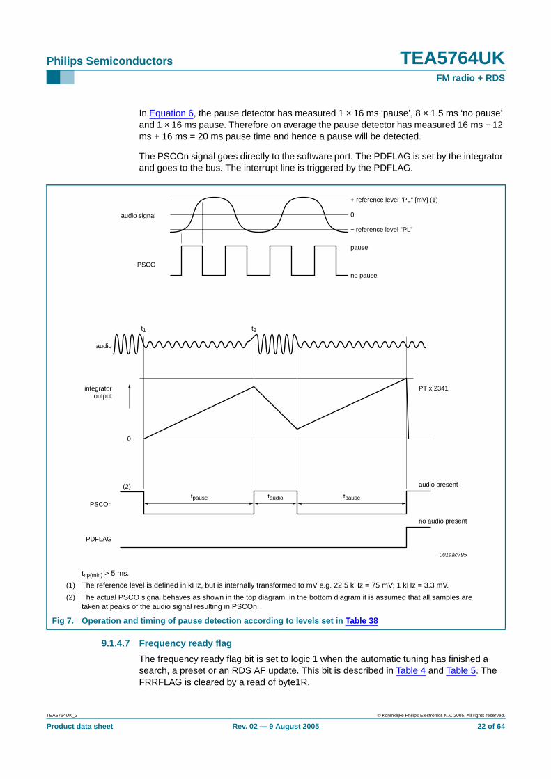
9.1.4.6 Pause detection flag
The pause detector monitors the amplitude of the audio signal and starts counting if itdrops below the reference level. When the counter reaches the specified count time, apause is detected and the PDFLAG is set and will generate an interrupt if bit PDMSK isset to logic 1. The PDFLAG operates independently of bit PDMSK and is only active whenthe RDS decoder is switched on when bit PUPD is set to logic 1 and when the RDSdecoder is not idle if synchronization is lost.
See Figure 7. When the peak audio level of the (L+R) drops below the threshold level at t1it counts the duration of the pause. If the pause lasts longer than the value set by the PTbits, bit PDFLAG is set which in turn generates a hardware interrupt (bit PDMSK set tologic 1). The threshold level at t1 is set by the PL bits shown in Table 38.
Bit PDFLAG is cleared by a read of byte1R on condition that the read action occurs morethan 500 µs after receiving the pause interrupt on the INTX line.
The circuit should ignore short transients where the audio level momentarily rises abovethe threshold (at t2).
A pause is detected by comparing the amplitude of the audio signal with the referencelevel selected by the PL bits. The resultant signal PSCO produced by this comparison issampled at a frequency of 2341 Hz resulting in signal PSCOn. A pause is detected underthe conditions given by Equation 4 and Equation 5.
(4)
(5)
where N is the number of samples taken over time and PT is the pause time selected bybus bits PT. When a pause is detected, the integrator will be reset. The integrator valuecannot be less than zero; therefore if in Equation 4, the value of the second SUMbecomes larger than the first SUM, the output of the integrator remains at zero.
Suppose that PT = 20 ms, tpause = 16 ms and taudio = 1.5 ms. The pause detector willcount according to Equation 5 as shown in Equation 6:
(6)
SUM 0toN 1–( ) PSCOn 0=[ ] 8 SUM 0toN 1–( )× PSCOn 1=[ ]– PT 2341×>
t pause 8 taudio PT>×–
2 tpause 8 t×– audio× 20 ms 2 16 ms 8 1.5 ms×–×≥ 20 ms= =
Product data sheet Rev. 02 — 9 August 2005 21 of 64
Philips Semiconductors TEA5764UKFM radio + RDS
In Equation 6, the pause detector has measured 1 × 16 ms ‘pause’, 8 × 1.5 ms ‘no pause’and 1 × 16 ms pause. Therefore on average the pause detector has measured 16 ms − 12ms + 16 ms = 20 ms pause time and hence a pause will be detected.
The PSCOn signal goes directly to the software port. The PDFLAG is set by the integratorand goes to the bus. The interrupt line is triggered by the PDFLAG.
9.1.4.7 Frequency ready flag
The frequency ready flag bit is set to logic 1 when the automatic tuning has finished asearch, a preset or an RDS AF update. This bit is described in Table 4 and Table 5. TheFRRFLAG is cleared by a read of byte1R.
tnp(min) > 5 ms.
(1) The reference level is defined in kHz, but is internally transformed to mV e.g. 22.5 kHz = 75 mV; 1 kHz = 3.3 mV.
(2) The actual PSCO signal behaves as shown in the top diagram, in the bottom diagram it is assumed that all samples aretaken at peaks of the audio signal resulting in PSCOn.
Fig 7. Operation and timing of pause detection according to levels set in Table 38
Product data sheet Rev. 02 — 9 August 2005 22 of 64
Philips Semiconductors TEA5764UKFM radio + RDS
9.1.4.8 Band limit flag
The band limit bit BLFLAG is set to logic 1 when the automatic tuning has detected theend of the tuning band or when the PLL cannot lock on a certain frequency. This bit isdescribed in Table 4 and Table 5. This bit is cleared by reading byte1R.
9.2 Interrupt outputThe interrupt line driver is a MOS transistor with a nominal sink current of 680 µA, it ispulled HIGH by an 18 kΩ resistor connected to pin VREFDIG. The interrupt line can beconnected to one other similar device with an interrupt output and an 18 kΩ pull-upresistor providing a wired OR function. This allows any of the drivers to pull the line LOWby sinking the current. When a flag is set and not masked it generates an interrupt; seeFigure 8.
10. RDS data processing
The RDS demodulator and decoder perform the following operations:
• Demodulation of the RDS/RDBS data stream from the MPX signal
• Symbol decoding
• Block and group synchronization
• Error detection and correction
• Store last and previous data block received with associated ID and error status
• Set the DAVFLG when new data is received
• Set the SYNC status bit according to the current synchronization state
• Set the LSYNCFL flag when synchronization is lost
The RDS decoder can be set to different modes, each meant to look for specificinformation.
Read INTMSK clears flag, INTMSK and INTX.
Write INTMSK enables INTX.
When flag is set, the next interrupts are blocked until read / write INTMSK.
(1) Flag is set immediately after the reset, because event is still there.
Product data sheet Rev. 02 — 9 August 2005 23 of 64
Philips Semiconductors TEA5764UKFM radio + RDS
10.1 DAV-A processing modeThe DAV-A processing mode is the standard processing mode used. In this mode, when adata block has been decoded, it is transferred to the I2C-bus registers. It generatesinterrupts on the INTX line after every new block of RDS data that has been processedand also sets the DAVFLG; see Figure 9. The DAVFLG is reset by a read of the I2C-busregisters.
If a data block is decoded and a new one arrives, pin INTX goes LOW again, the DAVFLGwill be set and the last block will be shifted to the previous block and the last decodedblock will be put in the last block. This means that all RDS data is still available in the BLand BP registers.
When the I2C-bus registers are not read the DAVFLG will not be reset. If a data block isdecoded and a new one arrives, pin INTX goes LOW and the last block will be shifted tothe previous block and the last decoded block will be put in the last block. This means thatall RDS data is still available in the BL and BP registers but must be read. This is indicatedby the setting of bit DOVF.
If the I2C-bus registers are still not read, data will be lost, except when this read is donewithin 20 ms after the INTX line has gone LOW and 2 ms before the arrival of a new block.If this read is done at least 2 ms before the arrival of a new block, then BL and BP are readand the data in the decoder buffer is then instantaneously shifted to the BL register. Alldata is now read and bit DOVF will be reset.
Product data sheet Rev. 02 — 9 August 2005 24 of 64
Philips Semiconductors TEA5764UKFM radio + RDS
Figure 9 assumes that block synchronization has been achieved and that no otherinterrupt flags are being set.
10.2 DAV-B processing mode / fast PI search modeThis mode is used, for example, when the receiver has been re-tuned to a new station,and a fast search of the PI code, always contained in the A or C’ block, is required. Thediagram shown in Figure 10, assumes that the RDS decoder is unsynchronized initiallyand is performing a synchronization search.
During synchronization search the decoder does not set the DAVFLG until a valid A or C’block is detected. If a valid B block is detected immediately, then the decoder is nowsynchronized and bit SYNC is set to logic 1. In fact, if any 2 good blocks in a valid orderare detected, the RDS decoder will synchronize and give an interrupt.
Bit DOVF set when 2 new blocks received in BL and BP registers
(1) If there is no read cycle, B1 is placed in the BP register and the new block C1 is now in the BLregister. Bit DOVF is set to indicate two blocks available.
(2) Data is not transferred to BL register at the end of the read period/clear DOVF, D1 is missed.
(3) In order not to lose D1 a read must be performed before D1 enters decoder buffer, thus readfinishes within 21 ms after DOVF set to logic 1.
(4) DOVF is cleared when the BL register is read. To be of use, DOVF has to be read before BLand BP registers.
(5) To prevent DOVF being set again, an extra read of BL must be performed before A2 has beendecoded.
Fig 9. DAV-A timing diagram, DAV-A/B: normal
001aab471
A1
21.9 ms
DAVFLGDAVFLG set
on falling edgeDAVN = 0, clearedon read BL register
Product data sheet Rev. 02 — 9 August 2005 25 of 64
Philips Semiconductors TEA5764UKFM radio + RDS
If for some reason a valid B block was not received then the next valid A or C’ block isdecoded and the DAVFLG set. The BP and BL registers record the A block history.
When the decoder is synchronized, each decoded block will set the DAVFLG (assuming itwas reset by a read action) and generate an interrupt.
10.3 DAV-C reduced processing modeThe DAV-C processing mode is very similar to DAV-A mode with the main exception that adata flag is set only after two new blocks are received. Hence the update rate is reducedby half.
When the number of blocks detected in the order: ‘bad’ ‘bad’ ‘good’ is 2, synchronization isachieved if another good block followed by either 0, 1 or 2 bad blocks and another good blockare then received. If the order is 3 bad blocks, no synchronization is achieved and the countersare reset.
The number of allowed bad clocks can be set using the BBG bits
Fig 10. DAV-A timing diagram, DAV B: with bad blocks detected during sync search
001aab472
B1
21.9 ms
only valid blocks with no errorsare counted as good blocks
Product data sheet Rev. 02 — 9 August 2005 26 of 64
Philips Semiconductors TEA5764UKFM radio + RDS
Fig 11. Normal DAV-C timing diagram
Fig 12. DAV-C timing diagram, late read of BL, BP register
001aab473
A1
21.9 ms
B1
DAVFLG cleared at end read BP registerand forced to zero till end read of RDS 4R
BL register copied toBP register and C1 toBL register
B1 copied to BL register shortlybefore C1 decoded
INTX cleared at end read INTMSKtINTX
tINT_RD
tread
DAVFLG
beingdecoded
read access(case 1)
INTX
C1 D1 A2 B2
001aab474
A1
21.9 ms
B1
DAVFLG reset when1st new blockwould have been copied DAVFLG set when 2nd new block
in decoder buffer
instant copy of A2from decoderbuffer to BL, and BL to BP
instant copy C1 from decoder bufferto BL, and BL to BP just before D1decoded due to read action
(a)
DAVFLG not cleared as no read performed
tread
tINTX = 10 ms
INTX
read access(case 2)
dataoverflow bit
no read on INTXso B1 will be lost
2 new blocks have arrived in BL/BP (C1, D1) and a new block (A2)has entered the decoder buffer. Hence, DOVF is set again.To prevent this, an extra read must be performed after reading (a)
dashed line shows what would happen if no readoccurred at (a). DOVF bit set until the next read of BP
Product data sheet Rev. 02 — 9 August 2005 27 of 64
Philips Semiconductors TEA5764UKFM radio + RDS
10.4 Synchronization
10.4.1 Conditions for synchronization
When the RDS decoder is turned on it must be synchronized to extract valid data from theMPX signal. To do so the decoder automatically initiates a search for synchronization. Theconditions to meet synchronization and the status of this synchronization can be set andchecked by the following bits:
• BBL (Bad Blocks Lose): these bits can be set via the I2C-bus and have a valuebetween 0 to 63
• GBL (Good Blocks Lose): these bits can be set via the I2C-bus and have a valuebetween 0 to 63
• BBG (Bad Blocks Gain): these bits can be set via the I2C-bus and have a valuebetween 0 to 32
• GBC (Good Block Count): these bits can be read via the I2C-bus and have a valuebetween 0 to 63
• BBC (Bad Block Count): these bits can be read via the I2C-bus and have a valuebetween 0 to 63
When the decoder is not synchronized it will initiate a synchronization search. Thisinvolves calculation of the syndrome for each block of 26 received bits on a bit-by-bitbasis. When a correct syndrome (and hence block ID) is received the decoder clocks thenext 26 bits into the internal registers and performs a second syndrome check.Synchronization is found when a certain number of blocks have been decoded and twogood blocks have been found, this number of blocks is defined by the BBG bits. If the firstblock needed for synchronization has been found and the expected second block (after26 bits) is an invalid block, then the decoder module internal bad_blocks_counter isincremented and the next expected block is calculated; exception: if RBDS mode isselected and the first block is E, then the next expected block is always block A, untilsynchronization is found or the maximum bad_blocks_counter value is reached. If thedecoder module internal bad_blocks_counter reaches the value of BBG[4:0], then a newsynchronization search (bit-by-bit) is started immediately to find a new first block.
The synchronization is monitored by two flywheel counters, GBC and BBC. These are6-bit counters that can be preset by bits GBL and BBL to values between 0 and 63. Eachtime a block is decoded and recognized as a bad block the Bad Block Counter value,BBC, is incremented by 1. When the BBC value is equal to the BBL value, synchronizationis lost. Bit SYNC will become 0 and bit LSYNCFL is set to indicate the loss ofsynchronization. The TEA5764UK will now automatically initiate a new synchronizationsearch.
Each time a good block is decoded, the GBC value is incremented. When the GBC valueis equal to the GBL value, both counters, BBC and GBC, are set to 0 and a new countstarts. The GBC counter is only incremented when the decoder is synchronized.
Product data sheet Rev. 02 — 9 August 2005 28 of 64
Philips Semiconductors TEA5764UKFM radio + RDS
10.4.2 Data overflow
During synchronization, after RDS data is read from the registers, new available blocksare shifted to the registers as described in Section 10.1 to Section 10.3. If the registersare not read in time, the decoder cannot shift any new available block to the registers andhence a data overflow will occur, this is indicated by bit DOVF which is set to 1. Bit DOVFis reset by a read of the registers or if bit NWSY = 1 which results in the start of a newsynchronization search.
Each time when a RDS data block is decoded, bit DAVN goes to logic 0 to indicate thepresence of a new data block. Bit DAVN also triggers the interrupt output INTX. Inprinciple the microprocessor must now start reading and must have read all RDS data(byte12R to byte19R) before the arrival of a new RDS data block. In the application it ispossible that there is too large a delay between the arrival of a new block and reading thisblock. This can have various causes such as a microprocessor that has to start-up fromSleep mode or when polling is used instead of interrupt based read actions. Figure 13shows the behavior of bit DAVFLG and bit DAVN when polling, where reading can occur atany time. Note: Bit DAVN sets the INTX oneshot generator when DAVMSK = 1. UnlikeINTX, bit DAVN is not cleared by a read of the mask register.
Product data sheet Rev. 02 — 9 August 2005 29 of 64
xxxxxxxxxxxxxxxxxxxxx xxxxxxxxxxxxxxxxxxxxxxxxxx xxxxxxx x x x xxxxxxxxxxxxxxxxxxxxxxxxxxxxxx xxxxxxxxxxxxxxxxxxx xx xxxxxxx xxxxxxxxxxxxxxxxxxxxxxxxxxx xxxxxxxxxxxxxxxxxxx xxxxxx xxxxxxxxxxxxxxxxxxxxxxxxxxxxxxxxxxx xxxxxxxxxxxx x xxxxxxxxxxxxxxxxxxxxxx xxxxxxxxxxxxxxxxxxxxxxxxxxxxxx xxxxx xxxxxxxxxxxxxxxxxxxxxxxxxxxxxxxxxxxxxxxxxxxxxxxxxx xxxxxxxxxxxxxxxxxxxxxxxxxxxxxxxxx xxxxxxxxxxxxxxxxxxxx xxx
Blocking DAVFLG: at end of reading byte15R or byte17R (DAV-A, B/C) DAVFLG is forced to zero. Only after reading byte19R
If synchronous reading is performed using ASIC generated interrupts, this problem does not occur.
To prevent undefined situations, byte12R to byte19R should always be read in one action immediately after each other.
Signal DAVN ≠ INTX.
(1) Normally reading byte19R would reset bit DAVN, but now it is reset after 10 ms, the maximal LOW time of bit DAVN.
(2) Read of byte15R in DAV-A and DAV-B mode clears DAVFLG. In DAV-C mode two consecutive RDS data blocks are read andbyte17R instead of byte15R (dotted line).
(3) Read of byte19R clears bit DAVN.
(4) Write byte0W (interrupt register).
Fig 13. RDS flag behavior
BARDS data
DAVN
DAVFLG
reset of DAVFLG
Read byte: 15R0R 19R 0W
17R
C D A
(2) (3) (4)
10
15R0R 19R 0W
17R
15R0R 19R 0W
17R
15R0R 19R 0W
17R
15R0R 19R 0W
17R
Philips Semiconductors TEA5764UKFM radio + RDS
10.6 Error detection and reportingThe TDA5764UK must report information on the number of errors corrected in the last andpreviously decoded blocks. This is reported in bits ELB and EPB as shown in Table 29.
During synchronization search the error correction is disabled for detection of the firstblock and is enabled for processing of the second block according to the mode set by theSYM bits as described in Table 36.
10.7 RDS test modesIn Test mode the raw RDS clock and RDS data can be recovered directly from pins VAFLand VAFR when bit RDSCDA = 1.
10.8 Reading RDS data from the registersTo read RDS data the microprocessor must read byte12R to byte19R. All 8 bytes must beread to reset the status bytes 12R and 13R, i.e. effectively the status bits can be updatedby the decoder after reading the last bit of byte19R. Bit DOVF is cleared after reading thelast bit of byte19R and the status of bit SYNC does not depend on reading the register, bitSYNC indicates if the decoder is synchronized or not. When starting a read action frombyte12R, the decoder blocks updates from the RDS bytes until byte19R has been read.RDS byte12R to byte19R must be read in one read action.
11. I2C-bus interface
The I2C-bus interface is based on “The I2C-bus specification”, version 2.1 January 2000,expanded by the following definitions.
11.1 Write and read mode
When writing all bytes, byte0W to byte10W can be written with one write action.
Product data sheet Rev. 02 — 9 August 2005 31 of 64
Philips Semiconductors TEA5764UKFM radio + RDS
When the TEA5764UK is addressed by the FM radio address, the RDS part (byte12R tobyte27R) can be read in one read action. A read does not have to stop at byte11R.
Therefore, by effectively only using the RDS part of the address, ignores some byteswhich reduces I2C-bus access.
11.2 Data transferStructure of the I2C-bus:
• Slave transceiver
• Subaddresses not used
• Maximum LOW-level input voltage: VIL = 0.3 × VVREFDIG
Remark: The I2C-bus operates at a maximum clock rate of 400 kHz. It is not allowed toconnect the TEA5764UK to a I2C-bus operating at a higher clock rate.
Data transfer to the IC:
• Bit 7 of each byte is considered the MSB and has to be transferred as the first bit ofthe byte
• The LSB indicates the write or read action
• The data becomes valid byte-wise at the appropriate falling edge of the SCL clock
• A STOP condition after any byte can shorten transmission times. When writing to thetransceiver by using the STOP condition before completion of the whole transfer:
– The remaining bytes will contain the old information
– If the transfer of a byte is not completed the new bits will be used, but a new tuningcycle will not be started
Product data sheet Rev. 02 — 9 August 2005 32 of 64
Philips Semiconductors TEA5764UKFM radio + RDS
To speed up RDS traffic it is possible to read all the RDS data and then only write backbyte INTMSK to set the appropriate mask(s) again.
I2C-bus activity:
• With bits PUPD the TEA5764UK can be switched in a low current Standby mode. TheI2C-bus is then still active
• When the I2C-bus interface is deactivated, by making pin BUSENABLE LOW andwithout programmed Standby mode, the TEA5764UK keeps its normal operation, butis isolated from the I2C-bus lines
• It is possible to operate the TEA5764UK with BUSENABLE hard wired to pinVREFDIG, and have the bus interface always active.
tf = fall time of both SDA and SCL signals: 20 + 0.1 Cb < tf < 300 ns, where Cb = total capacitance on bus line in pF.
tr = rise time of both SDA and SCL signals: 20 + 0.1 Cb < tf < 300 ns, where Cb = total capacitance on bus line in pF.
tHD;STA = hold time (repeated) START condition. After this period, the first clock pulse is generated: > 600 ns.
tHIGH = HIGH period of the SCL clock: > 600 ns.
tSU;STA = setup time for a repeated START condition: > 600 ns.
tHD;DAT = data hold time: 300 < tHD;DAT < 900 ns.
Remark: 300 ns lower limit is added because the ASIC has no internal hold time for the SDA signal.
tSU;DAT = data setup time: tSU;DAT > 100 ns. If ASIC is used in a standard mode I2C-bus system, tSU;DAT > 250 ns.
tSU;STO = setup time for STOP condition: > 600 ns.
tBUF = bus free time between a STOP and a START condition: > 600 ns.
Cb = capacitive load of one bus line: < 400 pF.
tSU;BUSEN = bus enable setup time: tSU;BUSEN > 10 µs.
tHO;BUSEN = bus enable hold time: tHO:BUSEN > 10 µs.
Product data sheet Rev. 02 — 9 August 2005 37 of 64
Philips Semiconductors TEA5764UKFM radio + RDS
[1] This bit does not switch the radio to mono or stereo, this depends on the RF input level as shown in sections‘Mono stereo blend’ or ‘mono stereo switched’ in Table 46.
Table 23: LEVCHK - byte9R description
Bit Symbol Access Reset Functional description
7 LEV3 R - level count MSB
6 LEV2 R - level count bit
5 LEV1 R - level count bit
4 LEV0 R - level count LSB
3 LD R - 1 = PLL is locked
0 = PLL is not locked
2 STEREO R - 1 = pilot detected [1]
0 = no pilot detected
1 and 0 - - - reserved
Table 24: TESTBITS - byte10R and byte5W description
Bit Symbol Access Reset Functional description
7 LHM R/W 0 1 = left audio output is hard muted
0 = left audio output is not hard muted
6 RHM R/W 0 1 = right audio output is hard muted
0 = right audio output is not hard muted
5 RDSCDA R/W 0 1 = pin VAFL is RDS clock and pin VAFR isRDS data
0 = normal operation
4 LHSW R/W 0 1 = level hysteresis is large
0 = level hysteresis is small
3 TRIGFR R/W 0 1 = reference frequency selected pinFREQIN
0 = crystal as reference pin XTAL
2 LDX R/W 0 1 = local DX on, −6 dB gain of LNA
0 = local DX off, LNA has normal gain
1 RFAGC R/W 0 1 = RFAGC off
0 = RFAGC on
0 INTCTRL R/W 0 when this bit is set to logic 1 an interrupt isgenerated on pin INTX
Product data sheet Rev. 02 — 9 August 2005 38 of 64
Philips Semiconductors TEA5764UKFM radio + RDS
Table 25: TESTMODE - byte11R and byte6W description
Bit Symbol Access Reset Functional description
7 to 5 - R/W 0 reserved
4 TM R/W 0 1 = oscillator output and programmabledivider output are enabled
0 = normal operation
3 TB3 R/W 0 test bits: Table 27 describes selection ofsignals output to the SWPORT whenSWPM = 0; when TM = 1; TB[3:0] = 0;which effectively is an AND function.
Product data sheet Rev. 02 — 9 August 2005 45 of 64
Philips Semiconductors TEA5764UKFM radio + RDS
13. Static characteristics
Table 45: CharacteristicsThe minimum and maximum values include spread due to VCCA = VCCD = 2.5 V to 3.3 V and Tamb = −20 °C to +85 °C; unlessotherwise specified.
Symbol Parameter Conditions Min Typ Max Unit
Supply voltages
VCCA analog supply voltage 2.5 2.7 3.3 V
VCCD digital supply voltage 2.5 2.7 3.3 V
VVREFDIG digital reference voltage forI2C-bus interface on pinVREFDIG
1.65 1.8 VCCD V
Supply currents
ICCA analog supply current VCCA = 2.5 V to 3.3 V
operating mode 12 13.7 16 mA
Standby mode 0 0.1 1 µA
ICCD digital supply current VCCD = 2.5 V to 3.3 V
operating mode 0.3 0.7 1.5 mA
Standby mode 1 15 22.5 µA
IVREFDIG digital reference supply current operating mode;VVREFDIG = 1.65 V to VCCD
0 0.5 1 µA
DC operating points
VLOOPSW voltage on pin LOOPSW VCD3 − 0.2 - VCD3 V
VCPOUT voltage on pin CPOUT 0.1 - VCD3 − 0.1 V
VLO1 voltage on pin LO1 VCD3 − 0.1 - VCD3 V
VLO2 voltage on pin LO2 VCD3 − 0.1 - VCD3 V
VPILLP voltage on pin PILLP 1.09 1.37 1.65 V
VTMUTE voltage on pin TMUTE VRF = 0 V, measured withrespect to pin CD3
0.6 0.7 0.8 mV
VVAFL voltage on pin VAFL fRF = 98 MHz; VRF = 1 mV;no modulation
800 850 940 mV
VVAFR voltage on pin VAFR fRF = 98 MHz; VRF = 1 mV;no modulation
800 850 940 mV
VMPXOUT voltage on pin MPXOUT fRF = 98 MHz; VRF = 1 mV;no modulation
830 900 950 mV
VMPXIN voltage on pin MPXIN fRF = 98 MHz; VRF = 1 mV;no modulation
0.2 0.4 0.5 V
VFREQIN voltage on pin FREQIN TRIGFR = 1 1.3 1.5 1.7 V
TRIGFR = 0 0 0.05 0.1 V
VXTAL voltage on pin XTAL to CD3 TRIGFR = 1 0.9 1.17 1.3 V
Product data sheet Rev. 02 — 9 August 2005 46 of 64
Philips Semiconductors TEA5764UKFM radio + RDS
14. Dynamic characteristics
Table 46: CharacteristicsSee Figure 1; all AC values are given in RMS; the minimum and maximum values include spread due to VCCA = VCCD = 2.5 Vto 3.3 V and Tamb = −20 °C to +85 °C; unless otherwise specified. All RF input values are defined in potential difference,except when EMF is explicitly stated.
Symbol Parameter Conditions Min Typ Max Unit
Voltage controlled oscillator
fosc oscillator frequency 150 - 217 MHz
Reference frequency input; pin FREQIN
Ri input resistance 500 - - kΩ
Ci input capacitance 5 6 7 pF
frsn resonance frequency - 32.768 - kHz
∆frsn resonance frequency deviation Tamb = 25 °C −20 - +20 ppm
Tamb = −20 °C to +85 °C −150 - +150 ppm
δ duty cycle square wave 30 - 70 %
VIH HIGH-level input voltage square wave 1.15 - VCC V
VIL LOW-level input voltage square wave 0 - 0.55 V
C/N carrier-to-noise ratio at 10 kHz −151 - - dBc/Hz
Crystal oscillator 32.768 kHz; pin XTAL
frsn resonance frequency Tamb = 25 °C - 32.768 - kHz
∆frsn resonance frequency deviation −20 - +20 ppm
Cshunt shunt capacitance - - 3.5 pF
Cm motional capacitance 1.5 - 3.0 fF
Rs series resistance - - 75 kΩ
Synthesizer
Programmable divider
D/Dprog programmable divider ratio FRQSETMSB[15:8] = XX111111; FRQSETLSB[7:0] =1111 1110
Product data sheet Rev. 02 — 9 August 2005 47 of 64
Philips Semiconductors TEA5764UKFM radio + RDS
Logic pins; pins BUSENABLE, SCL and SDA
Ri input resistance 10 - - MΩ
VIH HIGH-level input voltage input switching level up 0.7VVREFDIG - VVREFDIG +0.3
V
VIL LOW-level input voltage input switching level down −0.3 - 0.3VVREFDIG V
Software programmable port; pin SWPORT
VO(max) maximum output voltage Iload = 150 µA VVREFDIG −0.2
- VVREFDIG V
VO(min) minimum output voltage Iload = 150 µA 0 - 0.2 V
Isink(max) maximum sink current 400 - 2000 µA
Isource(max) maximum source current 500 - 1100 µA
IL(max) maximum leakage current VSWPORT = 0 V to 5 V −1.0 - +1.0 µA
Interrupt flag; pin INTX; V VREFDIG = 1.65 V to 1.95 V; I load(max) = 200 µA or R pu of second device connected to pinINTX is 18 k Ω ± 20 %
VO(max) maximum output voltage VVREFDIG −0.2
- VVREFDIG V
VO(min) minimum output voltage 0.130 0.215 0.4 V
Ipd pull-down current 500 680 1200 µA
Rpu pull-up resistance 14.4 18 22.5 kΩ
tL LOW time one-shot pulse time 9.9 9.98 10 ms
Table 46: Characteristics …continuedSee Figure 1; all AC values are given in RMS; the minimum and maximum values include spread due to VCCA = VCCD = 2.5 Vto 3.3 V and Tamb = −20 °C to +85 °C; unless otherwise specified. All RF input values are defined in potential difference,except when EMF is explicitly stated.
Symbol Parameter Conditions Min Typ Max Unit
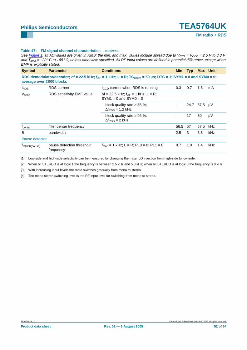
Table 47: FM signal channel characteristicsSee Figure 1; all AC values are given in RMS; the min. and max. values include spread due to VCCA = VCCD = 2.5 V to 3.3 Vand Tamb = −20 °C to +85 °C; unless otherwise specified. All RF input values are defined in potential difference, except whenEMF is explicitly stated.
Symbol Parameter Conditions Min Typ Max Unit
FM RF input; pins RFIN1 and RFIN2
Ri input resistance connected to pin GNDRF 75 100 125 Ω
Ci input capacitance connected to pin GNDRF 2.5 4 6 pF
Vsens(EMF) sensitivity EMF value voltage fRF = 76 MHz to 108 MHz;∆f = 22.5 kHz; fmod = 1 kHz;(S+N)/N = 26 dB; TCdeem= 75 µs;A-weighting filter;Baud = 300 Hz to 15 kHz
- 2.9 4.4 µV
IP3in in-band 3rd-order interceptpoint
∆f1 = 200 kHz; ∆f2 = 400 kHz;ftune = 76 MHz to 108 MHz; RFagc = off
78 87 - dBµV
IP3out out-of-band 3rd-orderintercept point
∆f1 = 4 MHz; ∆f2 = 8 MHz;ftune = 76 MHz to 108 MHz; RFagc = off
AMsup AM suppression L = R; ∆f = 22.5 kHz; fmod = 1 kHz;VRF = 100 µV to 10 mV; m = 0.3;DTC = 0; Baud = 300 Hz to 15 kHz
−40 - - dB
Table 47: FM signal channel characteristics …continuedSee Figure 1; all AC values are given in RMS; the min. and max. values include spread due to VCCA = VCCD = 2.5 V to 3.3 Vand Tamb = −20 °C to +85 °C; unless otherwise specified. All RF input values are defined in potential difference, except whenEMF is explicitly stated.
Table 47: FM signal channel characteristics …continuedSee Figure 1; all AC values are given in RMS; the min. and max. values include spread due to VCCA = VCCD = 2.5 V to 3.3 Vand Tamb = −20 °C to +85 °C; unless otherwise specified. All RF input values are defined in potential difference, except whenEMF is explicitly stated.
Product data sheet Rev. 02 — 9 August 2005 50 of 64
Philips Semiconductors TEA5764UKFM radio + RDS
THD total harmonic distortion VRF = 1 mV; L = 1; R = 0; ∆f = 75 kHzincluding 9 % pilot deviation;fmod = 1 kHz; DTC = 0; Baud = 300 Hzto 15 kHz; A-weighting filter
mono; L = R; no pilot deviation - 0.4 0.9 %
stereo; L = 1, R = 0; 9 % pilotdeviation; see Figure 17
- 0.9 2.5 %
αsup(pilot) pilot suppression measured at pins VAFL and VAFR;related to ∆f = 75 kHz including 9 %pilot deviation; fmod = 1 kHz; DTC = 0
40 50 - dB
∆fpilot pilot frequency deviation VRF = 1 mV Table note [2]
αhys(pilot) pilot tone detection hysteresis VRF = 1 mV 2 - 6 dB
TCdeem de-emphasis time constant VRF = 1 mV
DTC = 1 38 50 62 µs
DTC = 0 57 75 93 µs
Mono stereo blend; SNC = 1
Vstart(blend) blend start voltage αcs = 0.5 dB [3] 2 7 15 µV
αcs channel separation VRF = 30 µV; ∆f = 75 kHz including 9 %pilot deviation; R = 1 and L = 0 or R = 0and L = 1; fmod = 1 kHz; MST = 0;SNC = 1
4 10 16 dB
Mono stereo switching; ∆f = 75 kHz including 9 % pilot deviation; f mod = 1 kHz; SNC = 0
αcs channel separation MST = 0; R = 1 and L = 0 or R = 0 andL = 1
VRF = 30 µV; increasing RF inputlevel
27 33 - dB
VRF = 10 µV; decreasing RF inputlevel
- - 1 dB
Vsw switching voltage [4] 17 25 45 µV
hys hysteresis [4] 3 3.5 4 dB
Bus driven mute functions
Tuning mute; AFM = 1
αmute(VAFR) mute depth on pin VAFR AFM = 1 or RHM = 1; ∆f = 75 kHz;mono; Baud = 300 Hz to 15 kHz;A-weighting filter
−60 - - dB
αmute(VAFL) mute depth on pin VAFL AFM = 1 or LHM = 1; ∆f = 75 kHz;mono; Baud = 300 Hz to 15 kHz;A-weighting filter
−60 - - dB
αmute mute depth on pins VAFL andVAFR
MU = 1; ∆f = 75 kHz; mono;Baud = 300 Hz to 15 kHz; A-weightingfilter
−80 - - dB
Table 47: FM signal channel characteristics …continuedSee Figure 1; all AC values are given in RMS; the min. and max. values include spread due to VCCA = VCCD = 2.5 V to 3.3 Vand Tamb = −20 °C to +85 °C; unless otherwise specified. All RF input values are defined in potential difference, except whenEMF is explicitly stated.
Table 47: FM signal channel characteristics …continuedSee Figure 1; all AC values are given in RMS; the min. and max. values include spread due to VCCA = VCCD = 2.5 V to 3.3 Vand Tamb = −20 °C to +85 °C; unless otherwise specified. All RF input values are defined in potential difference, except whenEMF is explicitly stated.
Product data sheet Rev. 02 — 9 August 2005 57 of 64
Philips Semiconductors TEA5764UKFM radio + RDS
17. Soldering
17.1 Introduction to soldering surface mount packagesThis text gives a very brief insight to a complex technology. A more in-depth account ofsoldering ICs can be found in our Data Handbook IC26; Integrated Circuit Packages(document order number 9398 652 90011).
There is no soldering method that is ideal for all surface mount IC packages. Wavesoldering can still be used for certain surface mount ICs, but it is not suitable for fine pitchSMDs. In these situations reflow soldering is recommended.
17.2 Reflow solderingReflow soldering requires solder paste (a suspension of fine solder particles, flux andbinding agent) to be applied to the printed-circuit board by screen printing, stencilling orpressure-syringe dispensing before package placement. Driven by legislation andenvironmental forces the worldwide use of lead-free solder pastes is increasing.
Several methods exist for reflowing; for example, convection or convection/infraredheating in a conveyor type oven. Throughput times (preheating, soldering and cooling)vary between 100 seconds and 200 seconds depending on heating method.
Typical reflow peak temperatures range from 215 °C to 270 °C depending on solder pastematerial. The top-surface temperature of the packages should preferably be kept:
• below 225 °C (SnPb process) or below 245 °C (Pb-free process)
– for all BGA, HTSSON..T and SSOP..T packages
– for packages with a thickness ≥ 2.5 mm
– for packages with a thickness < 2.5 mm and a volume ≥ 350 mm3 so calledthick/large packages.
• below 240 °C (SnPb process) or below 260 °C (Pb-free process) for packages with athickness < 2.5 mm and a volume < 350 mm3 so called small/thin packages.
Moisture sensitivity precautions, as indicated on packing, must be respected at all times.
17.3 Wave solderingConventional single wave soldering is not recommended for surface mount devices(SMDs) or printed-circuit boards with a high component density, as solder bridging andnon-wetting can present major problems.
To overcome these problems the double-wave soldering method was specificallydeveloped.
If wave soldering is used the following conditions must be observed for optimal results:
• Use a double-wave soldering method comprising a turbulent wave with high upwardpressure followed by a smooth laminar wave.
• For packages with leads on two sides and a pitch (e):
– larger than or equal to 1.27 mm, the footprint longitudinal axis is preferred to beparallel to the transport direction of the printed-circuit board;
Product data sheet Rev. 02 — 9 August 2005 58 of 64
Philips Semiconductors TEA5764UKFM radio + RDS
– smaller than 1.27 mm, the footprint longitudinal axis must be parallel to thetransport direction of the printed-circuit board.
The footprint must incorporate solder thieves at the downstream end.
• For packages with leads on four sides, the footprint must be placed at a 45° angle tothe transport direction of the printed-circuit board. The footprint must incorporatesolder thieves downstream and at the side corners.
During placement and before soldering, the package must be fixed with a droplet ofadhesive. The adhesive can be applied by screen printing, pin transfer or syringedispensing. The package can be soldered after the adhesive is cured.
Typical dwell time of the leads in the wave ranges from 3 seconds to 4 seconds at 250 °Cor 265 °C, depending on solder material applied, SnPb or Pb-free respectively.
A mildly-activated flux will eliminate the need for removal of corrosive residues in mostapplications.
17.4 Manual solderingFix the component by first soldering two diagonally-opposite end leads. Use a low voltage(24 V or less) soldering iron applied to the flat part of the lead. Contact time must belimited to 10 seconds at up to 300 °C.
When using a dedicated tool, all other leads can be soldered in one operation within2 seconds to 5 seconds between 270 °C and 320 °C.
17.5 Package related soldering information
[1] For more detailed information on the BGA packages refer to the (LF)BGA Application Note (AN01026);order a copy from your Philips Semiconductors sales office.
[2] All surface mount (SMD) packages are moisture sensitive. Depending upon the moisture content, themaximum temperature (with respect to time) and body size of the package, there is a risk that internal orexternal package cracks may occur due to vaporization of the moisture in them (the so called popcorneffect). For details, refer to the Drypack information in the Data Handbook IC26; Integrated CircuitPackages; Section: Packing Methods.
[3] These transparent plastic packages are extremely sensitive to reflow soldering conditions and must on noaccount be processed through more than one soldering cycle or subjected to infrared reflow soldering withpeak temperature exceeding 217 °C ± 10 °C measured in the atmosphere of the reflow oven. The packagebody peak temperature must be kept as low as possible.
Table 49: Suitability of surface mount IC packages for wave and reflow soldering methods
Product data sheet Rev. 02 — 9 August 2005 59 of 64
Philips Semiconductors TEA5764UKFM radio + RDS
[4] These packages are not suitable for wave soldering. On versions with the heatsink on the bottom side, thesolder cannot penetrate between the printed-circuit board and the heatsink. On versions with the heatsinkon the top side, the solder might be deposited on the heatsink surface.
[5] If wave soldering is considered, then the package must be placed at a 45° angle to the solder wavedirection. The package footprint must incorporate solder thieves downstream and at the side corners.
[6] Wave soldering is suitable for LQFP, QFP and TQFP packages with a pitch (e) larger than 0.8 mm; it isdefinitely not suitable for packages with a pitch (e) equal to or smaller than 0.65 mm.
[7] Wave soldering is suitable for SSOP, TSSOP, VSO and VSSOP packages with a pitch (e) equal to or largerthan 0.65 mm; it is definitely not suitable for packages with a pitch (e) equal to or smaller than 0.5 mm.
[8] Image sensor packages in principle should not be soldered. They are mounted in sockets or deliveredpre-mounted on flex foil. However, the image sensor package can be mounted by the client on a flex foil byusing a hot bar soldering process. The appropriate soldering profile can be provided on request.
[9] Hot bar soldering or manual soldering is suitable for PMFP packages.
Product data sheet Rev. 02 — 9 August 2005 61 of 64
Philips Semiconductors TEA5764UKFM radio + RDS
19. Data sheet status
[1] Please consult the most recently issued data sheet before initiating or completing a design.
[2] The product status of the device(s) described in this data sheet may have changed since this data sheet was published. The latest information is available on the Internet atURL http://www.semiconductors.philips.com.
[3] For data sheets describing multiple type numbers, the highest-level product status determines the data sheet status.
20. Definitions
Short-form specification — The data in a short-form specification isextracted from a full data sheet with the same type number and title. Fordetailed information see the relevant data sheet or data handbook.
Limiting values definition — Limiting values given are in accordance withthe Absolute Maximum Rating System (IEC 60134). Stress above one ormore of the limiting values may cause permanent damage to the device.These are stress ratings only and operation of the device at these or at anyother conditions above those given in the Characteristics sections of thespecification is not implied. Exposure to limiting values for extended periodsmay affect device reliability.
Application information — Applications that are described herein for anyof these products are for illustrative purposes only. Philips Semiconductorsmake no representation or warranty that such applications will be suitable forthe specified use without further testing or modification.
21. Disclaimers
Life support — These products are not designed for use in life supportappliances, devices, or systems where malfunction of these products canreasonably be expected to result in personal injury. Philips Semiconductors
customers using or selling these products for use in such applications do soat their own risk and agree to fully indemnify Philips Semiconductors for anydamages resulting from such application.
Right to make changes — Philips Semiconductors reserves the right tomake changes in the products - including circuits, standard cells, and/orsoftware - described or contained herein in order to improve design and/orperformance. When the product is in full production (status ‘Production’),relevant changes will be communicated via a Customer Product/ProcessChange Notification (CPCN). Philips Semiconductors assumes noresponsibility or liability for the use of any of these products, conveys nolicense or title under any patent, copyright, or mask work right to theseproducts, and makes no representations or warranties that these products arefree from patent, copyright, or mask work right infringement, unless otherwisespecified.
22. Trademarks
Notice — All referenced brands, product names, service names andtrademarks are the property of their respective owners.I2C-bus — wordmark and logo are trademarks of Koninklijke PhilipsElectronics N.V.
23. Contact information
For additional information, please visit: http://www.semiconductors.philips.com
Level Data sheet status [1] Product status [2] [3] Definition
I Objective data Development This data sheet contains data from the objective specification for product development. PhilipsSemiconductors reserves the right to change the specification in any manner without notice.
II Preliminary data Qualification This data sheet contains data from the preliminary specification. Supplementary data will be publishedat a later date. Philips Semiconductors reserves the right to change the specification without notice, inorder to improve the design and supply the best possible product.
III Product data Production This data sheet contains data from the product specification. Philips Semiconductors reserves theright to make changes at any time in order to improve the design, manufacturing and supply. Relevantchanges will be communicated via a Customer Product/Process Change Notification (CPCN).