This document contains information on a new product under development by Motorola.Motorola reserves the right to change or discontinue this product without notice.
The Motorola MPC106 PCI bridge/memory controller provides a PowerPC™ microprocessor commonhardware reference platform (CHRP™) compliant bridge between the PowerPC microprocessor familyand the Peripheral Component Interconnect (PCI) bus. In this document, the term ‘106’ is used as anabbreviation for the phrase ‘MPC106 PCI bridge/memory controller.’ This document contains pertinentphysical characteristics of the 106. For functional characteristics, refer to the
MPC106 PCIBridge/Memory Controller User’s Manual
.
This document contains the following topics:
Topic Page
Section 1.1, “Overview” 2
Section 1.2, “Features” 3
Section 1.3, “General Parameters” 5
Section 1.4, “Electrical and Thermal Characteristics” 5
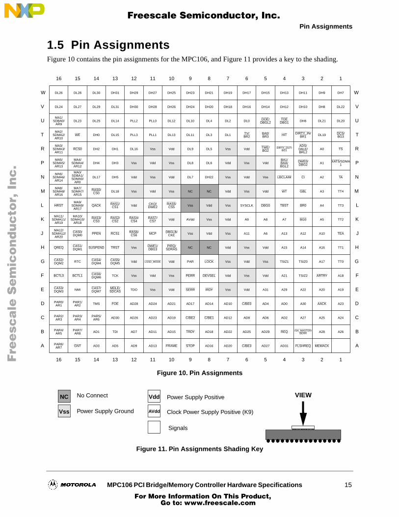
Section 1.5, “Pin Assignments” 15
Section 1.6, “Pinout Listings 16
Section 1.7, “Package Description” 20
Section 1.8, “System Design Information” 22
Section 1.9, “Document Revision History” 27
Section 1.10, “Ordering Information” 27
Fre
esc
ale
Se
mic
on
du
cto
r, I
Freescale Semiconductor, Inc.
For More Information On This Product, Go to: www.freescale.com
In this document, the term ‘60x’ is used to denote a 32-bit microprocessor from the PowerPC architecturefamily that conforms to the bus interface of the PowerPC 601™, PowerPC 603™, or PowerPC 604™microprocessors. Note that this does not include the PowerPC 602™ microprocessor which has amultiplexed address/data bus. 60x processors implement the PowerPC architecture as it is specified for32-bit addressing, which provides 32-bit effective (logical) addresses, integer data types of 8, 16, and 32bits, and floating-point data types of 32 and 64 bits (single-precision and double-precision).
To locate any published errata or updates for this document, refer to the website athttp://www.mot.com/SPS/PowerPC/.
1.1 Overview
The MPC106 provides an integrated high-bandwidth, high-performance, TTL-compatible interfacebetween a 60x processor, a secondary (L2) cache or additional (up to four total) 60x processors, the PCIbus, and main memory. This section provides a block diagram showing the major functional units of the106 and describes briefly how those units interact.
Figure 1 shows the major functional units within the 106. Note that this is a conceptual block diagramintended to show the basic features rather than how these features are physically implemented on thedevice.
Figure 1. Block Diagram
Target Master
PCI Interface
PCI Bus
MemoryInterface
Power Management
Error/InterruptControl
ConfigurationRegisters
L2
60x ProcessorInterface
L2 CacheInterface
60x BusMemory
Fre
esc
ale
Se
mic
on
du
cto
r, I
Freescale Semiconductor, Inc.
For More Information On This Product, Go to: www.freescale.com
The 106 provides a PowerPC microprocessor CHRP-compliant bridge between the PowerPCmicroprocessor family and the PCI bus. CHRP documentation provides a set of specifications that define aunified personal computer architecture. PCI support allows the rapid design of systems using peripheralsalready designed for PCI and the other standard interfaces available in the personal computer hardwareenvironment. The 106 integrates secondary cache control and a high-performance memory controller, usesan advanced, 3.3-V CMOS process technology, and is fully compatible with TTL devices.
The 106 supports a programmable interface to a variety of PowerPC microprocessors operating at selectbus speeds. The 60x address bus is 32 bits wide and the data bus is 64 bits wide. The 60x processorinterface of the 106 uses a subset of the 60x bus protocol, supporting single-beat and burst data transfers.The address and data buses are decoupled to support pipelined transactions.
The 106 provides support for the following configurations of 60x processors and L2 cache:
• Up to four 60x processors with no L2 cache
• A single 60x processor plus a direct-mapped, lookaside L2 cache using the internal L2 cache controller of the 106
• Up to four 60x processors plus an externally controlled L2 cache (such as the Motorola MPC2605 integrated secondary cache)
The memory interface controls processor and PCI interactions to main memory and is capable ofsupporting a variety of configurations using DRAM, EDO, SDRAM, ROM, or Flash ROM.
The PCI interface of the 106 complies with the
PCI Local Bus Specification,
Revision 2.1, and follows theguidelines in the
PCI System Design Guide,
Revision 1.0,
for host bridge architecture. The PCI interfaceconnects the processor and memory buses to the PCI bus, to which I/O components are connected. The PCIbus uses a 32-bit multiplexed address/data bus, plus various control and error signals.
The PCI interface of the 106 functions as both a master and target device. As a master, the 106 supportsread and write operations to the PCI memory space, the PCI I/O space, and the PCI configuration space.The 106 also supports PCI special-cycle and interrupt-acknowledge commands. As a target, the 106supports read and write operations to system memory.
The 106 provides hardware support for four levels of power reduction: doze, nap, sleep, and suspend. Thedesign of the MPC106 is fully static, allowing internal logic states to be preserved during all power-savingmodes.
1.2 Features
This section summarizes the major features of the 106, as follows:
• 60x processor interface
— Supports up to four 60x processors — Supports various operating frequencies and bus divider ratios— 32-bit address bus, 64-bit data bus— Supports full memory coherency— Supports optional 60x local bus slave— Decoupled address and data buses for pipelining of 60x accesses— Store gathering on 60x-to-PCI writes
Fre
esc
ale
Se
mic
on
du
cto
r, I
Freescale Semiconductor, Inc.
For More Information On This Product, Go to: www.freescale.com
— Configurable for write-through or write-back operation— Supports cache sizes of 256 Kbytes, 512 Kbytes, and 1 Mbyte— Up to 4 Gbytes of cacheable space— Direct-mapped — Supports byte parity— Supports partial update with external byte decode for write enables— Programmable interface timing — Supports pipelined burst, synchronous burst, or asynchronous SRAMs— Alternately supports an external L2 cache controller or integrated L2 cache module
• Memory interface
— 1 Gbyte of RAM space, 16 Mbytes of ROM space
— Supports parity or error checking and correction (ECC)
— High-bandwidth, 64-bit data bus (72 bits including parity or ECC)
— Supports fast page mode DRAMs, extended data out (EDO) DRAMs, and synchronous DRAMs (SDRAMs)
— Supports 1 to 8 banks of DRAM/EDO/SDRAM with sizes ranging from 2 Mbyte to 128 Mbytes per bank
— ROM space may be split between the PCI bus and the 60x/memory bus (8 Mbytes each)
— Supports 8-bit asynchronous ROM or 64-bit burst-mode ROM
— Supports writing to Flash ROM
— Configurable external buffer control logic
— Programmable interface timing
• PCI interface
— Compliant with
PCI Local Bus Specification,
Revision 2.1— Supports PCI interlocked accesses to memory using LOCK signal and protocol— Supports accesses to all PCI address spaces— Selectable big- or little-endian operation— Store gathering on PCI writes to memory— Selectable memory prefetching of PCI read accesses— Only one external load presented by the MPC106 to the PCI bus— Interface operates at 20–33 MHz— Word parity supported— 3.3 V/5.0 V-compatible
• Support for concurrent transactions on 60x and PCI buses
• Power management
— Fully-static 3.3-V CMOS design— Supports 60x nap, doze, and sleep power management modes and suspend mode
The following list provides a summary of the general parameters of the 106:
Technology 0.5 µm CMOS, four-layer metal
Die size 5.8 mm x 7.2 mm (41.8 mm
2
)
Transistor count 250,000
Logic design Fully-static
Packages Surface mount 304-lead C4 ceramic ball grid array (CBGA)
Power supply 3.3 V ± 5% V DC
Maximum input rating 5.0 V ± 10% V DC
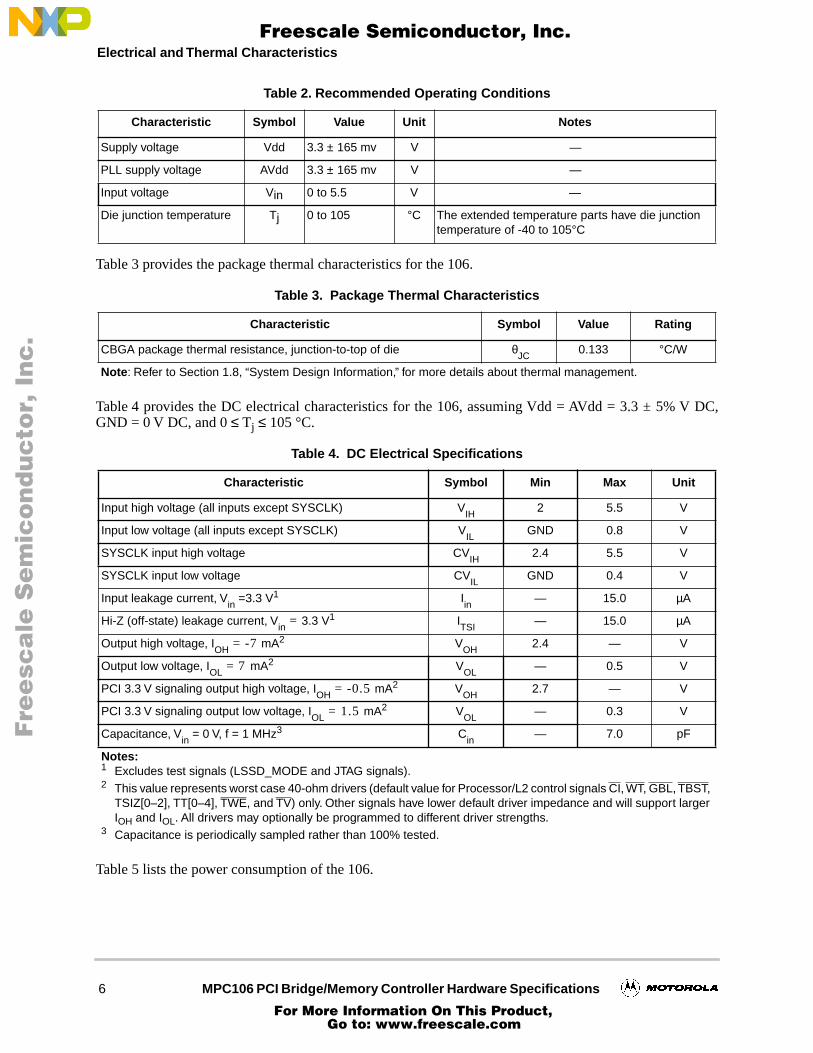
1.4 Electrical and Thermal Characteristics
This section provides both the AC and DC electrical specifications and thermal characteristics for the 106.
1.4.1 DC Electrical Characteristics
The tables in this section describe the 106 DC electrical characteristics. Table 1 provides the absolutemaximum ratings. Functional and tested operating conditions are given in Table 2. Absolute maximumratings are stress ratings only, and functional operation at the maximums is not guaranteed. Stressesbeyond those listed may affect device reliability or cause it permanent damage.
Table 2 provides the recommended operating conditions for the 106. Proper device operation outside ofthese recommended and tested conditions is not guaranteed.
Table 1. Absolute Maximum Ratings
Characteristic Symbol Value Unit Notes
Supply voltage Vdd –0.3 to 3.6 V —
PLL supply voltage AVdd –0.3 to 3.6 V —
Input voltage Vin –0.3 to 5.5 V 1
Junction temperature Tj 0 to 105 °C 2
Storage temperature range Tstg –55 to 150 °C —
Notes
:
1
Caution
: Vin must not exceed Vdd by more than 2.5 V at all times including during power-on reset.
2
The extended temperature parts have die junction temperature of -40 to 105°C. See MPC106ARXTGPNS/D for more information.
Fre
esc
ale
Se
mic
on
du
cto
r, I
Freescale Semiconductor, Inc.
For More Information On This Product, Go to: www.freescale.com
Table 3 provides the package thermal characteristics for the 106.
Table 4 provides the DC electrical characteristics for the 106, assuming Vdd = AVdd = 3.3 ± 5% V DC,GND = 0 V DC, and 0
≤
T
j
≤
105 °C.
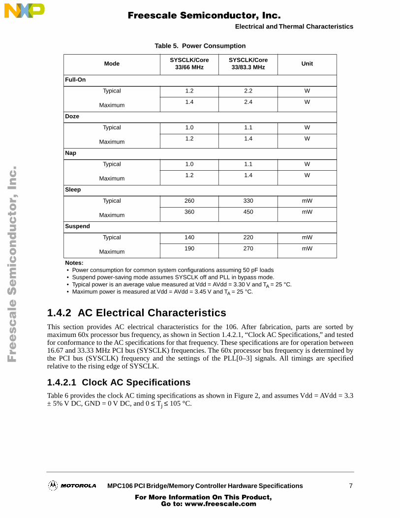
Table 5 lists the power consumption of the 106.
Table 2. Recommended Operating Conditions
Characteristic Symbol Value Unit Notes
Supply voltage Vdd 3.3 ± 165 mv V —
PLL supply voltage AVdd 3.3 ± 165 mv V —
Input voltage Vin 0 to 5.5 V —
Die junction temperature Tj 0 to 105 °C The extended temperature parts have die junction temperature of -40 to 105°C
Table 3. Package Thermal Characteristics
Characteristic Symbol Value Rating
CBGA package thermal resistance, junction-to-top of die
θ
JC
0.133 °C/W
Note
: Refer to Section 1.8, “System Design Information,” for more details about thermal management.
Table 4. DC Electrical Specifications
Characteristic Symbol Min Max Unit
Input high voltage (all inputs except SYSCLK) V
IH
2 5.5 V
Input low voltage (all inputs except SYSCLK) V
IL
GND 0.8 V
SYSCLK input high voltage CV
IH
2.4 5.5 V
SYSCLK input low voltage CV
IL
GND 0.4 V
Input leakage current, V
in
=3.3 V
1
I
in
— 15.0 µA
Hi-Z (off-state) leakage current, V
in
=
3.3 V
1
I
TSI
— 15.0 µA
Output high voltage, I
OH
= -7
mA
2
V
OH
2.4 — V
Output low voltage, I
OL
= 7
mA
2
V
OL
— 0.5 V
PCI 3.3 V signaling output high voltage, I
OH
= -0.5
mA
2
V
OH
2.7 — V
PCI 3.3 V signaling output low voltage, I
OL
= 1.5
mA
2
V
OL
— 0.3 V
Capacitance, V
in
= 0 V, f = 1 MHz
3
C
in
— 7.0 pF
Notes:
1
Excludes test signals (LSSD_MODE and JTAG signals).
2
This value represents worst case 40-ohm drivers (default value for Processor/L2 control signals CI, WT, GBL, TBST, TSIZ[0–2], TT[0–4], TWE, and TV) only. Other signals have lower default driver impedance and will support larger I
OH
and I
OL
. All drivers may optionally be programmed to different driver strengths.
3
Capacitance is periodically sampled rather than 100% tested.
Fre
esc
ale
Se
mic
on
du
cto
r, I
Freescale Semiconductor, Inc.
For More Information On This Product, Go to: www.freescale.com
This section provides AC electrical characteristics for the 106. After fabrication, parts are sorted bymaximum 60x processor bus frequency, as shown in Section 1.4.2.1, “Clock AC Specifications,” and testedfor conformance to the AC specifications for that frequency. These specifications are for operation between16.67 and 33.33 MHz PCI bus (SYSCLK) frequencies. The 60x processor bus frequency is determined bythe PCI bus (SYSCLK) frequency and the settings of the PLL[0–3] signals. All timings are specifiedrelative to the rising edge of SYSCLK.
1.4.2.1 Clock AC Specifications
Table 6 provides the clock AC timing specifications as shown in Figure 2, and assumes Vdd = AVdd = 3.3± 5% V DC, GND = 0 V DC, and 0
≤
T
j
≤
105 °C.
Table 5. Power Consumption
ModeSYSCLK/Core
33/66 MHzSYSCLK/Core33/83.3 MHz
Unit
Full-On
Typical
Maximum
1.2 2.2 W
1.4 2.4 W
Doze
Typical
Maximum
1.0 1.1 W
1.2 1.4 W
Nap
Typical
Maximum
1.0 1.1 W
1.2 1.4 W
Sleep
Typical
Maximum
260 330 mW
360 450 mW
Suspend
Typical
Maximum
140 220 mW
190 270 mW
Notes:
• Power consumption for common system configurations assuming 50 pF loads • Suspend power-saving mode assumes SYSCLK off and PLL in bypass mode. • Typical power is an average value measured at Vdd = AVdd = 3.30 V and T
A
= 25 °C. • Maximum power is measured at Vdd = AVdd = 3.45 V and T
A
= 25 °C.
Fre
esc
ale
Se
mic
on
du
cto
r, I
Freescale Semiconductor, Inc.
For More Information On This Product, Go to: www.freescale.com
Figure 2 provides the SYSCLK input timing diagram.
Figure 2. SYSCLK Input Timing Diagram
1.4.2.2 Input AC Specifications
Table 7 provides the input AC timing specifications for the 106 as defined in Figure 3 and Figure 4. Thesespecifications are for operation between 16.67 and 33.33 MHz PCI bus clock (SYSCLK) frequencies.Assume Vdd = AVdd = 3.3 ± 5% V DC, GND = 0 V DC, and 0
≤
T
j
≤
105 °C.
Table 6. Clock AC Timing Specifications
Num Characteristic
SYSCLK/Core33/66 MHz
SYSCLK/Core33/83.3 MHz Unit Notes
Min Max Min Max
— 60x processor bus (core) frequency 16.67 66 16.67 83.3 MHz 1
— VCO frequency 120 200 120 200 MHz 1, 2
— SYSCLK frequency 16.67 33.33 16.67 33.33 MHz 1
1 SYSCLK cycle time 30.0 60.0 30.0 60.0 ns —
2, 3 SYSCLK rise and fall time — 2.0 — 2.0 ns 3
4 SYSCLK duty cycle measured at 1.4 V 40 60 40 60 % 4
— SYSCLK jitter — ±200 — ±200 ps 5
— 106 internal PLL relock time — 100 — 100
µ
s 4, 6
Notes
:
1
Caution
: The SYSCLK frequency and PLL[0–3] settings must be chosen such that the resulting SYSCLK (bus) frequency, CPU (core) frequency, and PLL (VCO) frequency do not exceed their respective maximum or minimum operating frequencies. Refer to the PLL[0–3] signal description in Section 1.8, “System Design Information,” for valid PLL[0–3] settings, and to Section 1.9, “Document Revision History,” for available frequencies and part numbers.
2
VCO operating range for extended temperature devices is different. Refer to MPC106ARXTGPNS/D for more information.
3
Rise and fall times for the SYSCLK input are measured from 0.4 V to 2.4 V.
4
Timing is guaranteed by design and characterization and is not tested.
5
The total input jitter (short-term and long-term combined) must be under ±200 ps.
6 PLL-relock time is the maximum time required for PLL lock after a stable Vdd, AVdd, and SYSCLK are reached during the power-on reset sequence. This specification also applies when the PLL has been disabled and subsequently re-enabled during the sleep and suspend power-saving modes. Also note that HRST must be held asserted for a minimum of 255 bus clocks after the PLL-relock time (100 µs) during the power-on reset sequence.
VM
VM = Midpoint Voltage (1.4 V)
2 3
CVIL
CVIH
1
SYSCLK VM VM
4 4
Fre
esc
ale
Se
mic
on
du
cto
r, I
Freescale Semiconductor, Inc.
For More Information On This Product, Go to: www.freescale.com
Notes: 1 Input specifications are measured from the TTL level (0.8 or 2.0 V) of the signal in question to the 1.4 V of the rising
edge of SYSCLK. Both input and output timings are measured at the pin (see Figure 3).2 Processor and memory interface signals are specified from the rising edge of the 60x bus clock (which is internally
synchronized to SYSCLK).3 Group I input signals include the following processor, L2, and memory interface signals: A[0–31], PAR[0–7]/AR[1–8],
BR[0–4], BRL2, XATS, LBCLAIM, ADS, BA0, TV and HIT (when configured for external L2)4 Group II input signals include the following processor and memory interface signals: TBST, TT[0–4], TSIZ[0–2], WT,
CI, GBL, AACK, and TA.5 Group III input signals include the following processor and memory interface signals: DL[0–31] and DH[0–31].6 Group IV input signals include the following processor and L2 interface signals: TS, ARTRY, DIRTY_IN, and HIT
(when configured for internal L2 controller).7 PCI 3.3 V signaling environment signals are measured from 1.65 V (Vdd ÷ 2) on the rising edge of SYSCLK to
VOH = 3.0 V or VOL = 0.3 V. PCI 5 V signaling environment signals are measured from 1.65 V (Vdd ÷ 2) on the rising edge of SYSCLK to VOH = 2.4 V or VOL = 0.55 V.
8 Group V input signals include the following bussed PCI interface signals: FRAME, C/BE[0–3], AD[0–31], DEVSEL, IRDY, TRDY, STOP, PAR, PERR, SERR, LOCK, FLSHREQ, and ISA_MASTER.
9 Group VI input signal is the point-to-point PCI GNT input signal. 10 The setup and hold time is with respect to the rising edge of HRST (see Figure 4). Mode select inputs include the
RCS0, FOE, and DBG0 configuration inputs.11 tsysclk is the period of the external clock (SYSCLK) in nanoseconds (ns). When the unit is given as tsysclk, the
numbers given in the table must be multiplied by the period of SYSCLK to compute the actual time duration (in nanoseconds) of the parameter in question.
12 These values are guaranteed by design and are not tested.
Fre
esc
ale
Se
mic
on
du
cto
r, I
Freescale Semiconductor, Inc.
For More Information On This Product, Go to: www.freescale.com
Figure 4 provides the mode select input timing diagram for the 106.
Figure 4. Mode Select Input Timing Diagram
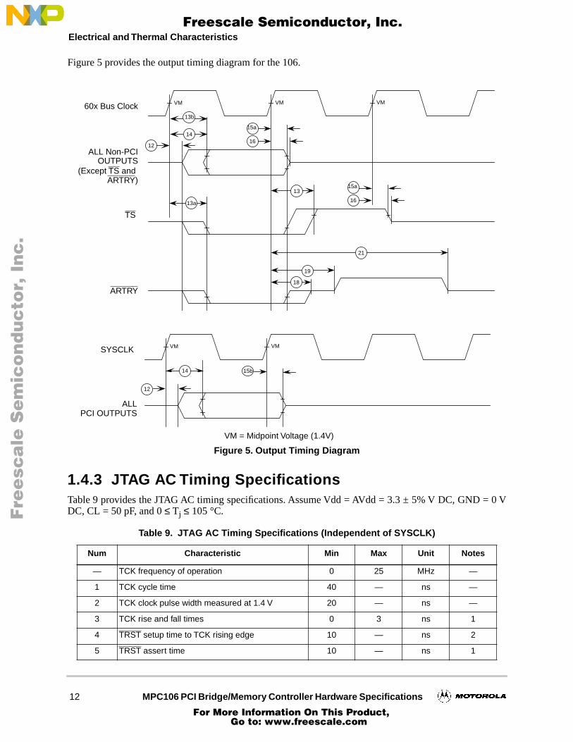
1.4.2.3 Output AC SpecificationsTable 8 provides the output AC timing specifications for 106 (shown in Table 5). Assume Vdd = AVdd =3.3 ± 5% V DC, GND = 0 V DC, CL = 50 pF, and 0 ≤ Tj ≤ 105 °C. Processor and memory interface signalsare specified from the rising edge of the 60x bus clock (which is internally synchronized to SYSCLK). Allunits are nanoseconds.
11a
VM60x Bus Clock
10a
11b
VM
VM = Midpoint Voltage (1.4 V)
SYSCLK
10b
Group I, II, III,
Group V and
and IV INPUTS
VI INPUTS
VM
VM = Midpoint Voltage (1.4 V)
HRST
11c
MODE PINS
10c
Fre
esc
ale
Se
mic
on
du
cto
r, I
Freescale Semiconductor, Inc.
For More Information On This Product, Go to: www.freescale.com
Notes: 1 These values are guaranteed by design and are not tested.2 Output specifications are measured from 1.4 V on the rising edge of the appropriate clock to the TTL level (0.8
V or 2.0 V) of the signal in question. Both input and output timings are measured at the pin (see Figure 5).3 The maximum timing specification assumes CL = 50 pF. 4 The shared outputs TS and ARTRY require pull-up resistors to hold them negated when there is no bus master
driving them.5 When the 106 is configured for asynchronous L2 cache SRAMs, the DWE[0–2] signals have a maximum
SYSCLK to output valid time of (0.5 x tPROC) + 8.0 ns (where tPROC is the 60x bus clock cycle time).6 PCI 3.3 V signaling environment signals are measured from 1.65 V (Vdd ÷ 2) on the rising edge of SYSCLK to
VOH = 3.0 V or VOL = 0.3 V. 7 The minimum timing specification assumes CL = 0 pF. 8 tsysclk is the period of the external bus clock (SYSCLK) in nanoseconds (ns). When the unit is given as tsysclk the
numbers given in the table must be multiplied by the period of SYSCLK to compute the actual time duration (in nanoseconds) of the parameter in question.
9 PCI devices which require more than the PCI-specified hold time of Th = 0ns or systems where clock skew approaches the PCI-specified allowance of 2ns may not work with the MPC106. For workarounds, see Motorola application note Designing PCI 2.1-Compliant MPC106 Systems (order number AN1727/D).
Fre
esc
ale
Se
mic
on
du
cto
r, I
Freescale Semiconductor, Inc.
For More Information On This Product, Go to: www.freescale.com
Figure 6 provides the JTAG clock input timing diagram.
Figure 6. JTAG Clock Input Timing Diagram
Figure 7 provides the TRST timing diagram.
Figure 7. TRST Timing Diagram
6 Boundary-scan input data setup time 5 — ns 3
7 Boundary-scan input data hold time 15 — ns 3
8 TCK to output data valid 0 30 ns 4
9 TCK to output high impedance 0 30 ns 4
10 TMS, TDI data setup time 5 — ns —
11 TMS, TDI data hold time 15 — ns 1
12 TCK to TDO data valid 0 15 ns —
13 TCK to TDO high impedance 0 15 ns —
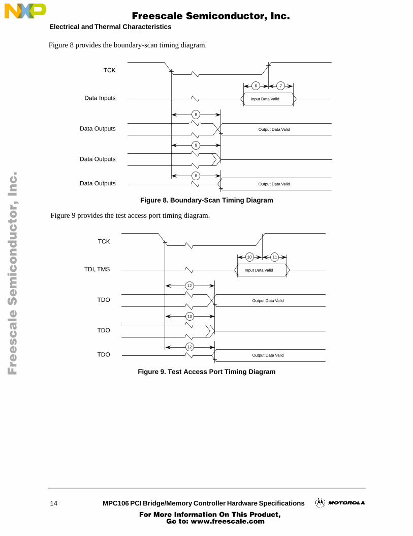
Notes: 1 These values are guaranteed by design, and are not tested2 TRST is an asynchronous signal. The setup time is for test purposes only.3 Non-test signal input timing with respect to TCK.4 Non-test signal output timing with respect to TCK.
Table 9. JTAG AC Timing Specifications (Independent of SYSCLK) (Continued)
Num Characteristic Min Max Unit Notes
TCK
22
1
33
VM = Midpoint Voltage (1.4 V)
VM VM VM
4
5
TRST
TCK
Fre
esc
ale
Se
mic
on
du
cto
r, I
Freescale Semiconductor, Inc.
For More Information On This Product, Go to: www.freescale.com
Note:1 All PCI signals are in little-endian bit order.2 This test signal is for factory use only. It must be pulled up to Vdd for normal device operation.
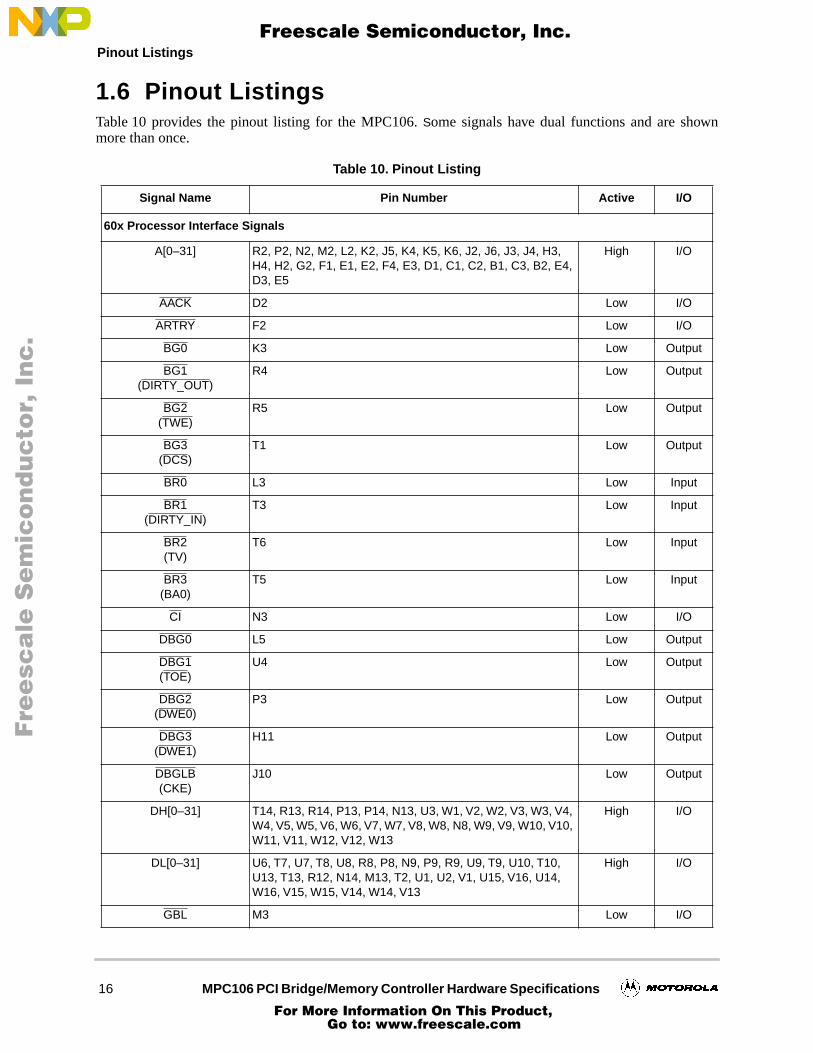
Table 10. Pinout Listing (Continued)
Signal Name Pin Number Active I/O
Fre
esc
ale
Se
mic
on
du
cto
r, I
Freescale Semiconductor, Inc.
For More Information On This Product, Go to: www.freescale.com
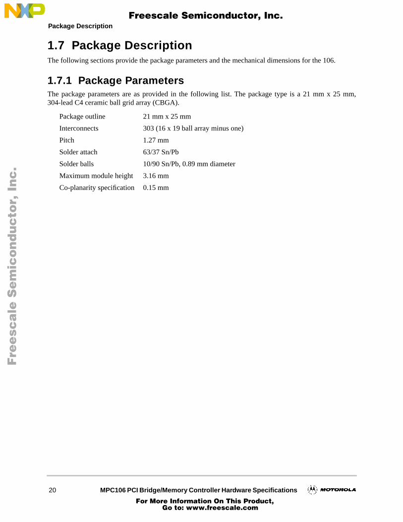
1.7 Package DescriptionThe following sections provide the package parameters and the mechanical dimensions for the 106.
1.7.1 Package ParametersThe package parameters are as provided in the following list. The package type is a 21 mm x 25 mm,304-lead C4 ceramic ball grid array (CBGA).
Package outline 21 mm x 25 mm
Interconnects 303 (16 x 19 ball array minus one)
Pitch 1.27 mm
Solder attach 63/37 Sn/Pb
Solder balls 10/90 Sn/Pb, 0.89 mm diameter
Maximum module height 3.16 mm
Co-planarity specification 0.15 mm
Fre
esc
ale
Se
mic
on
du
cto
r, I
Freescale Semiconductor, Inc.
For More Information On This Product, Go to: www.freescale.com
1.8 System Design InformationThis section provides electrical and thermal design recommendations for successful application of the 106.
1.8.1 PLL ConfigurationThe 106 requires a single system clock input, SYSCLK. The SYSCLK frequency dictates the frequency ofoperation for the PCI bus. An internal PLL on the MPC106 generates a master clock that is used for all ofthe internal (core) logic. The master clock provides the core frequency reference and is phase-locked to theSYSCLK input. The 60x processor, L2 cache, and memory interfaces operate at the core frequency. In the5:2 clock mode (Rev. 4.0 only), the MPC106 needs to sample the 60x bus clock (on the LBCLAIMconfiguration input) to resolve clock phasing with the PCI bus clock (SYSCLK).
The PLL is configured by the PLL[0–3] signals. For a given SYSCLK (PCI bus) frequency, the clock modeconfiguration signals (PLL[0–3]) set the core frequency (and the frequency of the VCO controlling thePLL lock). The supported core and VCO frequencies and the corresponding PLL[0–3] settings areprovided in Table 11.
Notes: 1 PLL[0–3] settings not listed are reserved. Some PLL configurations may select bus, CPU, or VCO frequencies
which are not useful, not supported, or not tested. See Section 1.4.2.1, “Clock AC Specifications,” for valid SYSCLK and VCO frequencies.
2 5:2 clock modes are only supported by MPC106 Rev 4.0; earlier revisions do not support 5:2 clock modes. The 5:2 modes require a 60x bus clock applied to the 60x clock phase (LBCLAIM) configuration input signal during power-on reset, hard reset, and coming out of sleep and suspend power-saving modes.
3 In PLL-bypass mode, the SYSCLK input signal clocks the internal circuitry directly, the PLL is disabled, and the core/SYSCLK ratio is set for 1:1 mode operation. This mode is intended for factory use and third-party tool vendors only. Note also: The AC timing specifications given in this document do not apply in PLL-bypass mode.
4 In clock-off mode, no clocking occurs inside the MPC106 regardless of the SYSCLK input.
Fre
esc
ale
Se
mic
on
du
cto
r, I
Freescale Semiconductor, Inc.
For More Information On This Product, Go to: www.freescale.com
1.8.2 PLL Power Supply FilteringThe AVdd power signal is provided on the 106 to provide power to the clock generation phase-locked loop.To ensure stability of the internal clock, the power supplied to the AVdd input signal should be filteredusing a circuit similar to the one shown in Figure 13. The circuit should be placed as close as possible tothe AVdd pin to ensure it filters out as much noise as possible.
Figure 13. PLL Power Supply Filter Circuit
1.8.3 Decoupling RecommendationsDue to the 106’s large address and data buses and high operating frequencies, it can generate transientpower surges and high frequency noise in its power supply, especially while driving large capacitive loads.This noise must be prevented from reaching other components in the system, and the 106 itself requires aclean, tightly regulated source of power.
It is strongly recommended that the system design include six to eight 0.1 µF (ceramic) and 10 µF(tantalum) decoupling capacitors to provide both high- and low-frequency filtering. These capacitorsshould be placed closely around the perimeter of the 106 package (or on the underside of the PCB). It isalso recommended that these decoupling capacitors receive their power from separate Vdd and GNDpower planes in the PCB, utilizing short traces to minimize inductance. Only surface mount technology(SMT) capacitors should be used to minimize lead inductance.
In addition, it is recommended that there be several bulk storage capacitors distributed around the PCB,feeding the Vdd plane, to enable quick recharging of the smaller chip capacitors. These bulk capacitorsshould have a low equivalent series resistance (ESR) rating to ensure the quick response time necessary.They should also be connected to the power and ground planes through two vias to minimize inductance.Suggested bulk capacitors—100 µF (AVX TPS tantalum) or 330 µF (AVX TPS tantalum).
1.8.4 Connection RecommendationsTo ensure reliable operation, it is recommended to connect unused inputs to an appropriate signal level.Unused active low inputs should be tied (using pull-up resistors) to Vdd. Unused active high inputs shouldbe tied (using pull-down resistors) to GND. All no-connect (NC) signals must remain unconnected.
Power and ground connections must be made to all external Vdd, AVdd, and GND pins of the 106.
1.8.4.1 Pull-up Resistor RecommendationsThe MPC106 requires pull-up (or pull-down) resistors on several control signals of the 60x and PCI busesto maintain the control signals in the negated state after they have been actively negated and released by the106 or other bus masters. The JTAG test reset signal, TRST, should be pulled down during normal systemoperation. Also, as indicated in Table 10, the factory test signal, LSSD_MODE, must be pulled up fornormal device operation
During inactive periods on the bus, the address and transfer attributes on the bus (A[0–31], TT[0–4],TBST, WT, CI, and GBL) are not driven by any master and may float in the high-impedance state forrelatively long periods of time. Since the MPC106 must continually monitor these signals, this float
Vdd AVdd10 Ω
10 µF 0.1 µF
GND
(3.3 V)
Fre
esc
ale
Se
mic
on
du
cto
r, I
Freescale Semiconductor, Inc.
For More Information On This Product, Go to: www.freescale.com
condition may cause excessive power draw by the input receivers on the MPC106 or by other receivers inthe system. It is recommended that these signals be pulled up or restored in some manner by the system.
The 60x data bus input receivers on the MPC106 do not require pull-up resistors on the data bus signals(DH[0–31], DL[0–31], and PAR[0–7]). However, other data bus receivers in the system may requirepull-up resistors on these signals.
In general, the 60x address and control signals are pulled up to 3.3 VDC and the PCI control signals arepulled up to 5 VDC through weak (2–10 kΩ) resistors. Resistor values may need to be adjusted stronger toreduce induced noise on specific board designs. Table 12 summarizes the pull-up/pull-downrecommendations for the MPC106.
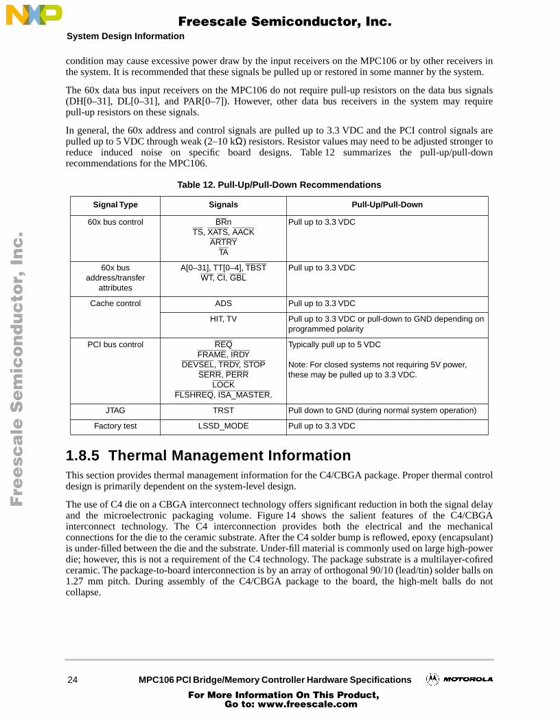
1.8.5 Thermal Management InformationThis section provides thermal management information for the C4/CBGA package. Proper thermal controldesign is primarily dependent on the system-level design.
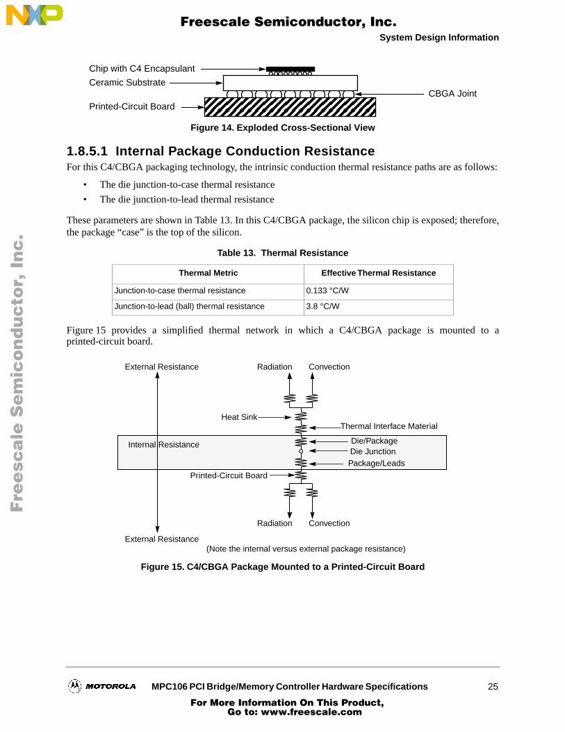
The use of C4 die on a CBGA interconnect technology offers significant reduction in both the signal delayand the microelectronic packaging volume. Figure 14 shows the salient features of the C4/CBGAinterconnect technology. The C4 interconnection provides both the electrical and the mechanicalconnections for the die to the ceramic substrate. After the C4 solder bump is reflowed, epoxy (encapsulant)is under-filled between the die and the substrate. Under-fill material is commonly used on large high-powerdie; however, this is not a requirement of the C4 technology. The package substrate is a multilayer-cofiredceramic. The package-to-board interconnection is by an array of orthogonal 90/10 (lead/tin) solder balls on1.27 mm pitch. During assembly of the C4/CBGA package to the board, the high-melt balls do notcollapse.
Table 12. Pull-Up/Pull-Down Recommendations
Signal Type Signals Pull-Up/Pull-Down
60x bus control BRnTS, XATS, AACK
ARTRYTA
Pull up to 3.3 VDC
60x bus address/transfer
attributes
A[0–31], TT[0–4], TBSTWT, CI, GBL
Pull up to 3.3 VDC
Cache control ADS Pull up to 3.3 VDC
HIT, TV Pull up to 3.3 VDC or pull-down to GND depending on programmed polarity
PCI bus control REQFRAME, IRDY
DEVSEL, TRDY, STOPSERR, PERR
LOCKFLSHREQ, ISA_MASTER.
Typically pull up to 5 VDC
Note: For closed systems not requiring 5V power, these may be pulled up to 3.3 VDC.
JTAG TRST Pull down to GND (during normal system operation)
Factory test LSSD_MODE Pull up to 3.3 VDC
Fre
esc
ale
Se
mic
on
du
cto
r, I
Freescale Semiconductor, Inc.
For More Information On This Product, Go to: www.freescale.com
1.8.5.2 Board and System-Level ModelingA common figure-of-merit used for comparing the thermal performance of various microelectronicpackaging technologies is the junction-to-ambient thermal resistance. The final chip-junction operatingtemperature is not only a function of the component-level thermal resistance, but the system-level designand its operating conditions. In addition to the component’s power consumption, a number of factors affectthe final operating die-junction temperature. For example, these factors might include airflow, boardpopulation, heat sink efficiency, heat sink attach, next-level interconnect technology, and system airtemperature rise.
Due to the complexity and the many variations of system-level boundary conditions for today’smicroelectronic equipment, the combined effects of the heat transfer mechanisms (radiation, convection,and conduction) may vary widely. For this reason, we recommend using conjugate heat transfer models forthe board as well as system-level designs. To expedite system-level thermal analysis, several “compact”CBGA thermal models are available on request within FLOTHERM®.
The die junction-to-ambient thermal resistance is shown in Table 14. The model results are in accordancewith SEMI specification G38. This standard specifies a single component be placed on a 7.5 cm x 10 cmsingle-layer printed-circuit card. Note that this single metric may not adequately describethree-dimensional heat flow.
Table 14. Die Junction-to-Ambient Thermal Resistance
Airflow Velocity (Meter/Second)
Airflow Velocity(Feet/Minute)
Die Junction-to-Ambient Thermal Resistance (SEMI G38) (°C/W)
1 196.8 22.0
2 393.7 18.5
3 590.0 17.0
Fre
esc
ale
Se
mic
on
du
cto
r, I
Freescale Semiconductor, Inc.
For More Information On This Product, Go to: www.freescale.com
1.9 Document Revision HistoryTable 15 lists significant changes between revisions of this document.
Table 15. Document Revision History
Document Revision
Substantive Change(s)
Rev 0 Initial release
Rev 1 Changed VCO maximum frequency in Table 6 to 200 MHz
Changed input and Hi-Z leakage current in Table 4. from 10µA to 15µA
Changed IOH
and IOL
in Table 4 from 18mA and 14mA respectively to -7mA and 7mA to correct the sign and reduce the current to worst case value for the lowest strength default driver
Changed footnote 4 to Table 6 to be consistent with SYSCLK jitter spec of 200ps
Modified Table 7, Figure 3, Table 8, and Figure 5 to clarify reference clock (60x Bus Clock or SYSCLK) for input and output specifications
Changed Group I and Group II signals input setup requirement for 83 MHz in Table 7 from 3.0 ns to 3.5 ns min.
Changed Group I-IV (non-PCI signals) input hold requirement (Spec 11a) in Table 7 from 1.0 ns to 0 ns
Changed Group V and VI (PCI signals) input hold requirement (Spec 11b) in Table 7 from 1.0ns to -0.5ns
Changed output valid times for all non-PCI signals (Specs 13a, 13b and 14a) from 8 ns to 7 ns at 66 Mhz and from 7 ns to 6 ns at 83 MHz
Corrected Figure 10 to reflect TOE signal is shared with DBG1 on pin U5
Rev 2 Changed input and Hi-Z leakage current, Vin in Table 4 from 5.5V to 3.3V
Changed the power consumption data in Table 5
Changed note 7 of Table 8 to show the minimum timing specification assumes CL=0 pF
Rev 3 Deleted PLL[0-3] = 0010 from Table 11 to remove 1:1 mode operation between 16MHz and 25MHz
Added note 10 to Table 8 regarding PCI hold time
Lowered PCI 3.3V signalling output high voltage from 3.0 V to 2.7V and added current conditions for PCI 3.3V VOH and VOL in Table 4 to reflect current production test
Included note 12 in Specification 10c of Table 4; Clarified note 9 in Table 8 and included in Specification 12 and 18; Added a similar “guaranteed by design and not tested” note to Table 9 and included in Specifications 3, 7, and 11. All to reflect current production test.
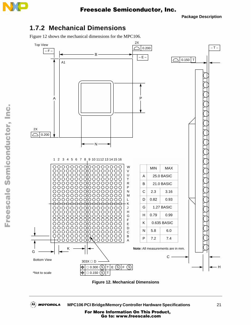
Corrected Figure 12 dimensions from TBD to actual die size
Table 1 and Table 2 include notes on extended temperature parts.
Rev 4 Table 8, Note 8 changed to include: “These values are guaranteed by design and are not tested.”
Rev 5 Added PNS references below Table 1 and Table 6. Changed footnote ordering in Table 8, Table 9, and Table 10. Added new footnote 2 to Table 6. Changed part number key.
Fre
esc
ale
Se
mic
on
du
cto
r, I
Freescale Semiconductor, Inc.
For More Information On This Product, Go to: www.freescale.com
nc
...
Information in this document is provided solely to enable system and software implementers to use PowerPC microprocessors. There are no expressor implied copyright licenses granted hereunder to design or fabricate PowerPC integrated circuits or integrated circuits based on the information inthis document.Motorola reserves the right to make changes without further notice to any products herein. Motorola makes no warranty, representation or guaranteeregarding the suitability of its products for any particular purpose, nor does Motorola assume any liability arising out of the application or use of anyproduct or circuit, and specifically disclaims any and all liability, including without limitation consequential or incidental damages. “Typical” parameterswhich may be provided in Motorola data sheets and/or specifications can and do vary in different applications and actual performance may vary overtime. All operating parameters, including “Typicals” must be validated for each customer application by customer’s technical experts. Motorola doesnot convey any license under its patent rights nor the rights of others. Motorola products are not designed, intended, or authorized for use ascomponents in systems intended for surgical implant into the body, or other applications intended to support or sustain life, or for any other applicationin which the failure of the Motorola product could create a situation where personal injury or death may occur. Should Buyer purchase or use Motorolaproducts for any such unintended or unauthorized application, Buyer shall indemnify and hold Motorola and its officers, employees, subsidiaries,affiliates, and distributors harmless against all claims, costs, damages, and expenses, and reasonable attorney fees arising out of, directly or indirectly,any claim of personal injury or death associated with such unintended or unauthorized use, even if such claim alleges that Motorola was negligentregarding the design or manufacture of the part. Motorola and are registered trademarks of Motorola, Inc. Motorola, Inc. is an EqualOpportunity/Affirmative Action Employer.
HOW TO REACH US:USA/EUROPE/LOCATIONS NOT LISTED: Motorola Literature Distribution; P.O. Box 5405, Denver, Colorado 80217. 1-303-675-2140 or1-800-441-2447JAPAN: Motorola Japan Ltd.; SPS, Technical Information Center, 3-20-1, Minami-Azabu. Minato-ku, Tokyo 106-8573 Japan. 81-3-3440-3569ASIA/PACIFIC: Motorola Semiconductors H.K. Ltd.; Silicon Harbour Centre, 2 Dai King Street, Tai Po Industrial Estate, Tai Po, N.T., Hong Kong.852-26668334TECHNICAL INFORMATION CENTER: 1-800-521-6274HOME PAGE: http://www.motorola.com/semiconductorsDOCUMENT COMMENTS: FAX (512) 933-2625, Attn: RISC Applications EngineeringWORLD WIDE WEB ADDRESSES: http://www.motorola.com/PowerPC
DigitalDNA is a trademark of Motorola, Inc.The PowerPC name, the PowerPC logotype, and PowerPC 603e are trademarks of International Business Machines Corporation used by Motorolaunder license from International Business Machines Corporation.
1.10 Ordering InformationFigure 16 provides the Motorola part-numbering nomenclature for the 106. In addition to the corefrequency, the part numbering scheme also consists of a part modifier and application modifier. The partmodifier indicates any enhancements in the part from the original production design. The applicationmodifier may specify special bus frequencies or application conditions. Each part number also contains arevision code. This refers to the die mask revision number and is specified in the part-numbering schemefor identification purposes only.
pr
MPC 106 A RX xx x xProduct Code Part Identifier Part Modifier Package Frequency Application Modifier Revision Level2
RX = BGA 66 or 83 C No 5:2 modeD 5:2 modeT Extended temperature1
E 3.0G 4.0
Notes: 1 See Part Number Specifications (MPC106ARXTGPNS/D).2 For current revision level, contact local Motorola sales office.
Figure 16. Part Number Key
Fre
esc
ale
Se
mic
on
du
cto
r, I
Freescale Semiconductor, Inc.
For More Information On This Product, Go to: www.freescale.com