Issue date: May 2001Status: NewVersion: 2.3Revision: 00
COPYRIGHT
WE RESERVE ALL RIGHTS TO THIS DOCUMENT, EVEN IN THE EVENT THAT A PATENT IS ISSUED AND A DIFFERENT COMMERCIAL PROPRIETARY RIGHT IS REGISTERED. IMPROPER USE, IN PARTICULAR REPRODUCTION AND DIS-SEMINATION TO THIRD PARTIES, IS NOT PERMITTED.
THIS DOCUMENT HAS BEEN CAREFULLY CHECKED. IF THE USER NEVERTHELESS DETECTS ANY ERRORS, HE IS ASKED TO NOTIFY US AS SOON AS POSSIBLE.
THE DATA CONTAINED IN THIS MANUAL IS INTENDED SOLELY FOR THE PRODUCT DESCRIPTION AND IS NOT TO BE DEEMED TO BE A STATEMENT OF GUARANTEED PROPERTIES. IN THE INTERESTS OF OUR CUSTOMERS, WE CON-STANTLY SEEK TO ENSURE THAT OUR PRODUCTS ARE DEVELOPED TO THE LATEST TECHNOLOGICAL STAN-DARDS. AS A RESULT, IT IS POSSIBLE THAT THERE MAY BE SOME DIFFERENCES BETWEEN THE HW/SW PRODUCT AND THIS INFORMATION PRODUCT.
Introduction to the technical reference manual.................................... 2About the complete set of manuals to a terminal............................ 2Design of the Technical reference manual (TRM).......................... 3Related documents......................................................................... 6
Logic diagram ............................................................................... 33Input and output signals................................................................ 35Technical data .............................................................................. 35
Logic function blocks ......................................................................... 36Application .................................................................................... 36Inverter function block (INV) ......................................................... 36OR function block (OR)................................................................. 37AND function block (AND) ............................................................ 37Timer function block (TM) ............................................................. 38Timer long function block (TL) ...................................................... 39Pulse timer function block (TP)..................................................... 40Extended length pulse function block (TQ)................................... 41Exclusive OR function block (XO)................................................. 41Set-reset function block (SR)........................................................ 42Set-reset with memory function block (SM) .................................. 43Controllable gate function block (GT) ........................................... 43Settable timer function block (TS)................................................. 44Move first function block (MOF).................................................... 45Move last function block (MOL) .................................................... 46Technical data .............................................................................. 47
Blocking of signals during test ........................................................... 48Application .................................................................................... 48Function block............................................................................... 48Input and output signals................................................................ 48
Chapter 4 Line impedance ............................................................. 49
Pole slip protection (PSP) .................................................................. 50Application .................................................................................... 50Functionality.................................................................................. 50Function block............................................................................... 51Logic diagram ............................................................................... 51Input and output signals................................................................ 59Setting parameters ....................................................................... 60Technical data .............................................................................. 63
Chapter 5 Current ........................................................................... 65
Chapter 7 Power system supervision ......................................... 127
Loss of voltage check (LOV)............................................................ 128Application .................................................................................. 128
Contents
Functionality ............................................................................... 128Function block ............................................................................ 128Logic diagram ............................................................................. 129Input and output signals ............................................................. 129Setting parameters ..................................................................... 130Technical data ............................................................................ 130
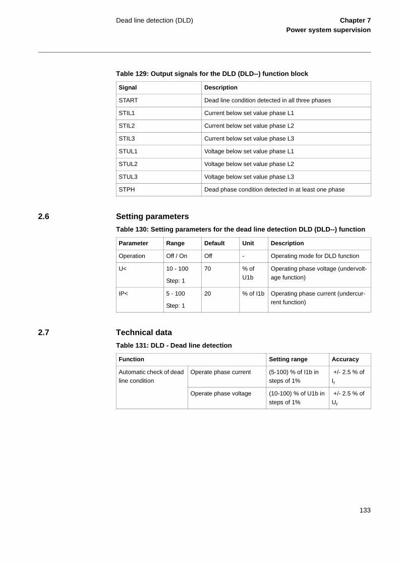
Dead line detection (DLD) ............................................................... 131Application .................................................................................. 131Functionality ............................................................................... 131Function block ............................................................................ 131Logic diagram ............................................................................. 132Input and output signals ............................................................. 132Setting parameters ..................................................................... 133Technical data ............................................................................ 133
Chapter 8 Secondary system supervision ................................. 135
Pole discordance protection (PD) .................................................... 306Application .................................................................................. 306Functionality................................................................................ 306Function block............................................................................. 306Logic diagram ............................................................................. 307Input and output signals.............................................................. 307Setting parameters ..................................................................... 308Technical data ............................................................................ 308
Binary signal transfer to remote end (RTC) ..................................... 309General ....................................................................................... 309Application .................................................................................. 309Functionality................................................................................ 309Function block............................................................................. 310Input and output signals.............................................................. 311Setting parameters ..................................................................... 311
Serial communication....................................................................... 312Application, common .................................................................. 312Design, common......................................................................... 312
Serial communication, SPA (SPA-bus V 2.4 protocol)..................... 314Application .................................................................................. 314Design......................................................................................... 314Setting parameters ..................................................................... 314Technical data ............................................................................ 315
Serial communication, IEC (IEC 60870-5-103 protocol) .................. 316Application .................................................................................. 316Design......................................................................................... 316IEC 60870-5-103 information types ............................................ 316Function block............................................................................. 323Input and output signals.............................................................. 323Setting parameters ..................................................................... 324Technical data ............................................................................ 324
Serial communication, LON ............................................................. 325Application .................................................................................. 325Design......................................................................................... 325Technical data ............................................................................ 325
Contents
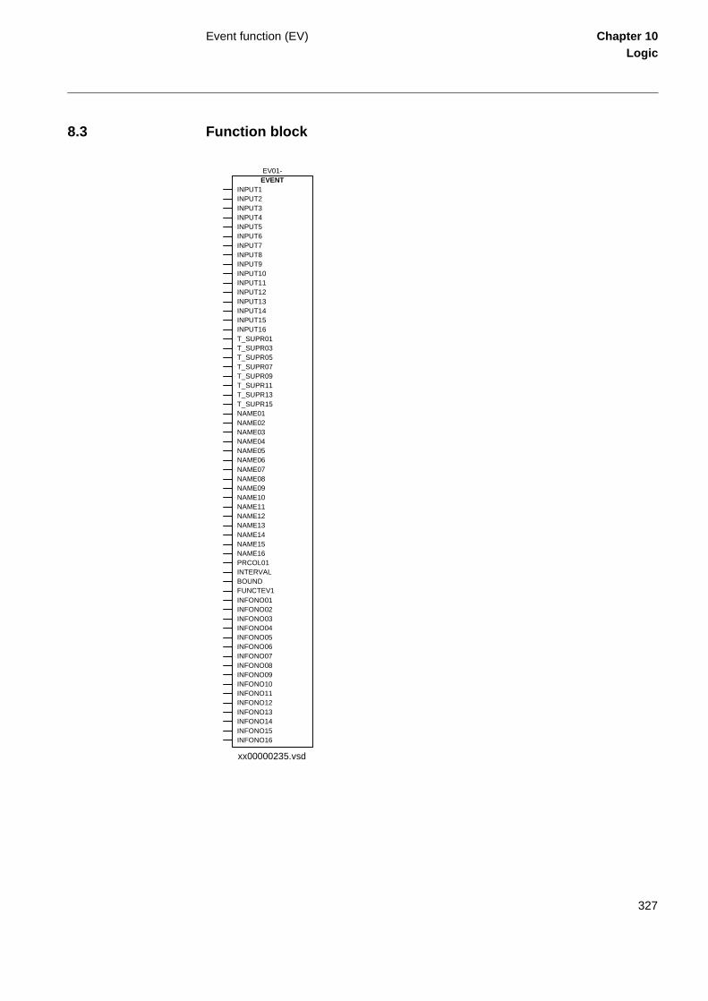
Event function (EV).......................................................................... 326Application .................................................................................. 326Design ........................................................................................ 326Function block ............................................................................ 327Input and output signals ............................................................. 328Setting parameters ..................................................................... 329
Design......................................................................................... 376Technical data ............................................................................ 376
mA input module (MIM).................................................................... 387Application .................................................................................. 387Design......................................................................................... 387
Contents
Function block ............................................................................ 387Technical data ............................................................................ 387
Power supply module (PSM) ........................................................... 388Application .................................................................................. 388Design ........................................................................................ 388Function block ............................................................................ 388Input and output signals ............................................................. 389Technical data ............................................................................ 389
Serial communication modules (SCM) ............................................ 403Design, SPA/IEC ........................................................................ 403Design, LON ............................................................................... 403Technical data ............................................................................ 403
Data communication modules ......................................................... 404Application .................................................................................. 404Technical data ............................................................................ 405
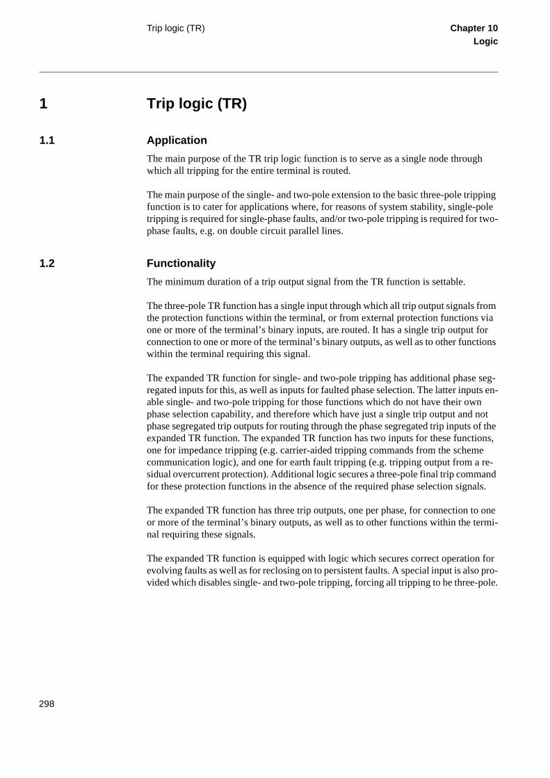
This chapter introduces you to the manual as such.
1
Introduction to the technical reference manual
Chapter 1Introduction
es or on of
refer-l and
nfig-ters n
1 Introduction to the technical reference manual
1.1 About the complete set of manuals to a terminal
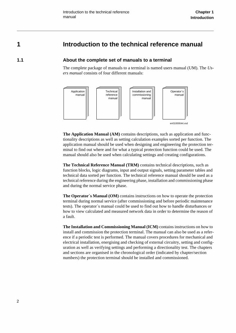
The complete package of manuals to a terminal is named users manual (UM). The Us-ers manual consists of four different manuals:
The Application Manual (AM) contains descriptions, such as application and func-tionality descriptions as well as setting calculation examples sorted per function. The application manual should be used when designing and engineering the protection ter-minal to find out where and for what a typical protection function could be used. The manual should also be used when calculating settings and creating configurations.
The Technical Reference Manual (TRM) contains technical descriptions, such as function blocks, logic diagrams, input and output signals, setting parameter tables and technical data sorted per function. The technical reference manual should be used as a technical reference during the engineering phase, installation and commissioning phase and during the normal service phase.
The Operator´s Manual (OM) contains instructions on how to operate the protection terminal during normal service (after commissioning and before periodic maintenance tests). The operator´s manual could be used to find out how to handle disturbanchow to view calculated and measured network data in order to determine the reasa fault.
The Installation and Commissioning Manual (ICM) contains instructions on how toinstall and commission the protection terminal. The manual can also be used as aence if a periodic test is performed. The manual covers procedures for mechanicaelectrical installation, energising and checking of external circuitry, setting and couration as well as verifying settings and performing a directionality test. The chapand sections are organised in the chronological order (indicated by chapter/sectionumbers) the protection terminal should be installed and commissioned.
Applicationmanual
Technicalreference
manual
Installation andcommissioning
manual
Operator´smanual
en01000044.vsd
2
Introduction to the technical reference manual
Chapter 1Introduction
1.2 Design of the Technical reference manual (TRM)
The description of each terminal related function follows the same structure (where ap-plicable):
Application
States the most important reasons for the implementation of a particular protection function.
Functionality/Design
Presents the general concept of a function.
Function block
Each function block is imaged by a graphical symbol.
Input signals are always on the left side, and output signals on the right side. Settings are not displayed. A special kind of settings are sometimes available. These are sup-posed to be connected to constants in the configuration scheme, and are therefore de-picted as inputs. Such signals will be found in the signal list but described in the settings table.
Figure 1: Function block symbol example
Logic diagram
The description of the design is chiefly based on simplified logic diagrams, which use IEC symbols, for the presentation of different functions, conditions etc. The functions are presented as a closed block with the most important internal logic circuits and con-figurable functional inputs and outputs.
Completely configurable binary inputs/outputs and functional inputs/outputs enable the user to prepare the REx 5xx with his own configuration of different functions, accord-ing to application needs and standard practice.
TUVBLOCKBLKTRVTSU
TRIPSTL1STL2STL3
START
xx00000207.vsd
3
Introduction to the technical reference manual
Chapter 1Introduction
d Un-
ill (1).
pos-s to V-ide re-me.
ir log- sig-e for
Figure 2: Function block diagram example
The names of the configurable logic signals consist of two parts divided by dashes. The first part consists of up to four letters and presents the abbreviated name for the corre-sponding function. The second part presents the functionality of the particular signal. According to this explanation, the meaning of the signal TUV--BLKTR is as follows.
• The first part of the signal, TUV- represents the adherence to the Time delayeder-Voltage function.
• The second part of the signal name, BLKTR informs the user that the signal wBLocK the TRip from the under-voltage function, when its value is a logical one
Different binary signals have special symbols with the following significance:
• Signals drawn to the box frame to the left present functional input signals. It issible to configure them to functional output signals of other functions as well abinary input terminals of the REx 5xx terminal. Examples are TUV--BLKTR, TU-BLOCK and TUV--VTSU.Signals in frames with a shaded area on their right spresent the logical setting signals. Their values are high (1) only when the corsponding setting parameter is set to the symbolic value specified within the fraExample is the signal Operation = On. These signals are not configurable. Theical values correspond automatically to the selected setting value.The internalnals are usually dedicated to a certain function. They are normally not availabl
TUV--BLKTR
TUV--BLOCK
TUV--VTSU >1
STUL1
STUL2
&
&
&STUL3
Operation = On
>1& t
tt
15 msTUV--TRIP
TUV--START
TUV--STL1
TUV--STL2
TUV--STL3
t15 ms
t15 ms
t15 ms
t15 ms
TRIP - cont.
xx01000170.vsd
4
Introduction to the technical reference manual
Chapter 1Introduction
configuration purposes. Examples in are signals STUL1, STUL2 and STUL3.The functional output signals, drawn to the box frame to the right, present the logical out-puts of functions and are available for configuration purposes. The user can config-ure them to binary outputs from the terminal or to inputs of different functions. Typical examples in are signals TUV--TRIP, TUV--START etc.
Other internal signals configurated to other function blocks are written on a line with an identity and a cont. reference. An example is the signal TRIP - cont. The signal can be found in the corresponding function with the same identity.
Input and output signals
The signal lists contain all available input and output signals of the function block, one table for input signals and one for output signals.
Table 1: Input signals for the TUV (TUV--) function block
Table 2: Output signals for the TUV (TUV--) function block
Setting parameters
The setting parameters table contains all available settings of the function block. If a function consists of more than one block, each block is listed in a separate table.
Signal Description
BLOCK Block undervoltage function
BLKTR Block of trip from time delayed undervoltage function
VTSU Block from voltage transformer circuit supervision
Signal Description
TRIP Trip by time delayed undervoltage function
STL1 Start phase undervoltage phase L1
STL2 Start phase undervoltage phase L2
STL3 Start phase undervoltage phase L3
START Start phase undervoltage
5
Introduction to the technical reference manual
Chapter 1Introduction
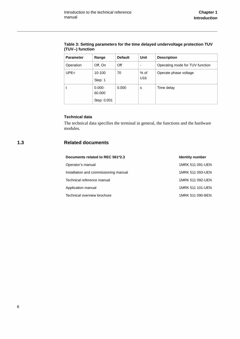
Table 3: Setting parameters for the time delayed undervoltage protection TUV (TUV--) function
Technical data
The technical data specifies the terminal in general, the functions and the hardware modules.
1.3 Related documents
Parameter Range Default Unit Description
Operation Off, On Off - Operating mode for TUV function
UPE< 10-100
Step: 1
70 % of U1b
Operate phase voltage
t 0.000-
60.000
Step: 0.001
0.000 s Time delay
Documents related to REC 561*2.3 Identity number
Operator’s manual 1MRK 511 091-UEN
Installation and commissioning manual 1MRK 511 093-UEN
Technical reference manual 1MRK 511 092-UEN
Application manual 1MRK 511 101-UEN
Technical overview brochure 1MRK 511 090-BEN
6
About this chapter Chapter 2General
Chapter 2 General
About this chapter
This chapter describes the terminal in general.
7
Terminal identification Chapter 2General
1 Terminal identification
1.1 General terminal parameters
Use the terminal identifiers to name the individual terminal for identification purposes. Use the terminal reports to check serial numbers of the terminal and installed modules and to check the firmware version.
Identifiers and reports are accessible by using the HMI as well as by SMS or SCS sys-tems.
Table 4: Set parameters for the general terminal parameters function
1.2 Basic protection parameters
Path in HMI-tree: Configuration/AnalogInputs/General
Table 5: Setting parameters for analogInputs - General
Path in HMI-tree: Configuration/AnalogInputs/U1-U5
Parameter Range Default Unit Description
Station Name 0-16 Station
Name
char Identity name for the station
Station No 0-99999 0 - Identity number for the station
Object Name 0-16 Object
Name
char Identity name for the protected
object
Object No 0-99999 0 - Identity number for the protected object
Unit Name 0-16 Unit Name char Identity name for the terminal
Unit No 0-99999 0 - Identity number for the terminal
Parameter Range Default Unit Description
CTEarth In/Out Out - Direction of CT earthing
fr 50, 60, 16 2/3
50 Hz System frequency
8
Terminal identification Chapter 2General
Table 6: Analog Inputs - Voltage
Parameter Range Default Unit Description
U1r * 10.000 - 500.000
Step: 0.001
63.509 V Rated voltage of transformer on input U1
U1b 30.000 -
500.000
Step:0.001
63.509 V Base voltage of input U1
U1Scale 1.000 - 20000.000
Step: 0.001
2000.000 - Main voltage transformer ratio, input U1
Name_U1 0 - 13 U1 char User-defined name of input U1
U2r * 10.000 - 500.000
Step: 0.001
63.509 V Rated voltage of transformer on input U2
U2b 30.000 - 500.000
Step: 0.001
63.509 V Base voltage of input U2
U2Scale 1.000 -
20000.000
Step: 0.001
2000.000 - Main voltage transformer ratio, input
U2
Name_U2 0 - 13 U2 char User-defined name of input U2
U3r * 10.000 -
500.000
Step: 0.001
63.509 V Rated voltage of transformer on
input U3
U3b 30.000 - 500.000
Step: 0.001
63.509 V Base voltage of input U3
U3Scale 1.000 - 20000.000
Step: 0.001
2000.000 - Main voltage transformer ratio, input U3
Name_U3 0 - 13 U3 char User-defined name of input U3
9
Terminal identification Chapter 2General
Path in HMI-tree: Configuration/AnalogInputs/I1-I5
U4r * 10.000 -
500.000
Step: 0.001
63.509 V Rated voltage of transformer on
input U4
U4b 30.000 -
500.000
Step: 0.001
63.509 V Base voltage of input U4
U4Scale 1.000 - 20000.000
Step: 0.001
2000.000 - Main voltage transformer ratio, input U4
Name_U4 0 - 13 U4 char User-defined name of input U4
U5r * 10.000 - 500.000
Step: 0.001
63.509 V Rated voltage of transformer on input U5
U5b 30.000 - 500.000
Step: 0.001
63.509 V Base voltage of input U5
U5Scale 1.000 -
20000.000
Step: 0.001
2000.000 - Main voltage transformer ratio, input
U5
Name_U5 0 - 13 U5 char User-defined name of input U5
*) Setting is done through the local HMI only.
Parameter Range Default Unit Description
10
Terminal identification Chapter 2General
Table 7: Analog Inputs - Current
Parameter Range Default Unit Description
I1r * 0.1000 - 10.0000
Step: 0.0001
1.0000 A Rated current of transformer on input I1
I1b 0.1 - 10.0
Step: 0.1
1.0 A Base current of input I1
I1Scale 1.000 - 40000.000
Step: 0.001
2000.000 - Main current transformer ratio, input I1
Name_I1 0 - 13 I1 char User-defined name of input I1
I2r * 0.1000 - 10.0000
Step:
0.0001
1.0000 A Rated current of transformer on input I2
I2b 0.1 - 10.0
Step: 0.1
1.0 A Base current of input I2
I2Scale 1.000 -
40000.000
Step:0.001
2000.000 - Main current transformer ratio,
input I2
Name_I2 0 - 13 I2 char User-defined name of input I2
I3r * 0.1000 -
10.0000
Step: 0.0001
1.0000 A Rated current of transformer on
input I3
I3b 0.1 - 10.0
Step: 0.1
1.0 A Base current of input I3
I3Scale 1.000 - 40000.000
Step: 0.001
2000.000 - Main current transformer ratio, input I3
Name_I3 0 - 13 I3 char User-defined name of input I3
11
Terminal identification Chapter 2General
1.3 Calendar and clock
Table 8: Calendar and clock
I4r * 0.1000 -
10.0000
Step: 0.0001
1.0000 A Rated current of transformer on
input I4
I4b 0.1 - 10.0
Step: 0.1
1.0 A Base current of input I4
I4Scale 1.000 - 40000.000
Step: 0.001
2000.000 - Main current transformer ratio, input I4
Name_I4 0 - 13 I4 char User-defined name of input I4
I5r * 0.1000 - 10.0000
Step:
0.0001
1.0000 A Rated current of transformer on input I5
I5b 0.1 - 10.0
Step: 0.1
1.0 A Base current of input I5
I5Scale 1.000 -
40000.000
Step: 0.001
2000.000 - Main current transformer ratio,
input I5
Name_I5 0 - 13 I5 char User-defined name of input I5
*) Setting is done through the local HMI only
Parameter Range Default Unit Description
Parameter Range
Built-in calender 30 years with leap years
12
Technical data Chapter 2General
2 Technical data
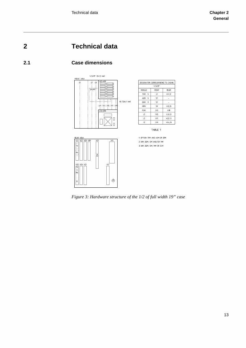
2.1 Case dimensions
Figure 3: Hardware structure of the 1/2 of full width 19” case
13
Technical data Chapter 2General
Figure 4: Hardware structure of the 3/4 of full width 19” case
14
Technical data Chapter 2General
Figure 5: Hardware structure of the full width 19” case
E = 187.6 mm without protection cover, 228.6 mm with protection cover
F = 106.5 mm
G = 97.6 mm without protection cover, 138.6 mm with protection cover
17
Technical data Chapter 2General
The flush mounting kits are available in three designs, suitable for 1/2, 3/4 or full width terminals and consists of four fasteners (4) with appropriate mounting details and a seal-ing strip (1) providing IP54 class protection for fastening to the terminal (5). The semi-flush mounting kit adds a distance frame (2). An additional sealing strip (3) can be ordered for semiflush mounting to provide IP54 class protection.
Figure 6: The flush mounting kit
xx00000129.eps
12
3
4
56
xx01000049.vsden01000047.vsd
18
Technical data Chapter 2General
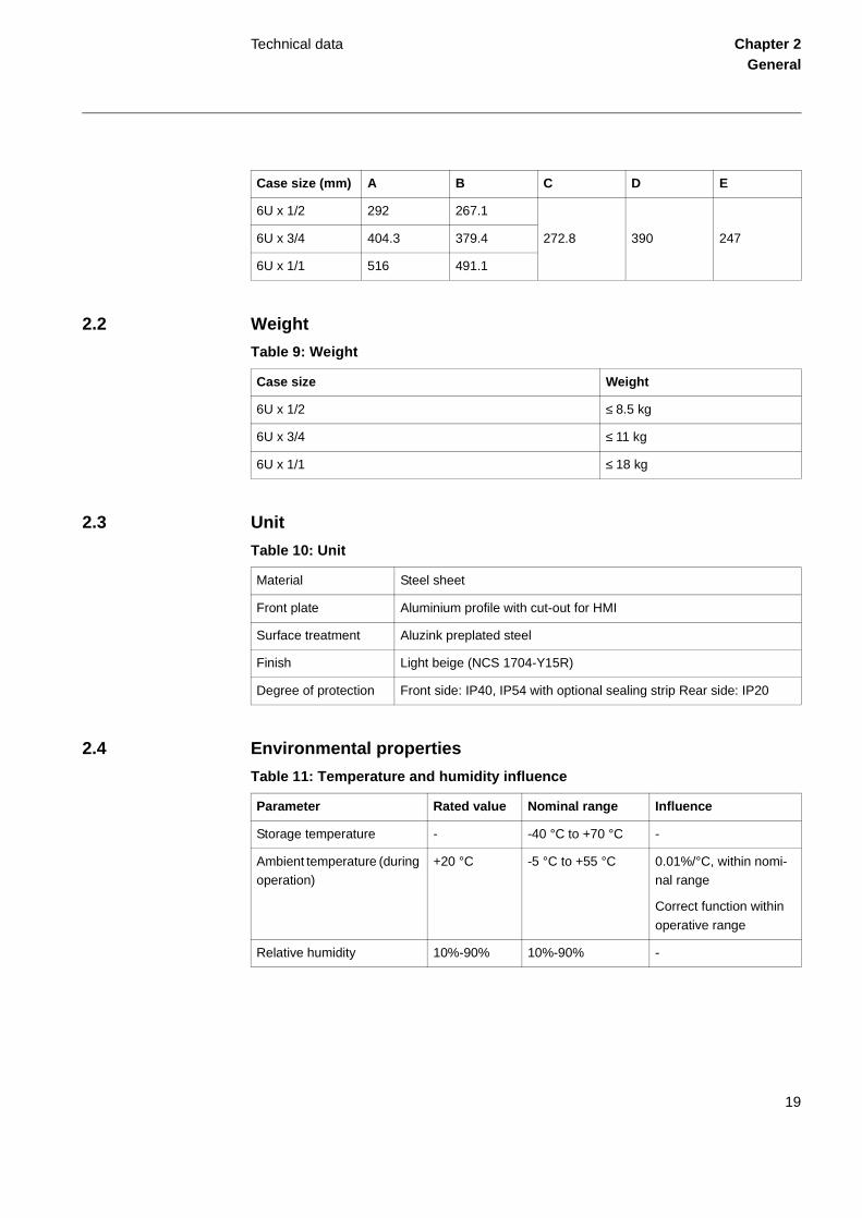
2.2 Weight
Table 9: Weight
2.3 Unit
Table 10: Unit
2.4 Environmental properties
Table 11: Temperature and humidity influence
Case size (mm) A B C D E
6U x 1/2 292 267.1
6U x 3/4 404.3 379.4 272.8 390 247
6U x 1/1 516 491.1
Case size Weight
6U x 1/2 ≤ 8.5 kg
6U x 3/4 ≤ 11 kg
6U x 1/1 ≤ 18 kg
Material Steel sheet
Front plate Aluminium profile with cut-out for HMI
Surface treatment Aluzink preplated steel
Finish Light beige (NCS 1704-Y15R)
Degree of protection Front side: IP40, IP54 with optional sealing strip Rear side: IP20
Parameter Rated value Nominal range Influence
Storage temperature - -40 °C to +70 °C -
Ambient temperature (during operation)
+20 °C -5 °C to +55 °C 0.01%/°C, within nomi-nal range
Correct function within
operative range
Relative humidity 10%-90% 10%-90% -
19
Technical data Chapter 2General
Table 12: Auxiliary DC supply voltage influence on functionality during operation
Table 13: Electromagnetic compatibility
Table 14: Insulation
Table 15: CE compliance
Dependence on: Within nominal range
Within operative range
Ripple, max 12% or EL Negligible Correct function
Interrupted auxiliary
DC voltage
Without reset <50 ms <50 ms
Correct function 0-∞ s 0-∞ s
Restart time <100 s <100 s
Test Type test values Reference standards
1 MHz burst disturbance 2.5 kV IEC 60255-22-1, Class III
Electrostatic discharge 8 kV IEC 60255-22-2, Class III
Fast transient disturbance 4 kV IEC 60255-22-4, Class IV
Radiated electromagnetic field distur-bance
10 V/m, 25-1000 MHz
IEC 60255-22-3, Class III IEEE/ANSI C37.90.2
Test Type test values Reference standard
Dielectric test 2.0 kVAC, 1 min. IEC 60255-5
Impulse voltage test 5 kV, 1.2/50 µs, 0.5 J
Insulation resistance >100 MΩ at 500 VDC
Test According to
Immunity EN 50082-2
Emissivity EN 50081-2
Low voltage directive EN 50178
20
Technical data Chapter 2General
Table 16: Mechanical tests
Test Type test values Reference standards
Vibration Class I IEC 60255-21-1
Shock and bump Class I IEC 60255-21-2
Seismic Class I IEC 60255-21-3
21
Technical data Chapter 2General
22
About this chapter Chapter 3Common functions
Chapter 3 Common functions
About this chapter
This chapter presents the common functions in the terminal.
23
Time synchronisation (TIME) Chapter 3Common functions
1 Time synchronisation (TIME)
1.1 Application
Use the time synchronization source selector to select a common source of absolute time for the terminal when it is a part of a protection system. This makes comparison of events and disturbance data between all terminals in a system possible.
1.2 Function block
1.3 Input and output signals
Table 17: Input signals for the TIME (TIME-) function block
Table 18: Output signals for the TIME (TIME-) function block
xx00000171.vsd
TIME-TIME
MINSYNCSYNCSRC
RTCERRSYNCERR
Signal Description
MINSYNC Minute pulse input
SYNCSRC Synchronization source selector input. See settings for details.
Signal Description
RTCERR Real time clock error
SYNCERR Time synchronisation error
24
Time synchronisation (TIME) Chapter 3Common functions
1.4 Setting parameters
Table 19: Setting parameters for the time synchronization source selector func-tion
Parameter Range Default Unit Description
SYNCSRC 0-5 0 - Selects the time synchronization
source:
0: No source. Internal real time clock is used without fine tuning.
1: LON bus
2: SPA bus
3: IEC 870-5-103 bus
4: Minute pulse, positive flank
5: Minute pulse, negative flank
25
Setting group selector (GRP) Chapter 3Common functions
em the ble
2 Setting group selector (GRP)
2.1 Application
Use the four sets of settings to optimize the terminal’s operation for different systconditions. By creating and switching between fine tuned setting sets, either fromhuman-machine interface or configurable binary inputs, results in a highly adaptaterminal that can cope with a variety of system scenarios.
2.2 Logic diagram
Figure 7: Connection of the function to external circuits
2.3 Function block
GRP--ACTGRP1
GRP--ACTGRP2
GRP--ACTGRP3
GRP--ACTGRP4
IOx-Bly1
IOx-Bly2
IOx-Bly3
IOx-Bly4
+RL2
∅
∅
∅
∅
en01000144.vsd
ACTIVATE GROUP 4ACTIVATE GROUP 3
ACTIVATE GROUP 2
ACTIVATE GROUP 1
xx00000153.vsd
GRP--ACTIVEGROUP
ACTGRP1ACTGRP2ACTGRP3ACTGRP4
GRP1GRP2GRP3GRP4
26
Setting group selector (GRP) Chapter 3Common functions
2.4 Input and output signals
Table 20: Input signals for the ACTIVEGROUP (GRP--) function block
Table 21: Output signals for the ACTIVEGROUP (GRP--) function block
Signal Description
ACTGRP1 Selects setting group 1 as active
ACTGRP2 Selects setting group 2 as active
ACTGRP3 Selects setting group 3 as active
ACTGRP4 Selects setting group 4 as active
Signal Description
GRP1 Setting group 1 is active
GRP2 Setting group 2 is active
GRP3 Setting group 3 is active
GRP4 Setting group 4 is active
27
Setting lockout (HMI) Chapter 3Common functions
3 Setting lockout (HMI)
3.1 Application
Unpermitted or uncoordinated changes by unauthorized personnel may cause severe damage to primary and secondary power circuits. Use the setting lockout function to prevent unauthorized setting changes and to control when setting changes are allowed.
By adding a key switch connected to a binary input a simple setting change control cir-cuit can be built simply allowing only authorized keyholders to make setting changes from the built-in HMI.
3.2 Function block
3.3 Logic diagram
Figure 8: Connection and logic diagram for the BLOCKSET function
xx00000154.vsd
SETTING RESTRICTIONBLOCKSET
SettingRestrict=BlockRESTRICTSETTINGS
HMI--BLOCKSET
&SWITCH
WITH KEY
+
Rex 5xx
en01000152.vsd
28
Setting lockout (HMI) Chapter 3Common functions
3.4 Input and output signals
Table 22: Input signals for the SETTING RESTRICTION function block
3.5 Setting parameters
Table 23: Setting parameters for the setting lockout function
Signal Description
BLOCKSET Input signal to block setting and/or configuration changes
from the local HMI. WARNING: Read the instructions before use. Default configuration to NONE-NOSIGNAL.
Parameter Range Default Unit Description
SettingRestrict Open, Block
Open - Open: Setting parameters can be changed.
Block: Setting parameters can only
be changed if the logic state of the BLOCKSET input is zero.
29
I/O system configurator (IOP) Chapter 3Common functions
cog-nd pro-
4 I/O system configurator (IOP)
4.1 Application
The I/O system configurator must be used in order for the terminal’s software to renize added modules and to create internal address mappings between modules atections and other functions.
4.2 Logic diagram
Figure 9: Example of an I/O-configuration in the graphical tool CAP 531 for a REx 5xx with two BIMs.
IOP1-
S11
S14S15S16S17S18
S13S12
S19S20S21
S23S22
I/OPosition
S24S25S26S27S28S30S32S34S36
IO01-
IO02-
I/O-module
I/O-module
POSITION ERRORBI1
BI6
.
.
.
POSITION ERROR
BI1
BI6
.
.
.
en01000143.vsd
30
I/O system configurator (IOP) Chapter 3Common functions
4.3 Function block
4.4 Input and output signals
Table 24: Output signals for the I/OPOSITION (IOPn-) function block
I/O nodes = BIM, BOM, IOM PSM, MIM or DCMDSP = Digital Signal Processorxxxx = Inverted signal
99000034.vsd
33
Self supervision (INT) Chapter 3Common functions
Figure 11: Software self-supervision, function block INTernal signals
Checksum
Node reports
Synch error
NO RX Data
NO TX Clock
Check RemError
&
>1
>1
INT--ADC
Send Rem Error
OK
OK
>1TIME-RTCERR INT--CPUWARN
>1
TIME-SYNCERRRTC-WARNINGINT--CPUWARN
INT--WARNING
Watchdog
Check CRC
RAM check
DSP Modules, 1-12
OK
OK
OK&
OKINT--CPUFAIL
Parameter check
Watchdog
Flow control
&
OK
OK
OK&
>1
INT--CPUFAILINT--ADC
I/O node FAILINT--FAIL
Start-up self-test Fault
MainCPU
Remoteterminalcommunication
A/D ConverterModule
RTC-WARNING = DIFL-COMFAIL or RTC1-COMFAIL + RTC2-COMFAIL
I/O node = BIM, BOM, IOM, PSM, MIM, DCM (described in the hardware design)
99000035.vsd
>1
RTC-WARNING
34
Self supervision (INT) Chapter 3Common functions
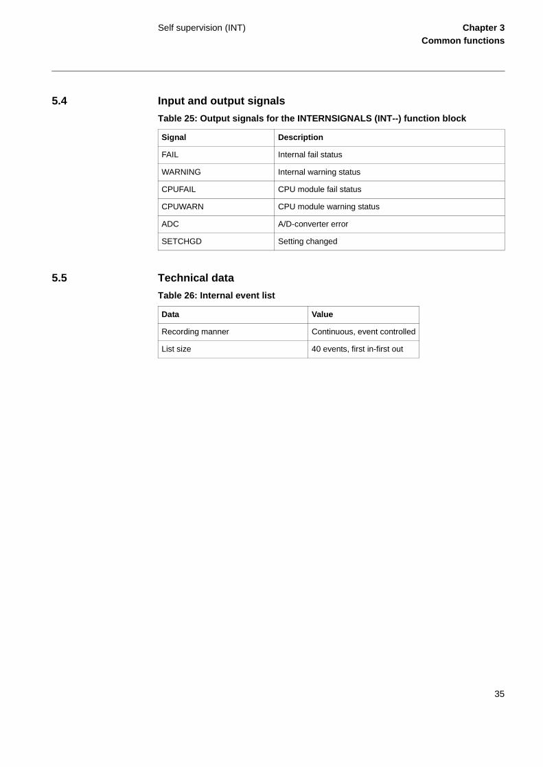
5.4 Input and output signals
Table 25: Output signals for the INTERNSIGNALS (INT--) function block
5.5 Technical data
Table 26: Internal event list
Signal Description
FAIL Internal fail status
WARNING Internal warning status
CPUFAIL CPU module fail status
CPUWARN CPU module warning status
ADC A/D-converter error
SETCHGD Setting changed
Data Value
Recording manner Continuous, event controlled
List size 40 events, first in-first out
35
Logic function blocks Chapter 3Common functions
6 Logic function blocks
6.1 Application
The user can with the available logic function blocks build logic functions and config-ure the terminal to meet application specific requirements.
Different protection, control, and monitoring functions within the REx 5xx terminals are quite independent as far as their configuration in the terminal is concerned. The user can not change the basic algorithms for different functions. But these functions com-bined with the logic function blocks can be used to create application specific function-ality.
With additional configurable logic means that an extended number of logic circuits are available. Also Move function blocks (MOF, MOL), used for synchronization of bool-ean signals sent between logics with slow and fast execution, are among the additional configurable logic circuits.
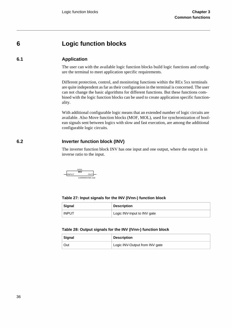
6.2 Inverter function block (INV)
The inverter function block INV has one input and one output, where the output is in inverse ratio to the input.
Table 27: Input signals for the INV (IVnn-) function block
Table 28: Output signals for the INV (IVnn-) function block
Signal Description
INPUT Logic INV-Input to INV gate
Signal Description
Out Logic INV-Output from INV gate
xx00000158.vsd
IV01-INV
INPUT OUT
36
Logic function blocks Chapter 3Common functions
6.3 OR function block (OR)
The OR function is used to form general combinatory expressions with boolean vari-ables. The OR function block has six inputs and two outputs. One of the outputs is in-verted.
Table 29: Input signals for the OR (Onnn-) function block
Table 30: Output signals for the OR (Onnn-) function block
6.4 AND function block (AND)
The AND function is used to form general combinatory expressions with boolean vari-ables.The AND function block has four inputs and two outputs. One of the inputs and one of the outputs are inverted.
Signal Description
INPUT1 Input 1 to OR gate
INPUT2 Input 2 to OR gate
INPUT3 Input 3 to OR gate
INPUT4 Input 4 to OR gate
INPUT5 Input 5 to OR gate
INPUT6 Input 6 to OR gate
Signal Description
OUT Output from OR gate
NOUT Inverted output from OR gate
xx00000159.vsd
O001-OR
INPUT1INPUT2INPUT3INPUT4INPUT5INPUT6
OUTNOUT
37
Logic function blocks Chapter 3Common functions
Table 31: Input signals for the AND (Annn-) function block
Table 32: Output signals for the AND (Annn-) function block
6.5 Timer function block (TM)
The function block TM timer has drop-out and pick-up delayed outputs related to the input signal. The timer has a settable time delay (parameter T) between 0.000 and 60.000 s in steps of 0.001 s.
Table 33: Input signals for the TIMER (TMnn-) function block
Signal Description
INPUT1 Input 1 to AND gate
INPUT2 Input 2 to AND gate
INPUT3 Input 3 to AND gate
INPUT4N Input 4 (inverted) to AND gate
Signal Description
OUT Output from AND gate
NOUT Inverted output from AND gate
xx00000160.vsd
A001-AND
INPUT1INPUT2INPUT3INPUT4N
OUTNOUT
Signal Description
INPUT Input to timer
T Time value. See setting parameters
xx00000161.vsd
TM01-TIMER
INPUTT
OFFON
38
Logic function blocks Chapter 3Common functions
Table 34: Output signals for the TIMER (TMnn-) function block
6.5.1 Setting parameters
Table 35: Setting parameters for the Timer (TMnn-) function
6.6 Timer long function block (TL)
The function block TL timer with extended maximum time delay at pick-up and at drop-out, is identical with the TM timer. The difference is the longer time delay, settable be-tween 0.0 and 90000.0 s in steps of 0.1 s
Table 36: Input signals for the TIMERLONG (TLnn-) function block
Table 37: Output signals for the TIMERLONG (TLnn-) function block
Signal Description
OFF Output from timer, drop-out delayed
ON Output from timer , pick-up delayed
Parameter Range Default Unit Description
T 0.000-60.000
Step: 0.001
0.000 s Delay for timer nn
Signal Description
INPUT Input to long timer
T Time value. See setting parameters
Signal Description
OFF Output from long timer, drop-out delayed
ON Output from long timer, pick-up delayed
xx00000162.vsd
TL01-TIMERLONG
INPUTT
OFFON
39
Logic function blocks Chapter 3Common functions
6.6.1 Setting parameters
Table 38: Setting parameters for the TimerLong (TLnn-) function
6.7 Pulse timer function block (TP)
The pulse function can be used, for example, for pulse extensions or limiting of opera-tion of outputs. The pulse timer TP has a settable length of a pulse between 0.000 s and 60.000 s in steps of 0.010 s.
Table 39: Input signals for the TP (TPnn-) function block
Table 40: Output signals for the TP (TPnn-) function block
6.7.1 Setting parameters
Table 41: Setting parameters for the Pulse (TPnn-) function
Parameter Range Default Unit Description
T 0.0-90000.0
Step:0.1
0.0 s Delay for TLnn function
Signal Description
INPUT Input to pulse timer
T Pulse length. See setting parameters
Signal Description
OUT Output from pulse timer
xx00000163.vsd
TP01-PULSE
INPUTT
OUT
Parameter Range Default Unit Description
T 0.000-
60.000
Step:0.010
0.010 s Pulse length
40
Logic function blocks Chapter 3Common functions
6.8 Extended length pulse function block (TQ)
The function block TQ pulse timer with extended maximum pulse length, is identical with the TP pulse timer. The difference is the longer pulse length, settable between 0.0 and 90000.0 s in steps of 0.1 s.
Table 42: Input signals for the PULSELONG (TQnn-) function block
Table 43: Output signals for the PULSELONG (TQnn-) function block
6.8.1 Setting parameters
Table 44: Setting parameters for the PulseLong (TQnn-) function
6.9 Exclusive OR function block (XO)
The exclusive OR function XOR is used to generate combinatory expressions with boolean variables. The function block XOR has two inputs and two outputs. One of the outputs is inverted. The output signal is 1 if the input signals are different and 0 if they are equal.
Signal Description
INPUT Input to pulse long timer
T Pulse length. See setting parameters
Signal Description
OUT Output from pulse long timer
xx00000164.vsd
TQ01-PULSELONG
INPUTT
OUT
Parameter Range Default Unit Description
T 0.0-90000.0
Step: 0.1
0.0 s Pulse length
xx00000165.vsd
XO01-XOR
INPUT1INPUT2
OUTNOUT
41
Logic function blocks Chapter 3Common functions
Table 45: Input signals for the XOR (XOnn-) function block
Table 46: Output signals for the XOR (XOnn-) function block
6.10 Set-reset function block (SR)
The Set-Reset (SR) function is a flip-flop that can set or reset an output from two inputs respectively. Each SR function block has two outputs, where one is inverted.
Table 47: Input signals for the SR (SRnn-) function block
Table 48: Output signals for the SR (SRnn-) function block
Signal Description
INPUT1 Input 1 to XOR gate
INPUT2 Input 2 to XOR gate
Signal Description
OUT Output from XOR gate
NOUT Inverted output from XOR gate
Signal Description
SET Input to SR flip-flop
RESET Input to SR flip-flop
Signal Description
OUT Output from SR flip-flop
NOUT Inverted output from SR flip-flop
xx00000166.vsd
SR01-SR
SETRESET
OUTNOUT
42
Logic function blocks Chapter 3Common functions
6.11 Set-reset with memory function block (SM)
The Set-Reset function SM is a flip-flop with memory that can set or reset an output from two inputs respectively. Each SM function block has two outputs, where one is inverted. The memory setting controls if the flip-flop after a power interruption will re-turn the state it had before or if it will be reset.
Table 49: Input signals for the SRM (SMnn-) function block
Table 50: Output signals for the SRM (SMnn-) function block
Table 51: Setting parameters for the SRM (SMnn-) function
6.12 Controllable gate function block (GT)
The GT function block is used for controlling if a signal should be able to pass from the input to the output or not depending on a setting.
Signal Description
SET Input to SRM flip-flop
RESET Input to SRM flip-flop
Signal Description
OUT Output from SRM flip-flop
NOUT Inverted output from SRM flip-flop
Parameter Range Default Unit Description
Memory Off/On Off - Operating mode of the memory function
xx00000382.vsd
SM01-SRM
SETRESET
OUTNOUT
xx00000380.vsd
GT01-GT
INPUT OUT
43
Logic function blocks Chapter 3Common functions
Table 52: Input signals for the GT (GTnn-) function block
Table 53: Output signals for the GT (GTnn-) function block
6.12.1 Setting parameters
Table 54: Setting parameters for the GT (GTnn-) function
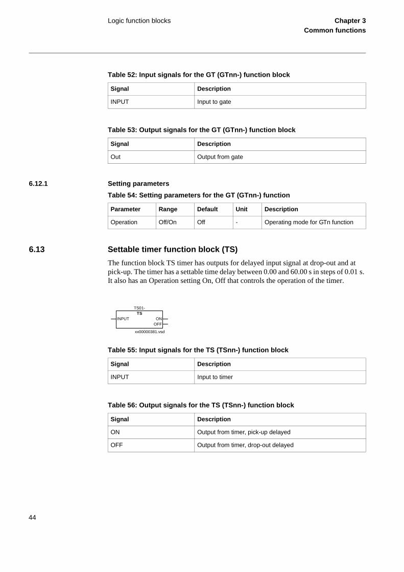
6.13 Settable timer function block (TS)
The function block TS timer has outputs for delayed input signal at drop-out and at pick-up. The timer has a settable time delay between 0.00 and 60.00 s in steps of 0.01 s. It also has an Operation setting On, Off that controls the operation of the timer.
Table 55: Input signals for the TS (TSnn-) function block
Table 56: Output signals for the TS (TSnn-) function block
Signal Description
INPUT Input to gate
Signal Description
Out Output from gate
Parameter Range Default Unit Description
Operation Off/On Off - Operating mode for GTn function
Signal Description
INPUT Input to timer
Signal Description
ON Output from timer, pick-up delayed
OFF Output from timer, drop-out delayed
xx00000381.vsd
TS01-TS
INPUT ONOFF
44
Logic function blocks Chapter 3Common functions
6.13.1 Setting parameters
Table 57: Setting parameters for the TS (TSn-) function
6.14 Move first function block (MOF)
The Move function block MOF is put First in the slow logic and is used for signals com-ing from fast logic into the slow logic. The MOF function block is only a temporary storage for the signals and do not change any value between input and output.
6.14.1 Function block
Table 58: Input signals for the MOFx function block
Table 59: Output signals for the MOFx function block
Parameter Range Default Unit Description
Operation Off/On Off - Operating mode for TSn function
The Move function block MOL is put Last in the slow logic and is used for signals go-ing out from the slow logic to the fast logic. The MOL function block is only a tempo-rary storage for the signals and do not change any value between input and output.
Table 60: Input signals for the MOLx function block
Table 61: Output signals for the MOLx function block
Blocking of signals during test Chapter 3Common functions
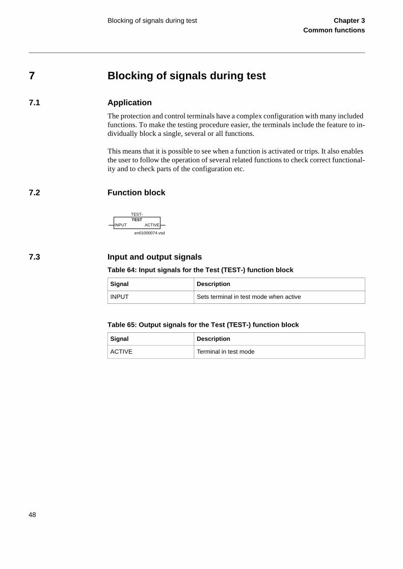
7 Blocking of signals during test
7.1 Application
The protection and control terminals have a complex configuration with many included functions. To make the testing procedure easier, the terminals include the feature to in-dividually block a single, several or all functions.
This means that it is possible to see when a function is activated or trips. It also enables the user to follow the operation of several related functions to check correct functional-ity and to check parts of the configuration etc.
7.2 Function block
7.3 Input and output signals
Table 64: Input signals for the Test (TEST-) function block
Table 65: Output signals for the Test (TEST-) function block
TEST-TEST
INPUT ACTIVE
en01000074.vsd
Signal Description
INPUT Sets terminal in test mode when active
Signal Description
ACTIVE Terminal in test mode
48
About this chapter Chapter 4Line impedance
Chapter 4 Line impedance
About this chapter
This chapter describes the line impedance functions in the terminal.
49
Pole slip protection (PSP) Chapter 4Line impedance
1 Pole slip protection (PSP)
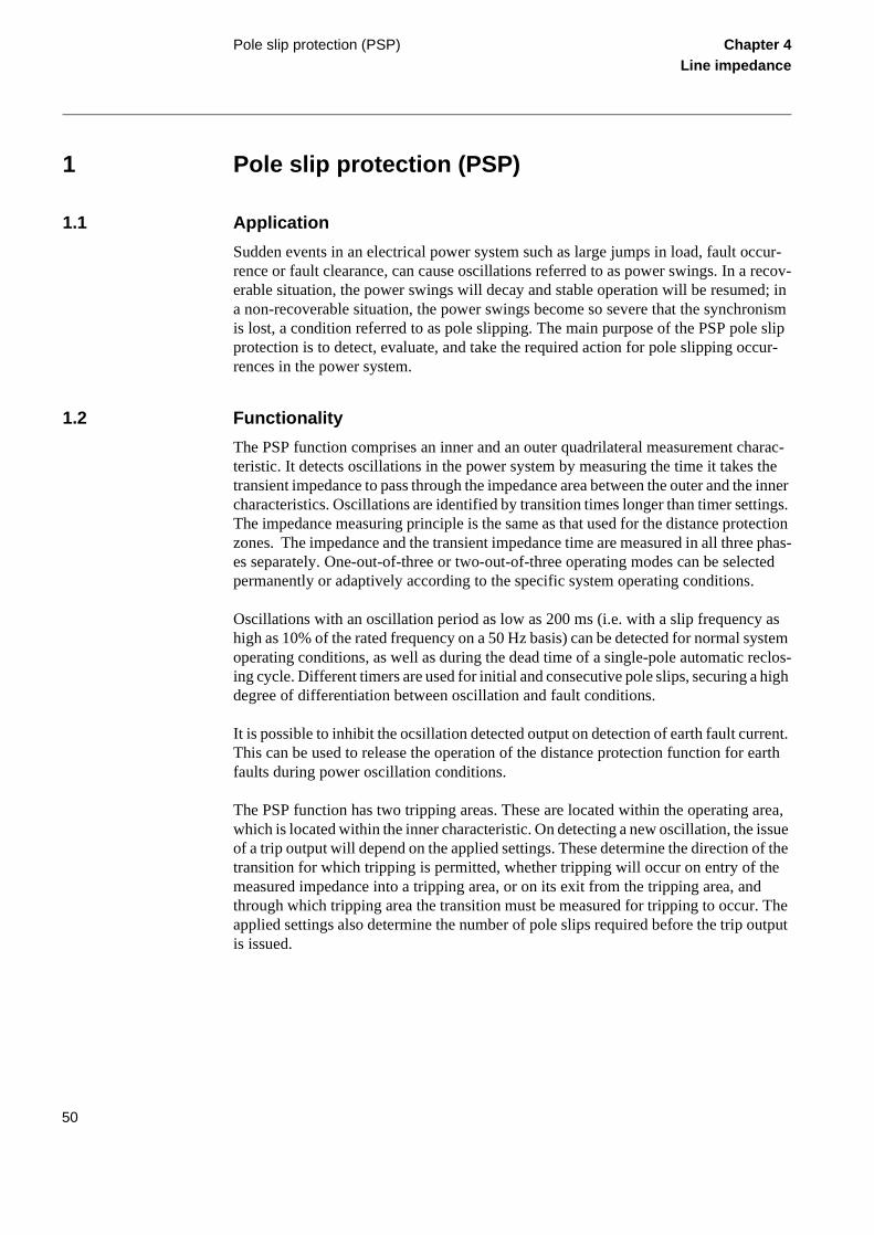
1.1 Application
Sudden events in an electrical power system such as large jumps in load, fault occur-rence or fault clearance, can cause oscillations referred to as power swings. In a recov-erable situation, the power swings will decay and stable operation will be resumed; in a non-recoverable situation, the power swings become so severe that the synchronism is lost, a condition referred to as pole slipping. The main purpose of the PSP pole slip protection is to detect, evaluate, and take the required action for pole slipping occur-rences in the power system.
1.2 Functionality
The PSP function comprises an inner and an outer quadrilateral measurement charac-teristic. It detects oscillations in the power system by measuring the time it takes the transient impedance to pass through the impedance area between the outer and the inner characteristics. Oscillations are identified by transition times longer than timer settings. The impedance measuring principle is the same as that used for the distance protection zones. The impedance and the transient impedance time are measured in all three phas-es separately. One-out-of-three or two-out-of-three operating modes can be selected permanently or adaptively according to the specific system operating conditions.
Oscillations with an oscillation period as low as 200 ms (i.e. with a slip frequency as high as 10% of the rated frequency on a 50 Hz basis) can be detected for normal system operating conditions, as well as during the dead time of a single-pole automatic reclos-ing cycle. Different timers are used for initial and consecutive pole slips, securing a high degree of differentiation between oscillation and fault conditions.
It is possible to inhibit the ocsillation detected output on detection of earth fault current. This can be used to release the operation of the distance protection function for earth faults during power oscillation conditions.
The PSP function has two tripping areas. These are located within the operating area, which is located within the inner characteristic. On detecting a new oscillation, the issue of a trip output will depend on the applied settings. These determine the direction of the transition for which tripping is permitted, whether tripping will occur on entry of the measured impedance into a tripping area, or on its exit from the tripping area, and through which tripping area the transition must be measured for tripping to occur. The applied settings also determine the number of pole slips required before the trip output is issued.
50
Pole slip protection (PSP) Chapter 4Line impedance
1.3 Function block
1.4 Logic diagram
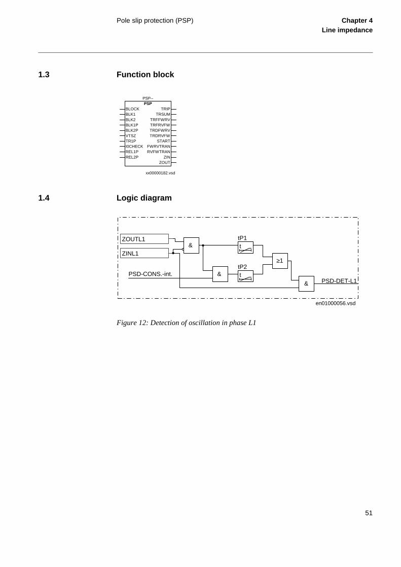
Figure 12: Detection of oscillation in phase L1
xx00000182.vsd
PSP--PSP
BLOCKBLK1BLK2BLK1PBLK2PVTSZTR1PI0CHECKREL1PREL2P
TRIPTRSUM
TRFFWRVTRFRVFWTRDFWRVTRDRVFW
STARTFWRVTRANRVFWTRAN
ZINZOUT
en01000056.vsd
ZOUTL1&
ZINL1ttP1
ttP2
&PSD-DET-L1
PSD-CONS.-int.
≥1
&
51
Pole slip protection (PSP) Chapter 4Line impedance
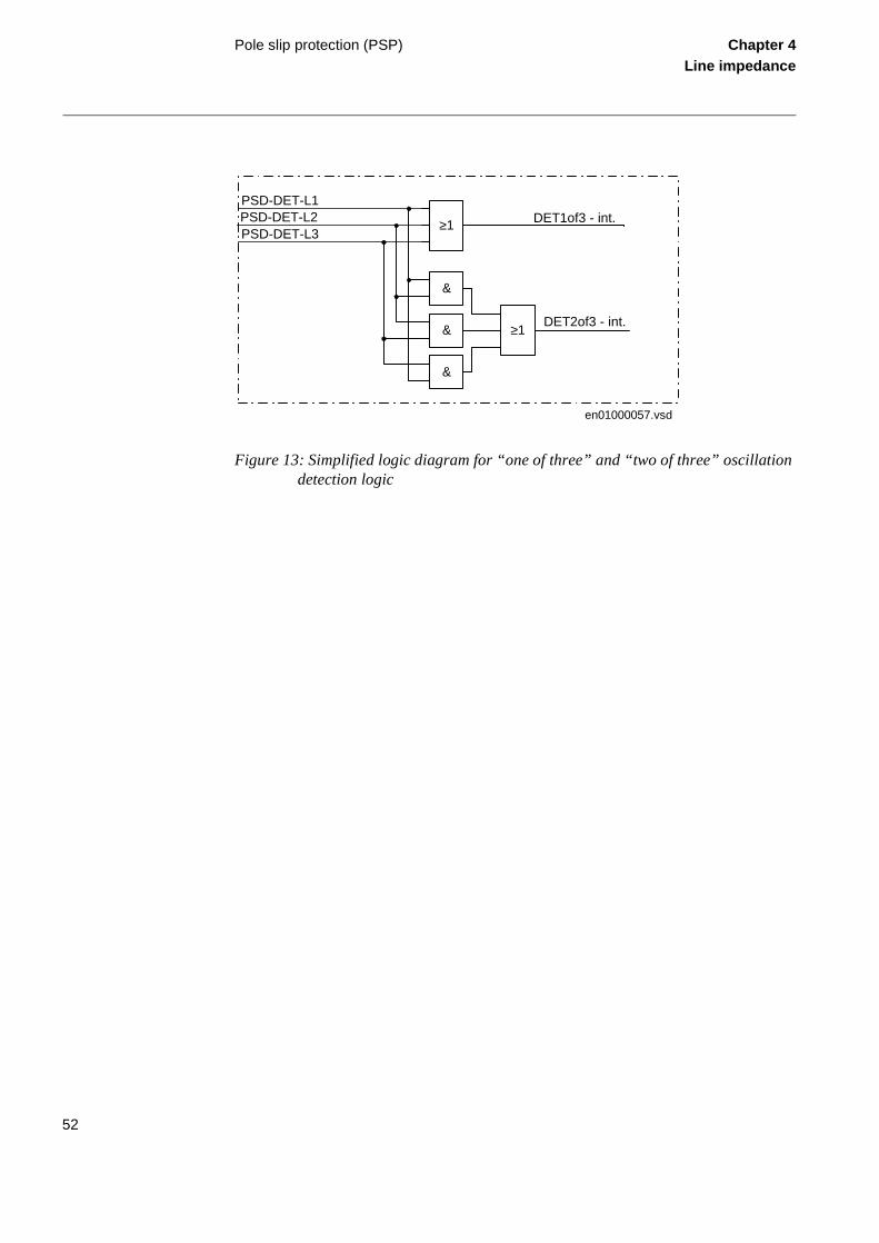
Figure 13: Simplified logic diagram for “one of three” and “two of three” oscillationdetection logic
en01000057.vsd
PSD-DET-L1PSD-DET-L2PSD-DET-L3
DET1of3 - int.
DET2of3 - int.
&
&
&
≥1
≥1
52
Pole slip protection (PSP) Chapter 4Line impedance
Figure 14: Simplified logic diagram for cooperation with distance protection function
PSP--TRSPt
tEF&
PSP--I0CHECK
&DET-int.
PSP--BLK2
&
t10 ms
>1
ttR1
>1
&PSP--BLK1 ttR2
PSP--BLOCK
ZOUTPSL3
ZOUTPSL2
ZOUTPSL1
&
DET1of3 - int.
PSP--REL1P
PSP--BLK1P&
DET2of3 - int.
PSP--REL2P
PSP--BLK2P&
>1 ttHZ PSP--START
>1PSP--ZOUT
ZINPSL1
ZINPSL2
ZINPSL3
>1PSP--ZIN
99001032.vsd
INHIBIT
&
53
Pole slip protection (PSP) Chapter 4Line impedance
Figure 15: The impedance operating plane is divided in two detection regions and two trip regions.
1 Forward - reverse detection region
2 Reverse - forward detection region
3 Fast trip region
4 Delayed trip region
5 System impedance
6 Internal operating boundary
7 External operating boundary
jX
RR1RTRR1LTR
SCA
en01000062.vsd
5
2
1
4
3
6
7
54
Pole slip protection (PSP) Chapter 4Line impedance
Figure 16: Flow-chart presenting the operation of the pole slip protection for the for-ward to reverse transition (FwRv) after the oscillation has been detected.
en00000717.vsd
New FwRvoscillation detected
TRFwRv=On
TRFastFwRv=On
Impedancewithin fast
region
TRIncFwRv=On
Impedance passesR1RTR
TRIP
START
TRDelFwRv=On
Impedancewithin delay
region
TRIncFwRv=On
Impedance passesR1RTR
TROutFwRv=On
Impedance passesR1LTR
TROutFwRv=On
Impedance passesR1LTR
nFast=nFastFwRv nDel=nDelFwRvOscillation
FwRvCompleted
nDel=nDel+1Oscillation
FwRvCompleted
nFast=nFast+1
Next FwRv oscillationdetected before tW
elapsed
Next FwRv oscillationdetected before tW
elapsed
YESNONO
YES
YES
YES
YES YES
YES
YES YES
YESYES YES YES
NO
NO NO
NONO
NO NO YESYES
NONO NONO
NONO
YESYES YES YES
NONO
YES YES
55
Pole slip protection (PSP) Chapter 4Line impedance
Figure 17: Flow-chart presenting the operation of the pole slip protection for the re-verse to forward transition (RvFw) after the oscillation has been detected.
en00000718.vsd
New RvFwoscillation detected
TRRvFw
TRFastRvFw=On
Impedancewithin fast
region
TRIncRvFw=On
Impedance passesR1LTR
TRIP
START
TRDelRvFw=On
Impedancewithin delay
region
TRIncRvFw=On
Impedance passesR1LTR
TROutRvFw=On
Impedance passesR1RTR
TROutRvFw=On
Impedance passesR1RTR
nFast=nFastRvFw nDel=nDelRvFwOscillation
RvFwCompleted
nDel=nDel+1Oscillation
RvFwCompleted
nFast=nFast+1
Next RvFw oscillationdetected before tW
elapsed
Next RvFw oscillationdetected before tW
elapsed
YESNONO
YES
YES
YES
YES YES
YES
YES YES
YESYES YES YES
NO
NO NO
NONO
NO NO YESYES
NONO NONO
NONO
YESYES YES YES
NONO
YES YES
=On
56
Pole slip protection (PSP) Chapter 4Line impedance
Figure 18: Flow-chart presenting summation trip (TRIPSUM) of the pole slip protec-tion for the forward to reverse transition (FwRv).
New FwRv oscillationdetected
TRFwRv=On
TRFastFwRv=On
Impedancewithin fast
region
TRIncFwRv=On
Impedance passesR1RTR
TRIPSUM
START
TRDelFwRv=On
Impedancewithin delay
region
TROutFwRv=On
Impedance passesR1LTR
nSum=nDelFwRvOscillation
FwRvCompeited
nSum=nSum+1
Next FwRv oscillationdetected before tW
elapsed
YESNO
YES
YES
YES
YES YES
YES
YES
YESYES
NO
NO NO
NONO
NOYES
NONO
NO
YES YES
NO
YES
en00000719.vsd
57
Pole slip protection (PSP) Chapter 4Line impedance
Figure 19: Flow-chart presenting summation trip (TRIPSUM) of the pole slip protec-tion for the reverse to forward transition (RvFw).
New RvFw oscillationdetected
TRRvFw=On
TRFastRvFw=On
Impedancewithin fast
region
TRIncRvFw=On
Impedance passesR1LTR
TRIPSUM
START
TRDelRvFw=On
Impedancewithin delay
region
TROutRvFw=On
Impedance passesR1RTR
nSum=nDelRvFwOscillation
RvFwCompleted
nSum=nSum+1
Next RvFw oscillationdetected before tW
elapsed
YESNO
YES
YES
YES
YES YES
YES
YES
YESYES
NO
NO NO
NONO
NOYES
NONO
NO
YES YES
NO
YES
en00000720.vsd
58
Pole slip protection (PSP) Chapter 4Line impedance
1.5 Input and output signals
Table 66: Input signals for the PSP (PSP--) function block
Table 67: Output signals for the PSP (PSP--) function block
Signal Description
BLOCK Blocks function
BLK1 Blocks the inhibit condition controlled by the tR2 timer
BLK2 Blocks the inhibit condition based on residual current detec-tion, unless within tEF timer following 1-pole trip
BLK1P Blocks one-out-of-three phase detection of the oscillation
BLK2P Blocks two-out-of-three phase detection of the oscillation
VTSZ Blocks the operation of the PSP on fuse failure detection
TR1P Starts the tEF timer for 1-pole trip
I0CHECK Residual current detection used to inhibit PSP-START output
REL1P Releases one-out-of-three phase detection of the oscillation
REL2P Releases two-out-of-three phase detection of the oscillation
Signal Description
TRIP Trip output
TRSUM Delayed trip caused by transitions passing either delayed or fast tripping area
TRFFWRV Fast trip for forward to reverse transition
TRFRVFW Fast trip for reverse to forward transition
TRDFWRV Delayed trip for forward to reverse transition
TRDRVFW Delayed trip for reverse to forward transition
START Oscillation detected
FWRVTRAN Forward to reverse direction transition detected
RVFWTRAN Reverse to forward direction transition detected
ZIN Measured impedance within the inner characteristic boundary
ZOUT Measured impedance within the outer characteristic boundary
59
Pole slip protection (PSP) Chapter 4Line impedance
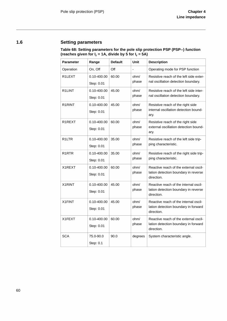
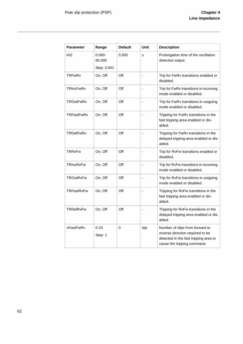
1.6 Setting parameters
Table 68: Setting parameters for the pole slip protection PSP (PSP--) function (reaches given for Ir = 1A, divide by 5 for Ir = 5A)
Parameter Range Default Unit Description
Operation On, Off Off - Operating mode for PSP function
R1LEXT 0.10-400.00
Step: 0.01
60.00 ohm/phase
Resistive reach of the left side exter-nal oscillation detection boundary.
R1LINT 0.10-400.00
Step: 0.01
45.00 ohm/phase
Resistive reach of the left side inter-nal oscillation detection boundary.
R1RINT 0.10-400.00
Step: 0.01
45.00 ohm/
phase
Resistive reach of the right side
internal oscillation detection bound-ary.
R1REXT 0.10-400.00
Step: 0.01
60.00 ohm/
phase
Resistive reach of the right side
external oscillation detection bound-ary.
R1LTR 0.10-400.00
Step: 0.01
35.00 ohm/
phase
Resistive reach of the left side trip-
ping characteristic.
R1RTR 0.10-400.00
Step: 0.01
35.00 ohm/phase
Resistive reach of the right side trip-ping characteristic.
X1REXT 0.10-400.00
Step: 0.01
60.00 ohm/phase
Reactive reach of the external oscil-lation detection boundary in reverse
direction.
X1RINT 0.10-400.00
Step: 0.01
45.00 ohm/phase
Reactive reach of the internal oscil-lation detection boundary in reverse
direction.
X1FINT 0.10-400.00
Step: 0.01
45.00 ohm/phase
Reactive reach of the internal oscil-lation detection boundary in forward
direction.
X1FEXT 0.10-400.00
Step: 0.01
60.00 ohm/phase
Reactive reach of the external oscil-lation detection boundary in forward
direction.
SCA 75.0-90.0
Step: 0.1
90.0 degrees System characteristic angle.
60
Pole slip protection (PSP) Chapter 4Line impedance
X1PSLFw 0.10-400.00
Step: 0.01
35.00 ohm/
phase
Positive sequence reactance deter-
mining the forward reactive reach of the fast tripping zone.
R1PSLFw 0.10-400.00
Step: 0.01
1.50 ohm/phase
Positive sequence resistance deter-mining the forward resistive reach of the fast tripping zone.
X1PSLRv 0.10-400.00
Step: 0.01
0.10 ohm/phase
Positive sequence reactance deter-mining the reverse reactive reach of the fast tripping zone.
R1PSLRv 0.10-400.00
Step: 0.01
0.10 ohm/phase
Positive sequence resistance deter-mining the reverse resistive reach of the fast tripping zone.
tP1 0.000-60.000
Step: 0.001
0.045 s Transition time used for the detec-tion of the initial oscillation
tP2 0.000-
60.000
Step: 0.001
0.015 s Transition time used for the detec-
tion of subsequent oscillations.
tW 0.000-60.000
Step: 0.001
0.350 s Waiting time to distinguish between new and subsequent oscillations.
tEF 0.000-60.000
Step: 0.001
3.000 s Time window after single pole trip-ping in which to allow residual cur-rent detection to inhibit the output for
a detected oscillation.
tR1 0.000-60.000
Step: 0.001
0.040 s Time delay required to inhibit the oscillation detected output by resid-
ual current detection following oscil-lation detection.
tR2 0.000-
60.000
Step: 0.001
2.000 s Time delay required for the mea-
sured impedance to remain within the oscillation detection area before inhibiting the oscillation detected
output.
Parameter Range Default Unit Description
61
Pole slip protection (PSP) Chapter 4Line impedance
tHZ 0.000-
60.000
Step: 0.001
0.500 s Prolongation time of the oscillation
detected output.
TRFwRv On, Off Off - Trip for FwRv transitions enabled or
disabled.
TRIncFwRv On, Off Off - Trip for FwRv transitions in incoming mode enabled or disabled.
TROutFwRv On, Off Off - Trip for FwRv transitions in outgoing mode enabled or disabled.
TRFastFwRv On, Off Off - Tripping for FwRv transitions in the
fast tripping area enabled or dis-abled.
TRDelFwRv On, Off Off - Tripping for FwRv transitions in the
delayed tripping area enabled or dis-abled.
TRRvFw On, Off Off - Trip for RvFw transitions enabled or
disabled.
TRIncRvFw On, Off Off - Trip for RvFw transitions in incoming mode enabled or disabled.
TROutRvFw On, Off Off - Trip for RvFw transitions in outgoing mode enabled or disabled.
TRFastRvFw On, Off Off - Tripping for RvFw transitions in the
fast tripping area enabled or dis-abled.
TRDelRvFw On, Off Off - Tripping for RvFw transitions in the
delayed tripping area enabled or dis-abled.
nFastFwRv 0-10
Step: 1
0 slip Number of slips from forward to
reverse direction required to be detected in the fast tripping area to cause the tripping command.
Parameter Range Default Unit Description
62
Pole slip protection (PSP) Chapter 4Line impedance
1.7 Technical data
Table 69: Pole slip protection
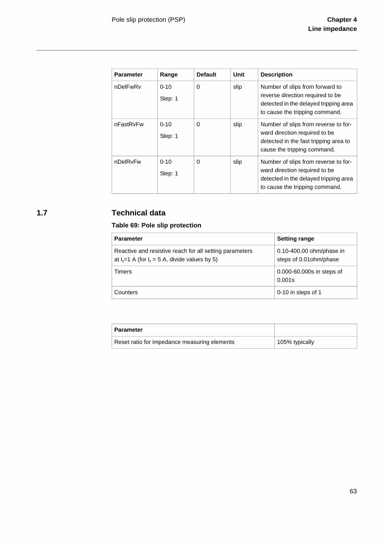
nDelFwRv 0-10
Step: 1
0 slip Number of slips from forward to
reverse direction required to be detected in the delayed tripping area
to cause the tripping command.
nFastRvFw 0-10
Step: 1
0 slip Number of slips from reverse to for-ward direction required to be
detected in the fast tripping area to cause the tripping command.
nDelRvFw 0-10
Step: 1
0 slip Number of slips from reverse to for-
ward direction required to be detected in the delayed tripping area to cause the tripping command.
Parameter Range Default Unit Description
Parameter Setting range
Reactive and resistive reach for all setting parameters
at Ir=1 A (for Ir = 5 A, divide values by 5)
0.10-400.00 ohm/phase in
steps of 0.01ohm/phase
Timers 0.000-60.000s in steps of 0.001s
Counters 0-10 in steps of 1
Parameter
Reset ratio for impedance measuring elements 105% typically
63
Pole slip protection (PSP) Chapter 4Line impedance
64
About this chapter Chapter 5Current
Chapter 5 Current
About this chapter
This chapter describes the current protection functions
65
Instantaneous overcurrent protection (IOC)
Chapter 5Current
ion or unc-
ases nces
above ip sig-nc-
com-d dc e the
trip tion.
1 Instantaneous overcurrent protection (IOC)
1.1 Application
Different system conditions, such as source impedance and the position of the faults on long transmission lines influence the fault currents to a great extent. An instantaneous phase overcurrent protection with short operate time and low transient overreach of the measuring elements can be used to clear close-in faults on long power lines, where short fault clearing time is extremely important to maintain system stability.
The instantaneous residual overcurrent protection can be used in a number of applica-tions. Below some examples of applications are given.
• Fast back-up earth fault protection for faults close to the line end.
• Enables fast fault clearance for close in earth faults even if the distance protectthe directional residual current protection is blocked from the fuse supervision ftion
1.2 Functionality
The current measuring element continuously measures the current in all three phand compares it to the set operate value IP>>. A filter ensures immunity to disturbaand dc components and minimizes the transient overreach. If any phase current isthe set value IP>>, the phase overcurrent trip signal TRP is activated. Separate trnal for the actual phase(s) is also activated. The input signal BLOCK blocks all futions in the current function block.
The current measuring element continuously measures the residual current and pares it to the set operate value IN>>. A filter ensures immunity to disturbances ancomponents and minimizes the transient overreach. If the residual current is abovset value IN>>, the residual overcurrent trip signal TRN is activated. The generalsignal TRIP is activated as well. The input signal BLOCK blocks the complete func
66
Instantaneous overcurrent protection (IOC)
Chapter 5Current
1.3 Function block
Figure 20: IOC function block phase + N with 1, 2, 3 phase trip
Figure 21: IOC function block, phase + N with 3 phase trip
Figure 22: IOC function block phase with 1, 2, 3 phase trip
Figure 23: IOC function block, phase with 3 phase trip
xx00000201.vsd
IOC--IOC
BLOCK TRIPTRP
TRL1TRL2TRL3TRN
xx01000176.vsd
IOC--IOC
BLOCK TRIPTRPTRN
xx00000683.vsd
IOC--IOC
BLOCK TRIPTRP
TRL1TRL2TRL3
xx01000079.vsd
IOC--IOC
BLOCK TRIPTRP
67
Instantaneous overcurrent protection (IOC)
Chapter 5Current
Figure 24: IOC function block, N + 3 phase trip
1.4 Logic diagram
Figure 25: IOC function, logic diagram
xx00000684.vsd
IOC--IOC
BLOCK TRIPTRN
IOC--BLOCK
IOC--TRIP
en01000180.vsd
&
Function Enable
IOC - INSTANTANEOUS PHASE OVERCURRENT FUNCTION
>1
STIL1
&
&
&
&
STIL2
STIL3
IOC--TRP
IOC--TRL1
IOC--TRL2
IOC--TRL3
>1>1
&IOC--TRN
STIN
TEST-ACTIVE&
TEST
BlockIOC = Yes
68
Instantaneous overcurrent protection (IOC)
Chapter 5Current
1.5 Input and output signals
Table 70: Input signals for the IOC (IOC--) function block
Table 71: Output signals for the IOC (IOC--) function block
1.6 Setting parameters
Path in local HMI: Settings/Functions/Groupn/InstantOC (where n=1-4)
Table 72: Setting parameters for the instantaneous phase and residual overcur-rent protection IOC (IOC--) (non-dir.) function
Signal Description
BLOCK Block of the instantaneous overcurrent protection function.
Signal Description
TRIP Trip by instantaneous overcurrent function.
TRP Trip by instantaneous phase overcurrent function when included
TRL1 Trip by instantaneous overcurrent function, phase L1 when
single pole tripping is included
TRL2 Trip by instantaneous overcurrent function, phase L2 when single pole tripping is included
TRL3 Trip by instantaneous overcurrent function, phase L3 when single pole tripping is included
TRN Trip by the instantaneous residual overcurrent function when
included
Parameter Range Default Unit Description
Operation Off, On Off - Operating mode for the IOC function
IP>> 50-2000
Step: 1
100 % of I1b Operating phase current
IN>> 50-2000
Step: 1
100 % of I1b Operating residual current
69
Instantaneous overcurrent protection (IOC)
Chapter 5Current
1.7 Technical data
Table 73: IOC - Instantaneous overcurrent protection
Function Setting range Operate time
Accuracy
Operate current I>>
Phase measur-ing elements
(50-2000)% of I1b In steps of 1%
- +/- 2.5 % of Ir at I ≤Ir
+/- 2.5 % of I at I > Ir
-Residual measur-ing elements
(50-2000)% of I1b In steps of 1%
+/- 2.5 % of Ir at I ≤ Ir
+/- 2.5 % of I at I > Ir
Operate time at I > 10 × Iset Max 15ms -
Dynamic overreach at τ< 100 ms - < 5%
70
Time delayed overcurrent protection (TOC)
Chapter 5Current
2 Time delayed overcurrent protection (TOC)
2.1 Application
The time delayed overcurrent protection, TOC, operates at different system conditions for currents exceeding the preset value and which remains high for longer than the delay time set on the corresponding timer. The function can also be used for supervision and fault detector for some other protection functions, to increase the security of a complete protection system. It can serve as a reserve function for the line distance protection, if activated under fuse failure conditions which has disabled the operation of the line dis-tance protection.
The time delayed residual overcurrent protection is intended to be used in solidly and low resistance earthed systems. The time delayed residual overcurrent protection is suitable as back-up protection for phase to earth faults, normally tripped by operation of the distance protection. The protection function can also serve as protection for high resistive phase to earth faults.
2.2 Functionality
The current measuring element continuously measures the current in all three phases and compares it to the set operate value IP>. A filter ensures immunity to disturbances and dc components and minimizes the transient overreach. If the current in any of the three phases is above the set value IP>, a common start signal STP and a start signal for the actual phase(s) are activated. The timer tP is activated and the phase overcurrent trip signal TRP is activated after set time. The general trip signal TRIP is activated as well.
The input signal BLOCK blocks the function. The input signal BLKTR blocks both trip signals TRP and TRIP.
The residual current measuring element continuously measures the residual current and compares it with the set operate value IN>. A filter ensures immunity to disturbances and dc components and minimizes the transient overreach. If the measured current is above the set value IN>, a start signal STN is activated. The timer tN is activated and the residual overcurrent trip signal TRN is activated after set time. The general trip sig-nal TRIP is activated as well. The input signal BLOCK blocks the function. The input signal BLKTR blocks both trip signals TRN and TRIP.
71
Time delayed overcurrent protection (TOC)
Chapter 5Current
2.3 Function block
Figure 26: TOC function block, phase + N
Figure 27: TOC function block, phase
Figure 28: TOC function block, N
xx00000197.vsd
TOC--TOC
BLOCKBLKTR
TRIPTRPTRNSTP
STL1STL2STL3STN
xx00000681.vsd
TOC--TOC
BLOCKBLKTR
TRIPTRPSTP
STL1STL2STL3
xx00000709.vsd
TOC--TOC
BLOCKBLKTR
TRIPTRNSTN
72
Time delayed overcurrent protection (TOC)
Chapter 5Current
2.4 Logic diagram
Figure 29: TOC function, logic diagram
2.5 Input and output signals
Table 74: Input signals for the TOC (TOC--) function block
Table 75: Output signals for the TOC (TOC--) function block
TOC--BLOCK
en01000179.vsd
TOC - TIME DELAYED OVERCURRENT FUNCTION
TEST-ACTIVE
&
TEST
BlockTOC= Yes
>1
STIL1
STIL2
STIL3
TOC--TRP
TOC--TRIP
&
&
TOC--BLKTR
&
t
tP&
Function Enable
Trip Blocking
>1 TOC--STP
TOC--STL1
TOC--STL2
&STIN
TOC--STL3
TOC--STN
t
tN& >1
TOC--TRN
Signal Description
BLOCK Block of the overcurrent function.
BLKTR Block of trip from the overcurrent function
Signal Description
TRIP Trip by time delayed overcurrent function.
TRP Trip by time delayed phase overcurrent function when
included
TRN Trip by the time delayed residual overcurrent function when included
STP Start of phase overcurrent function when included
STL1 Start phase overcurrent, phase L1 when phase overcurrent function included
73
Time delayed overcurrent protection (TOC)
Chapter 5Current
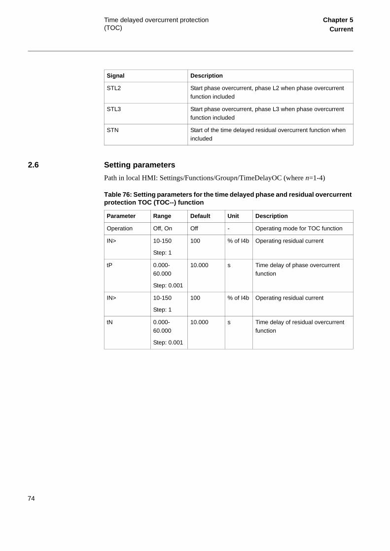
2.6 Setting parameters
Path in local HMI: Settings/Functions/Groupn/TimeDelayOC (where n=1-4)
Table 76: Setting parameters for the time delayed phase and residual overcurrent protection TOC (TOC--) function
STL2 Start phase overcurrent, phase L2 when phase overcurrent
function included
STL3 Start phase overcurrent, phase L3 when phase overcurrent
function included
STN Start of the time delayed residual overcurrent function when included
Signal Description
Parameter Range Default Unit Description
Operation Off, On Off - Operating mode for TOC function
IN> 10-150
Step: 1
100 % of I4b Operating residual current
tP 0.000-60.000
Step: 0.001
10.000 s Time delay of phase overcurrent function
IN> 10-150
Step: 1
100 % of I4b Operating residual current
tN 0.000-60.000
Step: 0.001
10.000 s Time delay of residual overcurrent function
74
Time delayed overcurrent protection (TOC)
Chapter 5Current
2.7 Technical data
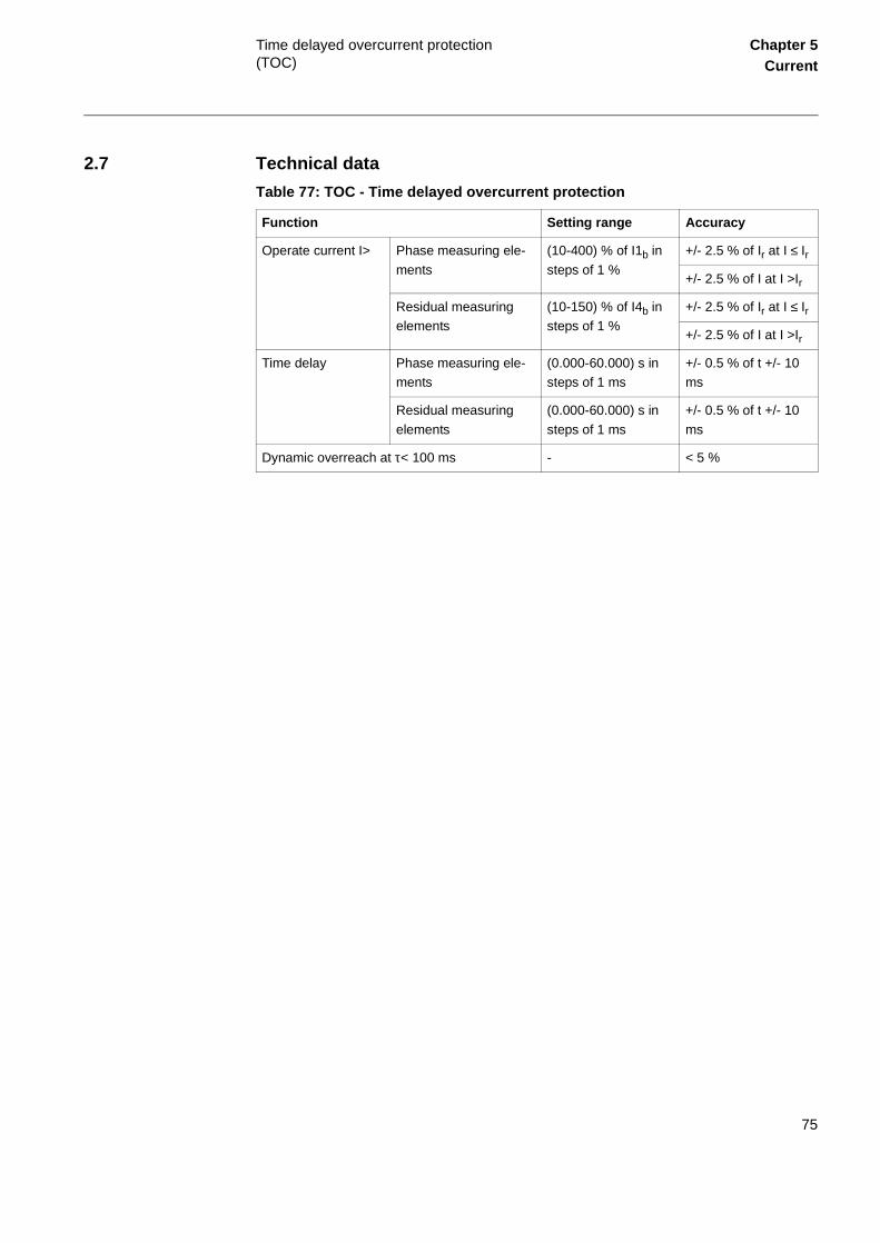
Table 77: TOC - Time delayed overcurrent protection
Function Setting range Accuracy
Operate current I> Phase measuring ele-
ments
(10-400) % of I1b in
steps of 1 %
+/- 2.5 % of Ir at I ≤ Ir
+/- 2.5 % of I at I >Ir
Residual measuring elements
(10-150) % of I4b in steps of 1 %
+/- 2.5 % of Ir at I ≤ Ir
+/- 2.5 % of I at I >Ir
Time delay Phase measuring ele-ments
(0.000-60.000) s in steps of 1 ms
+/- 0.5 % of t +/- 10 ms
Residual measuring
elements
(0.000-60.000) s in
steps of 1 ms
+/- 0.5 % of t +/- 10
ms
Dynamic overreach at τ< 100 ms - < 5 %
75
Two step time delayed phase overcurrent protection (TOC2)
Chapter 5Current
3 Two step time delayed phase overcurrent protection (TOC2)
3.1 Application
The two current/time stages of overcurrent protection TOC2 improve the possibility to get fast operation for nearby faults by using a high set current stage with short time de-lay. The low current stage is set with appropriate time delay to get selectivity with the adjacent relays in the system. In networks with inverse time delayed relays, selectivity is generally best obtained by using the same type of inverse time characteristic for all overcurrent relays.
3.2 Functionality
The current measuring element continuously measures the current in all three phases and compares it to the set operate value for the two current stages. A filter ensures im-munity to disturbances and DC components and minimizes the transient overreach. If the current in any of the three phases is above the set value I>Low, the start signal for the low current stage is activated. With setting Characteristic = Def, the timer tLow is activated and the trip signal TRLS is activated after set time. If inverse time delay is selected, the timer tMinInv starts when the current is above the set value I>Low. If the current also is above the set value I>Inv, the inverse time evaluation starts. When both time circuits operate, the definite time circuit tLow is activated and the trip signal TRLS is activated after the additional time tLow. If the current is above the set value I>High, the timer tHigh is activated and the trip signal TRHS is activated after set time.
The input signal BLOCK blocks all functions. Each current stage can also be individu-ally blocked.
3.3 Function block
TOC2-TOC2
BLOCKBLKTRLSBLKTRHS
TRLSTRHSSTLS
xx00000679.vsd
76
Two step time delayed phase overcurrent protection (TOC2)
Chapter 5Current
3.4 Logic diagram
Figure 30: Two step time delayed phase overcurrent protection, simplified logic dia-gram
3.5 Input and output signals
Table 78: Input signals for the TOC2 (TOC2-) function block
&
Characteristic = Def
Characteristic = NI/VI/EI/RI
& ≥1 t
tLow
& TOC2-TRLS
I>Inv
IL1-3I>Low
t
tMinInv
& TOC2-STLS
& t
tHigh& TOC2-TRHS
TOC2-BLOCK
TOC2-BLKTRLS
TOC2-BLKTRHS
t50 ms
I>High
&
&
en01000090.vsd
&
Signal Description
BLOCK Blocks the operation of both time delayed overcurrent stages.
BLKTRLS Blocks the trip from the definite or inverse time delayed low
current stage.
BLKTRHS Blocks the trip from the definite time delayed high set current stage
77
Two step time delayed phase overcurrent protection (TOC2)
Chapter 5Current
Table 79: Output signals for the TOC2 (TOC2-) two-step overcurrent function
3.6 Setting parameters
Table 80: Setting parameters for the two step time delayed phase overcurrent protection TOC2 (TOC2-) function
Signal Description
TRLS Trip from the definite or inverse time delayed low set current stage
TRHS Trip from the definite time delayed high set current stage
STLS Start of the low set current stage
Parameter Range Default Unit Description
Operation Off, On Off - Operating mode for TOC2 function
Operation Low Off, On On - Operating mode of low set TOC2 function
Characteristic Def, NI, VI, EI, RI
Def - Time delay characteristic for low set TOC2 function
I>Inv 5 - 500
Step: 1
10 % of I1b Base current for low set dependent
time delay operation
k 0.05 - 1.10
Step: 0.01
0.05 - Time multiplier for dependent time delay operation
tMinInv 0.000 - 60.000
Step: 0.001
0.050 s Minimum operating time for depen-dent time delay operation
I>Low 5-500
Step: 1
100 % of I1b Minimum operating current for dependent time delay operation
tLow 0.000 - 60.000
Step: 0.001
1.000 s Independent time delay for low set TOC2 function
78
Two step time delayed phase overcurrent protection (TOC2)
Chapter 5Current
3.7 Technical data
Table 81: TOC2 - Two step time delayed overcurrent protection
Operation High Off, On Off - Operating mode of high set TOC2
function
I>High 50-2000
Step: 1
100 % of I1b Operating current for high set TOC2
function
tHigh 0.000 - 60.000
Step: 0.001
1.000 s Time delay for high set TOC2 func-tion
Parameter Range Default Unit Description
Function Setting range Accuracy
Operate value for low set function (5-500)% of I1b in steps of
1%+/- 2.5% of I1r at
I <= I1r
+/- 2.5 % of I at I>I1r
Base current for inverse time
calculation
(5-500) % of I1b in steps of 1
%
+/- 2.5 % of I1r at
I <= I1r
+/- 2.5 % of I at I> I1r
Minimum operate time (0.000-60.000)s in steps of 1 ms
+/- 0.5 % +/- 10 ms
Definite time delay for low set
function
(0.000-60.000)s in step of
1ms
+/- 0.5 % +/- 10 ms
Operate value of high set function
(50-2000)% of I1b in steps of 1 %
+/- 2.5% of I1r at
I <= I1r
+/- 2.5 % of I at I>I1r
Definite time delay for high
set function
(0.000-60.000) s in steps of
1 ms
+/- 0.5 % +/- 10 ms
Normal inverse characteristic
I = Imeas/Iset
IEC 60255-3 class 5+/- 60 ms
79
Two step time delayed phase overcurrent protection (TOC2)
Chapter 5Current
Very inverse characteristic IEC 60255-3 class 7.5+/- 60 ms
Extremely inverse character-
istic
IEC 60255-3 class 7.5+/- 60 ms
Dynamic overreach at t< 100 ms <5%
Function Setting range Accuracy
80
Two step time delayed directional phase overcurrent protection (TOC3)
Chapter 5Current
4 Two step time delayed directional phase overcurrent protection (TOC3)
4.1 Application
The two current/time stages of the TOC3 overcurrent protection, both with optional di-rectional (Forward release or Reverse block) or non-directional function, improve the possibility to obtain selective function of the overcurrent protection relative other relays even in meshed networks. It must be realized, however, that the setting of a phase over-current protection system in a meshed network can be very complicated and a large number of fault current calculations are needed. In some cases, it is not possible to ob-tain selectivity even when using directional overcurrent protection. In such cases it is suggested to use line differential protection or distance protection function.
4.2 Functionality
The current measuring element continuously measures the current in all three phases and compares it to the set operate value for the two current stages. A filter ensures im-munity to disturbances and dc components and minimizes the transient overreach. If the current in any of the three phases is above the set value I>Low, the start signal for the low current stage is activated. With setting Characteristic = Def, the timer tLow is acti-vated and the trip signal TRLS is activated after set time. If inverse time delay is select-ed, the timer tMinInv starts when the current is above the set value I>Low. If the current also is above the set value I>Inv, the inverse time evaluation starts. When both time cir-cuits operate, the definite time circuit tLow is activated and the trip signal TRLS is ac-tivated after set time.
If the current is above the set value I>High, the timer tHigh is activated and the trip sig-nal TRHS is activated after set time.The low and the high set current stages can indi-vidually be set directional or non-directional. Directional information is calculated from positive sequence polarization voltages and the phase currents. The polarization voltage contains memory voltage to ensure directional function at close-in three-phase faults. The directional element relay characteristic angle (RCA) and operate angle are settable in wide ranges.
The input signal BLOCK blocks all functions. Trip from each current stage can also be individually blocked.
81
Two step time delayed directional phase overcurrent protection (TOC3)
Chapter 5Current
4.3 Function block
4.4 Logic diagram
Figure 31: Simplified block diagram for definite and inverse time delayed phase over-current function
TOC3BLOCKBLKTRLSBLKTRHS
TRLSTRHS
STNDLSSTND
STNDL1STNDL2STNDL3
STFWSTRV
xx00000198.vsd
I>Inv
NI, VI, EI, RI
IL1 (IL2, IL3)
I>Low
I>High
k, I>Inv
STLSL1-int (L2,L3)
STINVL1-int (L2,L3)
STHSL1-int (L2,L3)
en01000175.vsd
Characteristic= Def/NI/VI/EI/RI
82
Two step time delayed directional phase overcurrent protection (TOC3)
Chapter 5Current
Figure 32: Excerpt from directional phase selection
Figure 33: Current reversal logic for one phase and one set step
PE FAULT
PP FAULT &
>1
>1
&
>1
>1
DFWL1 - int.
DFWL1 - int.
DFWL2 - int.
L1L2
L1
L3L1
L1L2
L2
L2L3STLSL1 - intSTHSL1 - int
STLSL2 - intSTHSL2 - int
DIRFWL1L2 - int
DIRFWL1N - int
&
en01000154.vsd
DFW L1 - int&
DRVL1 - int &
FW L1 - int.t
50 ms
t50 ms
RVL1 - int.
STLSL1 - int
en01000155.vsd
≥1
&
83
Two step time delayed directional phase overcurrent protection (TOC3)
Chapter 5Current
Figure 34: Directional modes of TOC3
Figure 35: Delayed time operation for low set step and general time delay
STARTLSL1-int.STLSL1-intFWL1-int
Operation (Low) = ForwRelease
STARTLSL1-int.STLSL1-intRVL1-int
Operation (Low) = RevBlock
STARTLSL1-int.STLSL1-int
Operation (Low) = NonDir
en01000156.vsd
&
&
en01000157.vsd
STARTLSL1-intTRLSL1-int.
STINVL1-int
STARTHSL1-int TRHSL1-int.
High set step
Low set step&
&
≥1ttMinInv
ttHigh
t
tLow
Characteristic = Def
84
Two step time delayed directional phase overcurrent protection (TOC3)
Chapter 5Current
Figure 36: General trip
Figure 37: Start signals
TOC3--BLKTRLS
TOC3--TRLSTRLSL1-int
TOC3--BLOCK
TOC3--BLKTRHS
TRLSL3-intTRLSL2-int &
TOC3--TRHSTRHSL1-int
TRHSL3-intTRHSL2-int
&
t50 ms
en01000158.vsd
≥1
≥1
STLSL1-intTOC3--STNDL1STHSL1-int
STLSL2-intSTHSL2-int
STLSL3-intSTHSL3-int >1
>1
>1
>1
>1
&
TOC3--STNDL2&
TOC3--STNDL3&
TOC3--STNDLS&
TOC3--STND&
&
&>1
>1
TOC3--STFW&
TOC3--STRV&
FW L1-int
RVL1-int
TOC3--BLOCK
FW L2-int
RVL2-int
FW L3-int
RVL3-int
L3L2
L3L2L1
L1
t50 ms
en01000159.vsd
85
Two step time delayed directional phase overcurrent protection (TOC3)
Chapter 5Current
4.5 Input and output signals
Table 82: Input signals for the TOC3 (TOC3-) function block
Table 83: Output signals for the TOC3 (TOC3-) function block
Signal Description
BLOCK Blocks the time delayed overcurrent function
BLKTRLS Block the trip from the definite or inverse time delayed low current stage
BLKTRHS Blocks the trip from the definite time delayed high current
stage
Signal Description
TRLS Trip from the definite or inverse time delayed low current stage
TRHS Trip from the definite time delayed high current stage
STNDLS Non directional start for the low current stage
STND General non directional start
STNDL1 General non directional start, phase L1
STNDL2 General non directional start, phase L2
STNDL3 General non directional start, phase L3
STFW Operation of the forward directional element
STRV Operation of the reverse directional element
86
Two step time delayed directional phase overcurrent protection (TOC3)
Chapter 5Current
4.6 Setting parameters
Table 84: Setting parameters for the directional inverse time phase overcurrent protection TOC3 (TOC3-) function
Parameter Range Default Unit Description
Operation On/Off Off Operating mode for TOC3 function
Operation Low Off, Non-Dir, For-wRelease,
RevBlock
Off - Operation mode of low set step
Characteristic Def, NI, VI, EI, RI
Def - Time characteristic for low set step
I>Inv (20 - 500)
Step: 1
20 % of I1b Inverse time base current for low set step
k 0.050 - 1.100
Step: 0.010
0.050 Inverse time multiplier for low set step
tMinInv 0.000 - 60.000
Step: 0.001
0.050 s Inverse time minimum operating time for low set step
I>Low 20 - 2000
Step: 1
100 % of I1b Operating current/inverse time min.
current low set step
tLow 0.000 - 60.000
Step: 0.001
1.000 s Independent time delay for lowset
Operation High Off, Non-
Dir, For-wRelease, RevBlock
Off - Operation mode of high set step
I>High 20 - 2000
Step: 1
100 % of I1b Operating current for high set step
87
Two step time delayed directional phase overcurrent protection (TOC3)
115 degrees Upper angle of forward direction Characteristic
Parameter Range Default Unit Description
Function Setting range Accuracy
Operate value of low set func-tion
(20-2000)% of I1b in steps of 1% +/- 2.5 % of Ir at
I ≤ Ir
+/- 2.5 % of I at I>Ir
Base current for inverse time calculation
(20-500) % of I1b in steps of 1 % +/- 2.5 % of Ir at
I ≤ Ir
+/- 2.5 % of I at I>Ir
Minimum operate time (0.000-60.000) s in steps of 1 ms +/- 0.5 % +/- 10 ms
Definite time delay for low set function
(0.000-60.000) s in step of 1ms
+/- 0.5 % +/- 10 ms
Operate value of high set func-tion
(20-2000) % of I1b in steps of 1 % +/- 2.5 % of Ir at
I ≤ Ir
+/- 2.5 % of I at I>Ir
Definite time delay for high set
function
(0.000-60.000) in steps of 1 ms
+/- 0.5 % +/- 10 ms
Static angular accuracy at 0 degrees and 85 degrees
Voltage range (0.1-1.1) x Ur +/- 5 degrees
Current range (0.5-30) x Ir
Normal inverse characteristic
I = Imeas/Iset
IEC 60255-3 class 5 +/- 60
ms
88
Two step time delayed directional phase overcurrent protection (TOC3)
Chapter 5Current
Very inverse characteristic IEC 60255-3 class 7.5 +/-
60 ms
Extremely inverse characteris-
tic
IEC 60255-3 class 7.5 +/-
60 ms
Dynamic overreach at t< 100 ms <5%
Function Setting range Accuracy
89
Definite and inverse time-delayed residual overcurrent protection (TEF)
Chapter 5Current
5 Definite and inverse time-delayed residual overcurrent protection (TEF)
5.1 Application
Use the dependent and independent time delayed residual overcurrent functions in sol-idly earthed systems to get a sensitive and fast fault clearance of phase to earth faults.
The nondirectional protection can be used when high sensitivity for earth fault protec-tion is required. It offers also a very fast back-up earth fault protection for the part of a transmission line, closest to the substation with the protection.
The nondirectional residual overcurrent protection can be given a relatively low current pick-up setting. Thus the protection will be sensitive, in order to detect high resistive phase to earth faults.
The directional residual overcurrent protection can be used in a number of applications:
1. Main protection for phase to earth faults on the radial lines in solidly earthed sys-tems. Selectivity is achieved by using time delayed function according to practices in the system (independent time delay or some type of dependent time characteris-tic).
2. Main protection for phase to earth faults on lines in a meshed solidly earthed system. The directional function can be used in an permissive overreach communication scheme or a blocking scheme. In this application the directional residual overcurrent function is used together with the communication logic for residual overcurrent pro-tection.
3. Back-up protection for phase to earth faults for lines in solidly earthed systems. By using the directional residual protection as back-up function, the back-up fault clear-ance time can be kept relatively short together with the maintained selectivity.
4. Etc.
5.2 Functionality
The residual overcurrent protection (TEF) measures the residual current of the protect-ed line. This current is compared to the current settings of the function. If the residual current is larger than the setting value a trip signal will be sent to the output after a set delay time. The time delay can be selected between the independent or dependent pos-sibility.
90
Definite and inverse time-delayed residual overcurrent protection (TEF)
Chapter 5Current
(re-g cur-
In order to avoid unwanted trip for transformer inrush currents, the function is blocked if the second harmonic of the residual current is larger than 20% of the measured resid-ual current.
As an option the residual overcurrent protection can have directional function. The re-sidual voltage is used as a polarizing quantity. This voltage is either derived as the vec-torial sum of inputs U1+U2+U3 or as the input U4. The fault is defined to be in the forward direction if the residual current component in the characteristic angle 65°sidual current lagging the reference voltage, -3U0), is larger than the set operatinrent in forward direction. The same kind of measurement is performed also in thereverse direction.
5.3 Function block
Figure 38: Function block, directional and nondirectional
Figure 39: Function block, nondirectional
xx00000203.vsd
TEF--TEF
BLOCKBLKTRBC
TRIPTRSOTF
STARTSTFWSTRV
xx00000701.vsd
TEF--TEF
BLOCKBLKTRBC
TRIPTRSOTF
START
91
Definite and inverse time-delayed residual overcurrent protection (TEF)
Chapter 5Current
5.4 Logic diagram
Figure 40: Simplified logic diagram for the residual overcurrent protection
99000204.vsd
Operation = ON
Def/NI/VI/EI/LOG
&
&
>1
EFCh
k
IN>
±Σ
300mst
1000mst
3Io>
ttMin
&
tt1
&
IMin
20%
&
&
50mst
TEF--TRIP
= Directional
100% FORWARD
60% REVERSE
3Ioxcos (φ-65)
EF3IoSTD
0.01Un
2fn
2fn
Direction
Option: Directional check
3Uo
TEF--BLOCK
&
&
&
&
&
TEF--TRSOTF
TEF--STFW
TEF--STRV
TEF--START
TEF--BC
TEF--BLKTR
3Io
>1
92
Definite and inverse time-delayed residual overcurrent protection (TEF)
Chapter 5Current
5.5 Input and output signals
Table 86: Input signals for the TEF (TEF--) function block
Table 87: Output signals for the TEF (TEF--) function block
5.6 Setting parameters
Table 88: Settings for the TEF (TEF--) function
Signal Description
BLOCK Block of function
BLKTR Block of trip
BC Information on breaker position, or on breaker closing com-mand
Signal Description
TRIP Trip by TEF
TRSOTF Trip by earth fault switch onto fault function
START Non directional start
STFW Forward directional start
STRV Reverse directional start
Parameter Range Default Unit Description
Operation Off, On Off - Operating mode for TEF function
IMeasured I4, I5 I4 - Current signal used for earth fault function
Characteristic Def, NI, VI, EI, LOG
Def - Time delay characteristic for TEF protection
IN> 5 - 300
Step: 1
5 % of Inb Start current for TEF function (I4b or
I5b)
IMin 100 - 400
Step: 1
100 % of IN Minimum operating current
t1 0.000 - 60.000
Step: 0.001
0.000 s Independent time delay
93
Definite and inverse time-delayed residual overcurrent protection (TEF)
Chapter 5Current
5.7 Technical data
Table 89: Independent and dependent time delayed residual protection function
k 0.05 - 1.10
Step: 0.01
0.05 - Time multiplier for dependent time
delay
tMin 0.000 - 60.000
Step: 0.001
0.050 s Min. operating time for dependent time delay function
Direction NonDir, Directional
NonDir - Selection of directional or non direc-tional mode
UMeasured U4,
U+U2+U3
U4 - Voltage input used for directional
earth fault function
IN> Dir 5 - 35
Step: 1
5 % of Inb Start level for directional operation if selected (I4b or I5b)
Parameter Range Default Unit Description
Parameter Setting range Accuracy
Start current, definite time or inverse time delay 3I0
5-300% of Ir in steps of 1%
+/-5% of set value
Operate value
for directional current measure-ment
Forward 3I0
at ϕ=65 degrees
5-35% of Ir in steps
of 1%
+/-1.5% of Ir
Reverse 60% of the setting for forward operation
+/-1.5% of Ir
Definite time delay 0.000 - 60.000 s in steps of 1ms
+/- 0.5 % +/-10 ms
Normal inverse characteristic
I = Imeas/Iset
IEC 60255-3 class 5 +/- 60 ms
Very inverse characteristic IEC 60255-3 class 7.5 +/- 60 ms
Extremely inverse characteristic IEC 60255-3 class 7.5 +/- 60
ms
Min. operate current for dependent
characteristic
100-400% of 3I0 in
steps of 1%
+/-5% of Iset
94
Definite and inverse time-delayed residual overcurrent protection (TEF)
Chapter 5Current
Minimum operate time 0.000-60.000 s in step
of 1 ms
+/- 0.5 % +/-10 ms
Characteristic angles 65 degrees lagging +/-5 degrees at 20 V and
Iset=35% of Ir
Logarithmic characteristic +/- 5 % of t at I = (1.3-29) × 3I0
Minimum polarising voltage 1 % of Ur At 50 Hz: 1% of Ur +/-5%
At 60 Hz: 1% of Ur -15% to -5%
Reset time <70 ms -
Parameter Setting range Accuracy
t 5.8-1.35 ln I⋅=
95
Scheme communication logic for residual overcurrent protection (EFC)
Chapter 5Current
6 Scheme communication logic for residual overcurrent protection (EFC)
6.1 Application
The EFC directional comparison function contains logic for blocking overreaching and permissive overreaching schemes. The function is applicable together with TEF time delayed directional residual overcurrent protection in order to decrease the total operate time of a complete scheme.
One communication channel, which can transmit an on / off signal, is required in each direction. It is recommended to use the complementary additional communication logic EFCA, if the weak infeed and/or current reversal conditions are expected together with permissive overreaching scheme.
6.2 Functionality
The communication logic for residual overcurrent protection contains logics for block-ing overreach and permissive overreach schemes.
In the blocking scheme a signal is sent to the remote end of the line if the directional element, in the directional residual overcurrent protection (sending end), detects the fault in the reverse direction. If no blocking signal is received and the directional ele-ment, in the directional residual overcurrent protection (receiving end), detects the fault in the forward direction, a trip signal will be sent after a settable time delay.
In the permissive overreach scheme a signal is sent to the remote end of the line if the directional element, in the directional residual overcurrent protection (sending end), de-tects the fault in the forward direction. If an acceleration signal is received and the di-rectional element, in the directional residual overcurrent protection (receiving end), detects the fault in the forward direction, a trip signal will be sent, normally with no time delay. In case of risk for fault current reversal or weak end infeed, the additional logic for this should be used.
6.3 Function block
xx00000204
EFC--EFC
BLOCKCACCCSPRMCSBLKCR
TRIPCS
CRL
96
Scheme communication logic for residual overcurrent protection (EFC)
Chapter 5Current
6.4 Logic diagram
Figure 41: Simplified logic diagram, Scheme type = blocking
Figure 42: Simplified logic diagram, Scheme type = permissive
6.5 Input and output signals
Table 90: Input signals for the EFC (EFC--) function block
&
&
&
t 50 ms
t
0-60 s
t Coord
t25 ms
EFC-CSBLK
EFC-BLOCK
EFC-CACC
EFC-CR
EFC-CS
EFC-TRIP
EFC-CRL
99000107.vsd
&
&
&
&
&
t
0-60 s t
25 ms
>1
t
50 mst Coord
EFC-CRL
EFC-TRIP
EFC-CS
EFC-BLOCK
EFC-CR
EFC-CACC
EFC-CSBLK
EFC-CSPRM
99000108.vsd
Signal Description
BLOCK Block function
CACC Permits the operation when high
97
Scheme communication logic for residual overcurrent protection (EFC)
Chapter 5Current
Table 91: Output signals for the EFC (EFC--) function block
6.6 Setting parameters
Table 92: Setting parameters for the scheme communication logic EFC (EFC--) function
6.7 Technical data
Table 93: Scheme communication logic for residual overcurrent protection (EFC)
CSPRM Initiates sending of carrier signal in permissive scheme
CSBLK Initiates sending of carrier signal in blocking scheme
CR Information on received carrier signal
Signal Description
TRIP Trip by communication scheme logic
CS Carrier send by communication scheme logic
CRL Carrier receive by the communication scheme logic
Signal Description
Parameter Range Default Unit Description
Operation Off, On Off - Operating mode for EFC function
SchemeType Permis-sive, Block-ing
Permissive - Scheme type, mode of operation
tCoord 0.000-60.000
Step: 0.001
0.050 s Communication scheme coordina-tion time
Parameter Setting range Accuracy
Coordination timer 0.000-60.000 s in steps of 1 ms
+/-0.5% +/-10 ms
98
Current reversal and weak end infeed logic for residual overcurrent protection (EFCA)
Chapter 5Current
7 Current reversal and weak end infeed logic for residual overcurrent protection (EFCA)
7.1 Application
The EFCA additional communication logic is a supplement to the EFC scheme com-munication logic for the residual overcurrent protection.
To achieve fast fault clearing for all earth faults on the line, the TEF earth-fault protec-tion function can be supported with logic, that uses communication channels. REx 5xx terminals have for this reason available additions to scheme communication logic.
If parallel lines are connected to common busbars at both terminals, overreaching per-missive communication schemes can trip unselectively due to fault current reversal. This unwanted tripping affects the healthy line when a fault is cleared on the other line. This lack of security can result in a total loss of interconnection between the two bus-es.To avoid this type of disturbance, a fault current-reversal logic (transient blocking logic) can be used.
Permissive communication schemes for residual overcurrent protection, can basically operate only when the protection in the remote terminal can detect the fault. The detec-tion requires a sufficient minimum residual fault current, out from this terminal. The fault current can be too low due to an opened breaker or high positive and/or zero se-quence source impedance behind this terminal. To overcome these conditions, weak end infeed (WEI) echo logic is used.
7.2 Design
The reverse directed signal from the directional residual overcurrent function, starts the operation of a current reversal logic. The output signal, from the logic, will be activated, if the fault has been detected in reverse direction for more than the tPickUp time set on the corresponding timers. The tDelay timer delays the reset of the output signal. The signal blocks the operation of the overreach permissive scheme for residual current, and thus prevents unwanted operation due to fault current reversal.
The weak end infeed logic uses normally a forward and reverse signal from the direc-tional residual overcurrent function. The weak end infeed logic echoes back the re-ceived permissive signal, if none of the directional measuring elements have been activated during the last 200 ms. Further, it can be set to give signal to trip the breaker if the echo conditions are fulfilled and the residual voltage is above the set operate value for 3U0>.
99
Current reversal and weak end infeed logic for residual overcurrent protection (EFCA)
Chapter 5Current
7.3 Function block
7.4 Logic diagram
Figure 43: Simplified logic diagram, current reversal logic
Load currents that exceed the permissible continuous value may cause damage to the conductors and isolation due to overheating. The permissible load current will vary with the ambient temperature.
The THOL thermal overcurrent function supervises the phase currents and provides a reliable protection against damage caused by excessive currents. The temperature com-pensation gives a reliable thermal protection even when the ambient temperature varies largely.
8.2 Functionality
The final temperature rise of an object relative the ambient temperature is proportional to the square of the current. The rate of temperature rise is determined by the magnitude of the current and the thermal time constant of the object. The same time constant de-termines the rate of temperature decrease when the current is decreased.
The thermal overload function uses the highest phase current. The temperature change is continuously calculated and added to the figure for the temperature stored in the ther-mal memory. When temperature compensation is used, the ambient temperature is add-ed to the calculated temperature rise. If no compensation is used, 20o C is added as a fixed value. The calculated temperature of the object is then compared to the set values for alarm and trip.
The information on the ambient temperature is received via a transducer input 0 - 10 mA or 4 - 20 mA.
The output signal THOL--TRIP has a duration of 50 ms. The output signal THOL--START remains activated as long as the calculated temperature is higher than the set trip value minus a settable temperature difference TdReset (hysteresis). The output sig-nal THOL--ALARM has a fixed hysteresis of 5o C.
Table 103: Thermal overload protection mA input - Settings only via SMS or PST
Function Setting range Accuracy
Upper value for mA input
MI11-1_Max -25.00 - 25.00 mA in steps of 0.01 mA
+/- 0.5% of set value
Lower value for mA input
MI11-I_Min
-25.00 - 25.00 mA in steps of
0.01 mA
+/- 0.5% of set value
Temp. corresponding to the MI11-1_Max setting
MI11-MaxValue-1000 - 1000 °C in steps of 1 oC
+/- 1% of set value +/- 1°C
Temp. corresponding to the MI11-1_Min setting
MI11-MinValue-1000 - 1000° C in steps of 1 °C
+/- 1% of set value +/- 1°C
107
Breaker failure protection (BFP) Chapter 5Current
9 Breaker failure protection (BFP)
9.1 Application
In many protection applications local redundancy is used. One part of the fault clear-ance system is however never duplicated, namely the circuit breaker. Therefor a breaker failure protection can be used.
The breaker failure protection is initiated by trip signals from different protection func-tions within or outside the protection terminal. When a trip signal is sent to the breaker failure protection first, with no or a very short delay, a re-trip signal can be sent to the protected breaker. If fault current is flowing through the breaker still after a setting time a back-up trip signal is sent to the adjacent breakers. This will ensure fault clearance also if the circuit breaker is out of order.
9.2 Design
The breaker failure protection function is initiated by the trip commands from protec-tion functions placed either inside the same terminal or externally, by connection to ap-propriate binary inputs. Three separate functional inputs are available for single-phase starting. A dedicated input is available also for three-phase starting.
The operate value of the phase segregated current measuring elements is settable within a wide range. Three independent timers t2 are available for phase segregated breaker failure detection.
An additional timer t1 for retrip command is available. Dedicated setting allows to en-able or disable the retrip or to perform it by current check or not. Retrip to the faulty circuit breaker can be issued single phase or three phase.
Special adaptive algorithm (ASD), together with RMS measurement, allow a fast reset-ting time of the current measuring elements. The current measurement is stabilised against transients which can cause unwanted operation with saturated current trans-formers.
Table 104: Input signals for the breaker failure protection (BFP--) function block
STIL3
BFP-STL3
BFP-START≥1
&
&
BFP-TRRETL3
tp
tp
BFP-TRBU
STIL2
BFP-STL2
BFP-START≥1
&
&
BFP-TRRETL2
tp
Block BFP=Yes
TEST-ACTIVE
BFP-BLOCK
≥1
STIL1
BFP-STL1
BFP-START
&
≥1
&
&
&
BFP-TRRETL1
tp≥1
≥1 BFP-TRRET
RETRIP=No I>Check
RETRIP=I>Check
t
t2
t
t2
t
t2
t
t1
t
t1
t
t1
&
&
en01000185.vsd
TEST
Signal Description
BLOCK Block function
START Start function
STL1 Start phase L1
STL2 Start phase L2
STL3 Start phase L3
109
Breaker failure protection (BFP) Chapter 5Current
Table 105: Output signals for the breaker failure protection BFP (BFP--) function block
9.6 Setting parameters
Table 106: Setting parameters for the breaker failure protection BFP (BFP--) func-tion
Signal Description
TRBU Backup trip
TRRET Retrip
TRRETL1 Retrip by phase L1
TRRETL2 Retrip by phase L2
TRRETL3 Retrip by phase L3
Parameter Range Default Unit Description
Operation Off, On Off Operating mode for BFP function
IP> 5-200
Step: 1
100 % of I1b Operating phase current
t2 0.000-60.000
Step: 0.001
0.200 s Delay timer for backup trip
RetripType Retrip Off,
I> Check, No I> Check
Retrip Off Operating mode of retrip logic
t1 0.000-60.000
Step: 0.001
0.050 s Delay timer for retrip
110
Breaker failure protection (BFP) Chapter 5Current
9.7 Technical data
Table 107: Breaker failure protection
Parameter Setting range Accuracy
Operate current (one mea-
suring element per phase)
5-200% of I1b in steps of 1% +/-2.5% of Ir at I ≤ Ir
+/-2.5% of I at I > Ir
Retrip time delay t1 0.000-60.000 s in steps of 1 ms
+/-0.5% of setting +/-10 ms
Back-up trip time delay t2 0.000-60.000 s in steps of 1 ms
+/-0.5% of setting +/-10 ms
Parameter Value
Trip operate time Max 18 ms
Reset time Max 10 ms
111
Unbalance protection for capacitor banks (TOCC)
Chapter 5Current
10 Unbalance protection for capacitor banks (TOCC)
10.1 Application
Capacitor banks are made up of individual units which are series and parallel connected. Each unit is made up of several series and parallel connected elements. If one element is short-circuited or disconnected by internal fuses, the load on the remaining elements increases.The unbalance protection is connected to a current transformer which mea-sures the current flowing between two normally balanced parts of the capacitor bank. Under normal conditions, no current flows in the interconnection. A low set current stage gives alarm when elements are damaged and current flows in the interconnection. The trip stage is set to disconnect the bank before healthy elements become overloaded and damaged.
10.2 Functionality
The current measuring element continuously measures the unbalance current and com-pares it to the set operate value for the two current stages. A filter ensures immunity to disturbances and harmonic currents.The output relay for the low current (alarm) stage operates if the current becomes higher than the set operate value ILow during a time exceeding the set time delay tLow. If the current becomes higher than the set operate value IHigh during a time exceeding the set time delay tHigh, the output relay for the high current stage operates.
The input signal BLOCK blocks both the low set and the high set functions.
10.3 Function block
xx00000635.vsd
TOCC-TOCC
BLOCK TRLSTRHS
112
Unbalance protection for capacitor banks (TOCC)
Chapter 5Current
10.4 Logic diagram
Figure 48: Unbalance protection for capacitor banks, simplified logic diagram
10.5 Input and output signals
Table 108: Input signals for the TOCC (TOCC-) function block
Table 109: Output signals for the TOCC (TOCC-) function block
TOCC-BLOCK
LOW
I>
High
&
&
t
tLow
t
tHigh
TOCC-TRLS
TOCC-TRHS
I
xx01000091.vsd
Signal Description
BLOCK Blocks the unbalance protection function
Signal Description
TRLS Alarm from the low set current stage
TRHS Trip from the high set current stage
113
Unbalance protection for capacitor banks (TOCC)
Chapter 5Current
10.6 Setting parameters
Table 110: Setting parameters for the TOCC (TOCC-) function
10.7 Technical data
Table 111: TOCC- Unbalance protection
Parameter Range Default Unit Description
Operation Low On/Off Off - Operating mode of the low set cur-
rent function
I>Low 2-100
Step: 1
30 % of I5b Operate value of the low set current function
tLow 0.000-
60.000
Step: 0.001
5.000 s Time delay of the low set current
function
Operation High On/Off Off - Operating mode of the high set cur-rent function
I>High 2-100
Step: 1
30 % of I5b Operate value of the high set current function
tHigh 0.000-60.000
Step: 0.001
5.000 s Time delay of the high set current function
Function Setting range Accuracy
Operate current of low set
stage I>Low
(2-100) % of I5b in steps of 1% +/- 5 % of Ir
Time delay tLow of current stage I>Low
(0.000-60.000) s in steps of 1ms
+/- 0.5 % of t +/- 10 ms
Operate current of high set stage I>High
(2-200) % of I5b in steps of 1% +/- 5 % of Ir
Time delay tHigh of current
stage I>High
(0.000-60.000) s in steps of
1ms
+/- 0.5 % of t +/- 10 ms
114
About this chapter Chapter 6Voltage
Chapter 6 Voltage
About this chapter
This chapter describes the voltage protection functions.
115
Time delayed undervoltage protection (TUV)
Chapter 6Voltage
1 Time delayed undervoltage protection (TUV)
1.1 Application
The time delayed undervoltage protection function, TUV, is applicable in all situations, where reliable detection of low phase voltages is necessary. The function can also be used as a supervision and fault detection function for some other protection functions, to increase the security of a complete protection system.
Table 112: Input signals for the TUV (TUV--) function block
Table 113: Output signals for the TUV (TUV--) function block
1.5 Setting parameters
Table 114: Setting parameters for the time delayed undervoltage protection TUV (TUV--) function
Signal Description
BLOCK Block undervoltage function
BLKTR Block of trip from time delayed undervoltage function
VTSU Block from voltage transformer circuit supervision
Signal Description
TRIP Trip by time delayed undervoltage function
STL1 Start phase undervoltage phase L1
STL2 Start phase undervoltage phase L2
STL3 Start phase undervoltage phase L3
START Start phase undervoltage
Parameter Range Default Unit Description
Operation Off, On Off - Operating mode for TUV function
UPE< 10-100
Step: 1
70 % of U1b
Operate phase voltage
t 0.000-60.000
Step: 0.001
0.000 s Time delay
117
Time delayed undervoltage protection (TUV)
Chapter 6Voltage
1.6 Technical data
Table 115: TUV - Time delayed undervoltage protection
Function Setting range Accuracy
Operate voltage U< (10-100) % of U1b in steps of
1%
+/- 2.5 % of Ur
Time delay (0.000-60.000) s in steps of 1ms
+/- 0.5 % +/- 10 ms
118
Time delayed overvoltage protection (TOV)
Chapter 6Voltage
2 Time delayed overvoltage protection (TOV)
2.1 Application
The time delayed phase overvoltage protection is used to protect the electrical equip-ment and its insulation against overvoltage by measuring three phase voltages. In this way, it prevents the damage to the exposed primary and secondary equipment in the power systems.
The residual overvoltage protection function is mainly used in distribution networks, mainly as a backup protection for the residual overcurrent protection in the line feeders, to secure the disconnection of earth-faults.
2.2 Functionality
The phase overvoltage protection function continuously measures the three phase volt-ages and initiates the corresponding output signals if the measured phase voltages ex-ceed the preset value (starting) and remain high longer than the time delay setting on the timers (trip). This function also detects the phases which caused the operation.
The residual overvoltage protection function calculates the residual voltage (3U0) from the measuring three phase voltages and initiates the corresponding output signals if the residual voltage is larger than the preset value (starting) and remains high longer than the time delay setting (trip).
2.3 Function block
Figure 50: TOV function block, phase and residual overvoltage
xx00000217.vsd
TOV--TOV
BLOCKBLKTR
TRIPTRPE
TRNSTPESTL1STL2STL3STN
119
Time delayed overvoltage protection (TOV)
Chapter 6Voltage
Figure 51: TOV function block phase overvoltage
Figure 52: TOV function block residual overvoltage
xx00000686.vsd
TOV--TOV
BLOCKBLKTR
TRIPTRPESTPESTL1STL2STL3
xx00000687.vsd
TOV--TOV
BLOCKBLKTR
TRIPTRNSTN
120
Time delayed overvoltage protection (TOV)
Chapter 6Voltage
2.4 Logic diagram
Figure 53: TOV, logic diagram
2.5 Input and output signals
Table 116: Input signals for the TOV (TOV--) function block
Table 117: Output signals for the time delayed overvoltage protection TOV (TOV--) function
en01000187.vsd
TOV--BLKTR
TOV--BLOCK
TOV--TEST
Block TOV=Yes
TOV--STUL1N
TOV--STUL2N
TOV--STUL3N
&
&
TOV--TRIP
TOV--TRPE
TOV--STPE
TOV--STL1
TOV--STL2
TOV--STL3
TEST
&
&
&
TOV--ST3UO & &
TOV--STN
TOV--TRN
≥1
t
t
≥1
≥1
Signal Description
BLOCK Block of time delayed overvoltage function
BLKTR Block of trip output from time delayed overvoltage function
Signal Description
TRIP General trip output from TOV function block
TRPE Trip by phase overvoltage function
TRN Trip by residual overvoltage function
121
Time delayed overvoltage protection (TOV)
Chapter 6Voltage
2.6 Setting parameters
Table 118: Setting parameters for time delayed overvoltage TOV (TOV--) function
STPE Start phase overvoltage function
STL1 Start phase overvoltage phase L1
STL2 Start phase overvoltage phase L2
STL3 Start phase overvoltage phase L3
STN Start by residual overvoltage function
Signal Description
Parameter Range Default Unit Description
Operation Off, On Off - Operating mode for TOV function
UPE> 50-200
Step: 1
120 % of
U1b
Operate value for the phase over-
voltage function
t 0.000-60.000
Step: 0.001
0.000 s Time delay of the phase overvoltage function
3U0> 5-100
Step: 1
30 % of
U1b
Operate value for the neutral over-
voltage function
t 0.000-60.000
Step: 0.001
0.000 s Time delay of the neutral overvolt-age function
122
Time delayed overvoltage protection (TOV)
Chapter 6Voltage
2.7 Technical data
Table 119: TOV - Time delayed overvoltage protection
If a conductor in the 50 Hz system comes into contact with the conductor of a 16 2/3 Hz system with higher nominal voltage, the 16 2/3 Hz voltage must quickly be disconnect-ed to avoid damage on the power transformer and other components in the 50 Hz sys-tem.
The protection is connected to measure the phase-to-ground voltage of the 50 Hz con-ductor. The operate voltage must, with margin, be set higher than the 16 2/3 Hz voltage normally induced in the 50 Hz circuit.
3.2 Functionality
The voltage measuring element continuously measures the 16 2/3 Hz voltage compo-nent and compares it to the set operate value U>. A filter ensures immunity to distur-bances and harmonic voltages and reduces the influence of the 50 Hz voltage component with a factor > 10.The output trip relay operates if the voltage becomes higher than the set operate value U> under a time exceeding the set definite time delay t.
About this chapter Chapter 7Power system supervision
Chapter 7 Power system supervision
About this chapter
This chapter describes the power system supervision functions.
127
Loss of voltage check (LOV) Chapter 7Power system supervision
1 Loss of voltage check (LOV)
1.1 Application
The loss of voltage detection, LOV, is suitable for use in networks with an automatic restoration function. The LOV function issues a three-pole trip command to the circuit breaker, if all three phase voltages fall below the set value for a time longer than 7 sec-onds, and the circuit breaker remains closed.
1.2 Functionality
The operation of LOV function is based on line voltage measurement. The function is provided with a logic, which automatically recognises if the line was restored for at least three seconds before starting the seven seconds timer. Additionally, the function is automatically blocked if only one or two phase voltages have been detected low for more than 10 seconds. The LOV function operates again only if the line has been fully energised.
Operation of LOV function is also inhibited by fuse failure and open circuit breaker in-formation signals, by their connection to dedicated inputs of the function block.
The operation of the function is supervised by the fuse-failure function and the infor-mation about the closed position of the associated circuit breaker.
1.3 Function block
xx00000209.vsd
LOV--LOV
BLOCKCBOPENVTSU
TRIP
128
Loss of voltage check (LOV) Chapter 7Power system supervision
1.4 Logic diagram
Figure 55: Simplified logic diagram of loss of voltage check protection function
1.5 Input and output signals
Table 124: Input signals for the LOV (LOV--) function block
LOV--BLOCK
LOV--TRIPFunction Enable
LOV - LOSS OF VOLTAGE CHECK FUNCTION
TEST-ACTIVE
&
TEST
BlockLOV = Yes
>1
STUL1N
STUL2N
STUL3N
LOV--CBOPEN
t
7 s 150 ms
&
LOV--VTSU
&
>1 t
10 s
&
only 1 or 2 phases are low forat least 10 s (not three)
>1 &
>1t
3 s
Reset Enable
Set Enable>1
Line restored forat least 3 s
LatchedEnable
99000488.vsd
Signal Description
BLOCK Block of loss of voltage check
CBOPEN Circuit breaker open
VTSU Block of loss of voltage check from voltage circuit supervision
129
Loss of voltage check (LOV) Chapter 7Power system supervision
Table 125: Output signals for the LOV (LOV--) function block
1.6 Setting parameters
Table 126: Setting parameters for the loss of voltage check LOV (LOV--) function
1.7 Technical data
Table 127: Loss of voltage check
Signal Description
TRIP Trip by loss of voltage check
Parameter Range Default Unit Description
Operation Off, On Off - Operating mode for LOV function
UPE< 10-100
Step: 1
70 % of U1b
Operating phase voltage
Parameter Setting range Accuracy
Operate voltage, U< 10-100% of U1b in steps of 1% +/-2.5% of Ur
130
Dead line detection (DLD) Chapter 7Power system supervision
2 Dead line detection (DLD)
2.1 Application
The main purpose of the dead line detection is to provide different protection, control and monitoring functions with the status of the line, i.e whether or not it is connected to the rest of the power system
2.2 Functionality
The dead line detection function continuously measures all three phase currents and phase voltages of a protected power line. The line is declared as dead (not energized) if all three measured currents and voltages fall below the preset values for more than 200 ms.
2.3 Function block
xx00000189.vsd
DLD--DLD
BLOCK STARTSTIL1STIL2STIL3
STUL1STUL2STUL3STPH
131
Dead line detection (DLD) Chapter 7Power system supervision
2.4 Logic diagram
Figure 56: DLD - simplified logic diagram of a function
2.5 Input and output signals
Table 128: Input signals for the DLD (DLD--) function block
en00000493.vsd
&
&
&
&
&
&
&
&
>1
&
&
&
&
STUL3N
STUL1N
STMIL3
STUL2N
STMIL2
STMIL1 DLD--STIL1
DLD--STIL2
DLD--STIL3
DLD--STUL1
DLD--STUL2
DLD--STUL3
DLD--STPH
DLD--START
DLD--BLOCK
Signal Description
BLOCK Block of dead line detection
132
Dead line detection (DLD) Chapter 7Power system supervision
Table 129: Output signals for the DLD (DLD--) function block
2.6 Setting parameters
Table 130: Setting parameters for the dead line detection DLD (DLD--) function
2.7 Technical data
Table 131: DLD - Dead line detection
Signal Description
START Dead line condition detected in all three phases
STIL1 Current below set value phase L1
STIL2 Current below set value phase L2
STIL3 Current below set value phase L3
STUL1 Voltage below set value phase L1
STUL2 Voltage below set value phase L2
STUL3 Voltage below set value phase L3
STPH Dead phase condition detected in at least one phase
Parameter Range Default Unit Description
Operation Off / On Off - Operating mode for DLD function
U< 10 - 100
Step: 1
70 % of
U1b
Operating phase voltage (undervolt-
age function)
IP< 5 - 100
Step: 1
20 % of I1b Operating phase current (undercur-rent function)
Function Setting range Accuracy
Automatic check of dead line condition
Operate phase current (5-100) % of I1b in steps of 1%
+/- 2.5 % of Ir
Operate phase voltage (10-100) % of U1b in
steps of 1%
+/- 2.5 % of
Ur
133
Dead line detection (DLD) Chapter 7Power system supervision
134
About this chapter Chapter 8Secondary system supervision
Chapter 8 Secondary system supervision
About this chapter
This chapter describes the secondary system supervision functions
135
Fuse failure supervision (FUSE) Chapter 8Secondary system supervision
1 Fuse failure supervision (FUSE)
1.1 Application
The fuse failure supervision function, FUSE, continuously supervises the ac voltage cir-cuits between the voltage instrument transformers and the terminal. Different output signals can be used to block, in case of faults in the ac voltage secondary circuits, the operation of the distance protection and other voltage-dependent functions, such as the synchro-check function, undervoltage protection, etc.
Different measurement principles are available for the fuse failure supervision function.
The FUSE function based on zero sequence measurement principle, is recommended in directly or low impedance earthed systems.
The FUSE function based on the negative sequence measurement principle is recom-mended in isolated or high impedance earthed systems.
A criterion based on delta current and delta voltage measurements can be added to the FUSE function in order to detect a three phase fuse failure, which in practice is more associated with voltage transformer switching during station operations.
1.2 Functionality
The FUSE function based on the negative sequence measurement principle continuous-ly measures the negative sequence voltage and current in all three phases. It operates if the measured negative sequence voltage increases over the preset operating value, and if the measured negative sequence current remains below the preset operating value.
The FUSE function based on the zero sequence measurement principle continuously measures the zero sequence current and voltage in all three phases. It operates if the measured zero sequence voltage increases over preset operating value, and if the mea-sured zero sequence current remains below the preset operating value.
The delta current and delta voltage algorithm, detects a fuse failure if a sufficient neg-ative change in voltage amplitude without a sufficient change in current amplitude is detected in each phase separately. This check is performed if the circuit breaker is closed. Information about the circuit breaker position is brought to the function input CBCLOSED through a binary input of the terminal.
136
Fuse failure supervision (FUSE) Chapter 8Secondary system supervision
Three output signals are available. The first depends directly on the voltage and current measurement. The second depends on the operation of the dead line detection function, to prevent unwanted operation of the distance protection if the line has been deener-gised and energised under fuse failure conditions. The third depends on the loss of all three measured voltages. A special function input serves the connection to the auxiliary contact of a miniature circuit breaker, MCB (if used), to secure correct operation of the function on simultaneous interruption of all three measured phase voltages also when the additional delta current and delta voltage algorithm is not present in the function block.
1.3 Function block
Figure 57: Function block, FUSE function including DU/Dt based
Figure 58: Function block, negative sequence, zero sequence
xx00000212.vsd
FUSE-FUSE
BLOCKMCBDISCDLCNDCBCLOSED
VTSUVTSZ
VTF3PH
xx01000096.vsd
FUSE-FUSE
BLOCKMCBDISCDLCND
VTSUVTSZ
VTF3PH
137
Fuse failure supervision (FUSE) Chapter 8Secondary system supervision
Fuse failure supervision (FUSE) Chapter 8Secondary system supervision
Figure 60: Simplified logic diagram for fuse failure supervision function, zero sequence
Store in non volatile(FUSE-STORE3PH)
FUSE-BLOCK
FUSE-VTSU
99000500.vsd
FUSE - FUSE FAILURE SUPERVISION FUNCTION
TEST-ACTIVE&
TEST
BlockFUSE= Yes
STZERO
&
FUSE-VTSZ
FUSE-VTF3PH
FUSE-MCB
FUSE-DISC
&
&
t150 ms
FUSE-DLCNDt
200 ms
t5 s
&
STUL3N
STUL2N
STUL1N
&&
STORE3PH20 ms
1:All voltagesare low
From non volatilememory
0: All voltagesare high(Reset Latch)
1:Fuse failure formore than 5 s
Dead-LineBlock
(Set Latch)
1:Function Enable
1:Fuse FailureDetection
≥1
≥1
&
≥1
≥1
≥1
≥1
≥1
139
Fuse failure supervision (FUSE) Chapter 8Secondary system supervision
Figure 61: Simplified logic diagram for fuse failure supervision function, du/dt based
1.5 Input and output signals
Table 132: Input signals for the FUSE (FUSE-) function block
Store in non volatile(FUSE-STORE3PH)
FUSE-BLOCK
FUSE-VTSU
en01000097.vsd
FUSE - FUSE FAILURE SUPERVISION FUNCTION
TEST-ACTIVE
&
TEST
BlockFUSE= Yes
STDUDI
&
FUSE-VTSZ
FUSE-VTF3PH
FUSE-MCB
FUSE-DISC
&
&
t150 ms
>1
>1FUSE-DLCNDt
200 ms&
>1 t5 s&
STUL3N
STUL2N
STUL1N
>1
&& >1
>1
STORE3PH20 ms
>1
1:All voltagesare low
From non volatilememory
0: All voltagesare high (ResetLatch)
1:Fuse failure formore than 5 s
Dead-LineBlock
(Set Latch)
1:FunctionEnable
1:Fuse FailureDetection
STDUDIL1 &
&
&
&
STDUDIL2
STDUDIL3
FUSE-CBCLOSED
IL1>
IL2>
IL3>
&≥1
Signal Description
BLOCK Block of fuse failure function
MCB Operation of MCB
DISC Line disconnector position
DLCND Dead line condition
CBCLOSED Circuit breaker closed information
140
Fuse failure supervision (FUSE) Chapter 8Secondary system supervision
Table 133: Output signals for the FUSE (FUSE-) function block
1.6 Setting parameters
Table 134: Setting parameters for the fuse failure supervision FUSE (FUSE-) func-tion
Table 135: Setting parameters for the fuse failure supervision FUSE (FUSE-) func-tion
Signal Description
VTSU Block for voltage measuring functions
VTSZ Block for impedance measuring functions
VTF3PH Detection of 3-phase fuse failure
Parameter Range Default Unit Description
ZeroSeq Off, On Off - Operating mode for FUSE function
3U0> 10-50
Step: 1
10 % of U1b
Operating zero sequence voltage
3I0< 10-50
Step: 1
10 % of I1b Operating zero sequence current
Parameter Range Default Unit Description
NegativeSeq Off, On Off - Operating mode for FUSE function
3U2> 10-50
Step: 1
10 % of
U1b
Operating negative sequence volt-
age
3I2< 10-50
Step: 1
10 % of I1b Operating negative sequence cur-rent
141
Fuse failure supervision (FUSE) Chapter 8Secondary system supervision
Table 136: Setting parameters for the fuse failure supervision FUSE (FUSE-) func-tion, du/dt, di/dt based
1.7 Technical data
Table 137: FUSE - Fuse failure supervision function
Table 138: FUSE - Fuse failure supervision function
Table 139: Fuse failure supervision function
Parameter Range Default Unit Description
I> 10-50
Step: 1
10 % of I1b Operate phase current level
DU> 50-90
Step: 1
80 % of U1b
Operate voltage change level
DI< 10-50
Step: 1
10 % of I1b Operate current change level
Function Setting range Accuracy
Zero-sequence
quantities:
Operate voltage
3U0
(10-50)% of U1b in steps of
1%
+/- 2.5 % of Ur
Operate current 3I0
(10-50)% of I1b in steps of 1% +/- 2.5 % of Ir
Function Setting range Accuracy
Negative-sequence
quantities:
Operate voltage
3U2
(10 - 50)% of U1b in
steps of 1%
+/- 2.5 % of Ur
Operate current 3I2 (10 - 50)% of I1b in steps of 1%
+/- 2.5 % of Ir
Function Setting range Accuracy
Operate voltage change level (50-90)% of U1b in steps of
1%
+/-2.5% of Ur
Operate current change level (10-50)% of I1b in steps of 1% +/- 2.5% of Ir
142
Voltage transformer supervision (TCT) Chapter 8Secondary system supervision
2 Voltage transformer supervision (TCT)
2.1 Application
The main purpose of the voltage transformer supervision function is to indicate failure in the measuring voltage from a capacitive voltage transformer.
2.2 Functionality
The voltage transformer supervision function checks all of the three phase-phase volt-ages and the residual voltage. If the residual voltage exceeds the setpoint value and any of the phase-phase voltages is higher than 80% of the rated phase-phase voltage the out-put is activated after a settable time delay.
2.3 Function block
2.4 Logic diagram
Figure 62: Simplified logic diagram, TCT function
xx00000618.vsd
TCT--TCT
BLOCKVTSU
START
STUPP1
STUPP2
STUPP3
STUR
& START
en01000001.vsd
>1
BLOCK
VTSU 1
t
tDelay
&
>1
143
Voltage transformer supervision (TCT) Chapter 8Secondary system supervision
2.5 Input and output signals
Table 140: Input signals for the TCT (TCT--) function block
Table 141: Output signals for the TCT (TCT--) function block
2.6 Setting parameters
Table 142: Settings for the voltage transformer supervision TCT (TCT--) function
2.7 Technical data
Table 143: Voltage transformer supervision
Signal Description
BLOCK Block of voltage transformer supervision
VTSU Block of voltage transformer supervision from voltage circuit supervision
Signal Description
START Start by voltage transformer supervision
Parameter Range Default Unit Description
Operation On/Off Off - Operating mode for TCT function
UN> 1.0-80.0
Step: 0.1
10.0 % of
U1b
Residual overvoltage limit
tDelay 0.000-300.000
Step. 0.001
3.000 s Time delayed operation for start sig-nal
Parameter Setting range
Accuracy
Residual overvoltage limit, UN> 1.0-80.0% of
U1b in steps of 0.1%
+/- 2.5% of Ur
Time delayed operation for start signal, tDelay 0.000-
300.000 s in steps of 1 ms
+/- 0.5% +/- 10 ms
144
About this chapter Chapter 9Control
Chapter 9 Control
About this chapter
This chapter describes the control functions
145
Synchrocheck (SYN) Chapter 9Control
1 Synchrocheck (SYN)
1.1 Application
The main purpose of the synchrocheck function is to provide controlled closing of cir-cuit breakers in interconnected networks.
The main purpose of the energizing check function is to facilitate the controlled recon-nection of a disconnected line or bus to, respectively, an energized bus or line.
The main purpose of the phasing function is to provide controlled closing of circuit breakers when two asynchronous systems are going to be connected. It is used for slip frequencies that are larger than those for synchrocheck.
Note:
The phasing function is only available together with the synchrocheck and energizing check functions.
To meet the different application arrangements, a number of identical SYN function blocks may be provided within a single terminal. The number of these function blocks that may be included within any given terminal depends on the type of terminal. There-fore, the specific circuit breaker arrangements that can be catered for, or the number of bays of a specific arrangement that can be catered for, depends on the type of terminal.
1.2 Functionality
The synchrocheck function measures the conditions across the circuit breaker and com-pares them to set limits. The output is only given when all measured conditions are si-multaneously within their set limits.
The energizing check function measures the bus and line voltages and compares them to both high and low threshold detectors. The output is only given when the actual mea-sured conditions match the set conditions.
The phasing function measures the conditions across the circuit breaker, and also deter-mines the angle change during the closing delay of the circuit breaker from the mea-sured slip frequency. The output is only given when all measured conditions are simultaneously within their set limits. The issue of the output is timed to give closure at the optimal time.
146
Synchrocheck (SYN) Chapter 9Control
For single circuit breaker and 1 1/2 circuit breaker arrangements, the SYN function blocks have the capability to make the necessary voltage selection. For single circuit breaker arrangements, selection of the correct voltage is made using auxiliary contacts of the bus disconnectors. For 1 1/2 circuit breaker arrangements, correct voltage selec-tion is made using auxiliary contacts of the bus disconnectors as well as the circuit breakers (as well as binary output signals from the other terminals in the same diameter for 1 1/2 circuit breaker applications with a separate terminal per circuit breaker).
Figure 69: SYN, simplified logic diagram, synchrocheck and energizing check, The in-ternal signal UENERG1OK refers to the voltage selection logic.
en01000107.vsd
OPERATION OFF
RELEASE ON
UDiff
UBusHigh
ULineHigh
FreqDiff
PhaseDiff
SYN1-BLOCK
& t50 ms
& &
&
>1
>1
SYN1-AUTOOK
SYN1-MANOK
SYN1
AUTOENERG1
MANENERG1UDIFF
FRDIFF
PHDIFF
OFFBothDLLBDBLL
UL HighUL LowUB HighUB Low
AutoEnerg.
>1
>1
&
&
>1 t
50 mst
0.00-60.0s
OFFBothDLLBDBLL
>1
>1
&
&
>1&
>1
OFFON
ManDBDL
ManEnerg.
t
50 mst
0.00-60.0s
UENERG1OK
AUTOENERG1
MANENERG1
SYNCHROCHECK
ENERGIZING CHECK
&
&
150
Synchrocheck (SYN) Chapter 9Control
Figure 70: SYN, phasing, simplified logic diagram. The input signals SYN1-AUTOOK and SYN1-MANOK derive from the synchrocheck and energizing logic
OPERATION SYNCHOFFON
OFFON
TEST MODE
SYN1-START
SYN1-BLOCK >1
& SR
UDiff
UBusHigh
ULineHigh
FreqDiffSynch
FreqDiff
dF/dt Bus
dF/dt Line
Fbus ± 5 Hz
Fline ± 5 Hz
PhaseDiff < 60 deg
PhaseDiff=closing angle
& t
50 ms
&&
&
&
tPulse
&SYN1-AUTOOK
SYN1-MANOK&
>1
>1&
>1
SYN1-INPROGR
SYN1-CLOSECB
SYN1-TESTCB
SYN1
99000090.vsd
151
Synchrocheck (SYN) Chapter 9Control
Figure 71: SYN, simplified voltage selection logic in a double bus, single breaker ar-rangement
Figure 72: SYN, simplified voltage selection logic in a double bus, single breaker ar-rangement.
9 9 0 0 0 0 8 9 .vs d
S Y N 1 -C B 1 O P E N
S Y N 1 -C B 1 C L D
S Y N 1 -C B 2 C L D
S Y N 1 -C B 2 O P E N
S Y N 1 -U B 1 O K
S Y N 1 -U B 1 F F
S Y N 1 -U B 2 F F
S Y N 1 -U B 2 O K
S Y N 1 -V T S U
S Y N 1 -V S U B 2
S Y N 1 -V S U B 1
S Y N 1 -U -B U S
U E N E R G 1 O K
&
&
&
&
U 5
U 4
≥ 1
1
≥ 1
≥ 1
≥ 1
9 9 0 0 0 08 9 .vs d
S Y N 1 -C B 1 O P E N
S Y N 1 -C B 1 C L D
S Y N 1 -C B 2 C L D
S Y N 1 -C B 2 O P E N
S Y N 1 -U B 1 O K
S Y N 1 -U B 1 F F
S Y N 1 -U B 2 F F
S Y N 1 -U B 2 O K
S Y N 1 -V T S U
S Y N 1 -V S U B 2
S Y N 1 -V S U B 1
S Y N 1 -U -B U S
U E N E R G 1 O K
&
&
&
&
U 5
U 4
≥ 1
1
≥ 1
≥ 1
≥ 1
152
Synchrocheck (SYN) Chapter 9Control
Figure 73: SYN, 1 1/2 CB per breaker, simplified logic diagram, voltage selection
99000428.vsd
SYN1-FD1OPEN
SYN1-FD1CLD
SYN1-UF1FF
SYN1-UF1OK
SYN1-UB1OK
SYN1-UB1FF
SYN1-CB1CLD
SYN1-CB1OPEN
SYN1-VTSU
SYN1-VSUF2
SYN1-VSUF1
SYN1-U-LINE
UENERG1OK
&
≥1
ULx
U4
&
&
&
&
&
&
&
SYN1-VSUB1
SYN1-VSUB2
&
≥1
1
≥1
≥1
≥1
≥1
153
Synchrocheck (SYN) Chapter 9Control
Figure 74: SYN, 1 1/2 CB diameter, voltage selection for CB1
SYN1_FD1OPEN
SYN1_FD1CLD
SYN1_CB2OPEN
SYN1_CB2CLD
SYN1_FD2OPEN
SYN1_FD2CLD
SYN1_CB3OPEN
SYN1_CB3CLD
SYN1_UF1OK
SYN1_UF1FF
SYN1_UF2OK
SYN1_UF2FF
SYN1_UB2OK
SYN1_UB2OK
SYN1_UB1OK
SYN1_UB1FF
&
&
&
≥1
≥1
≥1
≥1
&
SYN1_VSUF1
&
&
SYN1-U-LINE
SYN1_VSUF2
&
SYN1_VSUB2
SYN1-U-BUS
UL1
UL2
U4
U5
&
&
≥1UENENERG1OK
en01000124.vsd
VOLTSEL1
154
Synchrocheck (SYN) Chapter 9Control
Figure 75: SYN, 1 1/2 CB diameter, voltage selection for CB2
SYN2_FD1OPEN
SYN2_FD1CLD
SYN2_CB1OPEN
SYN2_CB1CLD
SYN2_FD2OPEN
SYN2_FD2CLD
SYN2_CB3OPEN
SYN2_CB3CLD
SYN2_UF1OK
SYN2_UF1FF
SYN2_UB1OK
SYN2_UB1FF
SYN2_UF2OK
SYN2_UF2FF
SYN2_UB2OK
SYN2_UB2FF
&
&
&
≥1
≥1
≥1
≥1
SYN2_VSUF1
&
SYN2-U-BUS
SYN2_VSUB1
&
SYN2_VSUF2
SYN2-U-LINE
UL1
U5
UL2
U4
&
&
≥1UENENERG2OK
en01000125.vsd
VOLTSEL2
&
&SYN2_VSUB2
&
155
Synchrocheck (SYN) Chapter 9Control
Figure 76: SYN, 1 1/2 CB diameter, voltage selection for CB3
1.5 Input and output signals
Table 144: Input signals for the SYN (SYN--) function block for single circuit breaker
SYN3_FD2OPEN
SYN3_FD2CLD
SYN3_CB2OPEN
SYN3_CB2CLD
SYN3_FD1OPEN
SYN3_FD1CLD
SYN3_CB1OPEN
SYN3_CB1CLD
SYN3_UF2OK
SYN3_UF2FF
SYN3_UF1OK
SYN3_UF1FF
SYN3_UB1OK
SYN3_UB1FF
SYN3_UB2OK
SYN3_UB2FF
&
&
&
≥1
≥1
≥1
≥1
&
SYN3_VSUF2
&
SYN3-U-LINE
SYN3_VSUF1
&
SYN3_VSUB2
SYN3-U-BUS
UL2
UL1
U5
U4
&
&
≥1UENENERG3OK
en01000126.vsd
VOLTSEL3
&
Signal Description
BLOCK Blocks function
VTSU Fuse failure supervision, line voltage
UB1FF Fuse failure, bus 1
UB1OK Fuse healthy, bus 1
UB2FF Fuse failure, bus 2
UB2OK Fuse healthy, bus 2
CB1OPEN Circuit breaker section 1 open
156
Synchrocheck (SYN) Chapter 9Control
Table 145: Output signals for the SYN (SYN--) function block for single circuit breaker
Table 146: Input signals for the SYN (SYN--) function block for double circuit breakers
Table 147: Output signals for the SYN (SYN--) function block for double circuit breakers
CB1CLD Circuit breaker section 1 closed
CB2OPEN Circuit breaker section 2 open
CB2CLD Circuit breaker section 2 closed
Signal Description
AUTOOK Synchrocheck / energizing check OK for automatic reclosing
MANOK Synchrocheck / energizing check OK for manual closing
VSUB1 Voltage selection from bus 1
VSUB2 Voltage selection from bus 2
UDIFF Difference in voltage is less than the set difference limit
FRDIFF Difference in frequency is less than the set difference limit
PHDIFF Difference in phase angle is less than the set difference limit
Signal Description
BLOCK Blocks function
VTSU Fuse failure supervision, line voltage
UB1FF Fuse failure, bus 1
UB1OK Fuse healthy, bus 1
Signal Description
AUTOOK Synchrocheck / energizing check OK for automatic reclosing
MANOK Synchrocheck / energizing check OK for manual closing
Signal Description
157
Synchrocheck (SYN) Chapter 9Control
Table 148: Input signals for the SYN (SYN--) function block for single circuit breaker
Table 149: Output signals for the SYN (SYN--) function block for single circuit breaker
UDIFF Difference in voltage is less than the set difference limit
FRDIFF Difference in frequency is less than the set difference limit
PHDIFF Difference in phase angle is less than the set difference limit
Signal Description
BLOCK Blocks function
VTSU Fuse failure supervision, line voltage
UB1FF Fuse failure, bus 1
UB1OK Fuse healthy, bus 1
UB2FF Fuse failure, bus 2
UB2OK Fuse healthy, bus 2
START Start phasing function
CB1OPEN Circuit breaker section 1 open
CB1CLD Circuit breaker section 1 closed
CB2OPEN Circuit breaker section 2 open
CB2CLD Circuit breaker section 2 closed
Signal Description
AUTOOK Synchrocheck / energizing check OK for automatic reclosing
MANOK Synchrocheck / energizing check OK for manual closing
VSUB1 Voltage selection from bus 1
VSUB2 Voltage selection from bus 2
TESTCB Circuit breaker close output in test mode
CLOSECB Circuit breaker close output
INPROGR Phasing operation in progress
Signal Description
158
Synchrocheck (SYN) Chapter 9Control
Table 150: Input signals for the SYN (SYN--) function block for double circuit breaker
Table 151: Output signals for the SYN (SYN--) function block for double circuit breaker
UDIFF Difference in voltage is less than the set difference limit
FRDIFF Difference in frequency is less than the set difference limit
PHDIFF Difference in phase angle is less than the set difference limit
Signal Description
BLOCK Blocks function
VTSU Fuse failure supervision, line voltage
UB1FF Fuse failure, bus 1
UB1OK Fuse healthy, bus 1
START Start phasing function
Signal Description
AUTOOK Synchrocheck / energizing check OK for automatic reclosing
MANOK Synchrocheck / energizing check OK for manual closing
TESTCB Circuit breaker close output in test mode
CLOSECB Circuit breaker close output
INPROGR Phasing operation in progress
UDIFF Difference in voltage is less than the set difference limit
FRDIFF Difference in frequency is less than the set difference limit
PHDIFF Difference in phase angle is less than the set difference limit
Signal Description
159
Synchrocheck (SYN) Chapter 9Control
Table 152: Input signals for the SYN (SYN--) function block for 1 1/2 circuit break-er
Table 153: Output signals for the SYN (SYN--) function block for 1 1/2 circuit breaker
Signal Description
BLOCK Blocks function
VTSU Fuse failure supervision, line voltage
UB1FF Fuse failure, bus 1
UB1OK Fuse healthy, bus 1
UF1FF Fuse failure, feeder 1
UF1OK Fuse healthy, feeder 1
UF2FF Fuse failure, feeder 2
UF2OK Fuse healthy, feeder 2
CB1OPEN Circuit breaker section 1 open
CB1CLD Circuit breaker section 1 closed
CB2OPEN Circuit breaker section 2 open
CB2CLD Circuit breaker section 2 closed
CB3OPEN Circuit breaker section 3 open
CB3CLD Circuit breaker section 3 closed
FD1OPEN Disconnector feeder 1 open
FD1CLD Disconnector feeder 1 closed
FD2OPEN Disconnector feeder 2 open
FD2CLD Disconnector feeder 2 closed
Signal Description
AUTOOK Synchrocheck / energizing check OK for automatic reclosing
MANOK Synchrocheck / energizing check OK for manual closing
VSUB1 Voltage selection from bus 1
VSUB2 Voltage selection from bus 2
VSUF1 Voltage selection from feeder 1
VSUF2 Voltage selection from feeder 2
160
Synchrocheck (SYN) Chapter 9Control
Table 154: Input signals for the SYN (SYN--) function blocks for 1 1/2 circuit breaker diameter
UDIFF Difference in voltage is less than the set difference limit
FRDIFF Difference in frequency is less than the set difference limit
PHDIFF Difference in phase angle is less than the set difference limit
Signal Description
BLOCK Blocks function
VTSU Fuse failure supervision, line voltage
UB1FF Fuse failure, bus 1
UB1OK Fuse healthy, bus 1
UB2FF Fuse failure, bus 2
UB2OK Fuse healthy, bus 2
UF1FF Fuse failure, feeder 1
UF1OK Fuse healthy, feeder 1
UF2FF Fuse failure, feeder 2
UF2OK Fuse healthy, feeder 2
START Start phasing function
CB1OPEN Circuit breaker section 1 open
CB1CLD Circuit breaker section 1 closed
CB2OPEN Circuit breaker section 2 open
CB2CLD Circuit breaker section 2 closed
CB3OPEN Circuit breaker section 3 open
CB3CLD Circuit breaker section 3 closed
FD1OPEN Disconnector feeder 1 open
FD1CLD Disconnector feeder 1 closed
FD2OPEN Disconnector feeder 2 open
FD2CLD Disconnector feeder 2 closed
Signal Description
161
Synchrocheck (SYN) Chapter 9Control
Table 155: Output signals for the SYN (SYN--) function blocks for 1 1/2 circuit breaker diameter
1.6 Setting parameters
Table 156: Setting parameters for the SYN (SYN--) function block for single circuit breaker
Signal Description
AUTOOK Synchrocheck / energizing check OK for automatic reclosing
MANOK Synchrocheck / energizing check OK for manual closing
VSUB1 Voltage selection from bus 1
VSUB2 Voltage selection from bus 2
VSUF1 Voltage selection from feeder 1
VSUF2 Voltage selection from feeder 2
UDIFF Difference in voltage is less than the set difference limit
FRDIFF Difference in frequency is less than the set difference limit
PHDIFF Difference in phase angle is less than the set difference limit
Parameter Range Default Unit Description
Operation Off,
Release, On
Off - Operating mode for SYN function
InputPhase L1, L2, L3,
L1-L2, L2-L3, L3-L1
L1 - Selected input voltage
UMeasure Ph/N, Ph/
Ph
Ph/N - Selected input voltage Ph/N or Ph/
Ph
PhaseShift 0-360
Step: 1
0 degrees Phase shift between U-bus and U-line
URatio 0.20-5.00
Step: 0.01
1.00 - Voltage ratio between U-bus and U-
line
USelection SingleBus, DbleBus
SingleBus - Bus arrangement for voltage selec-tion
AutoEnerg Off, DLLB,
DBLL, Both
Off - Permitted energizing conditions for
automatic reclosing
162
Synchrocheck (SYN) Chapter 9Control
ManEnerg Off, DLLB,
DBLL, Both
Off - Permitted energizing conditions for
manual closing
ManDBDL Off, On Off - Select On/Off for manual closing
UHigh 50-120
Step: 1
80 % of Ub High voltage limit
ULow 10-100
Step: 1
40 % of Ub Low voltage limit
FreqDiff 0.05-0.30
Step: 0.01
0.20 Hz Frequency difference limit
PhaseDiff 5-75
Step: 1
20 degrees Phase difference limit
UDiff 5-50
Step: 1
20 % of Ub Voltage difference limit
tAutoEnerg 0.000-
60.000
Step: 0.001
0.100 s Time delay from fulfillment of all con-
ditions to issue of energizing release signal for automatic reclosing
tManEnerg 0.000-60.000
Step: 0.001
0.100 s Time delay from fulfillment of all con-ditions to issue of energizing release
signal for manual closing
VTConnection Line, Bus Line - Voltage transformer connection side
tSync 0.000-60.000
Step: 0.001
0 s Synchrocheck operation delay time
Parameter Range Default Unit Description
163
Synchrocheck (SYN) Chapter 9Control
Table 157: Setting parameters for the SYN (SYN--) function block for double cir-cuit breakers
Parameter Range Default Unit Description
Operation Off, Release, On
Off - Operating mode for SYN function
InputPhase L1, L2, L3, L1-L2, L2-L3, L3-L1
L1 - Selected input voltage
UMeasure Ph/N, Ph/Ph
Ph/N - Selected input voltage Ph/N or Ph/Ph
PhaseShift 0-360
Step: 1
0 degrees Phase shift between U-bus and U-
line
URatio 0.20-5.00
Step: 0.01
1.00 - Voltage ratio between U-bus and U-line
AutoEnerg Off, DLLB, DBLL, Both
Off - Permitted energizing conditions for automatic reclosing
ManEnerg Off, DLLB, DBLL, Both
Off - Permitted energizing conditions for manual closing
ManDBDL Off, On Off - Select On/Off for manual closing
UHigh 50-120
Step: 1
80 % of Ub High voltage limit
ULow 10-100
Step: 1
40 % of Ub Low voltage limit
FreqDiff 0.05-0.30
Step: 0.01
0.20 Hz Frequency difference limit
PhaseDiff 5-75
Step: 1
20 degrees Phase difference limit
VTConnection Line, Bus Line - Voltage transformer connection side
tSync 0.000-
60.000
Step: 0.001
0 s Synchrocheck operation delay time
164
Synchrocheck (SYN) Chapter 9Control
Table 158: Setting parameters for the SYN (SYN--) function block for single circuit breaker with phasing
UDiff 5-50
Step: 1
20 % of Ub Voltage difference limit
tAutoEnerg 0.000-60.000
Step: 0.001
0.100 s Time delay from fulfillment of all con-ditions to issue of energizing release
signal for automatic reclosing
tManEnerg 0.000-60.000
Step: 0.001
0.100 s Time delay from fulfillment of all con-ditions to issue of energizing release signal for manual closing
Parameter Range Default Unit Description
Operation Off,
Release, On
Off - Operating mode for SYN function
InputPhase L1, L2, L3,
L1-L2, L2-L3, L3-L1
L1 - Selected input voltage
PhaseShift 0-360
Step: 1
0 degrees Phase shift between U-bus and U-
line
URatio 0.20-5.00
Step: 0.01
1.00 - Voltage ratio between U-bus and U-line
USelection SingleBus, DbleBus
SingleBus - Bus arrangement for voltage selec-tion
AutoEnerg Off, DLLB, DBLL, Both
Off - Permitted energizing conditions for automatic reclosing
ManEnerg Off, DLLB,
DBLL, Both
Off - Permitted energizing conditions for
manual closing
ManDBDL Off, On Off - Select On/Off for manual closing
UHigh 50-120
Step: 1
80 % of Ub High voltage limit
ULow 10-100
Step: 1
40 % of Ub Low voltage limit
Parameter Range Default Unit Description
165
Synchrocheck (SYN) Chapter 9Control
FreqDiff 0.05-0.30
Step: 0.01
0.20 Hz Frequency difference limit
PhaseDiff 5-75
Step: 1
20 degrees Phase difference limit
UDiff 5-50
Step: 1
20 % of Ub Voltage difference limit
tAutoEnerg 0.000-60.000
Step: 0.001
0.100 s Time delay from fulfillment of all con-ditions to issue of energizing release signal for automatic reclosing
tManEnerg 0.000-
60.000
Step: 0.001
0.100 s Time delay from fulfillment of all con-
ditions to issue of energizing release signal for manual closing
Operation-Synch
Off, On Off - Phasing function Off/On
ShortPulse Off, On Off - Short pulse Off/On
FreqDiffSynch 0.05-0.50
Step: 0.01
0.30 Hz Frequency difference limit for phas-ing
tPulse 0.000-
60.000
Step: 0.001
0.200 s Breaker closing pulse duration
tBreaker 0.02-0.50
Step: 0.01
0.20 s Closing time of the breaker
VTConnection Line, Bus Line - Voltage transformer connection side
tSync 0.000-60.000
Step: 0.001
0 s Synchrocheck operation delay time
Parameter Range Default Unit Description
166
Synchrocheck (SYN) Chapter 9Control
Table 159: Setting parameters for the SYN (SYN--) function block for double cir-cuit breaker with phasing
Parameter Range Default Unit Description
Operation Off, Release, On
Off - Operating mode for SYN function
InputPhase L1, L2, L3, L1-L2, L2-L3, L3-L1
L1 - Selected input voltage
PhaseShift 0-360
Step: 1
0 degrees Phase shift between U-bus and U-line
URatio 0.20-5.00
Step: 0.01
1.00 - Voltage ratio between U-bus and U-line
AutoEnerg Off, DLLB,
DBLL, Both
Off - Permitted energizing conditions for
automatic reclosing
ManEnerg Off, DLLB, DBLL, Both
Off - Permitted energizing conditions for manual closing
ManDBDL Off, On Off - Select On/Off for manual closing
UHigh 50-120
Step: 1
80 % of Ub High voltage limit
ULow 10-100
Step: 1
40 % of Ub Low voltage limit
FreqDiff 0.05-0.30
Step: 0.01
0.20 Hz Frequency difference limit
PhaseDiff 5-75
Step: 1
20 degrees Phase difference limit
UDiff 5-50
Step: 1
20 % of Ub Voltage difference limit
tAutoEnerg 0.000-60.000
Step: 0.001
0.100 s Time delay from fulfillment of all con-ditions to issue of energizing release signal for automatic reclosing
tManEnerg 0.000-
60.000
Step: 0.001
0.100 s Time delay from fulfillment of all con-
ditions to issue of energizing release signal for manual closing
167
Synchrocheck (SYN) Chapter 9Control
Table 160: Setting parameters for the SYN (SYN--) function block for 1 1/2 circuit breaker
Operation-
Synch
Off, On Off - Phasing function Off/On
ShortPulse Off, On Off - Short pulse Off/On
FreqDiffSynch 0.05-0.50
Step: 0.01
0.30 Hz Frequency difference limit for phas-ing
tPulse 0.000-60.000
Step: 0.001
0.200 s Breaker closing pulse duration
tBreaker 0.02-0.50
Step: 0.01
0.20 s Closing time of the breaker
VTConnection Line, Bus Line - Voltage transformer connection side
tSync 0.000-
60.000
Step: 0.001
0 s Synchrocheck operation delay time
Parameter Range Default Unit Description
Operation Off, Release,
On
Off - Operating mode for SYN function
InputPhase L1, L2, L3, L1-L2, L2-
L3, L3-L1
L1 - Selected input voltage
UMeasure Ph/N, Ph/Ph
Ph/N - Selected input voltage Ph/N or Ph/Ph
PhaseShift 0-360
Step: 1
0 degrees Phase shift between U-bus and U-line
URatio 0.20-5.00
Step: 0.01
1.00 - Voltage ratio between U-bus and U-line
USelection SingleBus,
DbleBus
SingleBus - Bus arrangement for voltage selec-
tion
Parameter Range Default Unit Description
168
Synchrocheck (SYN) Chapter 9Control
AutoEnerg Off, DLLB,
DBLL, Both
Off - Permitted energizing conditions for
automatic reclosing
ManEnerg Off, DLLB,
DBLL, Both
Off - Permitted energizing conditions for
manual closing
ManDBDL Off, On Off - Select On/Off for manual closing
UHigh 50-120
Step: 1
80 % of Ub High voltage limit
ULow 10-100
Step: 1
40 % of Ub Low voltage limit
FreqDiff 0.05-0.30
Step: 0.01
0.20 Hz Frequency difference limit
PhaseDiff 5-75
Step: 1
20 degrees Phase difference limit
UDiff 5-50
Step: 1
20 % of ub Voltage difference limit
tAutoEnerg 0.000-60.000
Step: 0.001
0.100 s Time delay from fulfillment of all con-ditions to issue of energizing release
signal for automatic reclosing
tManEnerg 0.000-60.000
Step: 0.001
0.100 s Time delay from fulfillment of all con-ditions to issue of energizing release signal for manual closing
VTConnection Line, Bus Line - Voltage transformer connection side
tSync 0.000-60.000
Step: 0.001
0 s Synchrocheck operation delay time
Parameter Range Default Unit Description
169
Synchrocheck (SYN) Chapter 9Control
Table 161: Setting parameters for the SYN (SYN--) function blocks for 1 1/2 circuit breaker diameter (the three synchrocheck functions in the diameter have individ-ual settings)
Parameter Range Default Unit Description
Operation Off, Release, On
Off - Operating mode for SYN function
InputPhase L1, L2, L3, L1-L2, L2-L3, L3-L1
L1 - Selected input voltage
UMeasure Ph/N, Ph/Ph
Ph/N - Selected input voltage Ph/N or Ph/Ph
PhaseShift 0-360
Step: 1
0 degrees Phase shift between U-bus and U-
line
URatio 0.20-5.00
Step: 0.01
1.00 - Voltage ratio between U-bus and U-line
AutoEnerg Off, DLLB, DBLL, Both
Off - Permitted energising conditions for automatic reclosing
ManEnerg Off, DLLB, DBLL, Both
Off - Permitted energising conditions for manual closing
ManDBDL Off, On Off - Select On/Off for manual closing
UHigh 50-120
Step: 1
80 % of Ub High voltage limit
ULow 10-100
Step: 1
40 % of Ub Low voltage limit
FreqDiff 0.05-0.30
Step: 0.01
0.20 Hz Frequency difference limit
PhaseDiff 5-75
Step: 1
20 degrees Phase difference limit
UDiff 5-50
Step: 1
20 % of Ub Voltage difference limit
tAutoEnerg 0.000-
60.000
Step: 0.001
0.100 s Time delay from fulfillment of all con-
ditions to issue of energising release signal for automatic reclosing
170
Synchrocheck (SYN) Chapter 9Control
1.7 Technical data
Table 162: Synchrocheck and energizing check
tManEnerg 0.000-
60.000
Step: 0.001
0.100 s Time delay from fulfillment of all con-
ditions to issue of energising release signal for manual closing
VTConnection Line, Bus Line - Voltage transformer connection side
tSync 0.000-60.000
Step: 0.001
0 s Synchrocheck operation delay time
Parameter Range Default Unit Description
Function Setting range Accuracy
Synchrocheck:
Frequency difference limit
Voltage difference limit
Phase difference limit
50-300 mHz in steps of 10 mHz
5-50% of Ub in steps of 1%
5-75 degrees in steps of 1 degrees
≤20 mHz
+/-2.5% of Ur
+/-2 degrees
Energizing check:
Voltage level high
Voltage level low
Energizing period, automatic reclosing
Energizing period, manual closing
50-120% of Ub in steps of 1%
10-100% of Ub in steps of 1%
0-60 s in steps of 1 ms
0-60 s in steps of 1 ms
+/-2.5% of Ur
+/-2.5% of Ur
+/-0.5% +/-10 ms
+/-0.5% +/- 10 ms
Phase shift ϕline - ϕbus 0-360 degrees in steps of 5 degrees
Voltage ratio Ubus/Uline 0.20-5.00 in steps of 0.01
Automatic reclosing function (AR) Chapter 9Control
2 Automatic reclosing function (AR)
2.1 Application
The majority of power line faults are transient in nature, i.e. they do not recur when the line is re-energized following disconnection. The main purpose of the AR automatic re-closing function is to automatically return power lines to service following their discon-nection for fault conditions.
To meet the different single, double or 1 and 1/2 circuit breaker arrangements, one, two, three, or six identical AR function blocks may be provided within a single terminal. The actual number of these function blocks that may be included within any given terminal depends on the type of terminal. Therefore, the specific circuit breaker arrangements that can be catered for, or the number of bays of a specific arrangement that can be ca-tered for, depends on the type of terminal.
Especially at higher voltages, the majority of line faults are single-phase-to-earth. Faults involving all three phases are rare. The main purpose of the single- and two-pole automatic reclosing function, operating in conjunction with a single- and two-pole trip-ping capability, is to limit the effect to the system of faults involving less than all three phases. This is particularly valuable for maintaining system stability in systems with limited meshing or parallel routing.
2.2 Functionality
The AR function is a logical function built up from logical elements. It operates in con-junction with the trip output signals from the line protection functions, the OK to close output signals from the synchrocheck and energizing check function, and binary input signals (for circuit breaker position/status, or from other external protection functions).
The AR function has a priority selection capability that enables reclosing coordination for double and 1 and 1/2 circuit breaker arrangements. Reclosing of the circuit breakers will take place sequentially. No reclosing of the second circuit breaker will occur if re-closure of the first was unsuccessful due to reclosure on to a persistent fault.
Of the six reclosing programs, one provides for three-pole reclosing only, while the oth-ers provide for single- and two-pole reclosing as well. For the latter, only the first shot may be single- or two-pole. All subsequent shots up to the maximum number will be three-pole. For some of the programs, depending on the initial trip, no shot, or only one shot, will be permitted irrespective of the number of shots selected.
173
Automatic reclosing function (AR) Chapter 9Control
2.3 Function block
Figure 77: AR Function block: Single, two and/or three phase
Figure 78: AR Function block: Three phase
2.4 Input and output signals
Note: Some signals may not be present depending on the ordered options.
Automatic reclosing function (AR) Chapter 9Control
Table 164: Input signals for the AR (ARnn-) function block
Note: Some signals may not be present depending on the ordered options.
Table 165: Output signals for the AR (ARnn-) function block
Signal Description
ON Enables automatic reclosing operation
OFF Disables automatic reclosing operation
BLKON Sets automatic recloser to blocked state
BLKOFF Releases automatic recloser from blocked state
INHIBIT Inhibits automatic reclosing cycle
RESET Resets automatic recloser
START Starts automatic reclosing cycle
STTHOL Blocks automatic reclosing from thermal overload protection
TRSOFT Provides for start of automatic reclosing cycle from switch-on-
to-fault
TR2P Information on two-pole trip from trip function
TR3P Information on three-pole trip from trip function
CBREADY Circuit breaker ready for operation
CBCLOSED Circuit breaker closed
PLCLOST Permissive communication channel out of service
SYNC OK to close from synchronizing / energizing function
WAIT Wait from Master for sequential reclosing
Signal Description
BLOCKED Automatic recloser in blocked state
SETON Automatic recloser switched on
INPROGR Automatic reclosing attempt in progress
ACTIVE Automatic reclosing cycle in progress
UNSUC Automatic reclosing unsuccessful
READY Automatic recloser prepared for reclosing cycle
P1P Permit single-pole trip
175
Automatic reclosing function (AR) Chapter 9Control
2.4.1 Autorecloser counter values
Table 166: Autorecloser counter values AR (AR---)
P3P Prepare three-pole trip
CLOSECB Close command to circuit breaker
1PT1 Single-pole reclosing in progress
2PT1 Two-pole reclosing in progress
T1 Three-pole reclosing, shot 1 in progress
T2 Three-pole reclosing, shot 2 in progress
T3 Three-pole reclosing, shot 3 in progress
T4 Three-pole reclosing, shot 4 in progress
WFMASTER Wait from Master for sequential reclosing
Signal Description
Viewed data (default labels used, data is example values)
Counter value
1ph-Shot1=
nnn
Recorded number of first single pole reclosing attempts
3ph-Shot1=
nnn
Recorded number of first three-pole reclosing attempts
3ph-Shot2=
nnn
Recorded number of second three-pole
reclosing attempts
3ph-Shot3=
nnn
Recorded number of third three-pole reclos-ing attempts
3ph-Shot4=
nnn
Recorded number of fourth three-pole reclos-ing attempts
NoOfReclosings=
nnn
Recorded number of all reclosing attempts
176
Automatic reclosing function (AR) Chapter 9Control
2.5 Setting parameters
Table 167: Setting parameters for the automatic reclosing AR (AR---) function
Parameter Range Default Unit Description
Operation Off,
Stand-by,
On
Off - Operating mode for AR function
NoOfReclosing 1-4 1 - Maximum number of reclosing attempts
FirstShot 3 ph,
1/2/3 ph,
1/2 ph,
1 ph+1*2
ph,
1/2+1*3 ph,
1 ph+1*2/3 ph
3 ph - Selection of reclosing program
Extended t1 Off, On Off - Extended dead time for loss of per-
missive channel
t1 1Ph 0.000-60.000
Step: 0.001
1.000 s Dead time for first single-phase automatic reclosing shot
t1 2Ph 0.000-60.000
Step: 0.001
1.000 s Dead time for first two-phase auto-matic reclosing shot
t1 0.000-
60.000
Step: 0.001
1.000 s Dead time for first three-phase auto-
matic reclosing shot
t2 0.0-9000.0
Step: 0.1
30.0 s Dead time for second automatic reclosing shot
t3 0.0-9000.0
Step: 0.1
30.0 s Dead time for third automatic reclos-
ing shot
t4 0.0-9000.0
Step: 0.1
30.0 s Dead time for fourth automatic reclosing shot
177
Automatic reclosing function (AR) Chapter 9Control
tSync 0.0-9000.0
Step: 0.1
2.0 s Maximum wait time for sync
tPulse 0.000-60.000
Step: 0.001
0.200 s Circuit breaker closing pulse length
CutPulse Off, On Off - Shorten closing pulse at a new trip
tReclaim 0.0-9000.0
Step: 0.1
60.0 s Reclaim time
tInhibit 0.000-
60.000
Step: 0.001
5.000 s Inhibit reset time
CB Ready CO, OCO CO - Select type of circuit breaker ready signal
tTrip 0.000-60.000
Step: 0.001
1.000 s Detection time for long trip duration to block automatic reclosing
Priority None, Low,
High
None - Priority selection (Master/Slave)
(when reclosing multiple circuit breakers)
tWaitForMaster 0.0-9000.0
Step: 0.1
60.0 s Maximum wait time for Master
AutoCont Off, On Off - Continue with next reclosing attempt if breaker does not close
BlockUnsuc Off, On Off - Block automatic reclosing function
for unsuccessful reclosing
tAutoWait 0.000-60.000
Step: 0.001
2.000 s Maximum wait time between shots
UnsucMode NoCB-Check, CBCheck
NOCB-Check
- CB Check enabled or disabled for unsuccessful mode
tUnsuc 0.0-9000.0
Step: 0.1
30 s CB Check time before unsuccessful
Parameter Range Default Unit Description
178
Automatic reclosing function (AR) Chapter 9Control
2.6 Technical data
Table 168: Automatic reclosing function
Parameter Setting range Accuracy
Automatic reclosing open time:
shot 1 - t1 1ph 0.000-60.000 s in steps of 1 ms
+/- 0.5% +/- 10 ms
shot 1 - t1 2ph 0.000-60.000 s in steps of
1 ms
+/- 0.5% +/- 10 ms
shot 1 - t1 3ph 0.000-60.000 s in steps of 1 ms
+/- 0.5% +/- 10 ms
shot 2 - t2 3ph 0-9000 s in steps of 0.1 s +/- 0.5% +/- 10 ms
shot 3 - t3 3ph 0-9000 s in steps of 0.1 s +/- 0.5% +/- 10 ms
shot 4 - t4 3ph 0-9000 s in steps of 0.1 s +/- 0.5% +/- 10 ms
Maximum wait time for OK to close from synchronizing function tSync
0-9000 s in steps of 0.1 s +/- 0.5% +/- 10 ms
Duration of close pulse to circuit breaker
tPulse
0.000-60.000 s in steps of
1 ms
+/- 0.5% +/- 10 ms
Duration of reclaim time tReclaim 0-9000 s in steps of 0.1 s +/- 0.5% +/- 10 ms
Inhibit reclosing reset time tInhibit 0.000-60.000 s in steps of
1 ms
+/- 0.5% +/- 10 ms
Maximum trip pulse duration tTrip (longer trip pulse durations will either
extend the dead time or interrupt the reclosing sequence)
0.000-60.000 s in steps of 1 ms
+/- 0.5% +/- 10 ms
Maximum wait time for release from
Master tWaitForMaster
0-9000 s in steps of 0.1 s +/- 0.5% +/- 10 ms
Wait time following close command before continuing with further reclosing
attempts without new start signal if cir-cuit breaker does not close tAutoWait
0.000-60.000 s in steps of 1 ms
+/- 0.5% +/- 10 ms
Time delay before indicating reclosing
unsuccessful tUnsuc
0-9000 s in steps of 0.1 s +/- 0.5% +/- 10 ms
Time CB must be closed before AR becomes ready for a reclosing cycle
tCBClosed
0.000-60.000 s in steps of 1 ms
+/- 0.5% +/- 10 ms
179
Automatic reclosing function (AR) Chapter 9Control
Table 169: Automatic reclosing function
Parameter Value
Reclosing shots 1-4
Programs Three pole trip: 1
Single, two and three pole trip: 6
Number of instances Up to six depending on terminal type
(different terminal types support differ-ent CB arrangements and numbers of bays)
Breaker closed before start 5 s
180
Multiple command (CM) Chapter 9Control
3 Multiple command (CM)
3.1 Application
The terminals may be provided with a function to receive signals either from a substa-tion automation system or from other terminals via the interbay bus. That receiving function block has 16 outputs that can be used, together with the configuration logic cir-cuits, for control purposes within the terminal or via binary outputs. When it is used to communicate with other terminals, these terminals must have a corresponding event function block to send the information.
3.2 Functionality
One multiple command function block CM01 with fast execution time also named Bi-nary signal interbay communication, high speed and/or 79 multiple command function blocks CM02-CM80 with slower execution time are available in the REx 5xx terminals as options.
The output signals can be of the types Off, Steady, or Pulse. The setting is done on the MODE input, common for the whole block, from the CAP 531 configuration tool.
The multiple command function block has 16 outputs combined in one block, which can be controlled from the operator station or from other terminals. One common name for the block, with a maximum of 19 characters, is set from the configuration tool CAP 531.
The output signals, here OUT1 to OUT16, are then available for configuration to built-in functions or via the configuration logic circuits to the binary outputs of the terminal.
The command function also has a supervision function, which sets the output VALID to 0 if the block did not receive data within a configured INTERVAL time.
181
Multiple command (CM) Chapter 9Control
3.3 Function block
3.4 Input and output signals
Table 170: Input signals for the command (CMnn-) functions
Table 171: Output signals for the command (CMnn-) functions
xx00000226.vsd
CM01-MULTCMDFUNC
CMDOUTMODEINTERVAL
OUT1OUT2OUT3OUT4OUT5OUT6OUT7OUT8OUT9
OUT10OUT11OUT12OUT13OUT14OUT15OUT16VALID
Signal Description
CMDOUT User defined common name for all outputs of function block
CMnn. String length up to 19 characters.
INTERVAL Time interval for supervision of received data
Table 172: Setting parameters for the command (CMnn-) functions
Parameter Range Default Unit Description
CMDOUT User def.
string
CMnn-
CMDOUT
String User defined common name for all
outputs of function block CMnn (nn=01-80). String length up to 19 characters. Can only be set from
CAP 531 configuration tool
INTERVAL 0-60
Step: 1
0 s Time interval for supervision of received data. Can only be set from
CAP 531 configuration tool
MODE 0, 1, 2 0 - Operation mode. 0: Off, 1: Not pulsed (steady), 2: Pulsed. Can only
be set from CAP 531 configuration tool
183
Apparatus control Chapter 9Control
4 Apparatus control
4.1 Application, common
The complete apparatus control function handles open and close commands of high voltage apparatuses and their status indications in a bay. Permission to operate is grant-ed after that several conditions are evaluated, such as interlocking status, synchro-check, operator mode or other external conditions.
4.2 Application, BAYCON
The purpose of this function block BAYCON is to handle bay-oriented functions such as reservation, operator place selection, and supervision of select relays. The reserva-tion function is primarily used to transfer interlocking information between bays in a safe way and to prevent double operation in a bay, switchgear, or complete substation.
4.3 Application, COMCON
The purpose of this function block COMCON is to handle commands coming from dif-ferent operator places.
4.4 Application, SWICON
The purpose of this function block SWICON is to handle and supervise select-before-execute commands and be an interface to the process.
4.5 Application, BLKCON
The purpose of this function block BLKCON is to be used for different kinds of block-ings. The status of the function will return after a power interruption to the state it had before.
4.6 Design, common
The apparatus control function consists of totally four main types of standardized func-tion blocks BAYCON, COMCON, SWICON and BLKCON, all to be configured to re-flect the switchyard arrangement. The number and type of blocks used in the terminal depends on the number and type of apparatuses to control.
4.7 Design, BAYCON
This main type BAYCON is used one per bay and is available in four variants:
184
Apparatus control Chapter 9Control
BAYCONA: The normal variant to be used.
BAYCONB: The same as A, but used when more than eight apparatuses are included in one bay.
BAYCONE: Is used when external selection relays with individual feedback signals are used.
BAYCONF: The same as E, but used when more than eight apparatuses are included in one bay.
4.8 Design, COMCON
This main type COMCON is used one per apparatus and has no variants.
4.9 Design, SWICON
This main type SWICON is used one per apparatus and is available in three variants:
SWICONA: Used for connection to an internal synchro-check function and position in-dications for three poles. Normally used for circuit breakers.
SWICONB: Used for connection to an external synchro-check function and position in-dications for three poles. Normally used for circuit breakers.
SWICONC: Used for position indication of a single pole. Normally used for disconnec-tors and earthing switches.
4.10 Design, BLKCON
This main type BLKCON is available in two variants:
BLKCONK: Normally used per bay.
BLKCONL: Normally used per apparatus.
185
Apparatus control, BAYCONA Chapter 9Control
5 Apparatus control, BAYCONA
5.1 Function block
5.2 Input and output signals
Table 173: Input signals for the BAYCONA (BAnn-) function block
S_R Input to change operator place to remote (pulse input)
S_S Input to change operator place to Station (pulse input)
L_L Input to change operator place to Local
RQ_SEL1 Request for selection and reservation of apparatus 1
RQ_SEL2 Request for selection and reservation of apparatus 2
RQ_SEL3 Request for selection and reservation of apparatus 3
RQ_SEL4 Request for selection and reservation of apparatus 4
RQ_SEL5 Request for selection and reservation of apparatus 5
186
Apparatus control, BAYCONA Chapter 9Control
RQ_SEL6 Request for selection and reservation of apparatus 6
RQ_SEL7 Request for selection and reservation of apparatus 7
RQ_SEL8 Request for selection and reservation of apparatus 8
BLK_RE Input for blocking all reservations
OVERRIDE Overriding reservation function including blocking by BLK_RE
RE_B1 Reservation of the own bay only (i.e. not other bays) at selection from apparatus 1
RE_B2 Reservation of the own bay only (i.e. not other bays) at
selection from apparatus 2
RE_B3 Reservation of the own bay only (i.e. not other bays) at selection from apparatus 3
RE_B4 Reservation of the own bay only (i.e. not other bays) at selection from apparatus 4
RE_B5 Reservation of the own bay only (i.e. not other bays) at
selection from apparatus 5
RE_B6 Reservation of the own bay only (i.e. not other bays) at selection from apparatus 6
RE_B7 Reservation of the own bay only (i.e. not other bays) at selection from apparatus 7
RE_B8 Reservation of the own bay only (i.e. not other bays) at
selection from apparatus 8
ACK_F_B Input for acknowledging reservation of other bays
ANY_ACK Input indicating that at least one acknowledge is still active
V_TX Indication for valid transmission of reservation signals
EX_DA_UP Supervision of the program that acknowledged the reserva-tion is running
RE_RQ_B Request for reservation from other bays
V_RE_RQ Input is 1 for valid request of reservation from any bay
T_CAN_RE Time-out when the reset of the reservation acknowledge-
ment is not done by the requesting bays, for example, because of communication error.
Signal Description
187
Apparatus control, BAYCONA Chapter 9Control
Table 174: Output signals for the BAYCONA (BAnn-) function block
Signal Description
REMOTE Indication of Remote operator place
STATION Indication of Station operator place
LOCAL Indication of Local operator place
SEL1 Apparatus 1 is selected after reservation acknowledgement from other bays
SEL3 Apparatus 3 is selected after reservation acknowledgement
from other bays
SEL4 Apparatus 4 is selected after reservation acknowledgement from other bays
SEL5 Apparatus 5 is selected after reservation acknowledgement from other bays
SEL6 Apparatus 6 is selected after reservation acknowledgement
from other bays
SEL7 Apparatus 7 is selected after reservation acknowledgement from other bays
SEL8 Apparatus 8 is selected after reservation acknowledgement from other bays
SEL2 Apparatus 2 is selected after reservation acknowledgement
from other bays
RE A reservation has been made in this bay
RE_BAYS Request for reservation of other bays
ACK_T_B Acknowledge to other bays that this bay is reserved
AU_OP_V1 Automatic operation permitted, i.e. the operator place selector is not in Local position, the apparatus is not reserved or not
manual selected for apparatus 1
AU_OP_V2 Automatic operation permitted, i.e. the operator place selector is not in Local position, the apparatus is not reserved or not
manual selected for apparatus 2
AU_OP_V3 Automatic operation permitted, i.e. the operator place selector is not in Local position, the apparatus is not reserved or not
manual selected for apparatus 3
188
Apparatus control, BAYCONA Chapter 9Control
5.3 Setting parameters
Table 175: Setting parameter for the apparatus control function BAYCONA
AU_OP_V4 Automatic operation permitted, i.e. the operator place selector
is not in Local position, the apparatus is not reserved or not manual selected for apparatus 4
AU_OP_V5 Automatic operation permitted, i.e. the operator place selector is not in Local position, the apparatus is not reserved or not manual selected for apparatus 5
AU_OP_V6 Automatic operation permitted, i.e. the operator place selector is not in Local position, the apparatus is not reserved or not manual selected for apparatus 6
AU_OP_V7 Automatic operation permitted, i.e. the operator place selector is not in Local position, the apparatus is not reserved or not manual selected for apparatus 7
AU_OP_V8 Automatic operation permitted, i.e. the operator place selector is not in Local position, the apparatus is not reserved or not manual selected for apparatus 8
Signal Description
Parameter Range Default Unit Description
T_CAN_RE 0.000-200.000
Step: 0.001
0.000 s Time-out when the reset of the reserva-
tion acknowledgement is not done by the requesting bays, for example, because of communication error. Can only be set
from the CAP 531 configuration tool.
189
Apparatus control, BAYCONB Chapter 9Control
6 Apparatus control, BAYCONB
6.1 Function block
6.2 Input and output signals
Table 176: Input signals for the BAYCONB (BBnn-) function block
S_R Input to change operator place to Remote (pulse input)
S_S Input to change operator place to Station (pulse input)
L_L Input to change operator place to Local
EXCH_IN Input for information exchange with other BAYCONs in bays with more than 8 apparatuses
RQ_SEL1 Request for selection and reservation of apparatus 1
RQ_SEL2 Request for selection and reservation of apparatus 2
RQ_SEL3 Request for selection and reservation of apparatus 3
190
Apparatus control, BAYCONB Chapter 9Control
RQ_SEL4 Request for selection and reservation of apparatus 4
RQ_SEL5 Request for selection and reservation of apparatus 5
RQ_SEL6 Request for selection and reservation of apparatus 6
RQ_SEL7 Request for selection and reservation of apparatus 7
RQ_SEL8 Request for selection and reservation of apparatus 8
OVERRIDE Overriding reservation function including blocking by BLK_RE
BLK_RE Input for blocking all reservations
RE_B1 Reservation of the own bay only (i.e. not other bays) at selec-tion from apparatus 1
RE_B2 Reservation of the own bay only (i.e. not other bays) at selec-tion from apparatus 2
RE_B3 Reservation of the own bay only (i.e. not other bays) at selec-
tion from apparatus 3
RE_B4 Reservation of the own bay only (i.e. not other bays) at selec-tion from apparatus 4
RE_B5 Reservation of the own bay only (i.e. not other bays) at selec-tion from apparatus 5
RE_B6 Reservation of the own bay only (i.e. not other bays) at selec-
tion from apparatus 6
RE_B7 Reservation of the own bay only (i.e. not other bays) at selec-tion from apparatus 7
RE_B8 Reservation of the own bay only (i.e. not other bays) at selec-tion from apparatus 8
ACK_F_B Input for acknowledging reservation of other bays
ANY_ACK Input indicating that an acknowledge is still active
V_TX Indication for valid transmission of reservation signals
EX_DA_UP Supervision of the program that acknowledged the reserva-
tion is running
RE_RQ_B Request for reservation from other bays
V_RE_RQ Input is 1 for valid request of reservation from any bay
T_CAN_RE Time-out when the reset of the reservation acknowledgement is not done by the requesting bays, for example, because of communication error.
Signal Description
191
Apparatus control, BAYCONB Chapter 9Control
Table 177: Output signals for the BAYCONB (BBnn-) function block
Signal Description
REMOTE Indication of Remote operator place
STATION Indication of Station operator place
LOCAL Indication of Local operator place
EXCH_OUT Output for information exchange with other BAYCONs in bays with more than 8 apparatuses
SEL1 Apparatus 1 is selected after reservation acknowledgement
from other bays
SEL2 Apparatus 2 is selected after reservation acknowledgement from other bays
SEL3 Apparatus 3 is selected after reservation acknowledgement from other bays
SEL4 Apparatus 4 is selected after reservation acknowledgement
from other bays
SEL5 Apparatus 5 is selected after reservation acknowledgement from other bays
SEL6 Apparatus 6 is selected after reservation acknowledgement from other bays
SEL7 Apparatus 7 is selected after reservation acknowledgement
from other bays
SEL8 Apparatus 8 is selected after reservation acknowledgement from other bays
RE A reservation has been made in this bay
RE_BAYS Request for reservation of other bays
ACK_T_B Acknowledge to other bays that this bay is reserved
AU_OP_V1 Automatic operation permitted, i.e. the operator place selector is not in Local position, the apparatus is not reserved or not manual selected for apparatus 1
AU_OP_V2 Automatic operation permitted, i.e. the operator place selector is not in Local position, the apparatus is not reserved or not manual selected for apparatus 2
AU_OP_V3 Automatic operation permitted, i.e. the operator place selector is not in Local position, the apparatus is not reserved or not manual selected for apparatus 3
192
Apparatus control, BAYCONB Chapter 9Control
6.3 Setting parameters
Table 178: Setting parameter for the apparatus control function BAYCONB
AU_OP_V4 Automatic operation permitted, i.e. the operator place selector
is not in Local position, the apparatus is not reserved or not manual selected for apparatus 4
AU_OP_V5 Automatic operation permitted, i.e. the operator place selector is not in Local position, the apparatus is not reserved or not manual selected for apparatus 5
AU_OP_V6 Automatic operation permitted, i.e. the operator place selector is not in Local position, the apparatus is not reserved or not manual selected for apparatus 6
AU_OP_V7 Automatic operation permitted, i.e. the operator place selector is not in Local position, the apparatus is not reserved or not manual selected for apparatus 7
AU_OP_V8 Automatic operation permitted, i.e. the operator place selector is not in Local position, the apparatus is not reserved or not manual selected for apparatus 8
Signal Description
Parameter Range Default Unit Description
T_CAN_RE 0.000-200.000
Step: 0.001
0.000 s Time-out when the reset of the reserva-
tion acknowledgement is not done by the requesting bays, for example, because of communication error. Can only be set
Table 182: Input signals for the BAYCONF (BFnn-) function block
Signal Description
S_R Input to change operator place to Remote (pulse input)
S_S Input to change operator place to Station (pulse input)
L_L Input to change operator place to Local
EXCH_IN Input for information exchange with other BAYCONs in bays
with more than 8 apparatuses
RQ_SEL1 Request for selection and reservation of apparatus 1
RQ_SEL2 Request for selection and reservation of apparatus 2
RQ_SEL3 Request for selection and reservation of apparatus 3
RQ_SEL4 Request for selection and reservation of apparatus 4
RQ_SEL5 Request for selection and reservation of apparatus 5
RQ_SEL6 Request for selection and reservation of apparatus 6
RQ_SEL7 Request for selection and reservation of apparatus 7
RQ_SEL8 Request for selection and reservation of apparatus 8
BLK_RE Input for blocking all reservations
OVERRIDE Input for overriding the reservation function including the blocking by BLK_RE
RE_B1 Reservation of the own bay only (i.e. not other bays) at selec-tion from apparatus 1
RE_B2 Reservation of the own bay only (i.e. not other bays) at selec-
tion from apparatus 2
RE_B3 Reservation of the own bay only (i.e. not other bays) at selec-tion from apparatus 3
RE_B4 Reservation of the own bay only (i.e. not other bays) at selec-tion from apparatus 4
RE_B5 Reservation of the own bay only (i.e. not other bays) at selec-
tion from apparatus 5
RE_B6 Reservation of the own bay only (i.e. not other bays) at selec-tion from apparatus 6
RE_B7 Reservation of the own bay only (i.e. not other bays) at selec-tion from apparatus 7
201
Apparatus control, BAYCONF Chapter 9Control
RE_B8 Reservation of the own bay only (i.e. not other bays) at selec-
tion from apparatus 8
ACK_F_B Input for acknowledging the reservation of other bays
ANY_ACK Input indicating that at least one acknowledge is still active
V_TX Indication for valid transmission of the reservation signals
EX_DA_UP Supervision of the program that acknowledged the reserva-
tion is running
RE_RQ_B Request for reservation from other bays
V_RE_RQ Input is 1 for valid request of reservation from any bay
SEL_ACT1 Selection of apparatus 1 is activated by the program and the selection relay should be energised
SEL_ACT2 Selection of apparatus 2 is activated by the program and the
selection relay should be energised
SEL_ACT3 Selection of apparatus 3 is activated by the program and the selection relay should be energised
SEL_ACT4 Selection of apparatus 4 is activated by the program and the selection relay should be energised
SEL_ACT5 Selection of apparatus 5 is activated by the program and the
selection relay should be energised
SEL_ACT6 Selection of apparatus 6 is activated by the program and the selection relay should be energised
SEL_ACT7 Selection of apparatus 7 is activated by the program and the selection relay should be energised
SEL_ACT8 Selection of apparatus 8 is activated by the program and the
selection relay should be energised
SEL_CH1 Indication that no selection or execution relay is energised
SEL_CH2 Indication that at least one selection or execution relay is
energised
INPBOERR Input for binary input board error
OUTBOERR Input for binary output board error
SEL_FDB1 Input for individual selection relay energising of apparatus 1
SEL_FDB2 Input for individual selection relay energising of apparatus 2
SEL_FDB3 Input for individual selection relay energising of apparatus 3
Signal Description
202
Apparatus control, BAYCONF Chapter 9Control
Table 183: Output signals for the BAYCONF (BFnn-) function block
SEL_FDB4 Input for individual selection relay energising of apparatus 4
SEL_FDB5 Input for individual selection relay energising of apparatus 5
SEL_FDB6 Input for individual selection relay energising of apparatus 6
SEL_FDB7 Input for individual selection relay energising of apparatus 7
SEL_FDB8 Input for individual selection relay energising of apparatus 8
T_CAN_RE Time-out when the reset of the reservation acknowledgement
is not done by the requesting bays, for example, because of communication error.
Signal Description
REMOTE Indication of Remote operator place
STATION Indication of Station operator place
LOCAL Indication of Local operator place
EXCH_OUT Output for information exchange with other BAYCONs in bays
with more than 8 apparatuses
SEL1 Apparatus 1 is selected after reservation acknowledgement from other bays
SEL2 Apparatus 2 is selected after reservation acknowledgement from other bays
SEL3 Apparatus 3 is selected after reservation acknowledgement
from other bays
SEL4 Apparatus 4 is selected after reservation acknowledgement from other bays
SEL5 Apparatus 5 is selected after reservation acknowledgement from other bays
SEL6 Apparatus 6 is selected after reservation acknowledgement
from other bays
SEL7 Apparatus 7 is selected after reservation acknowledgement from other bays
SEL8 Apparatus 8 is selected after reservation acknowledgement from other bays
Signal Description
203
Apparatus control, BAYCONF Chapter 9Control
RE A reservation has been made in this bay
RE_BAYS Request for reservation of other bays
ACK_T_B Acknowledgement to other bays that this bay is reserved
FDB_SEL1 Correct selection relay is energised for apparatus 1
FDB_SEL2 Correct selection relay is energised for apparatus 2
FDB_SEL3 Correct selection relay is energised for apparatus 3
FDB_SEL4 Correct selection relay is energised for apparatus 4
FDB_SEL5 Correct selection relay is energised for apparatus 5
FDB_SEL6 Correct selection relay is energised for apparatus 6
FDB_SEL7 Correct selection relay is energised for apparatus 7
FDB_SEL8 Correct selection relay is energised for apparatus 8
BINPERR Indication for binary input board error
BOUTERR Indication for binary output board error
BRLYERR Indication for external relay error
AU_OP_V1 Automatic operation permitted, i.e. the operator place selector
is not in Local position, the apparatus is not reserved or not manual selected for apparatus 1
AU_OP_V2 Automatic operation permitted, i.e. the operator place selector
is not in Local position, the apparatus is not reserved or not manual selected for apparatus 2
AU_OP_V3 Automatic operation permitted, i.e. the operator place selector
is not in Local position, the apparatus is not reserved or not manual selected for apparatus 3
AU_OP_V4 Automatic operation permitted, i.e. the operator place selector
is not in Local position, the apparatus is not reserved or not manual selected for apparatus 4
AU_OP_V5 Automatic operation permitted, i.e. the operator place selector
is not in Local position, the apparatus is not reserved or not manual selected for apparatus 5
Signal Description
204
Apparatus control, BAYCONF Chapter 9Control
8.3 Setting parameters
Table 184: Setting parameter for the apparatus control function BAYCONF
AU_OP_V6 Automatic operation permitted, i.e. the operator place selector
is not in Local position, the apparatus is not reserved or not manual selected for apparatus 6
AU_OP_V7 Automatic operation permitted, i.e. the operator place selector is not in Local position, the apparatus is not reserved or not manual selected for apparatus 7
AU_OP_V8 Automatic operation permitted, i.e. the operator place selector is not in Local position, the apparatus is not reserved or not manual selected for apparatus 8
Signal Description
Parameter Range Default Unit Description
T_CAN_RE 0.000-200.000
Step: 0.001
0.000 s Time-out when the reset of the reserva-
tion acknowledgement is not done by the requesting bays, for example, because of communication error. Can only be set
from the CAP 531 configuration tool.
205
Apparatus control, COMCON Chapter 9Control
9 Apparatus control, COMCON
9.1 Function block
9.2 Input and output signals
Table 185: Input signals for the COMCON (COnn-) function block
SEL_RES Input for reset of selection after operation
SELECT Input stating that a correct selection and reservation is made in the bay
R_SEL_O Selection for opening the apparatus from Remote (pulse
input)
R_SEL_C Selection for closing the apparatus from Remote (pulse input)
206
Apparatus control, COMCON Chapter 9Control
R_OPEN Execute command for opening the apparatus from Remote
(pulse input)
R_CLOSE Execute command for closing the apparatus from Remote
(pulse input)
R_CANCEL Input for cancelling an operation from Remote (pulse input)
REMOTE Input for indicating Remote as valid operator place
S_SEL_O Selection for opening the apparatus from Station (pulse input)
S_SEL_C Selection for closing the apparatus from Station (pulse input)
S_OPEN Execute command for opening the apparatus from Station
(pulse input)
S_CLOSE Execute command for closing the apparatus from Station (pulse input)
S_CANCEL Input for cancelling an operation from Station (pulse input)
S_BLK_OP Input for blocking operation from Station (pulse input)
S_DBL_OP Input for deblocking operation from Station (pulse input)
S_IR_OVR Input for overriding selection and reservation from Station (pulse input)
S_BL_UPD Input for blocking process updating from Station (pulse input)
S_PR_UPD Input for resuming process updating from Station (pulse input)
S_MA_U_O Input for manual entry of open position from Station (pulse input)
S_MA_U_C Input for manual entry of close position from Station (pulse input)
STATION Input for indicating Station as valid operator place
L_SEL_O Selection for opening the apparatus from Local
L_SEL_C Selection for closing the apparatus from Local
L_OPEN Execute command for opening the apparatus from Local
L_CLOSE Execute command for closing the apparatus from Local
L_IR_OVR Input for overriding selection and reservation from Local
LOCAL Input for indicating Local as valid operator place
AU_SEL_O Selection for opening the apparatus from an automatic func-tion (pulse input)
Signal Description
207
Apparatus control, COMCON Chapter 9Control
Table 186: Output signals for the COMCON (COnn-) function block
AU_SEL_C Selection for closing the apparatus from an automatic function
(pulse input)
AU_OPEN Execute command for opening the apparatus from an auto-
matic function (pulse input)
AU_CLOSE Execute command for closing the apparatus from an auto-matic function (pulse input)
AU_CANC Input for cancelling an operation from an automatic function (pulse input)
SEL_SEQ A sequence program is performing an operation
T_LO_OP Maximum time between a select and the execute command coming from the operator. Also the maximum time between the request to override and the following select.
T_RES Allowed time (for BAYCON) to make the reservation.
Signal Description
RQ_SEL Request selection output
OPEN Open direction output
CLOSE Close direction output
EXECUTE Output signal to execute the operation
CANCEL Output signal to cancel any operation before an execute com-
mand
OVERRIDE Output signal to override an interlocking and reservation
LO_OP_T Indication of a long operation time
RES_ERR Indication of a failure in the reservation
R_OP HMI indication stating that Remote is valid operator place
S_OP HMI indication stating that Station is valid operator place
BLK_OP Output signal for blocking the operation (pulse output)
DBL_OP Output signal for deblocking the operation (pulse output)
L_OP HMI indication stating that Local is valid operator place
BLK_UPD Output signal for blocking the process updating (pulse output)
Signal Description
208
Apparatus control, COMCON Chapter 9Control
9.3 Setting parameters
Table 187: Setting parameters for the apparatus control function COMCON
PROC_UPD Output signal for resuming the process updating (pulse out-
put)
MA_UPD_O Output signal for manual setting of open position, when the
updating is blocked (pulse output)
MA_UPD_C Output signal for manual setting of close position, when the updating is blocked (pulse output)
AU_MODE HMI indication that an automatic function is performing an operation i.e. input AU_SEL_O/C is set
SEQ_STA Indicate that the apparatus is reserved by the input SEL_SEQ
and is not in Local position
Signal Description
Parameter Range Default Unit Description
T_LO_OP 0.000-200.000 0.000 s Maximum time between a select and the execute command coming from the oper-ator. Also the maximum time between the
request to override and the following select. Can only be set from the CAP 531 configuration tool.
T_RES 0.000-200.000 0.000 s Allowed time (for BAYCON) to make the reservation. Can only be set from the CAP 531 configuration tool.
209
Apparatus control, SWICONA Chapter 9Control
10 Apparatus control, SWICONA
10.1 Function block
10.2 Input and output signals
Table 188: Input signals for the SWICONA (SAnn-) function block
POSIND_V Input for external position check function, i.e. valid position of
the apparatus
POS_O Input for open position indication
POS_C Input for close position indication
BLK_UPD Blocking of updating of the position indication (pulse input from COMCON)
PROC_UPD Resuming of updating of the position indication (pulse input from COMCON)
MA_UPD_O Input for manual setting of open position (pulse input from
COMCON)
MA_UPD_C Input for manual setting of close position (pulse input from COMCON)
218
Apparatus control, SWICONC Chapter 9Control
Table 195: Output signals for the SWICONC (SCnn-) function block
UPD_BLK Input for blocking of updating (from BLKCONK at blocking of
all apparatuses in a bay)
SELECT Selection input (from BAYCON, signal SELx)
FDB_SEL Feedback selection input
OPEN Open direction for operation (pulse input from COMCON)
CLOSE Close direction for operation (pulse input from COMCON)
EXECUTE Execution of operation (pulse input from COMCON)
CANCEL Cancelling of the selected operation (pulse input from COM-CON)
BLK_OPEN Blocking input for open direction
BLK_CLOS Blocking input for close direction
INT_LOCK Operation blocked by conditions from the interlocking module
AU_OP_V Automatic operation permitted (signal from BAYCON)
T_POSERR Allowed time for middle position
T_PULSE Time parameter for command output pulse length. T_PULSE
= 0 gives a steady command output signal
T_SEL Allowed time from selection to feedback select
T_START Allowed time from execute to position indication change
Signal Description
OX Indication that the apparatus is in open position. Result of the input indication or blocking of the process updating or by the manually entered open position
CX Indication that the apparatus is in close position. Result of the input indication or blocking of the process updating or by the manually entered close position
POS_ERR Position error, i.e. the position indication is both open and closed or is in middle position longer than T_POSERR or the input POSIND_V is false
MA_UPD_P Output indicating manual control of position updating
SEL_OPEN Selection output for open direction
Signal Description
219
Apparatus control, SWICONC Chapter 9Control
12.3 Setting parameters
Table 196: Setting parameters for the apparatus control function SWICONC
SEL_CLOS Selection output for close direction
EXE_OPEN Execute output for open direction (settable pulse length)
EXE_CLOS Execute output for close direction (settable pulse length)
SEL_RES Reset the selection after successful or failed operation (pulse output)
SEL_ERR Output indicating a failure in the selection, if no feedback
select signal FDB_SEL is activated before the time T_SEL has elapsed
CMD_ERR Output indicating a command error. That is done if the posi-
tion indication of the executed apparatus does not indicate a start in the position change before the time T_START has elapsed
AU_OP_P Automatic operation is permitted, i.e. the operator place selector is not in Local position, the apparatus is not reserved, not manual selected or not blocked (neither operation nor
update of position). The interlocking conditions are not con-sidered
Signal Description
Parameter Range Default Unit Description
T_POSERR 0.000-200.000 0.000 s Allowed time for middle position. Can only be set from CAP 531 configuration tool.
T_PULSE 0.000-200.000 0.000 s Time parameter for command output pulse length. T_PULSE = 0 gives a steady com-mand output signal. Can only be set from
CAP 531 configuration tool.
T_SEL 0.000-200.000 0.000 s Allowed time from selection to feedback select. Can only be set from CAP 531 con-
figuration tool.
T_START 0.000-200.000 0.000 s Allowed time from execute to position indi-cation change. Can only be set from CAP
531 configuration tool.
220
Apparatus control, BLKCONL Chapter 9Control
13 Apparatus control, BLKCONL
13.1 Function block
13.2 Input and output signals
Table 197: Input signals for the BLKCONL (BLnn-) function block
Table 198: Output signals for the BLKCONL (BLnn-) function block
xx00000604.vsd
BL01-BLKCONL
BLK_1_1BLK_1_2BLK_1_3BLKCMD1DBLCMD1BYPASS1
BLK_OUT1
Signal Description
BLK_1_1 First blocking input for the blocking function
BLK_1_2 Second blocking input for the blocking function
BLK_1_3 Third blocking input for the blocking function
BLKCMD1 Setting of the blocking function (pulse input)
DBLCMD1 Resetting of the blocking function (pulse input)
BYPASS1 Bypass input for the blocking inputs i.e. sets the output to 0 (false) if activated
Signal Description
BLK_OUT1 Blocking output for the blocking function
221
Apparatus control, BLKCONK Chapter 9Control
14 Apparatus control, BLKCONK
14.1 Function block
14.2 Input and output signals
Table 199: Input signals for the BLKCONK (BKnn-) function block
BLK_1_1 First blocking input for the first blocking function
BLK_1_2 Second blocking input for the first blocking function
BLK_1_3 Third blocking input for the first blocking function
BLKCMD1 Setting of the first blocking function (pulse input)
DBLCMD1 Resetting of the first blocking function (pulse input)
BYPASS1 Bypass input for the blocking inputs i.e. sets the first output to 0 (false) if activated
BLK_2_1 First blocking input for the second blocking function
BLK_2_2 Second blocking input for the second blocking function
BLK_2_3 Third blocking input for the second blocking function
BLKCMD2 Setting of the second blocking function (pulse input)
DBLCMD2 Resetting of the second blocking function (pulse input)
BYPASS2 Bypass input for the blocking inputs i.e. sets the second out-put to 0 (false) if activated
222
Apparatus control, BLKCONK Chapter 9Control
Table 200: Output signals for the BLKCONK (BKnn-) function block
BLK_3_1 First blocking input for the third blocking function
BLK_3_2 Second blocking input for the third blocking function
BLK_3_3 Third blocking input for the third blocking function
BLKCMD3 Setting of the third blocking function (pulse input)
DBLCMD3 Resetting of the third blocking function (pulse input)
BYPASS3 Bypass input for the blocking inputs i.e. sets the third output to
0 (false) if activated
Signal Description
BLK_OUT1 Blocking output for the first blocking function
BLK_OUT2 Blocking output for the second blocking function
BLK_OUT3 Blocking output for the third blocking function
Signal Description
223
Interlocking, common Chapter 9Control
raph-
t alid
are
dard
o oth-
15 Interlocking, common
15.1 Application, common
The interlocking function blocks the possibility to operate high voltage switching de-vices, for instance when a disconnector is under load, in order to prevent material dam-age and/or accidental human injury.
Each control terminal has interlocking functions for different switchyard arrangements, each handling interlocking of one bay. The function is distributed to each control ter-minal and not dependent on any central function. For the station-wide interlocking, the control terminals communicate via the system-wide interbay bus or by using hardwired binary inputs/outputs.
The interlocking conditions depend on the circuit configuration and status of the instal-lation at any given time.
15.2 Design, common
For easy and safe implementation of the interlocking function, the control terminal is delivered with standardized and tested software interlocking modules containing logic for the interlocking conditions. The interlocking conditions can be altered, to meet the customer’s specific requirements, by adding configurable logic by means of the gical configuration tool CAP 531.
The input signals EXDU_xxx shall be set to true if there is no transmission error atransfer of information from another bay. The signal is generated from the data voutput in the command function block, that receives the transferred information.
The input signals EXVVA_xx are always set to true, because the interlocking softwis always running in our applications.
The inputs QxEXy are used for delivery specific conditions to be added to the stanmodules if required.
Required signals with designations ended with TR are intended to be transferred ter bays.
224
Interlocking for line bay (ABC_LINE) Chapter 9Control
ses
16 Interlocking for line bay (ABC_LINE)
16.1 Application
The interlocking module ABC_LINE is used for a line connected to a double busbar ar-rangement with a transfer busbar according to figure 79. The module can also be used for a double busbar arrangement without transfer busbar or a single busbar arrangement with/without transfer busbar.
Figure 79: Switchyard layout ABC_LINE
16.2 Design
The figure “Switchyard layout ABC_LINE” shows the designations of the apparatuthat can be dealt with by the ABC_LINE.
99000353.vsd
Q9
Q0
Q1 Q2Q51
Q52
Q8
Q7
A (BB1)B (BB2)
C (TB)
225
Interlocking for line bay (ABC_LINE) Chapter 9Control
Interlocking for line bay (ABC_LINE) Chapter 9Control
VPQ0
VPQ8VPQ2
VPQ9
VP_C_DCVPQ75
VP_BC_BC
Q2_CL
EXVVA_ESEXDUP_ES
Q0_CL
Q75_OPQ9_CLQ8_OP
C_DC_OP
BC_BC_CL
Q7EX3EXVVA_BCEXDUP_BC
VPQ8
EXVV_BPBEXDU_BPB
VPQ75
Q2_OPQ1_OPVPQ9VPQ2VPQ1
Q7EX4EXVVA_ESEXDUP_ESQ75_CLQ8_CL
Q9_OPVPQ7
Q9_OPQ7_OPVPVOLTVPQ9
VOLT_OP
&
&
&
&
>1
1
1
Q51ITLQ51REL
Q52RELQ52ITL
Q8REL
1Q8ITL
99000392.vsd
231
Interlocking for line bay (ABC_LINE) Chapter 9Control
16.5 Input and output signals
Table 201: Input signals for the ABC_LINE (IFn) function block
VPQ2VPQ1Q2_OPQ1_OP
1Q1Q2CLTRQ1Q2OPTR
99000393.vsd
>1
& VPQ1Q2TR
Q7OPTRQ7CLTRVPQ7TR
Q7_OPQ7_CLVPQ7
VPQ2Q2_CLQ2_OP Q2OPTR
Q2CLTRVPQ2TR
Q1OPTRQ1CLTRVPQ1TR
Q1_OPQ1_CLVPQ1
Signal Description
Q0_OP Signal is 1 if Q0 is open
Q0_CL Signal is 1 if Q0 is closed
Q9_OP Signal is 1 if Q9 is open
Q9_CL Signal is 1 if Q9 is closed
Q1_OP Signal is 1 if Q1 is open
Q1_CL Signal is 1 if Q1 is closed
Q2_OP Signal is 1 if Q2 is open
Q2_CL Signal is 1 if Q2 is closed
Q7_OP Signal is 1 if Q7 is open
Q7_CL Signal is 1 if Q7 is closed
Q51_OP Signal is 1 if Q51 is open
Q51_CL Signal is 1 if Q51 is closed
Q52_OP Signal is 1 if Q52 is open
232
Interlocking for line bay (ABC_LINE) Chapter 9Control
Q52_CL Signal is 1 if Q52 is closed
Q8_OP Signal is 1 if Q8 is open
Q8_CL Signal is 1 if Q8 is closed
Q15_OP Signal is 1 if earthing switch Q15 on busbar A is open
Q15_CL Signal is 1 if earthing switch Q15 on busbar A is closed
Q25_OP Signal is 1 if earthing switch Q25 on busbar B is open
Q25_CL Signal is 1 if earthing switch Q25 on busbar B is closed
Q75_OP Signal is 1 if earthing switch Q75 on busbar C is open
Q75_CL Signal is 1 if earthing switch Q75 on busbar C is closed
C_DC_OP All line disconnectors on bypass busbar C except in the own bay are open
BC_AB_CL There exists a bus coupler connection between busbar A and
B
BC_AC_OP There is no bus coupler connection between busbar A and C
BC_AC_CL There exists a bus coupler connection between busbar A and
C
BC_BC_OP There is no bus coupler connection between busbar B and C
BC_BC_CL There exists a bus coupler connection between busbar B and
C
VOLT_OP There is no voltage on the line and not fuse failure
VOLT_CL There is voltage on the line or there is a VT (fuse) failure
VP_C_DC Switch status of the disconnectors on bypass busbar C are valid (open or closed)
VP_BC_AB Switch status of the bus coupler apparatuses connected
between busbar A and B are valid (open or closed)
VP_BC_AC Switch status of the bus coupler apparatuses connected between busbar A and C are valid (open or closed)
VP_BC_BC Switch status of the bus coupler apparatuses connected between busbar B and C are valid (open or closed)
EXDUP_ES Signal is 1 if there is no transmission error from any bay con-
taining earthing switches Q15, Q25 or Q75
Signal Description
233
Interlocking for line bay (ABC_LINE) Chapter 9Control
Table 202: Output signals for the ABC_LINE (IFn) function block
EXVVA_ES Signal is 1 if the interlocking programs in all bays containing
earthing switches Q15, Q25 or Q75 are running
EXDU_BPB Signal is 1 if there is no transmission error from bay contain-
ing disconnectors on bypass busbar C.
EXVV_BPB Signal is 1 if the interlocking programs in all bays containing disconnectors on bypass busbar C are running.
EXDUP_BC Signal is 1 if there is no transmission error from any bus cou-pler bay
EXVVA_BC Signal is 1 if the interlocking programs in all bus coupler bays
are running
Q9EX1 Input for an external condition for apparatus Q9
Q9EX2 Input for an external condition for apparatus Q9
Q1EX1 Input for an external condition for apparatus Q1
Q1EX2 Input for an external condition for apparatus Q1
Q1EX3 Input for an external condition for apparatus Q1
Q2EX1 Input for an external condition for apparatus Q2
Q2EX2 Input for an external condition for apparatus Q2
Q2EX3 Input for an external condition for apparatus Q2
Q7EX1 Input for an external condition for apparatus Q7
Q7EX2 Input for an external condition for apparatus Q7
Q7EX3 Input for an external condition for apparatus Q7
Q7EX4 Input for an external condition for apparatus Q7
Signal Description
Q0CLREL Closing of Q0 is allowed
Q0CLITL Closing of Q0 is forbidden
Q9REL Switching of Q9 is allowed
Q9ITL Switching of Q9 is forbidden
Q1REL Switching of Q1 is allowed
Q1ITL Switching of Q1 is forbidden
Signal Description
234
Interlocking for line bay (ABC_LINE) Chapter 9Control
Q2REL Switching of Q2 is allowed
Q2ITL Switching of Q2 is forbidden
Q7REL Switching of Q7 is allowed
Q7ITL Switching of Q7 is forbidden
Q51REL Switching of Q51 is allowed
Q51ITL Switching of Q51 is forbidden
Q52REL Switching of Q52 is allowed
Q52ITL Switching of Q52 is forbidden
Q8REL Switching of Q8 is allowed
Q8ITL Switching of Q8 is forbidden
Q1OPTR Signal is 1 if Q1 is open
Q1CLTR Signal is 1 if Q1 is closed
Q1Q2OPTR Signal is 1 if Q1 or Q2 or both are open
Q1Q2CLTR Signal is 1 if Q1 and Q2 are not open
Q2OPTR Signal is 1 if Q2 is open
Q2CLTR Signal is 1 if Q2 is closed
Q7OPTR Signal is 1 if Q7 is open
Q7CLTR Signal is 1 if Q7 is closed
VPQ1TR Switch status of Q1 is valid (open or closed)
VPQ2TR Switch status of Q2 is valid (open or closed)
VPQ7TR Switch status of Q7 is valid (open or closed)
VPQ1Q2TR Switch status of Q1 and Q2 are valid (open or closed)
Signal Description
235
Interlocking for bus coupler bay (ABC_BC)
Chapter 9Control
es
17 Interlocking for bus coupler bay (ABC_BC)
17.1 Application
The interlocking module ABC_BC is used for a bus-coupler bay connected to a double busbar arrangement according to figure 80. The module can also be used for a single busbar arrangement with transfer busbar or double busbar arrangement without transfer busbar.
Figure 80: Switchyard layout ABC_BC
17.2 Design
The figure “Switchyard layout ABC_BC” shows the designations of the apparatusthat can be dealt with by the ABC_BC.
Table 203: Input signals for the ABC_BC (IGnn-) function block
Signal Description
Q0_OP Signal is 1 if Q0 is open
Q0_CL Signal is 1 if Q0 is closed
Q1_OP Signal is 1 if Q1 is open
Q1_CL Signal is 1 if Q1 is closed
Q20_OP Signal is 1 if Q20 is open
Q20_CL Signal is 1 if Q20 is closed
Q7_OP Signal is 1 if Q7 is open
Q7_CL Signal is 1 if Q7 is closed
Q2_OP Signal is 1 if Q2 is open
Q2_CL Signal is 1 if Q2 is closed
Q51_OP Signal is 1 if Q51 is open
Q51_CL Signal is 1 if Q51 is closed
Q52_OP Signal is 1 if Q52 is open
Q52_CL Signal is 1 if Q52 is closed
Q15_OP Signal is 1 if earthing switch Q15 on busbar A is open
Q15_CL Signal is 1 if earthing switch Q15 on busbar A is closed
Q25_OP Signal is 1 if earthing switch Q25 on busbar B is open
Q25_CL Signal is 1 if earthing switch Q25 on busbar B is closed
Q75_OP Signal is 1 if earthing switch Q75 on busbar C is open
Q75_CL Signal is 1 if earthing switch Q75 on busbar C is closed
BBTR_OP Signal is 1 if no busbar transfer is in progress concerning this bus coupler
BC_AB_CL There exists a bus coupler connection between busbar A and B
VP_BBTR Switch status are valid for all apparatuses involved in the bus-
bar transfer
VP_BC_AB Switch status of the bus coupler apparatuses connected between busbar A and B are valid (open or closed)
243
Interlocking for bus coupler bay (ABC_BC)
Chapter 9Control
Table 204: Output signals for the ABC_BC (IGnn-) function block
EXDUP_ES Signal is 1 if there is no transmission error from any bay con-
taining earthing switches Q15, Q25 or Q75
EXVVA_ES Signal is 1 if the interlocking programs in all bays containing
earthing switches Q15, Q25 or Q75 are running
EXDUP_AB Signal is 1 if there is no transmission error from any bay con-nected to the AB busbars
EXVVA_AB Signal is 1 if the interlocking programs in all bays connected to the AB busbars are running
EXDUP_BC Signal is 1 if there is no transmission error from any bay con-
nected to the BC busbars
EXVVA_BC Signal is 1 if the interlocking programs in all bays connected to the BC busbars are running
Q0_O_EX1 Input for an external open condition for apparatus Q0
Q0_O_EX2 Input for an external open condition for apparatus Q0
Q0_O_EX3 Input for an external open condition for apparatus Q0
Q1EX1 Input for an external condition for apparatus Q1
Q1EX2 Input for an external condition for apparatus Q1
Q1EX3 Input for an external condition for apparatus Q1
Q20EX1 Input for an external condition for apparatus Q20
Q20EX2 Input for an external condition for apparatus Q20
Q20EX3 Input for an external condition for apparatus Q20
Q2EX1 Input for an external condition for apparatus Q2
Q2EX2 Input for an external condition for apparatus Q2
Q7EX1 Input for an external condition for apparatus Q7
Q7EX2 Input for an external condition for apparatus Q7
Signal Description
Q0OPREL Opening of Q0 is allowed
Q0OPITL Opening of Q0 is forbidden
Q0CLREL Closing of Q0 is allowed
Signal Description
244
Interlocking for bus coupler bay (ABC_BC)
Chapter 9Control
Q0CLITL Closing of Q0 is forbidden
Q1REL Switching of Q1 is allowed
Q1ITL Switching of Q1 is forbidden
Q20REL Switching of Q20 is allowed
Q20ITL Switching of Q20 is forbidden
Q7REL Switching of Q7 is allowed
Q7ITL Switching of Q7 is forbidden
Q2REL Switching of Q2 is allowed
Q2ITL Switching of Q2 is forbidden
Q51REL Switching of Q51 is allowed
Q51ITL Switching of Q51 is forbidden
Q52REL Switching of Q52 is allowed
Q52ITL Switching of Q52 is forbidden
Q1OPTR Signal is 1 if Q1 is open
Q1CLTR Signal is 1 if Q1 is closed
Q20OPTR Signal is 1 if Q20 and Q2 are open
Q20CLTR Signal is 1 if Q2 or Q20 or both are not open
Q7OPTR Signal is 1 if Q7 is open
Q7CLTR Signal is 1 if Q7 is closed
Q1Q20OPT Signal is 1 if Q1 or Q20 or both are open
Q1Q20CLT Signal is 1 if Q1 and Q20 are not open
BCABOPTR No bus coupler connection via the own buscoupler between busbar A and B
BCABCLTR Bus coupler connection via the own buscoupler between bus-
bar A and B
BCACOPTR No bus coupler connection via the own buscoupler between busbar A and C
BCACCLTR Bus coupler connection via the own buscoupler between bus-bar A and C
BCBCOPTR No bus coupler connection via the own buscoupler between
busbar B and C
Signal Description
245
Interlocking for bus coupler bay (ABC_BC)
Chapter 9Control
BCBCCLTR Bus coupler connection via the own buscoupler between bus-
bar B and C
VPQ1TR Switch status of Q1 is valid (open or closed)
VPQ20TR Switch status of Q2 and Q20 are valid (open or closed)
VPQ7TR Switch status of Q7 is valid (open or closed)
VPQ1Q20T Switch status of Q1 and Q20 are valid (open or closed
VPBCABTR Switch status of the bus coupler apparatuses (Q0, Q1 and Q2) connected between busbar A and B are valid (open or closed)
VPBCACTR Switch status of the bus coupler apparatuses (Q0, Q1 and Q7) connected between busbar A and C are valid (open or closed)
VPBCBCTR Switch status of the bus coupler apparatuses (Q0, Q20 and Q7) connected between busbar B and C are valid (open or closed)
Signal Description
246
Interlocking for transformer bay (AB_TRAFO)
Chapter 9Control
ses
18 Interlocking for transformer bay (AB_TRAFO)
18.1 Application
The interlocking module AB_TRAFO is used for a transformer bay connected to a dou-ble busbar arrangement according to figure 81. The module is used when there is no dis-connector between circuit breaker and transformer. Otherwise, the module ABC_LINE can be used. This module can also be used for a single busbar arrangement.
Figure 81: Switchyard layout AB_TRAFO
18.2 Design
The figure “Switchyard layout AB_TRAFO” shows the designations of the apparatuthat can be dealt with by the AB_TRAFO.
99000355.vsd
Q0
Q1 Q2Q51
Q52
TQ51
TQ0
TQ1
TQ52
TQ2
T
TQ0 and TQ52 are not used as interlockingconditions
Table 205: Input signals for the AB_TRAFO (IEnn-) function block
VPQ1
VPTQ1VPQ2
VPTQ2
Q2_OPQ1_OP
TQ1_OP
Q1_OP
TQ2_OP
VPQ1Q1_CL
Q2_OP
VPQ1
1
1
Q51ITLQ51REL
Q52RELQ52ITL
99000402.vsd
&
Q1OPTRQ1CLTRVPQ1TR
>1Q1_OPQ2_OP
1
Q1Q2OPTRQ1Q2CLTR
&VPQ2 VPQ1Q2TR
Q2_CLVPQ2
Q2OPTRQ2CLTRVPQ2TR
Signal Description
Q0_OP Signal is 1 if Q0 is open
Q0_CL Signal is 1 if Q0 is closed
Q1_OP Signal is 1 if Q1 is open
Q1_CL Signal is 1 if Q1 is closed
Q2_OP Signal is 1 if Q2 is open
Q2_CL Signal is 1 if Q2 is closed
Q51_OP Signal is 1 if Q51 is open
Q51_CL Signal is 1 if Q51 is closed
Q52_OP Signal is 1 if Q52 is open
Q52_CL Signal is 1 if Q52 is closed
TQ1_OP Signal is 1 if T_Q1 is open
TQ1_CL Signal is 1 if T_Q1 is closed
TQ2_OP Signal is 1 if T_Q2 is open
252
Interlocking for transformer bay (AB_TRAFO)
Chapter 9Control
TQ2_CL Signal is 1 if T_Q2 is closed
TQ51_OP Signal is 1 if T_Q51 is open
TQ51_CL Signal is 1 if T_Q51 is closed
Q15_OP Signal is 1 if earthing switch Q15 on busbar A is open
Q15_CL Signal is 1 if earthing switch Q15 on busbar A is closed
Q25_OP Signal is 1 if earthing switch Q25 on busbar B is open
Q25_CL Signal is 1 if earthing switch Q25 on busbar B is closed
BC_AB_CL There exists a bus coupler connection between busbar A and B
VP_BC_AB Switch status of the bus coupler apparatuses are valid (open or closed)
EXDUP_ES Signal is 1 if there is no transmission error from any bay con-
taining earthing switches Q15 or Q25
EXVVA_ES Signal is 1 if the interlocking programs in all bays containing earthing switches Q15 or Q25 are running
EXDUP_BC Signal is 1 if there is no transmission error from any bus cou-pler bay
EXVVA_BC Signal is 1 if the interlocking programs in all bus coupler bays
are running
Q0EX1 Input for an external condition for apparatus Q0
Q0EX2 Input for an external condition for apparatus Q0
Q0EX3 Input for an external condition for apparatus Q0
Q1EX1 Input for an external condition for apparatus Q1
Q1EX2 Input for an external condition for apparatus Q1
Q1EX3 Input for an external condition for apparatus Q1
Q2EX1 Input for an external condition for apparatus Q2
Q2EX2 Input for an external condition for apparatus Q2
Q2EX3 Input for an external condition for apparatus Q2
Signal Description
253
Interlocking for transformer bay (AB_TRAFO)
Chapter 9Control
Table 206: Output list for the AB_TRAFO (IEnn-) function block
Signal Description
Q0CLREL Closing of Q0 is allowed
Q0CLITL Closing of Q0 is forbidden
Q1REL Switching of Q1 is allowed
Q1ITL Switching of Q1 is forbidden
Q2REL Switching of Q2 is allowed
Q2ITL Switching of Q2 is forbidden
Q51REL Switching of Q51 is allowed
Q51ITL Switching of Q51 is forbidden
Q52REL Switching of Q52 is allowed
Q52ITL Switching of Q52 is forbidden
Q1OPTR Signal is 1 if Q1 is open
Q1CLTR Signal is 1 if Q1 is closed
Q2OPTR Signal is 1 if Q2 is open
Q2CLTR Signal is 1 if Q2 is closed
Q1Q2OPTR Signal is 1 if Q1,Q2 or both are open
Q1Q2CLTR Signal is 1 if Q1 and Q2 are not open
VPQ1TR Switch status of Q1 is valid (open or closed)
VPQ2TR Switch status of Q2 is valid (open or closed)
VPQ1Q2TR Switch status of Q1 and Q2 are valid (open or closed)
254
Interlocking for bus-section breaker (A1A2_BS)
Chapter 9Control
ses
19 Interlocking for bus-section breaker (A1A2_BS)
19.1 Application
The interlocking module A1A2_BS is used for one bus-section circuit breaker between section A1 and A2 according to figure 82. The module can be used for different busbars, which includes a bus-section circuit breaker, that is, not only busbar A.
Figure 82: Switchyard layout A1A2_BS
19.2 Design
The figure “Switchyard layout A1A2_BS” shows the designations of the apparatuthat can be dealt with by the A1A2_BS.
Table 207: Input signals for the A1A2_BS (IHnn-) function block
Signal Description
Q0_OP Signal is 1 if Q0 is open
Q0_CL Signal is 1 if Q0 is closed
Q11_OP Signal is 1 if Q11 is open
Q11_CL Signal is 1 if Q11 is closed
Q12_OP Signal is 1 if Q12 is open
Q12_CL Signal is 1 if Q12 is closed
Q51_OP Signal is 1 if Q51 is open
Q51_CL Signal is 1 if Q51 is closed
Q52_OP Signal is 1 if Q52 is open
Q52_CL Signal is 1 if Q52 is closed
A1Q15_OP Signal is 1 if earthing switch Q15 on busbar A1 is open
A1Q15_CL Signal is 1 if earthing switch Q15 on busbar A1 is closed
A2Q15_OP Signal is 1 if earthing switch Q15 on busbar A2 is open
A2Q15_CL Signal is 1 if earthing switch Q15 on busbar A2 is closed
BBTR_OP No busbar transfer is going on concerning this bus section
VP_BBTR Switch status are valid for all apparatuses involved in the bus-
bar transfer
EXDUP_AB Signal is 1 if there is no transmission error from any bay con-nected to the AB busbars
EXVVA_AB Signal is 1 if the interlocking programs in all bays connected to the AB busbars are running
EXDUP_ES Signal is 1 if there is no transmission error from any bay con-
taining earthing switches Q15 in section A1 and A2
EXVVA_ES Signal is 1 if the interlocking programs in all bays containing earthing switches Q15 in section A1 and A2 are running
Q0_O_EX1 Input for an external open condition for apparatus Q0
Q0_O_EX2 Input for an external open condition for apparatus Q0
Q0_O_EX3 Input for an external open condition for apparatus Q0
Q11EX1 Input for an external condition for apparatus Q11
259
Interlocking for bus-section breaker (A1A2_BS)
Chapter 9Control
Table 208: Output signals for the A1A2_BS (IHnn-) function block
Q11EX2 Input for an external condition for apparatus Q11
Q12EX1 Input for an external condition for apparatus Q12
Q12EX2 Input for an external condition for apparatus Q12
Signal Description
Q0OPREL Opening of Q0 is allowed
Q0OPITL Opening of Q0 is forbidden
Q0CLREL Closing of Q0 is allowed
Q0CLITL Closing of Q0 is forbidden
Q11REL Switching of Q11 is allowed
Q11ITL Switching of Q11 is forbidden
Q12REL Switching of Q12 is allowed
Q12ITL Switching of Q12 is forbidden
Q51REL Switching of Q51 is allowed
Q51ITL Switching of Q51 is forbidden
Q52REL Switching of Q52 is allowed
Q52ITL Switching of Q52 is forbidden
A1A2OPTR No bus coupler connection between bus section A1 and A2
A1A2CLTR Bus coupler connection between bus section A1 and A2
Q11OPTR Signal is 1 if Q11 is open
Q11CLTR Signal is 1 if Q11 is closed
Q12OPTR Signal is 1 if Q12 is open
Q12CLTR Signal is 1 if Q12 is closed
VPA1A2TR Switch status of Q0, Q11 and Q12 are valid (open or closed)
VPQ11TR Switch status of Q11 is valid (open or closed)
VPQ12TR Switch status of Q12 is valid (open or closed)
Signal Description
260
Interlocking for bus-section disconnector (A1A2_DC)
Chapter 9Control
ses
20 Interlocking for bus-section disconnector (A1A2_DC)
20.1 Application
The interlocking module A1A2_DC is used for one bus-section disconnector between section A1 and A2 according to figure 83. The module can be used for different busbars, which includes a bus-section disconnector, that is, not only busbar A.
Figure 83: Switchyard layout A1A2_DC
20.2 Design
The figure “Switchyard layout A1A2_DC” shows the designations of the apparatuthat can be dealt with by the A1A2_DC.
Two types of interlocking modules per double circuit breaker bay are defined. DB_LINE is the connection from the line to the circuit breaker parts that are connected to the busbar. DB_BUS_A/B is the connection from DB_LINE to one busbar and is used for each busbar. The figure “Switchyard layout double circuit breaker” showdesignations of the apparatuses that can be dealt with by these modules.
99000359.vsd
Q1Q51
Q52Q01
Q61
Q9Q8
Q2Q54
Q55Q02
Q62Q53
DB_BUS_B
DB_LINE
A (BB1)B (BB2)
DB_BUS_A
267
Interlocking for double CB bay (DB_) Chapter 9Control
Interlocking for double CB bay (DB_) Chapter 9Control
22.7 Input and output signals
Table 213: Input signals for the DB_BUS_A (IBnn-) function block
Q62_OP
99000414.vsd
VPQ62VPQ2
1
Q54RELQ54ITL
Q2_OPQ2_OPQ2_CL
&
1
Q55RELQ55ITL
VPQ2
Q2OPTRQ2CLTRVPQ2TR
Signal Description
Q01_OP Signal is 1 if Q01 is open
Q01_CL Signal is 1 if Q01 is closed
Q1_OP Signal is 1 if Q1 is open
Q1_CL Signal is 1 if Q1 is closed
Q61_OP Signal is 1 if Q61 is open
Q61_CL Signal is 1 if Q61 is closed
Q51_OP Signal is 1 if Q51 is open
Q51_CL Signal is 1 if Q51 is closed
Q52_OP Signal is 1 if Q52 is open
Q52_CL Signal is 1 if Q52 is closed
Q53_OP Signal is 1 if Q53 is open
Q53_CL Signal is 1 if Q53 is closed
Q15_OP Signal is 1 if earthing switch Q15 on busbar A is open
Q15_CL Signal is 1 if earthing switch Q15 on busbar A is closed
EXDUP_ES Signal is 1 if there is no transmission error from any bay con-
taining earthing switches Q15
EXVVA_ES Signal is 1 if the interlocking programs in all bays containing earthing switches Q15 are running
Q61EX1 Input for an external condition for apparatus Q61
276
Interlocking for double CB bay (DB_) Chapter 9Control
Table 214: Output signals for the DB_BUS_A (IBnn-) function block
Table 215: Input signals for the DB_LINE (IAnn-) function block
Q61EX2 Input for an external condition for apparatus Q61
Q1EX1 Input for an external condition for apparatus Q1
Q1EX2 Input for an external condition for apparatus Q1
Signal Description
Q01CLREL Closing of Q01 is allowed
Q01CLITL Closing of Q01 is forbidden
Q61REL Switching of Q61 is allowed
Q61ITL Switching of Q61 is forbidden
Q1REL Switching of Q1 is allowed
Q1ITL Switching of Q1 is forbidden
Q51REL Switching of Q51 is allowed
Q51ITL Switching of Q51 is forbidden
Q52REL Switching of Q52 is allowed
Q52ITL Switching of Q52 is forbidden
Q1OPTR Signal is 1 if Q1 is open
Q1CLTR Signal is 1 if Q1 is closed
VPQ1TR Switch status of Q1 is valid (open or closed)
Signal Description
Q01_OP Signal is 1 if Q01 is open
Q01_CL Signal is 1 if Q01 is closed
Q02_OP Signal is 1 if Q02 is open
Q02_CL Signal is 1 if Q02 is closed
Q61_OP Signal is 1 if Q61 is open
Q61_CL Signal is 1 if Q61 is closed
Q51_OP Signal is 1 if Q51 is open
Signal Description
277
Interlocking for double CB bay (DB_) Chapter 9Control
Table 216: Output signals for the DB_LINE (IAnn-) function block
Q51_CL Signal is 1 if Q51 is closed
Q52_OP Signal is 1 if Q52 is open
Q52_CL Signal is 1 if Q52 is closed
Q62_OP Signal is 1 if Q62 is open
Q62_CL Signal is 1 if Q62 is closed
Q54_OP Signal is 1 if Q54 is open
Q54_CL Signal is 1 if Q54 is closed
Q55_OP Signal is 1 if Q55 is open
Q55_CL Signal is 1 if Q55 is closed
Q9_OP Signal is 1 if Q9 is open
Q9_CL Signal is 1 if Q9 is closed
Q53_OP Signal is 1 if Q53 is open
Q53_CL Signal is 1 if Q53 is closed
Q8_OP Signal is 1 if Q8 is open
Q8_CL Signal is 1 if Q8 is closed
VOLT_OP There is no voltage on the line and no fuse failure
VOLT_CL There is voltage on the line or a VT (fuse) failure
Q9EX1 Input for an external condition for apparatus Q9
Q9EX2 Input for an external condition for apparatus Q9
Q9EX3 Input for an external condition for apparatus Q9
Q9EX4 Input for an external condition for apparatus Q9
Q9EX5 Input for an external condition for apparatus Q9
Signal Description
Q9REL Switching of Q9 is allowed
Q9ITL Switching of Q9 is forbidden
Q53REL Switching of Q53 is allowed
Signal Description
278
Interlocking for double CB bay (DB_) Chapter 9Control
Table 217: Input signals for the DB_BUS_B (ICnn-) function block
Q53ITL Switching of Q53 is forbidden
Q8REL Switching of Q8 is allowed
Q8ITL Switching of Q8 is forbidden
Signal Description&fm.tcont;
Q02_OP Signal is 1 if Q02 is open
Q02_CL Signal is 1 if Q02 is closed
Q62_OP Signal is 1 if Q62 is open
Q62_CL Signal is 1 if Q62 is closed
Q2_OP Signal is 1 if Q2 is open
Q2_CL Signal is 1 if Q2 is closed
Q54_OP Signal is 1 if Q54 is open
Q54_CL Signal is 1 if Q54 is closed
Q55_OP Signal is 1 if Q55 is open
Q55_CL Signal is 1 if Q55 is closed
Q53_OP Signal is 1 if Q53 on busbar A is open
Q53_CL Signal is 1 if Q53 on busbar A is closed
Q25_OP Signal is 1 if earthing switch Q25 on busbar A is open
Q25_CL Signal is 1 if earthing switch Q25 on busbar A is closed
EXDUP_ES Signal is 1 if there is no transmission error from any bay con-
taining earthing switches Q25
EXVVA_ES Signal is 1 if the interlocking programs in all bays containing earthing switches Q25 are running
Q62EX1 Input for an external condition for apparatus Q62
Q62EX2 Input for an external condition for apparatus Q62
Q2EX1 Input for an external condition for apparatus Q2
Q2EX2 Input for an external condition for apparatus Q2
Signal Description
279
Interlocking for double CB bay (DB_) Chapter 9Control
Table 218: Output signals for the DB_BUS_B (ICnn-) function block
Signal Description
Q02CLREL Closing of Q02 is allowed
Q02CLITL Closing of Q02 is forbidden
Q62REL Switching of Q62 is allowed
Q62ITL Switching of Q62 is forbidden
Q2REL Switching of Q2 is allowed
Q2ITL Switching of Q2 is forbidden
Q54REL Switching of Q54 is allowed
Q54ITL Switching of Q54 is forbidden
Q55REL Switching of Q55 is allowed
Q55ITL Switching of Q55 is forbidden
Q2OPTR Signal is 1 if Q2 is open
Q2CLTR Signal is 1 if Q2 is closed
VPQ2TR Switch status of Q2 is valid (open or closed)
280
Interlocking for 1 1/2 CB diameter (BH_) Chapter 9Control
reak- these
23 Interlocking for 1 1/2 CB diameter (BH_)
23.1 Application
The interlocking modules BH_LINE_A, BH_CONN and BH_LINE_B are used for lines connected to a breaker-and-a-half diameter according to figure 86.
Figure 86: Switchyard layout breaker-and-a-half
23.2 Design
Two types of interlocking modules per diameter are defined. BH_LINE_A/B is the con-nection from one line to the busbar and is used twice per diameter. BH_CONN is the connection between the two lines of the diameter. The figure “Switchyard layout ber-and-a-half” shows the designations of the apparatuses that can be dealt with bymodules.
99000360.vsd
Q1Q51
Q52Q0
Q6
Q9Q8
Q2Q51
Q52Q0
Q6Q53Q53
Q61 Q62Q0
Q9Q8
Q51 Q52
BH_CONN
BH_LINE_B
BH_LINE_A
A (BB1)B (BB2)
281
Interlocking for 1 1/2 CB diameter (BH_) Chapter 9Control
Interlocking for 1 1/2 CB diameter (BH_) Chapter 9Control
23.7 Input and output signals
Table 219: Input signals for the BH_LINE_A (ILnn-) function block
Q9EX4CQ62_OP
CQ0_OP
99000421.vsd
&
>1
1Q8ITL
Q8REL
&
CQ51_OPCQ52_OP
Q9EX5
VPQ9VPVOLTQ9_OPVOLT_OP
&
Q8_OPQ53_OP
Q9EX6VPQ8VPQ53Q8_CLQ53_CL
Q9EX7
&
Q2OPTRQ2CLTRVPQ2TR
Q2_OPQ2_CLVPQ2
>1
Signal Description
Q0_OP Signal is 1 if Q0 is open
Q0_CL Signal is 1 if Q0 is closed
Q6_OP Signal is 1 if Q6 is open
Q6_CL Signal is 1 if Q6 is closed
Q1_OP Signal is 1 if Q1 is open
Q1_CL Signal is 1 if Q1 is closed
Q51_OP Signal is 1 if Q51 is open
Q51_CL Signal is 1 if Q51 is closed
Q52_OP Signal is 1 if Q52 is open
Q52_CL Signal is 1 if Q52 is closed
290
Interlocking for 1 1/2 CB diameter (BH_) Chapter 9Control
Q53_OP Signal is 1 if Q53 is open
Q53_CL Signal is 1 if Q53 is closed
Q9_OP Signal is 1 if Q9 is open
Q9_CL Signal is 1 if Q9 is closed
Q8_OP Signal is 1 if Q8 is open
Q8_CL Signal is 1 if Q8 is closed
CQ0_OP Signal is 1 if Q0 in module BH_CONN is open
CQ0_CL Signal is 1 if Q0 in module BH_CONN is closed
CQ61_OP Signal is 1 if Q61 in module BH_CONN is open
CQ61_CL Signal is 1 if Q61 in module BH_CONN is closed
CQ51_OP Signal is 1 if Q51 in module BH_CONN is open
CQ51_CL Signal is 1 if Q51 in module BH_CONN is closed
CQ52_OP Signal is 1 if Q52 in module BH_CONN is open
CQ52_CL Signal is 1 if Q52 in module BH_CONN is closed
Q15_OP Signal is 1 if earthing switch Q15 on busbar A is open
Q15_CL Signal is 1 if earthing switch Q15 on busbar A is closed
VOLT_OP There is no voltage on the line and not fuse failure
VOLT_CL There is voltage on the line or there is a VT (fuse) failure
EXDUP_ES Signal is 1 if there is no transmission error from any bay con-taining earthing switches Q15
EXVVA_ES Signal is 1 if the interlocking programs in all bays containing
earthing switches Q15 are running
Q6EX1 Input for an external condition for apparatus Q6
Q6EX2 Input for an external condition for apparatus Q6
Q1EX1 Input for an external condition for apparatus Q1
Q1EX2 Input for an external condition for apparatus Q1
Q9EX1 Input for an external condition for apparatus Q9
Q9EX2 Input for an external condition for apparatus Q9
Q9EX3 Input for an external condition for apparatus Q9
Q9EX4 Input for an external condition for apparatus Q9
Signal Description
291
Interlocking for 1 1/2 CB diameter (BH_) Chapter 9Control
Table 220: Output signals for the BH_LINE_A (ILnn-) function block
Q9EX5 Input for an external condition for apparatus Q9
Q9EX6 Input for an external condition for apparatus Q9
Q9EX7 Input for an external condition for apparatus Q9
Signal Description
Q0CLREL Closing of Q0 is allowed
Q0CLITL Closing of Q0 is forbidden
Q6REL Switching of Q6 is allowed
Q6ITL Switching of Q6 is forbidden
Q1REL Switching of Q1 is allowed
Q1ITL Switching of Q1 is forbidden
Q51REL Switching of Q51 is allowed
Q51ITL Switching of Q51 is forbidden
Q52REL Switching of Q52 is allowed
Q52ITL Switching of Q52 is forbidden
Q53REL Switching of Q53 is allowed
Q53ITL Switching of Q53 is forbidden
Q9REL Switching of Q9 is allowed
Q9ITL Switching of Q9 is forbidden
Q8REL Switching of Q8 is allowed
Q8ITL Switching of Q8 is forbidden
Q1OPTR Signal is 1 if Q1 is open
Q1CLTR Signal is 1 if Q1 is closed
VPQ1TR Switch status of Q1 is valid (open or closed)
Signal Description
292
Interlocking for 1 1/2 CB diameter (BH_) Chapter 9Control
Table 221: Input signals for the BH_CONN (IKnn-) function block
Table 222: Output signals for the BH_CONN (IKnn-) function block
Signal Description
Q0_OP Signal is 1 if Q0 is open
Q0_CL Signal is 1 if Q0 is closed
Q61_OP Signal is 1 if Q61 is open
Q61_CL Signal is 1 if Q61 is closed
Q62_OP Signal is 1 if Q62 is open
Q62_CL Signal is 1 if Q62 is closed
Q51_OP Signal is 1 if Q51 is open
Q51_CL Signal is 1 if Q51 is closed
Q52_OP Signal is 1 if Q52 is open
Q52_CL Signal is 1 if Q52 is closed
1Q53_OP Signal is 1 if Q53 on line 1 is open
1Q53_CL Signal is 1 if Q53 on line 1 is closed
2Q53_OP Signal is 1 if Q53 on line 2 is open
2Q53_CL Signal is 1 if Q53 on line 2 is closed
Q61EX1 Input for an external condition for apparatus Q61
Q61EX2 Input for an external condition for apparatus Q61
Q62EX1 Input for an external condition for apparatus Q62
Q62EX2 Input for an external condition for apparatus Q62
Signal Description
Q0CLITL Closing of Q0 is forbidden
Q0CLREL Closing of Q0 is allowed
Q51ITL Switching of Q51 is forbidden
Q51REL Switching of Q51 is allowed
Q52ITL Switching of Q52 is forbidden
Q52REL Switching of Q52 is allowed
Q61ITL Switching of Q61 is forbidden
293
Interlocking for 1 1/2 CB diameter (BH_) Chapter 9Control
Table 223: Input signals for the BH_LINE_B (IMnn-) function block
Q61REL Switching of Q61 is allowed
Q62ITL Switching of Q62 is forbidden
Q62REL Switching of Q62 is allowed
Signal Description
Q0_OP Signal is 1 if Q0 is open
Q0_CL Signal is 1 if Q0 is closed
Q6_OP Signal is 1 if Q6 is open
Q6_CL Signal is 1 if Q6 is closed
Q2_OP Signal is 1 if Q2 is open
Q2_CL Signal is 1 if Q2 is closed
Q51_OP Signal is 1 if Q51 is open
Q51_CL Signal is 1 if Q51 is closed
Q52_OP Signal is 1 if Q52 is open
Q52_CL Signal is 1 if Q52 is closed
Q53_OP Signal is 1 if Q53 is open
Q53_CL Signal is 1 if Q53 is closed
Q9_OP Signal is 1 if Q9 is open
Q9_CL Signal is 1 if Q9 is closed
Q8_OP Signal is 1 if Q8 is open
Q8_CL Signal is 1 if Q8 is closed
CQ0_OP Signal is 1 if Q0 in module BH_CONN is open
CQ0_CL Signal is 1 if Q0 in module BH_CONN is closed
CQ62_OP Signal is 1 if Q62 in module BH_CONN is open
CQ62_CL Signal is 1 if Q62 in module BH_CONN is closed
CQ51_OP Signal is 1 if Q51 in module BH_CONN is open
CQ51_CL Signal is 1 if Q51 in module BH_CONN is closed
CQ52_OP Signal is 1 if Q52 in module BH_CONN is open
Signal Description
294
Interlocking for 1 1/2 CB diameter (BH_) Chapter 9Control
Table 224: Output signals for the BH_LINE_B (IMnn-) function block
CQ52_CL Signal is 1 if Q52 in module BH_CONN is closed
Q25_OP Signal is 1 if earthing switch Q25 on busbar B is open
Q25_CL Signal is 1 if earthing switch Q25 on busbar B is closed
VOLT_OP There is no voltage on the line and not fuse failure
VOLT_CL There is voltage on the line or there is a VT (fuse) failure
EXDUP_ES Signal is 1 if there is no transmission error from any bay con-
taining earthing switches Q25
EXVVA_ES Signal is 1 if the interlocking programs in all bays containing earthing switches Q25 are running
Q6EX1 Input for an external condition for apparatus Q6
Q6EX2 Input for an external condition for apparatus Q6
Q2EX1 Input for an external condition for apparatus Q2
Q2EX2 Input for an external condition for apparatus Q2
Q9EX1 Input for an external condition for apparatus Q9
Q9EX2 Input for an external condition for apparatus Q9
Q9EX3 Input for an external condition for apparatus Q9
Q9EX4 Input for an external condition for apparatus Q9
Q9EX5 Input for an external condition for apparatus Q9
Q9EX6 Input for an external condition for apparatus Q9
Q9EX7 Input for an external condition for apparatus Q9
Signal Description
Q0CLREL Closing of Q0 is allowed
Q0CLITL Closing of Q0 is forbidden
Q6REL Switching of Q6 is allowed
Q6ITL Switching of Q6 is forbidden
Q2REL Switching of Q2 is allowed
Q2ITL Switching of Q2 is forbidden
Q51REL Switching of Q51 is allowed
Signal Description
295
Interlocking for 1 1/2 CB diameter (BH_) Chapter 9Control
Q51ITL Switching of Q51 is forbidden
Q52REL Switching of Q52 is allowed
Q52ITL Switching of Q52 is forbidden
Q53REL Switching of Q53 is allowed
Q53ITL Switching of Q53 is forbidden
Q9REL Switching of Q9 is allowed
Q9ITL Switching of Q9 is forbidden
Q8REL Switching of Q8 is allowed
Q8ITL Switching of Q8 is forbidden
Q2OPTR Signal is 1 if Q2 is open
Q2CLTR Signal is 1 if Q2 is closed
VPQ2TR Switch status of Q2 is valid (open or closed)
Signal Description
296
About this chapter Chapter 10Logic
Chapter 10 Logic
About this chapter
This chapter describes the logic functions.
297
Trip logic (TR) Chapter 10Logic
for tions
seg-ts en- not of the ons, e
re-and als.
o one rmi-
for pro-ole.
1 Trip logic (TR)
1.1 Application
The main purpose of the TR trip logic function is to serve as a single node through which all tripping for the entire terminal is routed.
The main purpose of the single- and two-pole extension to the basic three-pole tripping function is to cater for applications where, for reasons of system stability, single-pole tripping is required for single-phase faults, and/or two-pole tripping is required for two-phase faults, e.g. on double circuit parallel lines.
1.2 Functionality
The minimum duration of a trip output signal from the TR function is settable.
The three-pole TR function has a single input through which all trip output signals from the protection functions within the terminal, or from external protection functions via one or more of the terminal’s binary inputs, are routed. It has a single trip output connection to one or more of the terminal’s binary outputs, as well as to other funcwithin the terminal requiring this signal.
The expanded TR function for single- and two-pole tripping has additional phaseregated inputs for this, as well as inputs for faulted phase selection. The latter inpuable single- and two-pole tripping for those functions which do not have their ownphase selection capability, and therefore which have just a single trip output and phase segregated trip outputs for routing through the phase segregated trip inputsexpanded TR function. The expanded TR function has two inputs for these functione for impedance tripping (e.g. carrier-aided tripping commands from the schemcommunication logic), and one for earth fault tripping (e.g. tripping output from a sidual overcurrent protection). Additional logic secures a three-pole final trip commfor these protection functions in the absence of the required phase selection sign
The expanded TR function has three trip outputs, one per phase, for connection tor more of the terminal’s binary outputs, as well as to other functions within the tenal requiring these signals.
The expanded TR function is equipped with logic which secures correct operationevolving faults as well as for reclosing on to persistent faults. A special input is alsovided which disables single- and two-pole tripping, forcing all tripping to be three-p
298
Trip logic (TR) Chapter 10Logic
1.3 Function block
Figure 87: TR function block: Single, two and/or three phase tripping logic
1.4 Logic diagram
Figure 88: Three-phase front logic - simplified logic diagram
Figure 90: Additional logic for the 1ph/3ph operating mode
99000458.vsd
L1TRIP - cont.
L2TRIP - cont.
L3TRIP - cont.
TRIP-P3PTR
-loop
RTRIP - cont.
STRIP - cont.
TTRIP - cont.
150 ms
t>1
t
2000 ms
>1&
>1
>1
150 ms
t>1
t
2000 ms
>1&
>1
>1
&
>1150 ms
t
t
2000 ms
>1&
>1
>1
301
Trip logic (TR) Chapter 10Logic
Figure 91: Additional logic for the 1ph/2ph/3ph operating mode
99000459.vsd
L1TRIP - cont.150 ms
t
t
2000 ms
L2TRIP - cont.
L3TRIP - cont.
TRIP-P3PTR
-loop
RTRIP - cont.
STRIP - cont.
TTRIP - cont.
&
>1
>1
>1
>1
&>1
>1
t
2000 ms
150 ms
t
t
2000 ms
150 ms
t
&
&
&
>1
>1
>1
302
Trip logic (TR) Chapter 10Logic
Figure 92: Final tripping circuits
1.5 Input and output signals
Note: Some signals may not be present depending on the ordered option.
Table 225: Input signals for the TR (TRnn-) function block
99000555.vsd
TRIP-BLOCK
RTRIP -cont.
>1
>1
>1
STRIP - cont.
TTRIP -cont.
RSTTRIP -cont.
&
&
&
>1
&>1
&
-loop
&
&
&>1
&
-loop
& t
10 ms
t
5 msTRIP-TR2P
TRIP-TR1P
TRIP-TR3P
TRIP-TRL1
TRIP-TRL2
TRIP-TRL3
TRIP-TRIP
Signal Description
BLOCK Block trip logic
TRIN Trip all three phases
TRINL1 Trip phase L1
TRINL2 Trip phase L2
TRINL3 Trip phase L3
PSL1 Phase selection in phase L1
PSL2 Phase selection in phase L2
PSL3 Phase selection in phase L3
303
Trip logic (TR) Chapter 10Logic
Note: Some signals may not be present depending on the ordered option.
Table 226: Output signals for the TR (TRnn-) function block
1.6 Setting parameters
Table 227: Setting parameters for the trip logic TR (TR---) function
1PTRZ Impedance trip without own phase selection capability
1PTREF Earth fault trip without phase selection capability
P3PTR Prepare all tripping to be three phase
Signal Description
TRIP General trip output signal
TRL1 Trip output signal in phase L1
TRL2 Trip output signal in phase L2
TRL3 Trip output signal in phase L3
TR1P Tripping single-pole
TR2P Tripping two-pole
TR3P Tripping three-pole
Signal Description
Parameter Range Default Unit Description
Operation Off / On Off - Operating mode for TR function
Program 3ph, 1/3ph, 1/2/3ph
3ph - Operating mode for trip logic
tTripMin 0.000-
60.000
Step. 0.001
0.150 s Minimum duration of trip time
304
Trip logic (TR) Chapter 10Logic
1.7 Technical data
Table 228: Trip logic
Parameter Value Accuracy
Setting for the minimum trip
pulse length, tTripMin
0.000 - 60.000 s in steps of
0.001 s
+/-0.5% +/-10 ms
305
Pole discordance protection (PD) Chapter 10Logic
2 Pole discordance protection (PD)
2.1 Application
Breaker pole position discordance can occur on the operation of a breaker with indepen-dent operating gears for the three poles. The reason may be an interruption in the closing or trip coil circuit, or a mechanical failure resulting in a stuck breaker pole. A pole dis-cordance can be tolerated for a limited time, for instance during a single-phase trip-re-close cycle. The pole discordance function detects a breaker pole discordancy not generated by auto-reclose cycle and issues a trip signal for the circuit breaker.
2.2 Functionality
The operation of the pole discordance logic, PD, is based on checking the position of the breaker auxiliary contacts. Three parallel normally open contacts in series with three normally closed contacts in parallel of the respective breaker poles form a condition of pole discordance, connected to a binary input dedicated for the purpose.
In addition, there is an automatic detection criterion based on comparison of currents in the breaker poles. This function is enabled for just a few seconds after close or trip com-mands to the breaker in order to avoid unwanted operation in unsymmetrical load con-ditions.
2.3 Function block
Figure 93: PD function block, contact and current based
xx00000223.vsd
PD---PD
BLOCK1POPENBCTRINPOLDISC
TRIP
306
Pole discordance protection (PD) Chapter 10Logic
2.4 Logic diagram
Figure 94: Simplified block diagram of pole discordance function, contact and current based
2.5 Input and output signals
Table 229: Input signals for the PD (PD---) function block
PD---BLOCKPD---1POPEN
PD---POLDISC
PD---BC
PD---TRIP
99000462.vsd
t
t 150 ms&
>1
PD---TRIN >1
&
INPS
Unsymmetrical Current Detection
Function Enable
t+200 ms
PD - POLE DISCORDANCE FUNCTION
>1
TEST-ACTIVE
&
TEST
BlockPD = Yes
Contact Based Logic
Unsymmetrical Load Detection Logic
Function Blocked form Test
t+200 ms
>1
Signal Description
BLOCK Block of pole discordance function
1POPEN One phase open
BC Breaker closing
TRIN Activate from external trip
POLDISC Pole discordance signal from the circuit breaker
307
Pole discordance protection (PD) Chapter 10Logic
Table 230: Output signals for the PD (PD---) function block
2.6 Setting parameters
Table 231: Setting parameters for the pole discordance protection PD (PD---) function
2.7 Technical data
Table 232: PD - Pole discordance, contact and current based
Signal Description
TRIP Trip by pole discordance function
Parameter Range Default Unit Description
Operation Off, On Off - Operating mode for PD function
t 0.000-60.000
Step: 0.001
0.500 s Delay timer
Function Setting range Accuracy
Auxiliary-contact-based
function - time delay
(0.000-60.000) s in steps of 1
ms
+/- 0.5% +/- 10 ms
Operate current 10% of I1b +/- 2.5 % of Ir
Time delay (0.000-60.000) s in steps of 1
ms
+/- 0.5 % +/- 10 ms
308
Binary signal transfer to remote end (RTC)
Chapter 10Logic
3 Binary signal transfer to remote end (RTC)
3.1 General
In this function, there are two function blocks, RTC1-, and RTC2-. They are identical in all aspects.
3.2 Application
The main purpose of the RTC binary signal transfer to remote end function is the ex-change of communication scheme related signals, trip signals and/or other binary sig-nals between opposite ends of the line.
3.3 Functionality
The RTC function comprises two identical function blocks, each able to handle up to 16 inputs and 16 outputs, giving a total of 32 signals that can be transmitted in each di-rection.
The updated status of the selected binary signals is packaged within a data message which is sent once every computation loop.
Table 233: Input signals for the binary signal transfer to remote end function RTCn where n = 1.2
Table 234: Output signals for the binary signal transfer to remote end function RTCn where n = 1.2
3.6 Setting parameters
Table 235: Setting parameters for the binary signal transfer to remote end logic, RTCn, where n = 1, 2
Signal Description
BLOCK Blocks sending signals to remote end, no effect on received
signals from remote end
SEND01-SEND16 Binary signals to be sent to remote terminal, inputs 01-16
Signal Description
REC01-REC16 Binary signals received from remote terminal, outputs 01-16
COMFAIL Communication failure
Parameter Range Default Unit Description
RCyyNAME
Where yy = 01-
16
0-13 RTCn-
RECyy
- Remote Terminal Communication n,
Name for Output yy
Set from CAP 535
SDyyNAME
Where yy =01-16
0-13 RTCn- SENDyy
- Remote Terminal Communication n, Name for Input yy
Set from CAP 535
311
Serial communication Chapter 10Logic
ce,
ls ) can ough
ion, ting nal
ther
eed-r the e mo- SMS
this the
ions:
4 Serial communication
4.1 Application, common
One or two optional optical serial interfaces, one with LON protocol and the other with SPA or IEC 60870-5-103 protocol, for remote communication, enables the terminal to be part of a Substation Control System (SCS) and/or Substation Monitoring System (SMS). These interfaces are located at the rear of the terminal. The two interfaces can be configured independent of each other, each with different functionalities regarding monitoring and setting of the functions in the terminal.
An optical network can be used within the Substation Control System. This enables communication with the terminal through the LON bus from the operator’s workplafrom the control center and also from other terminals.
The second bus is used for SMS. It can include different numerical relays/terminawith remote communication possibilities. Connection to a personal computer (PCbe made directly (if the PC is located in the substation) or by telephone modem thra telephone network with CCITT characteristics.
4.2 Design, common
The hardware needed for applying LON communication depends on the applicatbut one very central unit needed is the LON Star Coupler and optic fibres connecthe star coupler to the terminals. To communicate with the terminals from a PersoComputer (PC), the SMS 510 software or/and the application library LIB 520 togewith MicroSCADA is needed.
When communicating with a PC, using the rear SPA/IEC port, the only hardware ned for a station monitoring system is optical fibres and opto/electrical converter foPC. Remote communication over the telephone network also requires a telephondem. The software needed in the PC when using SPA, either locally or remotely, is510 or/and CAP 535.
SPA communication is applied when using the front communication port, but for purpose, no special serial communication function is required in the terminal. Onlysoftware in the PC and a special cable for front connection is needed.
The IEC 60870-5-103 protocol implementation in REx 5xx consists of these funct
312
Serial communication Chapter 10Logic
event om-t sig-
• Event handling
• Report of analog service values (measurements)
• Fault location
• Command handling
- Autorecloser ON/OFF
- Teleprotection ON/OFF
- Protection ON/OFF
- LED reset
- Characteristics 1 - 4 (Setting groups)
• File transfer (disturbance files)
• Time synchronization
The events created in the terminal available for the IEC protocol are based on thefunction blocks EV01 - EV06 and disturbance function blocks DRP1 - DRP3. The cmands are represented in a dedicated function block ICOM. This block has outpunals according to the IEC protocol for all commands.
313
Serial communication, SPA (SPA-bus V 2.4 protocol)
Chapter 10Logic
5 Serial communication, SPA (SPA-bus V 2.4 protocol)
5.1 Application
This communication bus is mainly used for SMS. It can include different numerical re-lays/terminals with remote communication possibilities. Connection to a personal com-puter (PC) can be made directly (if the PC is located in the substation) or by telephone modem through a telephone network with CCITT characteristics.
5.2 Design
When communicating with a PC, using the rear SPA port, the only hardware needed for a station monitoring system is optical fibres and opto/electrical converter for the PC. Remote communication over the telephone network also requires a telephone modem. The software needed in the PC when using SPA, either locally or remotely, is SMS 510 or/and CAP 535.
SPA communication is applied when using the front communication port, but for this purpose, no special serial communication function is required in the terminal. Only the software in the PC and a special cable for front connection is needed.
5.3 Setting parameters
Table 236: Setting parameters for SPA communication, rear comm. port
Parameter Range Default Unit Description
SlaveNo (1 - 899) 30 - SPA-bus identification number
BaudRate 300, 1200, 2400, 4800,
9600, 19200, 38400
9600 Baud Communication speed
RemoteChActgrp Open, Block Open - Open = Access right to change
between active groups (both rear ports)
RemoteChSet Open, Block Open - Open = Access right to change
any parameter (both rear ports)
314
Serial communication, SPA (SPA-bus V 2.4 protocol)
Chapter 10Logic
Table 237: Setting parameters for SPA communication, front comm. port
5.4 Technical data
Table 238: Serial communication (SPA)
Parameter Range Default Unit Description
SlaveNo (1 - 899) 30 - SPA-bus identification number
BaudRate 300, 1200, 2400, 4800,
9600
9600 Baud Communication speed
Function Value
Protocol SPA
Communication speed 300, 1200, 2400, 4800, 9600, 19200 or 38400 bit/s
Slave number 1 to 899
Remote change of active group allowed yes/no
Remote change of settings allowed yes/no
Connectors and optical fibres glass or plastic
315
Serial communication, IEC (IEC 60870-5-103 protocol)
Chapter 10Logic
event om-t sig-
cts
tion
6 Serial communication, IEC (IEC 60870-5-103 protocol)
6.1 Application
This communication protocol is mainly used when a protection terminal communicates with a third party control system. This system must have a program that can interpret the IEC 60870-5-103 communication messages.
6.2 Design
As an alternative to the SPA communication the same port can be used for the IEC com-munication. The IEC 60870-5-103 protocol implementation in REx 5xx consists of these functions:
• Event handling
• Report of analog service values (measurements)
• Fault location
• Command handling
- Autorecloser ON/OFF
- Teleprotection ON/OFF
- Protection ON/OFF
- LED reset
- Characteristics 1 - 4 (Setting groups)
• File transfer (disturbance files)
• Time synchronization
The events created in the terminal available for the IEC protocol are based on thefunction blocks EV01 - EV06 and disturbance function blocks DRP1 - DRP3. The cmands are represented in a dedicated function block ICOM. This block has outpunals according to the IEC protocol for all commands.
6.3 IEC 60870-5-103 information types
The tables below specifies the information types supported by the REx 5xx produwith the communication protocol IEC 60870-5-103 implemented.
To support the information, corresponding functions must be included in the protecterminal.
316
Serial communication, IEC (IEC 60870-5-103 protocol)
Chapter 10Logic
e rec-ctors
There are no representation for the following parts:
• Generating events for test mode
• Cause of transmission: Info no 11, Local operation
EIA RS-485 is not supported. Glass or plastic fibre should be used. BFOC/2.5 is thommended interface to use (BFOC/2.5 is the same as ST connectors). ST conneare used with the optical power as specified in standard.
For more information please see the IEC standard IEC 60870-5-103.
Table 239: Information numbers in monitoring direction
Info no Message Supported
2 Reset FCB Yes
3 Reset CU Yes
4 Start/restart Yes
5 Power on No
16 Autorecloser active Yes
17 Teleprotection active Yes
18 Protection active Yes
19 LED reset Yes
20 Information blocking Yes
21 Test mode No
22 Local parameter setting No
23 Characteristic 1 Yes
24 Characteristic 2 Yes
25 Characteristic 3 Yes
26 Characteristic 4 Yes
27 Auxiliary input 1 Yes
28 Auxiliary input 2 Yes
29 Auxiliary input 3 Yes
30 Auxiliary input 4 Yes
317
Serial communication, IEC (IEC 60870-5-103 protocol)
Chapter 10Logic
32 Measurand supervision I Yes
33 Measurand supervision V Yes
35 Phase sequence supervision No
36 Trip circuit supervision Yes
37 I>> backup operation Yes
38 VT fusefailure Yes
39 Teleprotection disturbed Yes
46 Teleprotection disturbed Yes
47 Group alarm Yes
48 Earth fault L1 Yes
49 Earth fault L2 Yes
50 Earth fault L3 Yes
51 Earth fault forward, e.g. Iine Yes
52 Earth fault reverse, e.g. bus bar Yes
64 Start/pickup L1 Yes
65 Start/pickup L2 Yes
66 Start/pickup L3 Yes
67 Start/pickup N Yes
68 General trip Yes
69 Trip L1 Yes
70 Trip L2 Yes
71 Trip L3 Yes
72 Trip 1>> (back up operation) Yes
73 Fault location X in Ohm Yes
74 Fault forward/line Yes
75 Fault reverse/busbar Yes
76 Teleprotection signal transmitted Yes
77 Teleprotection signal received Yes
318
Serial communication, IEC (IEC 60870-5-103 protocol)
Chapter 10Logic
78 Zone 1 Yes
79 Zone 2 Yes
80 Zone 3 Yes
81 Zone 4 Yes
82 Zone 5 Yes
83 Zone 6 Yes
84 General start/pickup Yes
85 Breaker failure Yes
86 Trip measuring system L1 No
87 Trip measuring system L2 No
88 Trip measuring system L2 No
89 Trip measuring system E No
90 Trip I> Yes
91 Trip I>> Yes
92 Trip IN> Yes
93 Trip IN>> Yes
128 CB “on" by AR Yes
129 CB "on” by long-time AR Yes
130 AR blocked Yes
144 Measurand I Yes
145 Measurands l,V Yes
147 Measurands IN, VEN Yes
148 Measurands IL1,2,3,VL123,P,Q,f Yes
240 Read headings of all defined groups No
241 Read values of all entries of one gro up No
243 Read directory of a single entry No
244 Read value of a single entry No
245 End of general interrogation generic data No
249 Write entry with confirmation No
250 Write entry with execution No
319
Serial communication, IEC (IEC 60870-5-103 protocol)
Chapter 10Logic
Table 240: Information numbers in Control direction
Table 241: Measurands
Info no Message Supported
16 Autorecloser on/off Yes
17 Teleprotection on/off Yes
18 Protection on/off Yes
19 LED reset Yes
23 Characteristic 1 Yes
24 Characteristic 2 Yes
25 Characteristic 3 Yes
26 Characteristic 4 Yes
240 Read headings of all defined groups No
241 Read values of all entries of one group No
243 Read directory of a single entry No
244 Read value of a single entry No
245 General interrogation on generic data No
248 Write entry No
249 Write entry with confirmation No
250 Write entry with execution No
251 Write entry abort No
Measurand Rated value
1.2 2.4
Current L1 Yes
Current L2 Yes
Current L3 Yes
Voltage L1-E Yes
Voltage L2-E Yes
Voltage L3-E Yes
320
Serial communication, IEC (IEC 60870-5-103 protocol)
Chapter 10Logic
Table 242: Interoperability, physical layer
Table 243: Interoperability, application layer
Voltage L1 -L2 Yes
Active power P Yes
Reactive power Q Yes
Supported
Electrical Interface
EIA RS-485 No
number of loads No
Optical Interface
glass fibre Yes
plastic Yes
Transmission Speed
9600 bit/s Yes
19200 bit/s Yes
Link Layer
DFC-bit used Yes
Connectors
connector F-SMA No
connector BFOC/2, 5 Yes
Supported
Selection of standard ASDUs in monitoring direction
ASDU
1 Time-tagged message Yes
2 Time-tagged message with rel. time Yes
3 Measurands I Yes
4 Time-taggedmeasurands with rel.time Yes
5 Identification Yes
321
Serial communication, IEC (IEC 60870-5-103 protocol)
Chapter 10Logic
6 Time synchronization Yes
8 End of general interrogation Yes
9 Measurands ll Yes
10 Generic data No
11 Generic identification No
23 List of recorded disturbances Yes
26 Ready for transm. of disturbance data Yes
27 Ready for transm.of a channel Yes
28 Ready for transm. of tags Yes
29 Transmission of tags Yes
30 Transmission of disturbance data Yes
31 End of transmission Yes
Selection of standard ASDUs in control direction
ASDU
6 Time synchronization Yes
7 General interrogation Yes
10 Generic data No
20 General command Yes
21 Generic command No
24 Order for disturbance data transmission Yes
25 Acknowledgement for distance data transmis-sion
Yes
Selection of basic application functions
Test mode No
Blocking of monitoring direction Yes
Disturbance data Yes
Private data No
Generic services No
322
Serial communication, IEC (IEC 60870-5-103 protocol)
Chapter 10Logic
6.4 Function block
6.5 Input and output signals
Table 244: Input signals for the IEC (ICOM-) function block
Table 245: Output signals for the IEC (ICOM-) function block
xx00000225.vsd
ICOM-IEC870-5-103
FUNCTYPEOPFNTYPE
ARBLOCKZCOMBLK
BLKFNBLKLEDRSSETG1SETG2SETG3SETG4
BLKINFO
Signal Description
FUNCTYPE Main function type for terminal
OPFNTYPE Main function type operation for terminal
Signal Description
ARBLOCK Command used for switching autorecloser on/off.
ZCOMBLK Command used for switching teleprotection on/off.
BLKFNBLK Command used for switching protection on/off.
LEDRS Command used for resetting the LEDs.
SETG1 Command used for activation of setting group 1.
SETG2 Command used for activation of setting group 2.
SETG3 Command used for activation of setting group 3.
SETG4 Command used for activation of setting group 4.
BLKINFO Output activated when all information sent to master is blocked.
323
Serial communication, IEC (IEC 60870-5-103 protocol)
Chapter 10Logic
6.6 Setting parameters
Table 246: Setting parameters for the IEC (ICOM-) function block
6.7 Technical data
Table 247: Serial communication (IEC 60870-5-103)
Parameter Range Default Unit Description
FuncType 0-255 0 - Main function type for terminal
Set from CAP 535
OpFnType Off, On Off - Main function type operation for ter-minal
Set from CAP 535
Function Value
Protocol IEC 60870-5-103
Communication speed 9600, 19200 bit/s
Connectors and optical fibres glass or plastic
324
Serial communication, LON Chapter 10Logic
ce,
ub-nter- LON mu- soft-.
7 Serial communication, LON
7.1 Application
An optical network can be used within the Substation Automation system. This enables communication with the terminal through the LON bus from the operator’s workplafrom the control center and also from other terminals.
7.2 Design
An optical serial interface with LON protocol enables the terminal to be part of a Sstation Control System (SCS) and/or Substation Monitoring System (SMS). This iface is located at the rear of the terminal. The hardware needed for applying LONcommunication depends on the application, but one very central unit needed is theStar Coupler and optic fibres connecting the star coupler to the terminals. To comnicate with the terminals from a Personal Computer (PC), the SMS 510, CAP 535ware or/and the application library LIB 520 together with MicroSCADA is needed
7.3 Technical data
Table 248: Serial communication (LON)
Function Value
Protocol LON
Communication speed 1.25 Mbit/s
Connectors and optical fibres glass or plastic
325
Event function (EV) Chapter 10Logic
8 Event function (EV)
8.1 Application
When using a Substation Automation system, events can be spontaneously sent or polled from the terminal to the station level. These events are created from any available signal in the terminal that is connected to the event function block. The event function block can also handle double indication, that is normally used to indicate positions of high-voltage apparatuses. With this event function block, data also can be sent to other terminals over the interbay bus.
8.2 Design
As basic, 12 event function blocks EV01-EV12 running with a fast cyclicity, are avail-able in REx 5xx. When the function Apparatus control is used in the terminal, additional 32 event function blocks EV13-EV44, running with a slower cyclicity, are available.
Each event function block has 16 connectables corresponding to 16 inputs INPUT1 to INPUT16. Every input can be given a name with up to 19 characters from the CAP 535 configuration tool.
The inputs can be used as individual events or can be defined as double indication events.
The inputs can be set individually, from the Parameter Setting Tool (PST) under the Mask-Event function, to create an event at pick-up, drop-out or at both pick-up and drop-out of the signal.
The event function blocks EV01-EV06 have inputs for information numbers and func-tion type, which are used to define the events according to the communication standard IEC 60870-5-103.
IEC+LON, 7: IEC+LON+SPA. Range valid only for blocks EV01-EV06. Can only be set from CAP 535 configuration
tool.
PrCoInn 0-3 0 - Protocol for event block nn (nn=07-44). 0: Not used, 1: SPA, 2: LON, 3:
SPA+LON Range valid only for blocks EV07-EV44. Can only be set from CAP 535 configuration tool.
INTERVAL 0 - 60
Step: 1
0 s Cyclic sending of data. Can only be set from CAP 535 configuration tool.
BOUND 0, 1 0 - Event connected to other terminals on the network, 0: not connected, 1: con-
nected. Can only be set from CAP 535 configuration tool.
FuncTEVnn 0-255
Step: 1
0 - Function type for event block nn
(nn=01-06), used for IEC protocol com-munication. Only present in blocks EV01-EV06.
InfoNoy 0-255
Step: 1
0 - Information number for event input y, y=01-16. Used for IEC protocol com-munication. Only present in blocks
EV01-EV06.
EventMasky No events, OnSet,
OnReset, OnChange, Double Ind.,
Double Ind. with mid-pos.
No events
- Event mask for input y, y=01-16. Can only be set from PST.
Parameter Range Default Unit Description
330
Event counter (CN) Chapter 10Logic
9 Event counter (CN)
9.1 Application
The function consists of six counters which are used for storing the number of times each counter has been activated. It is also provided with a common blocking function for all six counters, to be used for example at testing. Every counter can separately be set on or off by a parameter setting.
9.2 Design
The function block has six inputs for increasing the counter values for each of the six counters respectively. The content of the counters are stepped one step for each positive edge of the input respectively.
The function block also has an input BLOCK. At activation of this input all six counters are blocked.
9.3 Function block
9.4 Input and output signals
Table 251: Input signals for the CN01 function block
Table 252: Setting parameters for the CN01 function block
9.6 Technical data
Table 253: Technical data
COUNTER4 Input for counter 4
COUNTER5 Input for counter 5
COUNTER6 Input for counter 6
Signal Description
Parameter Range Default Unit Description
Counter1 Off, On Off Counter 1
Counter2 Off, On Off Counter 2
Counter3 Off, On Off Counter 3
Counter4 Off, On Off Counter 4
Counter5 Off, On Off Counter 5
Counter6 Off, On Off Counter 6
Function Value
Counter value 0-10000
Max. count up speed 10 pulses/s
332
About this chapter Chapter 11Monitoring
Chapter 11 Monitoring
About this chapter
This chapter describes the monitoring functions
333
LED indication function (HL, HLED) Chapter 11Monitoring
1 LED indication function (HL, HLED)
1.1 Application
Each LED indication can be set individually to operate in six different sequences; two as follow type and four as latch type. Two of the latching types are intended to be used as a protection indication system, either in collecting or re-starting mode, with reset functionality. The other two are intended to be used as a signaling system in collecting mode with an acknowledgment functionality.
1.2 Design
The LED indication function consists of one common function block named HLED and one function block for each LED named HL01, HL02,..., HL18.
The color of the LEDs can be selected in the function block to red, yellow or green in-dividually. The input signal for an indication has separate inputs for each color. If more than one color is used at the same time, the following priority order is valid; red, yellow and green, with red as highest priority.
The information on the LEDs is stored at loss of the auxiliary power for the terminal, so that the latest LED picture appears immediately after the terminal has restarted suc-cesfully.
1.3 Function block
HL01-HMI_LEDS
REDYELLOWGREEN
xx00000726.vsd
HLED-HMI_LED
ACK_RSTBLOCKLEDTEST
NEWINDFAIL
xx00000725.vsd
334
LED indication function (HL, HLED) Chapter 11Monitoring
1.4 Input and output signals
Table 254: Input signals for the HMI_LEDs (HLnn-) function block
Table 255: Input signals for the HMI_LED (HLED-) function block
Table 256: Output signals for the HMI_LED (HLED-) function block
Signal Description
RED Signal input for indication with red color.
YELLOW Signal input for indication with yellow color.
GREEN Signal input for indication with green color.
Signal Description
ACK-RST Input to acknowledge/reset the indications on the LED-unit. To be used for external acknowledgement/reset.
BLOCK Input to block the operation of the LED-unit. To be used for external blocking.
LEDTEST Input for external LED test. Common for the whole LED-unit.
Signal Description
NEWIND Output that gives a pulse each time a new signal on any of
the indication inputs occurs.
FAIL Indication for overflow in HMI-LED buffer.
335
LED indication function (HL, HLED) Chapter 11Monitoring
1.5 Setting parameters
Table 257: Setting parameters for the LED indication function
Parameter Range Default Unit Description
Operation On, Off On - Operation for the LED-function.
tRestart 0.0 - 90000.0
Step: 0.1
5.0 s Defines the disturbance length after the last active signal has been reset or reached its tMax.
Applicable only in mode Latche-dReset-S.
tMax 0.0 - 90000.0
Step: 0.1
5.0 s The maximum time an indication
is allowed to affect the definition of a disturbance. Applicable only in mode LatchedReset-S.
SeqTypeLEDx Follow-S,
Follow-F,
LatchedAck-F-S, LatchedAck-S-F, LatchedColl-S,
LatchedReset-S
Follow-S - Sequence type for the indication in LED x (x = 1-18). S = Steady and F = Flashing light.
336
Disturbance report (DRP) Chapter 11Monitoring
2 Disturbance report (DRP)
2.1 Application
Use the disturbance report to provide the network operator with proper information about disturbances in the primary network. The function comprises several subfunc-tions enabling different types of users to access relevant information in a structured way.
Select appropriate binary signals to trigger the red HMI LED to indicate trips or other important alerts.
2.2 Functionality
The disturbance report collects data from each subsystem for up to ten disturbances. The data is stored in nonvolatile memory, used as a cyclic buffer, always storing the lat-est occurring disturbances. Data is collected during an adjustable time frame, the col-lection window. This window allows for data collection before, during and after the fault.
The collection is started by a trigger. Any binary input signal or function block output signal can be used as a trigger. The analog signals can also be set to trigger the data col-lection. Both over levels and under levels are available. The trigger is common for all subsystems, hence it activates them all simultaneously.
A triggered report cycle is indicated by the yellow HMI LED, which will be lit. Binary signals may also be used to activate the red HMI LED for additional alerting of fault conditions. A disturbance report summary can be viewed on the local HMI.
Disturbance overview is a summary of all the stored disturbances. The overview is available only on a front-connected PC or via the Station Monitoring System (SMS). The overview contains:
• Disturbance index
• Date and time
• Trip signals
• Trig signal that activated the recording
• Distance to fault (requires Fault locator)
• Fault loop selected by the Fault locator (requires Fault locator)
Table 258: Input signals for the DISTURBREPORT (DRPn-) function blocks
Table 259: Output signals for the DISTURBREPORT (DRP1-) function block
2.5 Setting parameters
Table 260: Parameters for disturbance report
Signal Description
CLRLEDS Clear HMI LEDs (only DRP1)
INPUT1 - INPUT48 Select binary signal to be recorded as signal no. xx were xx=1 - 48.
NAME01-48 Signal name set by user, 13 char., for disturbance presenta-
tion
FuncT01-48 Function type, set by user ( for IEC )
InfoNo01-48 Information number, set by user ( for IEC )
Signal Description
OFF Disturbance Report function turned off
RECSTART Disturbance recording started
RECMADE Disturbance recording made
MEMUSED More than 80% of recording memory used
CLEARED All disturbances in Disturbance Report cleared
Parameter Range Default Unit Description
Operation Off, On On - Determines if disturbances are recorded (on) or not (off).
PostRetrig Off, On Off - Determines if retriggering during the
postfault recording is allowed (on) or not (off).
339
Disturbance report (DRP) Chapter 11Monitoring
Table 261: Parameters for sequence number
Table 262: Parameters for recording time
Table 263: Parameters for reporting of binary signals
Parameter Range Default Unit Description
SequenceNo 0-255
Step: 1
0 - Allows for manual setting of the sequence number of the next distur-bance.
Parameter Range Default Unit Description
tPre 0.05-0.30
Step: 0.01
0.10 s Prefault recording time
tPost 0.1-5.0
Step: 0.1
0.5 s Postfault recording time
tLim 0.5-6.0
Step: 0.1
1.0 s Fault recording time limit
Parameter Range Default Unit Description
TrigOperation Off, On Off - Determines if the signal should trig-ger disturbance recording
TrigLevel Trig on 1, Trig on 0
Trig on 1 - Selects the trigger signal transition.
IndicationMask Hide, Show Hide - Determines if the signal should be
included in the HMI indications list
SetLed Off, On Off - Determines if the signal should acti-vate the red HMI LED
NAME 1 - 13 Input n Char Signal name used in disturbance report and indications. Can only be set from the configuration tool.
(n=1-48)
340
Disturbance report (DRP) Chapter 11Monitoring
Table 264: Voltage parameters for disturbance recorder
Table 265: Current parameters for disturbance recorder
Parameter Range Default Unit Description
Operation Off, On On - Determines if the analog signal is to be recorded (on) or not (off).
<TrigLevel 0-110
Step: 1
90 % of
Unb
Undervoltage trigger level in
per cent of signal.
>TrigLevel 0-200
Step: 1
110 % of Unb
Overvoltage trigger level in per cent of signal.
<TrigOperation Off, On Off - Determines if the analog signal’s undervoltage trigger condition
should be used (on) or not (off)
>TrigOperation Off, On Off - Determines if the analog signal’s overvoltage trigger condition should
be used (on) or not (off)
Parameter Range Default Unit Description
Operation Off, On On - Determines if the analog signal is to be recorded (on) or not (off).
<TrigLevel 0-200
Step: 1
50 % of Inb Undercurrent trigger level in per cent
of signal.
>TrigLevel 0-5000
Step: 1
200 % of Inb Overcurrent trigger level in per cent of signal.
<TrigOperation Off, On Off - Determines if the analog signal’s undercurrent trigger condition
should be used (on) or not (off)
>TrigOperation Off, On Off - Determines if the analog signal’s overcurrent trigger condition should
be used (on) or not (off)
341
Disturbance report (DRP) Chapter 11Monitoring
Table 266: Disturbance report settings
2.6 Technical data
Table 267: Disturbance report setting performance
Operation Disturb-Summary
Then the results are...
Off Off • Disturbances are not stored.
• LED information is not displayed on the HMI and not stored.
• No disturbance summary is scrolled on the HMI.
Off On • Disturbances are not stored.
• LED information (yellow - start, red - trip) are displayed on the local HMI but not stored in the terminal.
• Disturbance summary is scrolled automatically on the local HMI for the two latest recorded disturbances, until cleared.
• The information is not stored in the terminal.
On On or Off • The disturbance report works as in normal mode.
• Disturbances are stored. Data can be read from the local HMI, a front-connected PC, or SMS.- LED information (yellow - start, red - trip) is stored.
• The disturbance summary is scrolled automatically on the local HMI for the two latest recorded disturbances, until cleared.
• All disturbance data that is stored during test mode remains in the terminal when changing back to normal mode.
Data Setting range
Pre-fault time 50-300 ms in steps of 10 ms
Post-fault time 100-5000 ms in steps of 100 ms
Limit time 500-6000 ms in steps of 100 ms
Number of recorded disturbances Max. 10
342
Indications Chapter 11Monitoring
3 Indications
3.1 Application
Use the indications list to view the state of binary signals during the fault. All binary input signals to the distance report function are listed.
3.2 Functionality
The indications list tracks zero-to-one changes of binary signals during the fault period of the collection window. This means that constant logic zero, constant logic one or state changes from logic one to logic zero will not be visible in the indications list. Sig-nals are not time tagged. In order to be listed in the indications list the:
1. signal must be connected to the DRP function block.
2. setting parameter, IndicationMask, for the input must be set to Show.
Output signals of other function blocks of the configuration will be listed by the signal name listed in the corresponding signal list. Binary input signals are listed by the name defined in the configuration.
The indications can be viewed on the local HMI and via SMS.
343
Disturbance recorder Chapter 11Monitoring
func-eri-
ount -
the
e for is suf-
a new
ls
4 Disturbance recorder
4.1 Application
Use the disturbance recorder to record analog and binary signals during fault conditions in order to analyze disturbances. The analysis may include fault severity, fault duration and protection performance. Replay the recorded data in a test set to verify protection performance.
4.2 Functionality
The disturbance recorder records both analog and binary signal information.
Analog and digital signals can be used as triggers. A trigger signal does not need to be recorded.
A trigger is generated when the analog signal moves under and/or over set limit values. The trig level is compared to the signal’s average peak-to-peak value, making thetion insensible to DC offset. The trig condition must occur during at least one full pod, that is, 20 ms for a 50 Hz network.
The recorder continuously records data in a cyclic buffer capable of storing the amof data generated during the set pre-fault time of the collection window. When triggered, the pre-fault data is saved and the data for the fault and post-fault parts ofcollection window is recorded.
The RAM area for temporary storage of recorded data is divided into subareas, oneach recording. The size of a subarea depends on the set recording times. Thereficient memory for four consecutive recordings with a maximum number of analogchannels recorded and with maximum time settings. Should no subarea be free atdisturbance, the oldest recording is overwritten.
When a recording is completed, the post recording process:
• merges the data for analog channels with corresponding data for binary signastored in an event buffer
• compresses the data without loosing any data accuracy
• stores the compressed data in a non-volatile memory
The disturbance recordings can be viewed via SMS or SCS.
Undercurrent triggering 0-200% of Inb in steps of 1%
Overvoltage triggering 0-200% of Unb in steps of 1% at 100 V sec.
Undervoltage triggering 0-110% of Unb in steps of 1%
Data Value
Number of binary signals 48
Number of analog signals 10
Sampling rate 2 kHz
Recording bandwidth 5-250 Hz
Total recording time with ten analog and 48 binary signals recorded.
(The amount of harmonics can affect the maximum storage time)
40 s typically
Voltage channels Dynamic range (0.01-2.0) x Ur at 100/200 V sec.
Resolution 0.1% of Ur
Accuracy at rated frequency
U ≤ Ur 2.5% of Ur
U > Ur 2.5% of U
Current channels Dynamic range Without DC off-set
(0.01-110) × Ir
With full DC off-
set
(0.01-60) × Ir
Resolution 0.5 % of Ir
Accuracy at rated
frequency
I ≤ Ir +/-2.5 % of Ir
I > Ir +/-2.5 % of I
345
Event recorder Chapter 11Monitoring
5 Event recorder
5.1 Application
Use the event recorder to obtain a list of binary signal events that occurred during the disturbance.
5.2 Design
When a trigger condition for the disturbance report is activated, the event recorder col-lects time tagged events from the 48 binary signals that are connected to disturbance re-port and lists the changes in status in chronological order. Each list can contain up to 150 time tagged events that can come from both internal logic signals and binary input channels. Events are recorded during the total recording time which depends on the set recording times and the actual fault time.
Events can be viewed via SMS and SCS.
5.3 Technical data
Table 270: Event recorder
Function Value
Event buffering capacity Max. number of events/distur-
bance report
150
Max. number of disturbance reports
10
346
Trip value recorder Chapter 11Monitoring
6 Trip value recorder
6.1 Application
Use the trip value recorder to record fault and prefault phasor values of voltages and currents to be used in detailed analysis of the severity of the fault and the phases that are involved. The recorded values can also be used to simulate the fault with a test set.
6.2 Design
Pre-fault and fault phasors of currents and voltages are filtered from disturbance data stored in digital sample buffers.
When the disturbance report function is triggered, the function looks for non-periodic change in the analog channels. Once the fault interception is found, the function calcu-lates the pre-fault RMS values during one period starting 1,5 period before the fault in-terception. The fault values are calculated starting a few samples after the fault interception and uses samples during 1/2 - 2 periods depending on the waveform.
If no error sample is found the trigger sample is used as the start sample for the calcu-lations. The estimation is based on samples one period before the trigger sample. In this case the calculated values are used both as pre-fault and fault values.
The recording can be viewed on the local HMI or via SMS.
347
Monitoring of AC analogue measurements
Chapter 11Monitoring
7 Monitoring of AC analogue measurements
7.1 Application
Alarm limits can be set and used as triggers, i.e. to generate trip signals. The software functions to support presentation of measured values are always present in the terminal. In order to retrieve actual values, however, the terminal must be equipped with the ap-propriate hardware measuring module(s).
Use the AC monitoring function to provide three phase or single phase values of voltage and current. At three phase measurement, the values of apparent power, active power, reactive power, frequency and the RMS voltage and current for each phase are calcu-lated. Also the average values of currents and voltages are calculated.
7.2 Functionality
The AC monitoring function provides three phase or single phase values of voltage and current. At three phase measurement, the values of active power, reactive power, appar-ent power, frequency and the RMS voltage and current for each phase can be calculated. Alarm limits can be set and used as triggers, i.e. to generate trip signals.
The software functions to support presentation of measured values are always present in the terminal. In order to retrieve actual values, however, the terminal must be equipped with the appropriate hardware measuring module(s).
7.3 Function block
DAnn-DirAnalogIN_yy
BLOCK HIALARMHIWARN
LOWWARNLOWALARM
en01000073.vsd
348
Monitoring of AC analogue measurements
Chapter 11Monitoring
Table 271: AC monitoring function block types
7.4 Input and output signals
Table 272: Input signals for the AC monitoring (DAnn-) function block
Instance name
( DAnn- )
Function block name Description
DA01- DirAnalogIn_U1 Input voltage U1
DA02- DirAnalogIn_U2 Input voltage U2
DA03- DirAnalogIn_U3 Input voltage U3
DA04- DirAnalogIn_U4 Input voltage U4
DA05- DirAnalogIn_U5 Input voltage U5
DA06- DirAnalogIn_I1 Input current I1
DA07- DirAnalogIn_I2 Input current I2
DA08- DirAnalogIn_I3 Input current I3
DA09- DirAnalogIn_I4 Input current I4
DA10- DirAnalogIn_I5 Input current I5
DA11- DirAnalogIn_U Mean value U of the three phase to phase voltages calculated from U1, U2 and U3
DA12- DirAnalogIn_I Mean value I of the three currents I1,I2 and I3
DA13- DirAnalogIn_P Three phase active power P measured by
the first three voltage and current inputs
DA14- DirAnalogIn_Q Three phase reactive power Q measured by the first three voltage and current inputs
DA15- DirAnalogIn_f Mean value of frequency f as measured by the voltage inputs U1, U2 and U3
DA16- DirAnalogIn_S Three phase apparent power S measured by
the first three voltage and current inputs
Signal Description
BLOCK Block updating of value for measured quantity
349
Monitoring of AC analogue measurements
Chapter 11Monitoring
Table 273: Output signals for the AC monitoring (DAnn-) function block
7.5 Setting parameters
Table 274: Setting parameters for the AC monitoring (DAnn-) function block
Signal Description
HIALARM High Alarm for measured quantity
HIWARN High Warning for measured quantity
LOWWARN Low Warning for measured quantity
LOWALARM Low Alarm for measured quantity
Parameter Range Default Unit Description
For each voltage input channels U1 - U5: DA01--DA05
Operation Off, On Off - Operating mode for DAnn function
Hysteres 0.0-1999.9
Step: 0.1
5.0 kV Alarm hysteres for U1 - U5
EnAlRem Off, On On - Immediate event when an alarm is dis-abled for U1 - U5 (produces an immedi-
ate event at reset of any alarm monitoring element, when On)
EnAlarms Off, On On - Set to ’On’ to activate alarm supervision
for U1 - U5 (produces an immediate event at operation of any alarm moni-toring element, when On)
HiAlarm 0.0-1999.9
Step: 0.1
220.0 kV High Alarm level for U1 - U5
HiWarn 0.0-1999.9
Step: 0.1
210.0 kV High Warning level for U1 - U5
LowWarn 0.0-1999.9
Step: 0.1
170.0 kV Low Warning level for U1 - U5
LowAlarm 0.0-1999.9
Step. 0.1
160.0 kV Low Alarm level for U1 - U5
350
Monitoring of AC analogue measurements
Chapter 11Monitoring
RepInt 0-3600
Step: 1
0 s Time between reports for U1 - U5 in
seconds. Zero = Off (duration of time interval between two reports at periodic
reporting function. Setting to 0 disables the periodic reporting)
EnDeadB Off, On Off - Enable amplitude dead band supervi-
sion for U1 - U5
DeadBand 0.0-1999.9
Step: 0.1
5.0 kV Amplitude dead band for U1 - U5
EnIDeadB Off, On Off - Enable integrating dead band supervi-
sion for U1 - U5
IDeadB 0.0-1999.9
Step: 0.1
10.0 kV Integrating dead band for U1 - U5
EnDeadBP Off, On Off - Enable periodic dead band reporting
U1 - U5
For each current input channels I1 - I5: DA06 - DA10
Operation Off, On Off - Operating mode for DAnn function
Hysteres 0-99999
Step: 1
50 A Alarm hysteresis for I1 - I5
EnAlRem Off, On On - Immediate event when an alarm is dis-abled for I1 - I5 (produces an immedi-ate event at reset of any alarm
monitoring element, when On)
EnAlarms Off, On Off - Set to ’On’ to activate alarm supervision for I1 - I5 (produces an immediate
event at operation of any alarm moni-toring element, when On)
HiAlarm 0-99999
Step: 1
900 A High Alarm level for I1 - I5
HiWarn 0-99999
Step: 1
800 A High Warning level for I1 - I5
Parameter Range Default Unit Description
351
Monitoring of AC analogue measurements
Chapter 11Monitoring
LowWarn 0-99999
Step: 1
200 A Low Warning level for I1 - I5
LowAlarm 0-99999
Step: 1
100 A Low Alarm level for I1 - I5
RepInt 0-3600
Step: 1
0 s Time between reports for I1 - I5 in sec-
onds. Zero = Off (duration of time inter-val between two reports at periodic reporting function. Setting to 0 disables
the periodic reporting)
EnDeadB Off, On Off - Enable amplitude dead band supervi-sion for I1 - I5
DeadBand 0-99999
Step: 1
50 A Amplitude dead band for I1 - I5
EnIDeadB Off, On Off - Enable integrating dead band supervi-sion for I1 - I5
IDeadB 0-99999
Step: 1
10000 A Integrating dead band for I1 - I5
EnDeadBP Off, On Off - Enable periodic dead band reporting I1 - I5
Mean phase-to-phase voltage mea-suring channel U: DA11-
Operation Off, On Off - Operating mode for DAnn function
Hysteres 0.0-1999.9
Step: 0.1
5.0 kV Alarm hysteresis for U
EnAlRem Off, On On - Immediate event when an alarm is dis-
abled for U (produces an immediate event at reset of any alarm monitoring element, when On)
EnAlarms Off, On On - Set to ’On’ to activate alarm supervision for U (produces an immediate event at operation of any alarm monitoring ele-
ment, when On)
Parameter Range Default Unit Description
352
Monitoring of AC analogue measurements
Chapter 11Monitoring
HiAlarm 0.0-1999.9
Step: 0.1
220.0 kV High Alarm level for U
HiWarn 0.0-1999.9
Step: 0.1
210.0 kV High Warning level for U
LowWarn 0.0-1999.9
Step: 0.1
170.0 kV Low Warning level for U
LowAlarm 0.0-1999.9
Step: 0.1
160.0 kV Low Alarm level for U
RepInt 0-3600
Step: 1
0 s Time between reports for U in seconds. Zero = Off (duration of time interval
between two reports at periodic report-ing function. Setting to 0 disables the periodic reporting
EnDeadB Off, On Off - Enable amplitude dead band supervi-sion for U
DeadBand 0.0-1999.9
Step: 0.1
5.0 kV Amplitude dead band for U
EnIDeadB Off, On Off - Enable integrating dead band supervi-sion for U
IDeadB 0.0-1999.9
Step: 0.1
10.0 kV Integrating dead band for U
EnDeadBP Off, On Off - Enable periodic dead band reporting U
Mean current measuring channel I: DA12-
Operation Off, On Off - Operating mode for DAnn function
Hysteres 0-99999
Step: 1
50 A Alarm hysteresis for I
EnAlRem Off, On On - Immediate event when an alarm is dis-abled for I (produces an immediate event at reset of any alarm monitoring
element, when On)
Parameter Range Default Unit Description
353
Monitoring of AC analogue measurements
Chapter 11Monitoring
EnAlarms Off, On Off - Set to ’On’ to activate alarm supervision
for I (produces an immediate event at operation of any alarm monitoring ele-
ment, when On)
HiAlarm 0-99999
Step: 1
900 A High Alarm level for I
HiWarn 0-99999
Step: 1
800 A High Warning level for I
LowWarn 0-99999
Step: 1
200 A Low Warning level for I
LowAlarm 0-99999
Step: 1
100 A Low Alarm level for I
RepInt 0-3600
Step: 1
0 s Time between reports for I in seconds.
Zero = Off (duration of time interval between two reports at periodic report-ing function. Setting to 0 disables the
periodic reporting)
EnDeadB Off, On Off - Enable amplitude dead band supervi-sion for I
DeadBand 0-99999
Step: 1
50 A Amplitude dead band for I
EnIDeadB Off, On Off - Enable integrating dead band supervi-sion for I
IDeadB 0-99999
Step: 1
10000 A Integrating dead band for I
EnDeadBP Off, On Off - Enable periodic dead band reporting I
Active power measuring channel P: DA13-
Operation Off, On Off - Operating mode for DAnn function
Hysteres 0.0-9999.9
Step. 0.1
5.0 MW Alarm hysteresis for P
Parameter Range Default Unit Description
354
Monitoring of AC analogue measurements
Chapter 11Monitoring
EnAlRem Off, On On - Immediate event when an alarm is dis-
abled for P (produces an immediate event at reset of any alarm monitoring
element, when On)
EnAlarms Off, On Off - Set to ’On’ to activate alarm supervision for P (produces an immediate event at
operation of any alarm monitoring ele-ment, when On)
HiAlarm 0.0-9999.9
Step: 0.1
300.0 MW High Alarm level for P
HiWarn 0.0-9999.9
Step: 0.1
200.0 MW High Warning level for P
LowWarn 0.0-9999.9
Step: 0.1
80.0 MW Low Warning level for P
LowAlarm 0.0-9999.9
Step: 0.1
50.0 MW Low Alarm level for P
RepInt 0-3600
Step: 1
0 s Time between reports for P in seconds. Zero = Off (duration of time interval between two reports at periodic report-
ing function. Setting to 0 disables the periodic reporting)
EnDeadB Off, On Off - Enable amplitude dead band supervi-
sion for P
DeadBand 0.0-9999.9
Step: 0.1
1.0 MW Amplitude dead band for P
EnIDeadB Off, On Off - Enable integrating dead band supervi-
sion for P
IDeadB 0.0-9999.9
Step: 0.1
10.0 MW Integrating dead band for P
EnDeadBP Off, On Off - Enable periodic dead band reporting P
Reactive power measuring channel Q: DA14-
Operation Off, On Off - Operating mode for DAnn function
Parameter Range Default Unit Description
355
Monitoring of AC analogue measurements
Chapter 11Monitoring
Hysteres 0.0-9999.9
Step: 0.1
5.0 Mvar Alarm hysteresis for Q
EnAlRem Off, On On - Immediate event when an alarm is dis-abled for Q (produces an immediate
event at reset of any alarm monitoring element, when On)
EnAlarms Off, On Off - Set to ’On’ to activate alarm supervision
for Q (produces an immediate event at operation of any alarm monitoring ele-ment, when On)
HiAlarm 0.0-9999.9
Step: 0.1
300.0 Mvar High Alarm level for Q
HiWarn 0.0-9999.9
Step: 0.1
200.0 Mvar High Warning level for Q
LowWarn 0.0-9999.9
Step: 0.1
80.0 Mvar Low Warning level for Q
LowAlarm 0.0-9999.9
Step: 0.1
50.0 Mvar Low Alarm level for Q
RepInt 0-3600
Step: 1
0 s Time between reports for Q in seconds. Zero = Off (duration of time interval
between two reports at periodic report-ing function. Setting to 0 disables the periodic reporting)
EnDeadB Off, On Off - Enable amplitude dead band supervi-sion for Q
DeadBand 0.0-9999.9
Step: 0.1
1.0 Mvar Amplitude dead band for Q
EnIDeadB Off, On Off - Enable integrating dead band supervi-sion for Q
IDeadB 0.0-9999.9
Step: 0.1
10.0 Mvar Integrating dead band for Q
EnDeadBP Off, On Off - Enable periodic dead band reporting Q
Frequency measuring channel f: DA15-
Parameter Range Default Unit Description
356
Monitoring of AC analogue measurements
Chapter 11Monitoring
Operation Off, On Off - Operating mode for DAnn function
Hysteres 0.0-99.9
Step: 0.1
1.0 Hz Alarm hysteresis for f
EnAlRem Off, On On - Immediate event when an alarm is dis-
abled for f (produces an immediate event at reset of any alarm monitoring element, when On)
EnAlarms Off, On Off - Set to ’On’ to activate alarm supervision for f (produces an immediate event at operation of any alarm monitoring ele-
ment, when On)
HiAlarm 0.0-99.9
Step: 0.1
55.0 Hz High Alarm level for f
HiWarn 0.0-99.9
Step: 0.1
53.0 Hz High Warning level for f
LowWarn 0.0-99.9
Step: 0.1
47.0 Hz Low Warning level for f
LowAlarm 0.0-99.9
Step: 0.1
45.0 Hz Low Alarm level for f
RepInt 0-3600
Step: 1
0 s Time between reports for f in seconds.
Zero = Off (duration of time interval between two reports at periodic report-ing function. Setting to 0 disables the
periodic reporting)
EnDeadB Off, On Off - Enable amplitude dead band supervi-sion for f
DeadBand 0.0-99.9
Step: 0.1
1.0 Hz Amplitude dead band for f
EnIDeadB Off, On Off Enable integrating dead band supervi-sion for f
IDeadB 0.0-99.9
Step: 0.1
5 Hz Integrating dead band for f
EnDeadBP Off, On Off - Enable periodic dead band reporting f
Parameter Range Default Unit Description
357
Monitoring of AC analogue measurements
Chapter 11Monitoring
Apparent power measuring channel S: DA16-
Operation Off, On Off - Operating mode for DAnn function
Hysteres 0.0-9999.9
Step: 0.1
5.0 MVA Alarm hysteresis for S
EnAlRem Off, On On - Immediate event when an alarm is dis-
abled for S (produces an immediate event at reset of any alarm monitoring element, when On)
EnAlarms Off, On Off - Set to ’On’ to activate alarm supervision for S (produces an immediate event at operation of any alarm monitoring ele-
ment, when On)
HiAlarm 0.0-9999.9
Step: 0.1
300.0 MVA High Alarm level for S
HiWarn 0.0-9999.9
Step: 0.1
200.0 MVA High Warning level for S
LowWarn 0.0-9999.9
Step: 0.1
80.0 MVA Low Warning level for S
LowAlarm 0.0-9999.9
Step: 0.1
50.0 MVA Low Alarm level for S
RepInt 0-3600
Step: 1
0 s Time between reports for S in seconds.
Zero = Off (duration of time interval between two reports at periodic report-ing function. Setting to 0 disables the
periodic reporting)
EnDeadB Off, On Off - Enable amplitude dead band supervi-sion for S
DeadBand 0.0-9999.9
Step: 0.1
1.0 MVA Amplitude dead band for S
EnIDeadB Off, On Off - Enable integrating dead band supervi-sion for S
Parameter Range Default Unit Description
358
Monitoring of AC analogue measurements
Chapter 11Monitoring
IDeadB 0.0-9999.9
Step: 0.1
10.0 MVA Integrating dead band for S
EnDeadBP Off, On Off - Enable periodic dead band reporting S
Reporting of events to the station control system (SCS) through LON port:
EventMask U1 No Events, Report Events
No Events - Enables (Report Events) or disables (No Events) the reporting of events from channel DA01 to the SCS
EventMask U2 No Events, Report Events
No Events - Enables (Report Events) or disables (No Events) the reporting of events from channel DA02 to the SCS
EventMask U3 No Events, Report Events
No Events - Enables (Report Events) or disables (No Events) the reporting of events from channel DA03 to the SCS
EventMask U4 No Events, Report Events
No Events - Enables (Report Events) or disables (No Events) the reporting of events from channel DA04 to the SCS
EventMask U5 No Events, Report Events
No Events - Enables (Report Events) or disables (No Events) the reporting of events from channel DA05 to the SCS
EventMask I1 No Events, Report Events
No Events - Enables (Report Events) or disables (No Events) the reporting of events from channel DA06 to the SCS
EventMask I2 No Events, Report Events
No Events - Enables (Report Events) or disables (No Events) the reporting of events from channel DA07 to the SCS
EventMask I3 No Events, Report Events
No Events - Enables (Report Events) or disables (No Events) the reporting of events from channel DA08 to the SCS
EventMask I4 No Events, Report Events
No Events - Enables (Report Events) or disables (No Events) the reporting of events from channel DA09 to the SCS
Parameter Range Default Unit Description
359
Monitoring of AC analogue measurements
Chapter 11Monitoring
7.6 Technical data
Table 275: Mean values
EventMask I5 No Events,
Report Events
No Events - Enables (Report Events) or disables
(No Events) the reporting of events from channel DA10 to the SCS
EventMask U No Events, Report Events
No Events - Enables (Report Events) or disables (No Events) the reporting of events from channel DA11 to the SCS
EventMask I No Events, Report Events
No Events - Enables (Report Events) or disables (No Events) the reporting of events from channel DA12 to the SCS
EventMask P No Events, Report Events
No Events - Enables (Report Events) or disables (No Events) the reporting of events from channel DA13 to the SCS
EventMask Q No Events, Report Events
No Events - Enables (Report Events) or disables (No Events) the reporting of events from channel DA14 to the SCS
EventMask f No Events, Report Events
No Events - Enables (Report Events) or disables (No Events) the reporting of events from channel DA15 to the SCS
EventMask S No Events, Report Events
No Events - Enables (Report Events) or disables (No Events) the reporting of events from channel DA16 to the SCS
Parameter Range Default Unit Description
Function Nominal range Accuracy
Frequency (0.95 - 1.05) x fr +/- 0.2 Hz
Voltage (RMS) Ph-Ph (0.1 - 1.5) x Ur +/- 2.5% of Ur, at U≤ Ur
+/- 2.5% of U, at U> Ur
Current (RMS) (0.2 - 4) x Ir +/- 2.5% of Ir, at I≤ Ir
+/- 2.5% of I, at I> Ir
Active power*) at |cos ϕ| ≥ 0.9 +/- 5%
Reactive power*) at |cos ϕ| ≤ 0.8 +/- 7.5%
*) Measured at Ur and 20% of Ir
360
Monitoring of DC analogue measurements
Chapter 11Monitoring
8 Monitoring of DC analogue measurements
8.1 Application
Alarm limits can be set and used as triggers, i.e. to generate trip signals. The software functions to support presentation of measured values are always present in the terminal. In order to retrieve actual values, however, the terminal must be equipped with the ap-propriate hardware measuring module(s).
Use the DC monitoring function to measure and process signals from different measur-ing transducers. Many devices used in process control uses low currents, usually in the range 4-20 mA or 0-20 mA to represent low frequency, near dc signals. The terminal can be equipped with analogue inputs for such signals, function blocks MI11-MI66, in the mA range.
8.2 Function block
Figure 95: A MIM module (mA input module) has six input channels. Each channel has a function block, MIxn-, where x=(1-6) is the number of the MIM module, and n=(1-6) is the number of the channel.
8.3 Input and output signals
Table 276: Input signals for the MIM (MIxn-) function block
xx00000232.vsd
MIxn-MIM
POSITIONBLOCK
ERRORINPUTERR
RMAXALRMINAL
HIALARMHIWARN
LOWWARNLOWALARM
Signal Description
POSITION I/O module slot position connector. Only present in first instance of block for each present input module.
BLOCK Block value updating
361
Monitoring of DC analogue measurements
Chapter 11Monitoring
Table 277: Output signals for the MIM (MIxn-) function block
8.4 Setting parameters
Setting table for a generic mA input module MIM
Table 278: Module parameter
Table 279: Input n, where n = 1 - 6
Signal Description
ERROR Module fail. Only present in first instance of block for each present input module.
INPUTERR Input error
RMAXAL Upper range limit reached
HIALARM Input high alarm limit reached
HIWARN Input high warning limit reached
LOWWARN Input low warning limit reached
LOWALARM Input low alarm limit reached
RMINAL Lower range limit reached
Parameter Range Default Unit Description
SampRate 5-255
Step: 1
5 Hz Sampling Rate for mA Input Module x
Parameter Range Default Unit Description
Name 0-13 MIxn -Value Char User defined name for input n in mod-ule x. String length up to 13 charac-ters, all characters available on the
HMI can be used
Operation Off, On Off - Input n
Calib Off, On On - Set to ’On’ to use production calibra-
tion for Input n
ChSign Off, On Off - Set to ’On’ if sign of Input n shall be changed
Unit 0-5 Unit n Char State a 5 character unit name for Input n
362
Monitoring of DC analogue measurements
Chapter 11Monitoring
Hysteres 0.0-20.0
Step: 0.1
1.0 mA Alarm hysteresis for Input n
EnAlRem Off, On Off - Immediate event when an alarm is removed for Input n
I_Max -25.00-25.00
Step: 0.01
20.00 mA Max current of transducer to Input n
I_Min -25.00-
25.00
Step: 0.01
4.00 mA Min current of transducer to Input n
EnAlarm Off, On Off - Set to ’On’ to activate alarm supervi-sion for Input n
HiAlarm -25.00-25.00
Step: 0.01
19.00 mA High Alarm level for Input n
HiWarn -25.00-
25.00
Step: 0.01
18.00 mA High Warning level for Input n
LowWarn -25.00-25.00
Step: 0.01
6.00 mA Low warning level for Input n
LowAlarm -25.00-25.00
Step: 0.01
5.00 mA Low Alarm level for Input n
RepInt 0-3600
Step: 1
0 s Time between reports for Input n
EnDeadB Off, On Off - Enable amplitude dead band supervi-sion for Input n
DeadBand 0.00-20.00
Step: 0.01
1.00 mA Amplitude dead band for Input n
EnIDeadB Off, On Off - Enable integrating dead band supervi-sion for Input n
Parameter Range Default Unit Description
363
Monitoring of DC analogue measurements
Chapter 11Monitoring
IDeadB 0.00-
1000.00
Step: 0.01
2.00 mA Integrating dead band for Input n
EnDeadBP Off, On Off - Enable periodic dead band reporting
Input n
MaxValue -1000.00-1000.00
Step: 0.01
20.00 - Max primary value corr. to I_Max, Input n. It determines the maximum
value of the measuring transducer pri-mary measuring quantity, which corre-sponds to the maximum permitted
input current I_Max
MinValue -1000.00-1000.00
Step: 0.01
4.00 - Min primary value corr. to I_Min, Input 1. It determines the minimum value of
the measuring transducer primary measuring quantity, which corre-sponds to the minimum permitted
input current I_Min
Parameter Range Default Unit Description
364
Monitoring of DC analogue measurements
Chapter 11Monitoring
8.5 Technical data
Table 280: mA measuring function ( MIM )
Function Setting range Accuracy
mA measuring function +/- 5, +/- 10, +/- 20 mA 0-5,
0-10, 0-20, 4-20 mA
+/- 0.1 % of set value +/-0.005
mA
Max current of transducer to input
(-25.00 to +25.00) mA in steps of 0.01
Min current of transducer to input
(-25.00 to +25.00) mA in steps of 0.01
High alarm level for input (-25.00 to +25.00) mA in steps
of 0.01
High warning level for input (-25.00 to +25.00) mA in steps of 0.01
Low warning level for input (-25.00 to +25.00) mA in steps of 0.01
Low alarm level for input (-25.00 to +25.00) mA in steps
of 0.01
Alarm hysteresis for input (0-20) mA in steps of 1
Amplitude dead band for
input
(0-20) mA in steps of 1
Integrating dead band for input
(0.00-1000.00) mA in steps of 0.01
365
Increased measuring accuracy Chapter 11Monitoring
9 Increased measuring accuracy
9.1 Application
Select the increased accuracy option to increase the measuring accuracy of analog input channels, thus also increasing the accuracy of calculated quantities such as frequency, active and reactive power.
9.2 Functionality
The increased accuracy is reached by a factory calibration of the hardware. Calibration factors are stored in the terminal. If the transformer input module, A/D conversion mod-ule or the main processing module is replaced, the terminal must be factory calibrated again to retain the increased accuracy.
9.3 Technical data
Table 281: Mean values with increased accuracy
Function Nominal range Accuracy
Frequency (0.95 - 1.05) x fr +/- 0.2 Hz
Voltage (RMS) Ph-Ph (0.8 - 1.2) x Ur +/- 0.25% of Ur, at U<= Ur
+/- 0.25% of U, at U> Ur
Current (RMS) (0.2 - 2) x Ir +/- 0.25% of Ir, at I<= Ir
+/- 0.25% of I, at I> Ir
Active power 0.8 x Ur < U < 1.2 x Ur
0.2 x Ir < I < 2 x Ir
Active power, |cosϕ|>= 0.9
+/- 0.5% of Pr at P <= Pr *),
+/- 0.5% of P at P > Pr *),
*) Pr: Active power at U = Ur , I = Ir and |cosϕ|= 1
366
About this chapter Chapter 12Metering
Chapter 12 Metering
About this chapter
This chapter describes the metering functions
367
Pulse counter logic (PC) Chapter 12Metering
1 Pulse counter logic (PC)
1.1 Application
The pulse counter logic function counts externally generated binary pulses, for instance pulses coming from an external energy meter, for calculation of energy consumption values. The pulses are captured by the binary input module and then read by the pulse counter function. The number of pulses in the counter is then reported via LON to the station control system or read via SPA from the station monitoring system as a service value.
1.2 Design
Up to 12 inputs located on binary input modules can be used for counting of pulses with a frequency of up to 40 Hz. The registration of pulses is done for positive transitions (0 to 1) on any of the 16 binary input channels on the input module.
Pulse counter values are read from the operator workplace with predefined cyclicity without reset. The integration time period can be set in the range from 30 seconds to 60 minutes and is synchronized with absolute system time.
The counter value is a 32-bit, signed integer with a range 0...+2147483647. The report-ed value over the communication bus contains Identity, Value, Time and Pulse Counter Quality.
1.3 Function block
xx00000234.vsd
PC01-PULSECOUNTER
BLOCKTMIT_VALBIM_CONNNAME
INVALIDRESTARTBLOCKEDNEW_VAL
368
Pulse counter logic (PC) Chapter 12Metering
1.4 Input and output signals
Table 282: Input signals for the PC (PCnn-) function block
Table 283: Output signals for the PC (PCnn-) function block
Signal Description
BLOCK Block acquisition
TMIT_VAL Asynchronous reading. Pulsing of this input makes an addi-tional reading of the pulse input. Value is read at TMIT_VAL positive flank.
BIM_CONN Binary input module connection used for pulse acquisition
NAME User defined name. String length up to 19 characters.
Signal Description
INVALID Set when used BIM fails or has wrong configuration
RESTART Set if counter value does not comprise a full integration cycle
for read report
BLOCKED Set when BLOCK input is set or when the used BIM is inoper-ative
NEW_VAL New value exists. Set if counter value has changed since last read report
369
Pulse counter logic (PC) Chapter 12Metering
1.5 Setting parameters
Table 284: Setting parameters for the pulse counter (PCnn-) functions
Parameter Range Default Unit Description
NAME 0-19 PCnn-
NAME
Char User defined name for pulse counter
nn (nn = 01-12). String length up to 19 characters. Can only be set using the CAP 531 configuration tool.
Operation Off, On Off - Operating mode for PC function. Can only be set from PST.
CycleTime 30 s, 1 min,
1min 30 s,
2 min,
2 min 30 s, 3 min,
4 min,
5 min,
6 min,
7 min30s, 10 min,
12min,
15 min,
20 min,
30 min,
60 min
15min - Reporting of counter value cycle
time in minutes and seconds. Can only be set from PST.
EventMasknn No events, Report
events
No events - Mask for analogue events from pulse counter nn. Can only be set
from PST.
370
Pulse counter logic (PC) Chapter 12Metering
1.6 Technical data
Table 285: Pulse counter for metering
Function Setting range Accuracy
Input frequency See Binary Input Module (BIM) -
Cycle time for pulse counter 30 s, 1 min, 1 min 30 s, 2 min, 2 min 30 s, 3 min, 4 min, 5 min, 6 min, 7 min 30s, 10 min, 12 min, 15 min, 20 min, 30 min,
60 min
+/- 0,1% of set value
371
Pulse counter logic (PC) Chapter 12Metering
372
About this chapter Chapter 13Hardware modules
Chapter 13 Hardware modules
About this chapter
This chapter describes the different hardware modules.
373
Modules Chapter 13Hardware modules
1 Modules
Table 286: Basic, always included, modules
Table 287: Application specific modules
Module Description
Combined backplane module (CBM) Carries all internal signals between modules in a terminal. The size of the module depends on
the size of the case.
Power supply module (PSM) Available in two different versions, each includ-ing a regulated DC/DC converter that supplies
auxiliary voltage to all static circuits.
• For case size 1/2x19” and 3/4x19” a version with four binary inputs and four binary outputs are used. An internal fail alarm output is also available.
• For case size 1/1x19” a version without binary I/O:s and increased output power is used. An internal fail alarm output is available.
Main processing module (MPM) Module for overall application control. All infor-mation is processed or passed through this module, such as configuration, settings and
communication.
Human machine interface (LCD-HMI) The module consist of LED:s, a LCD, push but-tons and an optical connector for a front con-
nected PC
Module Description
Signal processing module (SPM) Module for protection algorithm processing. Carries up to 12 digital signal processors, per-forming all measuring functions.
Milliampere input module (MIM) Analog input module with 6 independent, gal-vanically separated channels.
A transformer input module can have up to 10 input transformers. The actual number depends on the type of terminal. Terminals including only current measuring functions only have current inputs. Fully equipped the transformer module consists of:
• Five voltage transformers that cover a rated range from 100 to 125 V or 220 V
• Five current transformers with rated current 1 A or 5 A.
The inputs are mainly used for:
• Three phase currents
• Residual current of the protected line
• Residual current of the parallel circuit (if any) for compensation of the effect of zero sequence mutual impedance on the fault locator measurement or residuarent of the protected line but from a parallel core used for CT circuit supervisiofunction or independent earth fault function.
• Three phase voltages
• Open delta voltage for the protected line (for an optional directional earth-faulttection)
• Phase voltage for an optional synchronism and energizing check.
2.2 Technical data
Table 288: Energising quantities, rated values and limits
The inputs of the A/D-conversion module (ADM) is fed with voltage and current sig-nals from the transformer module. The current signals are adapted to the electronic volt-age level with shunts. To gain dynamic range for the current inputs, two shunts with separate A/D channels are used for each input current. By that a 16-bit dynamic range is obtained with a 12 bits A/D converter.
The input signals passes an anti aliasing filter with a cut-off frequency of 500 Hz.
Each input signal (5 voltages and 5 currents) is sampled with a sampling frequency of 2 kHz.
The A/D-converted signals are band-pass filtered with a cut-off frequency of 250 Hz and down-sampled to 1 kHz in a digital signal processor (DSP) before transmitted to the main processing module.
Input channels with high EMI immunity can be used as binary input signals to any func-tion. Signals can also be used in disturbance or event recording. This enables extensive monitoring and evaluation of the operation of the terminal and associated electrical cir-cuits.
4.2 Design
Inputs are designed to allow oxide burn-off from connected contacts. This is achieved with a high peak inrush current while having a low steady-state current. Inputs are de-bounced by software.
Well defined input high and input low voltages ensures normal operation at battery sup-ply earth faults.
The voltage level of the inputs is selected when ordering.
I/O events are time stamped locally on each module for minimum time deviance and stored by the event recorder if present.
Use the binary input module, BIM, when a large amount of input channels is needed. The BIM is available in two versions, one standard and one with enhanced pulse count-ing inputs to be used with the pulse counter function.
5.2 Design
The binary input module, BIM, has 16 optically isolated binary inputs.
A signal discriminator detects and blocks oscillating signals. When blocked, a hystere-sis function may be set to release the input at a chosen frequency, making it possible to use the input for pulse counting. The blocking frequency may also be set.
5.3 Function block
Figure 96: Binary input module
5.4 Input and output signals
Table 291: Input signals for binary input module BIM
Use the binary output module, BOM, for trip output or any signalling purpose when a large amount of outputs is needed.
6.2 Design
The binary output module, BOM, has 24 software supervised output relays, pairwise connected to be used as single-output channels with a common or as command output channels.
Use the binary I/O module, IOM, when few input and output channels is needed. The ten output channels are used for trip output or any signalling purpose. The two high speed signal output channels are used for applications where short operating time is es-sential, for example time synchronization.
7.2 Design
The binary I/O module, IOM, has eight optically isolated inputs and ten output relays. One of the outputs has a change-over contact. The nine remaining output contacts are connected in two groups. One group has five contacts with a common and the other group has four contacts with a common, to be used as single-output channels.
The binary I/O module also has two high speed output channels where a reed relay is connected in parallel to the standard output relay.
Use the milliampere input module, MIM, to interface transducer signals in the +/-20 mA range from for example temperature and pressure transducers.
8.2 Design
The milliampere input module has six input channels, each with a separate protection and filter circuit, A/D converter and optically isolated connection to the backplane.
The digital filter circuits have individually programmable cut-off frequencies, and all parameters for filtering and calibration are stored in a nonvolatile memory on the mod-ule. The calibration circuitry monitors the module temperature and commences an au-tomatical calibration procedure if the temperature drift increase outside the allowed range. The module uses the serial CAN bus for backplane communication.
Signal events are time stamped locally for minimum time deviance and stored by the event recorder if present.
8.3 Function block
See Monitoring / Monitoring of DC analogue measurements.
8.4 Technical data
Table 297: Energizing quantities, rated values and limits
Quantity Rated value Nominal range
mA input module
input range +/- 20 mA -
input resistance Rin = 194 ohm -
power consumption each mA-module ≤ 4 W -
each mA-input ≤ 0.1 W -
387
Power supply module (PSM) Chapter 13Hardware modules
ts,
num- fail.
pro-
tput
9 Power supply module (PSM)
9.1 Application
The 20 W power supply module, PSM, with built in binary I/O is used in 1/2 and 3/4 of full width 19” units. It has four optically isolated binary inputs and five binary outpuout of which one binary output is dedicated for internal fail.
The 30 W power supply module, PSM, is used to provide power for the extended ber of modules in a full width 19” unit. It has one binary output dedicated to internal
9.2 Design
The power supply modules contain a built-in, self-regulated DC/DC converter thatvides full isolation between the terminal and the battery system.
The 20 W power supply module, PSM, has four optically isolated inputs and four ourelays.
9.3 Function block
Figure 100: Binary I/O on the power supply module PSM
The human machine interface is used to monitor and in certain aspects affect the way the product operates. The configuration designer can add functions for alerting in case of important events that needs special attention from you as an operator.
Use the terminals built-in communication functionality to establish SMS communica-tion with a PC with suitable software tool. Connect the PC to the optical connector on the local HMI with the special front communication cable including an opto-electrical converter for disturbance free and safe communication.
The LED indication module is an additional feature for the REx 5xx terminals for pro-tection and control and consists totally of 18 LEDs (Light Emitting Diodes). The main purpose is to present on site an immediate visual information such as protection indica-tions or alarm signals. It is located on the front of the protection and control terminals.
10.2 Design
The human-machine interface consists of:
• the human-machine interface (HMI) module.
• the LED module.
Figure 101: The figure shows the LED (upper) and the HMI (lower).
The LED indication module is equipped with 18 LEDs, which can light or flash in either red, yellow or green color. A description text can be added for each of the LEDs.
The optical receiver module (ORM) is used to interface signals from optical instrument transformers (OITP) to the terminal. The ORM module can replace the conventional an-alog input modules. Either 50 or 60 Hz signals is handled by the module. Only one of the frequencies must be selected and used for all inputs.
11.2 Design
The optical receiver module has four optical input channels that handles data from op-tical instrument transformers (OITP). It converts the OITP data to a format used in the terminal. The received data is processed in different ways depending on the setting of the eight pole dip-switch of the module.
Table 302: Settings for applications supported by ORM module
11.5 Technical data
Table 303: Optical receiver module, ORM
8-pole DIP Application Frequency Reverse direction,
Current input1 2 3 4 5 6 7 8
x x x x x x x Straight connection 50 Hz -
x x x x x x Line terminal connection -
x x x x x Line terminal connection Channel 2
x x x x x x Synchro check functions -
x x x x x x Control terminal functions -
x x x x x Fault locator or CTCF function -
x x x x Fault locator or CTCF function Channel 2
x x x x x 1 1/2 breaker switchgear -
x x x x 1 1/2 breaker switchgear Channel 2 and 3
x x x x x x x x Straight connection 60 Hz -
x x x x x x x Line terminal connection -
x x x x x x Line terminal connection Channel 2
x x x x x x x Synchro check functions -
x x x x x x x Control terminal functions -
x x x x x x Fault locator or CTCF function -
x x x x x Fault locator or CTCF function Channel 2
x x x x x x 1 1/2 breaker switchgear -
x x x x x 1 1/2 breaker switchgear Channel 2 and 3
x= DIP On
Function Type
Optical connector Type ST
402
Serial communication modules (SCM) Chapter 13Hardware modules
12 Serial communication modules (SCM)
12.1 Design, SPA/IEC
The serial communication module for SPA/IEC is placed in a slot at the rear part of the Main processing module. The serial communication module can have connectors for two plastic fibre cables or two glass fibre cables. The incoming optical fibre is connect-ed to the RX receiver input, and the outgoing optical fibre to the TX transmitter output. When the fibre optic cables are laid out, pay special attention to the instructions con-cerning the handling, connection, etc. of the optical fibres. The module is identified with a number on the label on the module.
12.2 Design, LON
The serial communication module for LON is placed in a slot at the rear part of the Main processing module. The serial communication module can have connectors for two plastic fibre cables or two glass fibre cables. The incoming optical fibre is connected to the RX receiver input, and the outgoing optical fibre to the TX transmitter output. When the fibre optic cables are laid out, pay special attention to the instructions concerning the handling, connection, etc. of the optical fibres. The module is identified with a num-ber on the label on the module.
12.3 Technical data
Table 304: SPA/IEC optical fibre connector
Table 305: LON optical fibre connector
Communication Fibre connection
SPA/IEC Plastic, snap-in
ST, glass, bayonet
Communication Fibre connection
LON Plastic, snap-in
ST, glass, bayonet
403
Data communication modules Chapter 13Hardware modules
n be ow get t can
for ise in-
ilot wire
ngle-ode
con-
om-direct R-
13 Data communication modules
13.1 Application
The remote terminal communication modules are used both for differential line protec-tion applications and for binary signal to remote end, for example for distance protec-tions. The following hardware modules are available:
• V.36
• X.21
• RS530
• G.703
• Short-range galvanic module
• Fibre optical communication module
• Short-range fibre optical module
The galvanic data communication modules according to V.36, X.21 and RS530 caused for galvanic short range communication covering distances up to 100 m in lnoise environment. Only contra-directional operation is recommended in order tobest system performance.These modules are designed for 64 kbit/s operation bualso be used at 56 kbit/s.
The galvanic data communication module according to G.703 is not recomendeddistances above 10 m. Special attention must be paid to avoid problems due to noterference. This module is designed only for 64 kbit/s operation.
The short-range galvanic module can be used for communication over galvanic pwires and can operate up to distances between 0,5 and 4 km depending on pilot cable. Twisted-pair, double-screened cable is recommended.
The fibre optical communication module can be used both with multi-mode and simode fibres.The communication distance can typically be up to 30 km for single mfibre, with high quality fibres even longer. This interface can also be used for directnection to communication equipment of type FOX from ABB.
The short-range fibre optical module can only be used with multi-mode fibre .The cmunication distance can normally be up to 5 km. This module can also be used for connection to communication equipments of type 21-15xx and 21-16xx from FIBEDATA
404
Data communication modules Chapter 13Hardware modules
13.2 Technical data
Table 306: Galvanic data communication module
Table 307: Short-range galvanic module
Table 308: Fibre optical communication module
Interface type According to standard Connector type
V.36/V11 Co-directional (on request) ITU (CCITT) D-sub 25 pins
V.36/V11 Contra-directional ITU (CCITT) D-sub 25 pins
X.21/X27 ITU (CCITT) D-sub 15 pins
RS530/RS422 Co-directional (on request) EIA D-sub 25 pins
RS530/RS422 Contra-directional EIA D-sub 25 pins
G.703 Co-directional ITU (CCITT) Screw
Range max 4 km
Line interface Balanced symmetrical three-state current loop (4 wires)
Connector 5-pin divisible connector with screw connection
Insulation 2,5 kV 1 min. Opto couplers and insulating DC/DC-converter
15 kV with additional insulating transformer
Optical interface
Type of fibre Graded-index multimode 50/125mm or 62,5/125mm
Single mode 9/125 mm
Wave length 1300 nm 1300 nm
Optical transmitter
injected power
LED
-17 dBm
LED
-22 dBm
Optical receiver
sensitivity
PIN diode
-38 dBm
PIN diode
-38 dBm
Optical budget 21 dB 16 dB
Transmission distance typical 20 km typical 30 km
Optical connector Type FC-PC Type FC-PC
Protocol ABB FOX specific ABB FOX specific
405
Data communication modules Chapter 13Hardware modules
Table 309: Short-range fibre optical module
Optical fibre Graded-index multimode 50/125mm or 62,5/125mm
Wave length 850 nm
Optical connectors ST
Optical budget 15 dB
Transmission distance max 5 km
Protocol FIBERDATA specific
406
Chapter 14Diagrams
Chapter 14 Diagrams
This chapter contains the terminal diagrams for the terminal.
407
Terminal diagrams Chapter 14Diagrams
1 Terminal diagrams
1.1 Terminal diagram, Rex5xx
Figure 112: REx 5xx
en1mrk001452-aa_7.eps
408
Terminal diagrams Chapter 14Diagrams
Figure 113: REx 5xx with DC-switch
en1mrk001452-aa_8.eps
409
Terminal diagrams Chapter 14Diagrams
Figure 114: REx 5xx, transformer input module and A/D conversion module 3 phase system option
410
Terminal diagrams Chapter 14Diagrams
Figure 115: REx 5xx, transformer input module and A/D conversion module 3 phase system option with RTXP 24, internal earthing
en1mrk001452-aa_10.eps
411
Terminal diagrams Chapter 14Diagrams
Figure 116: REx 5xx, transformer input module and A/D conversion module 3 phase system option with RTXP 24, external earthing
en1mrk001452-aa_11.eps
412
Terminal diagrams Chapter 14Diagrams
Figure 117: REx 5xx, binary in/out power supply module option
413
Terminal diagrams Chapter 14Diagrams
Figure 118: REx 5xx, binary in/out module option
en1mrk001452-aa_17.eps
414
Terminal diagrams Chapter 14Diagrams
Figure 119: REx 5xx, binary in 16 module option
en1mrk001452-aa_18.eps
415
Terminal diagrams Chapter 14Diagrams
Figure 120: REx 5xx, binary out module option
en1mrk001452-aa_19.eps
416
Terminal diagrams Chapter 14Diagrams
Figure 121: REx 5xx, mA input module option
en1mrk001452-aa_20.eps
417
Terminal diagrams Chapter 14Diagrams
Figure 122: REx 5xx, digital communication module option
Figure 123: REx 5xx, optical receiver module option