59
DATA SHEET Product specification 2003 Oct 21 INTEGRATED CIRCUITS TEF6892H Car radio integrated signal processor
DATA SHEET
Product specification 2003 Oct 21
INTEGRATED CIRCUITS
TEF6892HCar radio integrated signalprocessor
2003 Oct 21 2
Philips Semiconductors Product specification
Car radio integrated signal processor TEF6892H
CONTENTS
1 FEATURES
1.1 General1.2 I2C-bus1.3 Stereo decoder1.4 Noise blanking1.5 Weak signal processing1.6 RDS demodulator and decoder1.7 Tone/volume part
2 GENERAL DESCRIPTION
3 ORDERING INFORMATION
4 QUICK REFERENCE DATA
5 BLOCK DIAGRAM
6 PINNING
7 FUNCTIONAL DESCRIPTION
7.1 Stereo decoder7.2 FM and AM noise blanker7.3 High cut control and de-emphasis7.4 Noise detector7.4.1 FM noise detector7.4.2 AM noise detector7.5 Multipath/weak signal processing7.6 Tone/volume control7.6.1 Input selector7.6.2 Loudness7.6.3 Volume/balance7.6.4 Treble7.6.5 Bass7.6.6 Fader/mute7.6.7 Beep generator and NAV input with output
mixer7.7 RDS demodulator and decoder7.7.1 RDS demodulator7.7.2 RDS decoder
8 LIMITING VALUES
9 THERMAL CHARACTERISTICS
10 CHARACTERISTICS
11 I2C-BUS PROTOCOL
11.1 Read mode11.1.1 Data byte 1; STATUS11.1.2 Data byte 2; LEVEL11.1.3 Data byte 3; USN and WAM
11.1.4 Data byte 4; RDS STATUS11.1.5 Data byte 5; RDS LDATM11.1.6 Data byte 6; RDS LDATL11.1.7 Data byte 7; RDS PDATM11.1.8 Data byte 8; RDS PDATL11.1.9 Data byte 9; RDS COUNT11.1.10 Data byte 10; RDS PBIN11.2 Write mode11.2.1 Subaddress 0H; RDS SET A11.2.2 Subaddress 1H; RDS SET B11.2.3 Subaddress 2H; RDSCLK11.2.4 Subaddress 3H; RDS CONTROL11.2.5 Subaddress 4H; CONTROL11.2.6 Subaddress 5H; CSALIGN11.2.7 Subaddress 6H; MULTIPATH11.2.8 Subaddress 7H; SNC11.2.9 Subaddress 8H; HIGHCUT11.2.10 Subaddress 9H; SOFTMUTE11.2.11 Subaddress AH; RADIO11.2.12 Subaddress BH; INPUT and ASI11.2.13 Subaddress CH; LOUDNESS11.2.14 Subaddress DH; VOLUME11.2.15 Subaddress EH; TREBLE11.2.16 Subaddress FH; BASS11.2.17 Subaddress 10H; FADER11.2.18 Subaddress 11H; BALANCE11.2.19 Subaddress 12H; MIX11.2.20 Subaddress 13H; BEEP11.2.21 Subaddress 1FH; AUTOGATE
12 TEST AND APPLICATION INFORMATION
13 PACKAGE OUTLINE
14 SOLDERING
14.1 Introduction to soldering surface mountpackages
14.2 Reflow soldering14.3 Wave soldering14.4 Manual soldering14.5 Suitability of surface mount IC packages for
wave and reflow soldering methods
15 DATA SHEET STATUS
16 DEFINITIONS
17 DISCLAIMERS
18 PURCHASE OF PHILIPS I2C COMPONENTS

2003 Oct 21 3
Philips Semiconductors Product specification
Car radio integrated signal processor TEF6892H
1 FEATURES
1.1 General
• High integration
• No external components except coupling capacitors forsignal inputs and outputs
• QFP44 package with small Printed-Circuit Board (PCB)footprint.
1.2 I2C-bus
• Fast mode 400 kHz I2C-bus, interfaces to logic levelsranging from 2.5 to 5 V
• Gated I2C-bus loop through to tuner IC
– Eases PCB layout (crosstalk)
– Allows mix of 400 kHz and 100 kHz busses
– Low bus load reduces crosstalk
– Buffered I/O circuit
– Supply voltage shift between both buses allowed.
• Shortgate function offers easy control with automaticgating of a single transmission; suited for TEA684x
• Autogate function offers transparent microcontrollercontrol with automatic on/off gating (programmableaddress).
1.3 Stereo decoder
• FM stereo decoder with high immunity to birdy noise andexcellent pilot cancellation
• Integrated IF roll-off correction controlled via I2C-bus
• De-emphasis selectable between 75 and 50 µs viaI2C-bus.
1.4 Noise blanking
• New fully integrated AM noise blanker with excellentperformance
• Fully integrated FM noise blanker with superiorperformance.
1.5 Weak signal processing
• FM weak signal processing with detectors for RF level,Ultrasonic Noise (USN) and Wideband AM (WAM)information
• AM weak signal processing with detectors for levelinformation
• AM processing with soft mute and High Cut Control(HCC)
• FM processing with soft mute, stereo blend and HCC
• Setting of the sensitivity of the detectors and start andslope of the control functions via I2C-bus
• Weather band de-emphasis
• Level, USN and WAM read-out via I2C-bus (signalquality detectors)
• Full support of tuner AF update functions with TEA684xtuner ICs, FM audio processing holds the detectors forthe FM weak signal processing in their present stateduring RDS updating.
1.6 RDS demodulator and decoder
• RDS/RBDS demodulator uses TEA684x referencefrequency, no external crystal necessary
• RDS/RBDS decoder with memory for two RDS datablocks provides block synchronization, error correctionand flywheel function; block data and status informationare available via the I2C-bus.

2003 Oct 21 4
Philips Semiconductors Product specification
Car radio integrated signal processor TEF6892H
1.7 Tone/volume part
• Input selector for four inputs:
– Two external stereo inputs (CD and TAPE)
– One mono input (PHONE)
– One internal stereo input (AM or FM).
• Integrated tone control and audio filters without externalcomponents
• Volume control from +20 to −79 dB in 1 dB steps;programmable 20 dB loudness control included
• Programmable loudness control with bass boost or asbass and treble boost
• Treble control from −14 to +14 dB in 2 dB steps
• Bass control from −14 to +14 dB in 2 dB steps withselectable characteristics
• Good undistorted performance for any step size,including mute
• Audio Step Interpolation (ASI) available for the followingaudio controls:
– Mute
– Loudness
– Volume/balance
– Bass
– Fader.
• ASI also realizes Alternative Frequency (AF) mute forinaudible RDS update
• Integrated beep generator
• Navigation (NAV) input
• Output mixer circuit for beep or NAV signal at outputstages.
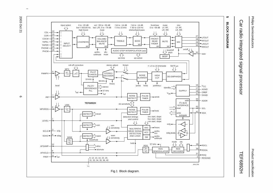
2 GENERAL DESCRIPTION
The TEF6892H is a monolithic BiMOS integrated circuitcomprising the stereo decoder function, weak signalprocessing and ignition noise blanking facility for AM andFM combined with input selector and tone/volume controlfor AM and FM car radio applications. The RDS/RBDSdemodulator function and the RDS/RBDS decoderfunction are included. The device operates with a supplyvoltage of 8 to 9 V.
3 ORDERING INFORMATION
TYPENUMBER
PACKAGE
NAME DESCRIPTION VERSION
TEF6892H QFP44 plastic quad flat package; 44 leads (lead length 1.3 mm);body 10 × 10 × 1.75 mm
SOT307-2

2003 Oct 21 5
Philips Semiconductors Product specification
Car radio integrated signal processor TEF6892H
4 QUICK REFERENCE DATA
SYMBOL PARAMETER CONDITIONS MIN. TYP. MAX. UNIT
VCC supply voltage 8.0 8.5 9.0 V
ICC supply current normal mode − 28 − mA
standby RDS; audio on − 24 − mA
standby audio; RDS on − 19 − mA
standby − 15 − mA
Stereo decoder path
αcs channel separation fFMMPX = 1 kHz 40 − − dB
S/N signal-to-noise ratio fFMMPX = 20 Hz to 15 kHz 75 − − dB
THD total harmonic distortion FM mode; fFMMPX = 1 kHz − − 0.3 %
Tone/volume control
Vi(max)(rms) maximum input voltage level atpins TAPEL, TAPER, CDL, CDR,CDCM, PHONE and PHCM(RMS value)
THD = 0.1%; Gvol = −6 dB 2 − − V
Vi(NAV)(max)(rms) maximum input voltage level atpin NAV (RMS value)
THD = 1%; fNAV = 1 kHz 0.3 − − V
THD total harmonic distortion TAPE and CD inputs;faudio = 20 Hz to 20 kHz;Vi = 1 V (RMS)
− 0.01 0.1 %
Gvol volume/balance gain control maximum setting − 20 − dB
minimum setting − −59 − dB
Gstep(vol) step resolution gain (volume) − 1 − dB
Gloudness loudness gain control floudness(low) = 50 Hz; high boost on
maximum setting; 1 kHz tone − 0 − dB
minimum setting; 1 kHz tone − −20 − dB
Gtreble treble gain control maximum setting − 14 − dB
minimum setting − −14 − dB
Gstep(treble) step resolution gain (treble) − 2 − dB
Gbass bass gain control maximum setting; symmetrical boost − 14 − dB
minimum setting; asymmetrical cut − −14 − dB
Gstep(bass) step resolution gain (bass) − 2 − dB
2003O
ct216
Philips S
emiconductors
Product specification
Car radio integrated signal processor
TE
F6892H
This text is here in white to force landscape pages to be rotated correctly when browsing through the pdf in the Acrobat reader.This text is here in_white to force landscape pages to be rotated correctly when browsing through the pdf in the Acrobat reader.This text is here inThis text is here inwhite to force landscape pages to be rotated correctly when browsing through the pdf in the Acrobat reader. white to force landscape pages to be ...
5B
LOC
K D
IAG
RA
M
hand
book
, ful
l pag
ewid
th
NOISEDETECT
NOISEBLANKER
PILOTCANCEL
INPUTSELECT25
26
5
23
24
21
20
22CDL
CDR
CDCM
TAPEL
TAPER
PHONE
PHCM
FMMPX
7AM
6MPXRDS
1LEVEL
3
4
SCLG
SDAG
10
i.c.
8, 12, 13, 14, 15, 19,31, 33, 34, 35, 36, 40
AFSAMP
9AFHOLD 37
38
39
2RDSGND
MHC356
RDQ
RDDA
RDCL
42SDA
43SCL
++
+++
++
−
−
PILOT/REFERENCE
PLL
STEREODECODER HIGH
CUT
f: 1.5 to 15 kHz/widestereo adjustroll-off correction fm/am
NOISEDETECT
nb sensitivity
usnsensitivity
level
detection timingsand control
usn
sclg
11FREF fref
sdag
USN
MPX
snc start, slopehcc start, slopesm start, slope
MULTIPATH/WEAK SIGNALDETECTIONAND LOGIC
SNC
HCC
DETECT
SM
hold
RDSDEMODULATOR
57 kHz
sclg
mode rds
writeautogate
I2C-BUSINTERFACE
SUPPLY
read
addr
sdag
RDS
RDSDECODER
PULSETIMER
TEF6892H
PULSETIMER
amnb
amnbfmsnc
amfm-softmute
afu-mute
asiasi
asi time asi active
level/offpitch
on/off
asi
fmnb amfmhcc
fmnb
fmsnc
amfm-hcc
wamsensitivity
amfm-softmute
LOUDNESS
input select 0 to −20 dBlow f: 50/100 Hz
high boost
DE-EMPHASIS
50/75 µs
Vref
standby
44ADDR
41DGND
18CREF
17 AGND
16 VCC
32NAV
30RROUT
29LROUT
28RFOUT
27LFOUT
DETECT
wamWAM
afus
reset/hold
afumute
Ireffref
TREBLE
AUDIO STEP INTERPOLATION (asi)
BEEP
+14 to −14 dBf: 8 to 15 kHz
+14 to −14 dBf: 60 to 120 Hz
shelve/band-pass
BASS
asi asi
front/rear0 to −59 dB
FRONT/REAR
FADER
mute:LF, RF,LR, RR
mix:LF, RF,LR, RR
MUTE MIX
VOLUME/BALANCE/
MUTE
vol: +20 to −59 dBbal: L/R, 0 to −79 dB
mute
57 kHz
38 kHz19 kHz
stereo
DETECT
level
Fig.1 Block diagram.
2003 Oct 21 7
Philips Semiconductors Product specification
Car radio integrated signal processor TEF6892H
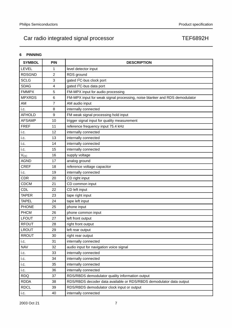
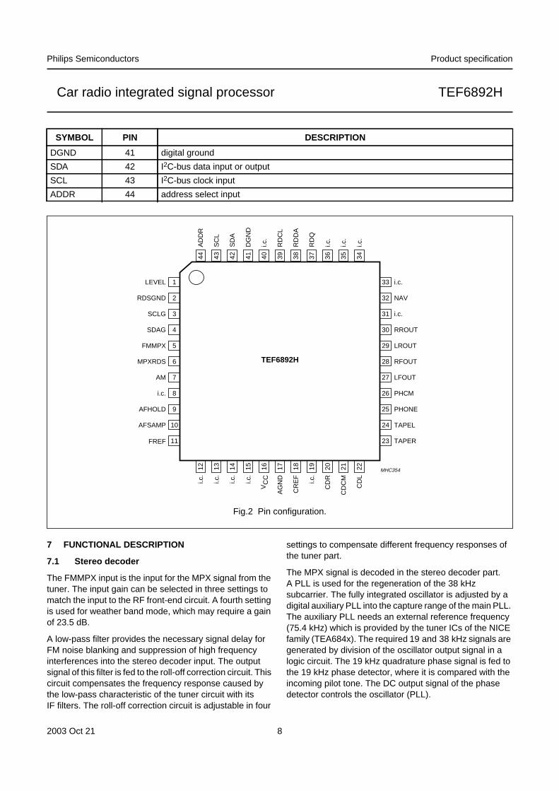
6 PINNING
SYMBOL PIN DESCRIPTION
LEVEL 1 level detector input
RDSGND 2 RDS ground
SCLG 3 gated I2C-bus clock port
SDAG 4 gated I2C-bus data port
FMMPX 5 FM-MPX input for audio processing
MPXRDS 6 FM-MPX input for weak signal processing, noise blanker and RDS demodulator
AM 7 AM audio input
i.c. 8 internally connected
AFHOLD 9 FM weak signal processing hold input
AFSAMP 10 trigger signal input for quality measurement
FREF 11 reference frequency input 75.4 kHz
i.c. 12 internally connected
i.c. 13 internally connected
i.c. 14 internally connected
i.c. 15 internally connected
VCC 16 supply voltage
AGND 17 analog ground
CREF 18 reference voltage capacitor
i.c. 19 internally connected
CDR 20 CD right input
CDCM 21 CD common input
CDL 22 CD left input
TAPER 23 tape right input
TAPEL 24 tape left input
PHONE 25 phone input
PHCM 26 phone common input
LFOUT 27 left front output
RFOUT 28 right front output
LROUT 29 left rear output
RROUT 30 right rear output
i.c. 31 internally connected
NAV 32 audio input for navigation voice signal
i.c. 33 internally connected
i.c. 34 internally connected
i.c. 35 internally connected
i.c. 36 internally connected
RDQ 37 RDS/RBDS demodulator quality information output
RDDA 38 RDS/RBDS decoder data available or RDS/RBDS demodulator data output
RDCL 39 RDS/RBDS demodulator clock input or output
i.c. 40 internally connected
2003 Oct 21 8
Philips Semiconductors Product specification
Car radio integrated signal processor TEF6892H
DGND 41 digital ground
SDA 42 I2C-bus data input or output
SCL 43 I2C-bus clock input
ADDR 44 address select input
SYMBOL PIN DESCRIPTION
handbook, full pagewidth
TEF6892H
MHC354
1
2
3
4
5
6
7
8
9
10
11
33
32
31
30
29
28
27
26
25
24
23
12 13 14 15 16 17 18 19 20 21 22
44 43 42 41 40 39 38 37 36 35 34
AD
DR
SC
L
SD
A
DG
ND
i.c.
RD
CL
RD
DA
RD
Q
i.c.
i.c.
i.c.
i.c.
i.c.
i.c.
i.c.
VC
C
AG
ND
CR
EF
i.c.
CD
R
CD
CM
CD
L
LEVEL
RDSGND
SCLG
SDAG
FMMPX
MPXRDS
AM
i.c.
AFHOLD
AFSAMP
FREF
i.c.
NAV
i.c.
RROUT
LROUT
RFOUT
LFOUT
PHCM
PHONE
TAPEL
TAPER
Fig.2 Pin configuration.
7 FUNCTIONAL DESCRIPTION
7.1 Stereo decoder
The FMMPX input is the input for the MPX signal from thetuner. The input gain can be selected in three settings tomatch the input to the RF front-end circuit. A fourth settingis used for weather band mode, which may require a gainof 23.5 dB.
A low-pass filter provides the necessary signal delay forFM noise blanking and suppression of high frequencyinterferences into the stereo decoder input. The outputsignal of this filter is fed to the roll-off correction circuit. Thiscircuit compensates the frequency response caused bythe low-pass characteristic of the tuner circuit with itsIF filters. The roll-off correction circuit is adjustable in four
settings to compensate different frequency responses ofthe tuner part.
The MPX signal is decoded in the stereo decoder part.A PLL is used for the regeneration of the 38 kHzsubcarrier. The fully integrated oscillator is adjusted by adigital auxiliary PLL into the capture range of the main PLL.The auxiliary PLL needs an external reference frequency(75.4 kHz) which is provided by the tuner ICs of the NICEfamily (TEA684x). The required 19 and 38 kHz signals aregenerated by division of the oscillator output signal in alogic circuit. The 19 kHz quadrature phase signal is fed tothe 19 kHz phase detector, where it is compared with theincoming pilot tone. The DC output signal of the phasedetector controls the oscillator (PLL).

2003 Oct 21 9
Philips Semiconductors Product specification
Car radio integrated signal processor TEF6892H
The pilot detector is driven by an internally generatedin-phase 19 kHz signal. Its pilot dependent voltageactivates the stereo indicator bit and sets the stereodecoder to stereo mode. The same voltage is used tocontrol the amplitude of an anti-phase internally generated19 kHz signal. In the pilot canceller, the pilot tone iscompensated by this anti-phase 19 kHz signal.
The signal is then decoded in the decoder part. The sidesignal is demodulated and combined with the main signalto the left and right audio channels. A fine adjustment ofthe roll-off compensation is done by adjusting the gain ofthe L-R signal in 16 steps. A smooth mono to stereotakeover is achieved by controlling the efficiency of thematrix by the FMSNC signal from the weak signalprocessing block.
7.2 FM and AM noise blanker
The FM/AM switch selects the output signal of the stereodecoder (FM mode) or the signal from the AM input for thenoise blanker block. In FM mode the noise blankeroperates as a sample and hold circuit, while in AM mode itmutes the audio signal during the interference pulse. Theblanking pulse which triggers the noise blanker isgenerated in the noise detector block.
7.3 High cut control and de-emphasis
The High Cut Control (HCC) part is a low-pass filter circuitwith eight different static roll-off response curves. Thecut-off frequencies of these filter curves can be selected byI2C-bus to match different application requirements. TheHCC circuit also provides a dynamic control of the filterresponse. This function is controlled by the AMFMHCCsignal from the weak signal processing.
The signal passes the de-emphasis block with twode-emphasis values (50 and 75 µs), which can be selectedvia I2C-bus, and is fed to the input selector.
7.4 Noise detector
7.4.1 FM NOISE DETECTOR
The trigger signal for the FM noise detector is derived fromthe MPXRDS input signal and the LEVEL signal. In theMPXRDS path a four pole high-pass filter (100 kHz)separates the noise spikes from the wanted MPX signal.Another detector circuit triggers on noise spikes on thelevel voltage. The signals of both detectors are combinedto achieve a reliable trigger signal for the noise blanker.AGC circuits in the detector part control the gaindepending on the average noise in the signals to preventfalse triggering. The sensitivity of the triggering from the
MPXRDS signal can be adjusted in four steps, thetriggering from the LEVEL signal in three steps.
7.4.2 AM NOISE DETECTOR
The trigger pulse for the AM noise blanker is derived fromthe AM audio signal. The noise spikes are detected by aslew rate detector, which detects excessive slew rateswhich do not occur in normal audio signals. The sensitivityof the AM noise blanker can be adjusted in four steps.
7.5 Multipath/weak signal processing
The multipath (MPH)/weak signal processing blockdetects quality degradations in the incoming FM signal andcontrols the processing of the audio signal accordingly.There are three different quality criteria:
• The average value of the level voltage
• The AM components on the level voltage[Wideband AM (WAM)]
• The high frequency components in the MPX signal[Ultrasonic Noise (USN)].
The level voltage is converted to a digital value by an 8-bitanalog-to-digital converter. A digital filter circuit (WAMfilter) derives the wideband AM components from the levelsignal. The high frequency components in the MPX signalsare measured with an analog-to-digital converter (USNADC) at the output of the 100 kHz high-pass filter in theMPXRDS path.
The values of these three signals are externally availablevia the I2C-bus.
In the weak signal processing block the three digitalsignals are combined in a specific way and used for thegeneration of control signals for soft mute, stereo blend(stereo noise control, FMSNC) and high cut control(AMFMHCC).
The sensitivities of the detector circuits (WAM and USN)are adjustable via the I2C-bus.
Also the start values and the slopes of the control functionssoft mute, stereo blend and high cut control can be set viathe I2C-bus.
Soft mute, stereo blend and HCC are set on hold duringthe AF updating (quality check of alternative frequency) toavoid an influence of the tuning procedure on the weaksignal processing conditions.
In AM mode the soft mute and high cut control areavailable too, the weak signal block is controlled by theaverage value of the level voltage.

2003 Oct 21 10
Philips Semiconductors Product specification
Car radio integrated signal processor TEF6892H
7.6 Tone/volume control
The tone/volume control part consists of the followingstages:
• Input selector
• Loudness control
• Volume/balance control with muting
• Treble control
• Bass control
• Fader and output mute
• Beep generator
• NAV input
• Output mixer.
The settings of all stages are controlled via the I2C-bus.
The stages input selector, loudness, volume/balance,bass, and fader/output mute include the Audio StepInterpolation (ASI) function. This minimizes pops bysmoothing the transitions in the audio signal during theswitching of the controls. The transition time of the ASIfunction is programmable by I2C-bus in four steps.
7.6.1 INPUT SELECTOR
The input selector selects one of four input sources:
• Two external stereo inputs (CD and TAPE)
• One external mono input (PHONE)
• One internal stereo input (AM/FM).
7.6.2 LOUDNESS
The output of the input selector is fed into the loudnesscircuit. Four different loudness curves can be selected viathe I2C-bus. The control range is between 0 and −20 dBwith a step size of 1 dB; see Figs 16 to 19.
7.6.3 VOLUME/BALANCE
The volume/balance control is used for volume setting andalso for balance adjustment. The control range of thevolume/balance control is between +20 and −59 dB insteps of 1 dB.
The combination of loudness and volume/balance realizesan overall control range of +20 to −79 dB.
7.6.4 TREBLE
The signal is then fed to the treble control stage. Thecontrol range is between +14 and −14 dB in steps of 2 dB.Figure 20 shows the control characteristic. Four differentfilter frequencies can be selected.
7.6.5 BASS
The characteristic of the bass attenuation curves can beset to shelve or band-pass. Four different frequencies canbe selected as centre frequency of the band-pass curve.Figures 21 and 22 show the bass curves with a band-passfilter frequency of 60 Hz. The control range is between+14 and −14 dB in steps of 2 dB.
7.6.6 FADER/MUTE
The four fader/mute blocks are located at the end of thetone/volume chain. The control range of these attenuatorsis 0 to −59 dB. The step size is:
• 1 dB between 0 and −15 dB
• 2.5 dB between −15 and −45 dB
• 3 dB between −45 and −51 dB
• 4 dB between −51 and −59 dB.
7.6.7 BEEP GENERATOR AND NAV INPUT WITH OUTPUT
MIXER
The output mixer circuit can add an additional audio signalto any of the four outputs together with the main signal orinstead of the main signal.
The additional signal can be generated internally by thebeep generator with four different audio frequencies orapplied to the NAV input, for instance a navigation voicesignal.
7.7 RDS demodulator and decoder
7.7.1 RDS DEMODULATOR
The RDS demodulator recovers and regenerates thecontinuously transmitted RDS or RBDS data stream of themultiplex signal (MPXRDS) and provides the signals clock(RDCL), data (RDDA) and quality (RDQ) for external useor further processing by the integrated RDS decoder. TheRDS demodulator uses the reference frequency(75.4 kHz) from the tuner IC and does not need a crystal.
7.7.2 RDS DECODER
The RDS decoder provides block synchronization, errorcorrection and flywheel function for reliable extraction ofRDS or RBDS block data. Different modes of operationcan be selected to fit different application requirements.Availability of new data is signalled by read bit RDAV andoutput pin RDDA. Up to two blocks of data and statusinformation are available via the I2C-bus in a singletransmission.
2003 Oct 21 11
Philips Semiconductors Product specification
Car radio integrated signal processor TEF6892H
8 LIMITING VALUESIn accordance with the Absolute Maximum Rating System (IEC 60134).
Notes
1. Machine model (R = 0 Ω, C = 200 pF).
2. Human body model (R = 1.5 kΩ, C = 100 pF).
9 THERMAL CHARACTERISTICS
10 CHARACTERISTICSFM part: fFMMPX = 1 kHz at VFMMPX = 767 mV (RMS); pilot off (100% FM). AM part: fAM = 1 kHz atVAM = 967 mV (RMS) (100% AM). Treble: 10 kHz filter frequency. Bass: 60 Hz filter frequency. Loudness: 50 Hz filterfrequency; treble loudness on. VCC = 8.5 V; Tamb = 25 °C; see Fig.23; unless otherwise specified.
SYMBOL PARAMETER CONDITIONS MIN. MAX. UNIT
VCC supply voltage −0.3 +10 V
Vi input voltage for any pin −0.3 VCC + 0.3 V
Tstg storage temperature −65 +150 °CTamb ambient temperature −40 +85 °CVesd electrostatic discharge voltage note 1 −200 +200 V
note 2 −2000 +2000 V
SYMBOL PARAMETER CONDITIONS VALUE UNIT
Rth(j-a) thermal resistance from junction to ambient in free air 61 K/W
SYMBOL PARAMETER CONDITIONS MIN. TYP. MAX. UNIT
VCC supply voltage 8.0 8.5 9.0 V
ICC supply current normal mode − 28 − mA
standby RDS; audio on − 24 − mA
standby audio; RDS on − 19 − mA
standby − 15 − mA
Logic pins
VIH HIGH-level input voltage pins SDA, SCL, ADDR, SDAG andRDCL
1.75 − 5.5 V
pins AFHOLD and AFSAMP 1.75 − 5.5 V
VIL LOW-level input voltage pins SDA, SCL, ADDR, SDAG andRDCL
−0.2 − +1.0 V
pins AFHOLD and AFSAMP −0.2 − +1.0 V
VOH HIGH-level output voltage pins RDCL and RDDA; IOH = 2.5 µA 2.6 − − V
VOL LOW-level output voltage pins SCLG, RDCL and RDDA;IOL = 3 mA; note 1
− − 0.4 V
pin SDA; IOL = 3 mA − − 0.4 V
2003 Oct 21 12
Philips Semiconductors Product specification
Car radio integrated signal processor TEF6892H
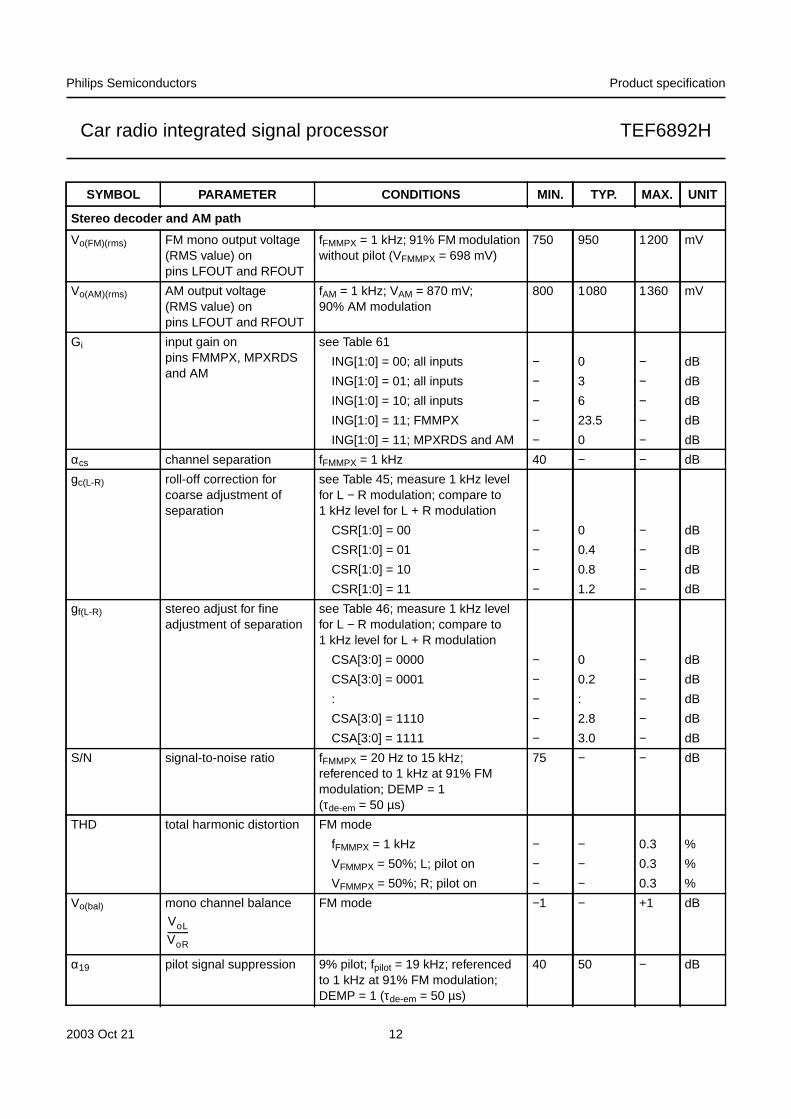
Stereo decoder and AM path
Vo(FM)(rms) FM mono output voltage(RMS value) onpins LFOUT and RFOUT
fFMMPX = 1 kHz; 91% FM modulationwithout pilot (VFMMPX = 698 mV)
750 950 1200 mV
Vo(AM)(rms) AM output voltage(RMS value) onpins LFOUT and RFOUT
fAM = 1 kHz; VAM = 870 mV;90% AM modulation
800 1080 1360 mV
Gi input gain onpins FMMPX, MPXRDSand AM
see Table 61
ING[1:0] = 00; all inputs − 0 − dB
ING[1:0] = 01; all inputs − 3 − dB
ING[1:0] = 10; all inputs − 6 − dB
ING[1:0] = 11; FMMPX − 23.5 − dB
ING[1:0] = 11; MPXRDS and AM − 0 − dB
αcs channel separation fFMMPX = 1 kHz 40 − − dB
gc(L-R) roll-off correction forcoarse adjustment ofseparation
see Table 45; measure 1 kHz levelfor L − R modulation; compare to1 kHz level for L + R modulation
CSR[1:0] = 00 − 0 − dB
CSR[1:0] = 01 − 0.4 − dB
CSR[1:0] = 10 − 0.8 − dB
CSR[1:0] = 11 − 1.2 − dB
gf(L-R) stereo adjust for fineadjustment of separation
see Table 46; measure 1 kHz levelfor L − R modulation; compare to1 kHz level for L + R modulation
CSA[3:0] = 0000 − 0 − dB
CSA[3:0] = 0001 − 0.2 − dB
: − : − dB
CSA[3:0] = 1110 − 2.8 − dB
CSA[3:0] = 1111 − 3.0 − dB
S/N signal-to-noise ratio fFMMPX = 20 Hz to 15 kHz;referenced to 1 kHz at 91% FMmodulation; DEMP = 1(τde-em = 50 µs)
75 − − dB
THD total harmonic distortion FM mode
fFMMPX = 1 kHz − − 0.3 %
VFMMPX = 50%; L; pilot on − − 0.3 %
VFMMPX = 50%; R; pilot on − − 0.3 %
Vo(bal) mono channel balance FM mode −1 − +1 dB
α19 pilot signal suppression 9% pilot; fpilot = 19 kHz; referencedto 1 kHz at 91% FM modulation;DEMP = 1 (τde-em = 50 µs)
40 50 − dB
SYMBOL PARAMETER CONDITIONS MIN. TYP. MAX. UNIT
VoL
VoR----------
2003 Oct 21 13
Philips Semiconductors Product specification
Car radio integrated signal processor TEF6892H
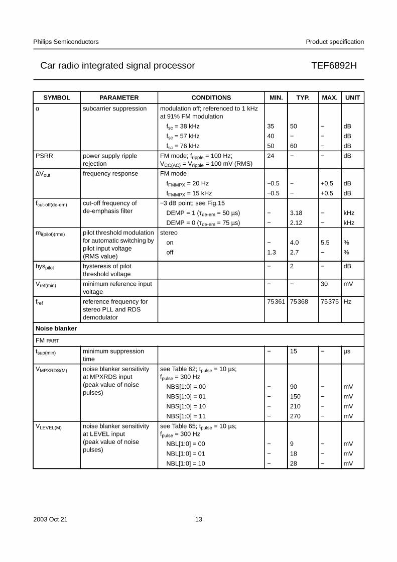
α subcarrier suppression modulation off; referenced to 1 kHzat 91% FM modulation
fsc = 38 kHz 35 50 − dB
fsc = 57 kHz 40 − − dB
fsc = 76 kHz 50 60 − dB
PSRR power supply ripplerejection
FM mode; fripple = 100 Hz;VCC(AC) = Vripple = 100 mV (RMS)
24 − − dB
∆Vout frequency response FM mode
fFMMPX = 20 Hz −0.5 − +0.5 dB
fFMMPX = 15 kHz −0.5 − +0.5 dB
fcut-off(de-em) cut-off frequency ofde-emphasis filter
−3 dB point; see Fig.15
DEMP = 1 (τde-em = 50 µs) − 3.18 − kHz
DEMP = 0 (τde-em = 75 µs) − 2.12 − kHz
mi(pilot)(rms) pilot threshold modulationfor automatic switching bypilot input voltage(RMS value)
stereo
on − 4.0 5.5 %
off 1.3 2.7 − %
hyspilot hysteresis of pilotthreshold voltage
− 2 − dB
Vref(min) minimum reference inputvoltage
− − 30 mV
fref reference frequency forstereo PLL and RDSdemodulator
75361 75368 75375 Hz
Noise blanker
FM PART
tsup(min) minimum suppressiontime
− 15 − µs
VMPXRDS(M) noise blanker sensitivityat MPXRDS input(peak value of noisepulses)
see Table 62; tpulse = 10 µs;fpulse = 300 Hz
NBS[1:0] = 00 − 90 − mV
NBS[1:0] = 01 − 150 − mV
NBS[1:0] = 10 − 210 − mV
NBS[1:0] = 11 − 270 − mV
VLEVEL(M) noise blanker sensitivityat LEVEL input(peak value of noisepulses)
see Table 65; tpulse = 10 µs;fpulse = 300 Hz
NBL[1:0] = 00 − 9 − mV
NBL[1:0] = 01 − 18 − mV
NBL[1:0] = 10 − 28 − mV
SYMBOL PARAMETER CONDITIONS MIN. TYP. MAX. UNIT

2003 Oct 21 14
Philips Semiconductors Product specification
Car radio integrated signal processor TEF6892H
AM PART
tsup(min) minimum suppressiontime
− 200 − µs
MAM noise blanker sensitivity see Table 62; faudio = 2 kHz
NBS[1:0] = 00 − 110 − %
NBS[1:0] = 01 − 140 − %
NBS[1:0] = 10 − 175 − %
NBS[1:0] = 11 − 220 − %
Weak signal processing
DETECTORS
Veq(USN) USN sensitivity equivalentlevel voltage
see Fig.5; fMPXRDS = 150 kHz;VMPXRDS = 250 mV (RMS);HCMP = 1; note 2
USS[1:0] = 00 − 2.5 − V
USS[1:0] = 01 − 2 − V
USS[1:0] = 10 − 1.5 − V
USS[1:0] = 11 − 0.5 − V
Veq(WAM) WAM sensitivityequivalent level voltage
see Fig.6; VLEVEL = 200 mV (p-p) atf = 21 kHz on the level voltage;HCMP = 1; note 2
WAS[1:0] = 00 − 2.5 − V
WAS[1:0] = 01 − 2 − V
WAS[1:0] = 10 − 1.5 − V
WAS[1:0] = 11 − 0.5 − V
tLEVEL(attack) level detector attack time(soft mute and HCC)
see Table 49; LETF = 0; SEAR = 0
LET[1:0] = 00 − 3 − s
LET[1:0] = 01 − 3 − s
LET[1:0] = 10 − 1.5 − s
LET[1:0] = 11 − 0.5 − s
see Table 49; LETF = 1; SEAR = 0
LET[1:0] = 00 − 0.5 − s
LET[1:0] = 01 − 0.17 − s
LET[1:0] = 10 − 0.06 − s
LET[1:0] = 11 − 0.06 − s
search mode; SEAR = 1 − 60 − ms
SYMBOL PARAMETER CONDITIONS MIN. TYP. MAX. UNIT

2003 Oct 21 15
Philips Semiconductors Product specification
Car radio integrated signal processor TEF6892H
tLEVEL(decay) level detector decay time(soft mute and HCC)
see Table 49; LETF = 0; SEAR = 0
LET[1:0] = 00 − 3 − s
LET[1:0] = 01 − 6 − s
LET[1:0] = 10 − 1.5 − s
LET[1:0] = 11 − 1.5 − s
see Table 49; LETF = 1; SEAR = 0
LET[1:0] = 00 − 0.5 − s
LET[1:0] = 01 − 0.5 − s
LET[1:0] = 10 − 0.17 − s
LET[1:0] = 11 − 0.06 − s
search mode; SEAR = 1 − 60 − ms
tMPH(attack) multipath detector attacktime (SNC)
see Table 50; SEAR = 0
MPT[1:0] = 00 − 0.5 − s
MPT[1:0] = 01 − 0.5 − s
MPT[1:0] = 10 − 0.5 − s
MPT[1:0] = 11 − 0.25 − s
search mode; SEAR = 1 − 60 − ms
tMPH(decay) multipath detector decaytime (SNC)
see Table 50; SEAR = 0
MPT[1:0] = 00 − 12 − s
MPT[1:0] = 01 − 24 − s
MPT[1:0] = 10 − 6 − s
MPT[1:0] = 11 − 6 − s
search mode; SEAR = 1 − 60 − ms
tUSN(attack) USN detector attack time(soft mute and SNC)
− 1 − ms
tUSN(decay) USN detector decay time(soft mute and SNC)
− 1 − ms
∆USS USN detectordesensitization
USN sensitivity setting (USS) versuslevel voltage (USN sensitivity settingis automatically reduced as levelvoltage decreases)
VLEVEL > 1.25 V − − 3 −1.25 V > VLEVEL > 1.125 V − − 2 −1.125 V > VLEVEL > 1.0 V − − 1 −1.0 V > VLEVEL − − 0 −
tWAM(attack) WAM detector attack time(SNC)
− 1 − ms
tWAM(decay) WAM detector decay time(SNC)
− 1 − ms
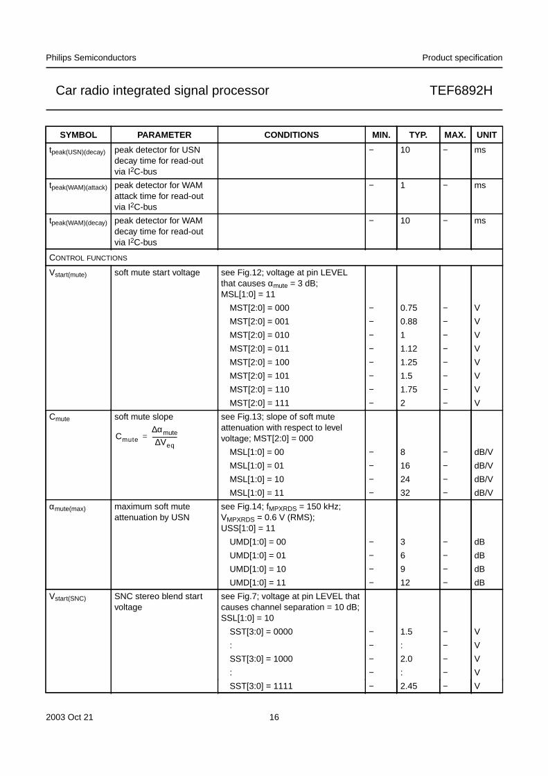
tpeak(USN)(attack) peak detector for USNattack time for read-outvia I2C-bus
− 1 − ms
SYMBOL PARAMETER CONDITIONS MIN. TYP. MAX. UNIT
2003 Oct 21 16
Philips Semiconductors Product specification
Car radio integrated signal processor TEF6892H
tpeak(USN)(decay) peak detector for USNdecay time for read-outvia I2C-bus
− 10 − ms
tpeak(WAM)(attack) peak detector for WAMattack time for read-outvia I2C-bus
− 1 − ms
tpeak(WAM)(decay) peak detector for WAMdecay time for read-outvia I2C-bus
− 10 − ms
CONTROL FUNCTIONS
Vstart(mute) soft mute start voltage see Fig.12; voltage at pin LEVELthat causes αmute = 3 dB;MSL[1:0] = 11
MST[2:0] = 000 − 0.75 − V
MST[2:0] = 001 − 0.88 − V
MST[2:0] = 010 − 1 − V
MST[2:0] = 011 − 1.12 − V
MST[2:0] = 100 − 1.25 − V
MST[2:0] = 101 − 1.5 − V
MST[2:0] = 110 − 1.75 − V
MST[2:0] = 111 − 2 − V
Cmute soft mute slope see Fig.13; slope of soft muteattenuation with respect to levelvoltage; MST[2:0] = 000
MSL[1:0] = 00 − 8 − dB/V
MSL[1:0] = 01 − 16 − dB/V
MSL[1:0] = 10 − 24 − dB/V
MSL[1:0] = 11 − 32 − dB/V
αmute(max) maximum soft muteattenuation by USN
see Fig.14; fMPXRDS = 150 kHz;VMPXRDS = 0.6 V (RMS);USS[1:0] = 11
UMD[1:0] = 00 − 3 − dB
UMD[1:0] = 01 − 6 − dB
UMD[1:0] = 10 − 9 − dB
UMD[1:0] = 11 − 12 − dB
Vstart(SNC) SNC stereo blend startvoltage
see Fig.7; voltage at pin LEVEL thatcauses channel separation = 10 dB;SSL[1:0] = 10
SST[3:0] = 0000 − 1.5 − V
: − : − V
SST[3:0] = 1000 − 2.0 − V
: − : − V
SST[3:0] = 1111 − 2.45 − V
SYMBOL PARAMETER CONDITIONS MIN. TYP. MAX. UNIT
Cmute
αmute∆Veq∆-----------------
=
2003 Oct 21 17
Philips Semiconductors Product specification
Car radio integrated signal processor TEF6892H
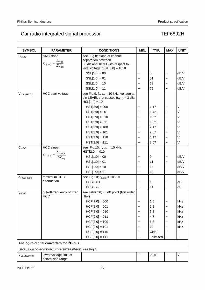
CSNC SNC slope see Fig.8; slope of channelseparation between30 dB and 10 dB with respect tolevel voltage; SST[3:0] = 1010
SSL[1:0] = 00 − 38 − dB/V
SSL[1:0] = 01 − 51 − dB/V
SSL[1:0] = 10 − 63 − dB/V
SSL[1:0] = 11 − 72 − dB/V
Vstart(HCC) HCC start voltage see Fig.9; faudio = 10 kHz; voltage atpin LEVEL that causes αHCC = 3 dB;HSL[1:0] = 10
HST[2:0] = 000 − 1.17 − V
HST[2:0] = 001 − 1.42 − V
HST[2:0] = 010 − 1.67 − V
HST[2:0] = 011 − 1.92 − V
HST[2:0] = 100 − 2.17 − V
HST[2:0] = 101 − 2.67 − V
HST[2:0] = 110 − 3.17 − V
HST[2:0] = 111 − 3.67 − V
CHCC HCC slope see Fig.10; faudio = 10 kHz;HST[2:0] = 010
HSL[1:0] = 00 − 9 − dB/V
HSL[1:0] = 01 − 11 − dB/V
HSL[1:0] = 10 − 14 − dB/V
HSL[1:0] = 11 − 18 − dB/V
αHCC(max) maximum HCCattenuation
see Fig.10; faudio = 10 kHz
HCSF = 1 − 10 − dB
HCSF = 0 − 14 − dB
fcut-off cut-off frequency of fixedHCC
see Table 56; −3 dB point (first orderfilter)
HCF[2:0] = 000 − 1.5 − kHz
HCF[2:0] = 001 − 2.2 − kHz
HCF[2:0] = 010 − 3.3 − kHz
HCF[2:0] = 011 − 4.7 − kHz
HCF[2:0] = 100 − 6.8 − kHz
HCF[2:0] = 101 − 10 − kHz
HCF[2:0] = 110 − wide − −HCF[2:0] = 111 − unlimited − −
Analog-to-digital converters for I 2C-bus
LEVEL ANALOG-TO-DIGITAL CONVERTER (8-BIT); see Fig.4
VLEVEL(min) lower voltage limit ofconversion range
− 0.25 − V
SYMBOL PARAMETER CONDITIONS MIN. TYP. MAX. UNIT
CSNC
αcs∆Veq∆-------------
=
CHCC
αHCC∆Veq∆-----------------
=
2003 Oct 21 18
Philips Semiconductors Product specification
Car radio integrated signal processor TEF6892H
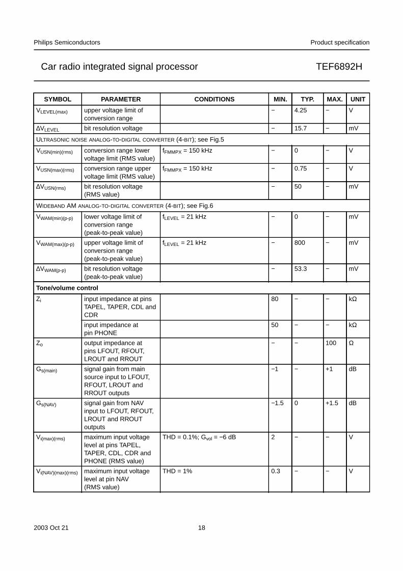
VLEVEL(max) upper voltage limit ofconversion range
− 4.25 − V
∆VLEVEL bit resolution voltage − 15.7 − mV
ULTRASONIC NOISE ANALOG-TO-DIGITAL CONVERTER (4-BIT); see Fig.5
VUSN(min)(rms) conversion range lowervoltage limit (RMS value)
fFMMPX = 150 kHz − 0 − V
VUSN(max)(rms) conversion range uppervoltage limit (RMS value)
fFMMPX = 150 kHz − 0.75 − V
∆VUSN(rms) bit resolution voltage(RMS value)
− 50 − mV
WIDEBAND AM ANALOG-TO-DIGITAL CONVERTER (4-BIT); see Fig.6
VWAM(min)(p-p) lower voltage limit ofconversion range(peak-to-peak value)
fLEVEL = 21 kHz − 0 − mV
VWAM(max)(p-p) upper voltage limit ofconversion range(peak-to-peak value)
fLEVEL = 21 kHz − 800 − mV
∆VWAM(p-p) bit resolution voltage(peak-to-peak value)
− 53.3 − mV
Tone/volume control
Zi input impedance at pinsTAPEL, TAPER, CDL andCDR
80 − − kΩ
input impedance atpin PHONE
50 − − kΩ
Zo output impedance atpins LFOUT, RFOUT,LROUT and RROUT
− − 100 Ω
Gs(main) signal gain from mainsource input to LFOUT,RFOUT, LROUT andRROUT outputs
−1 − +1 dB
Gs(NAV) signal gain from NAVinput to LFOUT, RFOUT,LROUT and RROUToutputs
−1.5 0 +1.5 dB
Vi(max)(rms) maximum input voltagelevel at pins TAPEL,TAPER, CDL, CDR andPHONE (RMS value)
THD = 0.1%; Gvol = −6 dB 2 − − V
Vi(NAV)(max)(rms) maximum input voltagelevel at pin NAV(RMS value)
THD = 1% 0.3 − − V
SYMBOL PARAMETER CONDITIONS MIN. TYP. MAX. UNIT

2003 Oct 21 19
Philips Semiconductors Product specification
Car radio integrated signal processor TEF6892H
Vo(max)(rms) maximum output voltage(RMS value)
THD = 0.1%; Gvol = +6 dB 2 − − V
worst case load: RL = 2 kΩ,CL = 10 nF, THD = 1%
2 − − V
fmax frequency response(pins TAPER, TAPEL,CDR and CDL)
upper −0.5 dB point; referencedto 1 kHz
20 − − kHz
CMRR common mode rejectionratio
faudio = 20 Hz to 20 kHz on CD andPHONE inputs
Gvol = 0 dB 40 − − dB
Gvol = −15 dB 55 − − dB
αcs channel separation faudio = 20 Hz to 20 kHz 60 80 − dB
αS input isolation of oneselected source to anyother input
faudio = 1 kHz 90 105 − dB
faudio = 20 Hz to 10 kHz 75 90 − dB
faudio = 20 kHz 70 − − dB
THD total harmonic distortion TAPE and CD inputs
faudio = 20 Hz to 10 kHz;Vi = 1 V (RMS)
− 0.01 0.1 %
faudio = 1 kHz; Vi = 2 V (RMS);Gvol = 0 dB
− 0.02 0.1 %
faudio = 20 Hz to 10 kHz;Vi = 2 V (RMS); Gvol = −10 dB
− 0.02 0.2 %
faudio = 25 Hz;Vi = 500 mV (RMS);Gbass = +8 dB; Gvol = 0 dB
− 0.05 0.2 %
faudio = 4 kHz; Vi = 500 mV (RMS);Gtreble = +8 dB; Gvol = 0 dB
− 0.01 0.2 %
NAV input; faudio = 1 kHz;Vo = 300 mV (RMS)
− − 1 %
Vnoise(rms) noise voltage(RMS value)
CCIR-ARM weighted and 20 kHz‘brick wall’ without input signal andshorted AF inputs
Gvol = 0 dB − 12 20 µV
Gbass = +6 dB; Gtreble = +6 dB;Gvol = 0 dB
− 24 35 µV
Gvol = 20 dB; TAPE input (stereo) − 71 100 µV
Gvol = 20 dB; CD input(quasi-differential)
− 100 140 µV
Gvol = −10 dB − 10 18 µV
Gvol = −40 dB; Gloudness = −20 dB − 9.5 13.5 µV
outputs muted − 5 12 µV
using ‘A-weighting’ filter and20 kHz ‘brick wall’; Gvol = −10 dB;Gloudness = −10 dB
− 6.8 10 µV
NAV input − 16 40 µV
SYMBOL PARAMETER CONDITIONS MIN. TYP. MAX. UNIT
2003 Oct 21 20
Philips Semiconductors Product specification
Car radio integrated signal processor TEF6892H
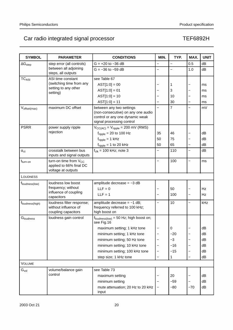
∆Gstep step error (all controls)between all adjoiningsteps, all outputs
G = +20 to −36 dB − − 0.5 dB
G = −36 to −59 dB − − 1.0 dB
TCASI ASI time constant(switching time from anysetting to any othersetting)
see Table 67
AST[1:0] = 00 − 1 − ms
AST[1:0] = 01 − 3 − ms
AST[1:0] = 10 − 10 − ms
AST[1:0] = 11 − 30 − ms
Voffset(max) maximum DC offset between any two settings(non-consecutive) on any one audiocontrol or any one dynamic weaksignal processing control
− 7 − mV
PSRR power supply ripplerejection
VCC(AC) = Vripple = 200 mV (RMS)
fripple = 20 to 100 Hz 35 46 − dB
fripple = 1 kHz 50 75 − dB
fripple = 1 to 20 kHz 50 65 − dB
αct crosstalk between businputs and signal outputs
fclk = 100 kHz; note 3 − 110 − dB
tturn-on turn-on time from VCCapplied to 66% final DCvoltage at outputs
− 100 − ms
LOUDNESS
floudness(low) loudness low boostfrequency; withoutinfluence of couplingcapacitors
amplitude decrease = −3 dB
LLF = 0 − 50 − Hz
LLF = 1 − 100 − Hz
floudness(high) loudness filter response;without influence ofcoupling capacitors
amplitude decrease = −1 dB;frequency referred to 100 kHz;high boost on
− 10 − kHz
Gloudness loudness gain control floudness(low) = 50 Hz; high boost on;see Fig.16
maximum setting; 1 kHz tone − 0 − dB
minimum setting; 1 kHz tone − −20 − dB
minimum setting; 50 Hz tone − −3 − dB
minimum setting; 10 kHz tone − −16 − dB
minimum setting; 100 kHz tone − −15 − dB
step size; 1 kHz tone − 1 − dB
VOLUME
Gvol volume/balance gaincontrol
see Table 73
maximum setting − 20 − dB
minimum setting − −59 − dB
mute attenuation; 20 Hz to 20 kHzinput
− −80 −70 dB
SYMBOL PARAMETER CONDITIONS MIN. TYP. MAX. UNIT

2003 Oct 21 21
Philips Semiconductors Product specification
Car radio integrated signal processor TEF6892H
Gstep(vol) step resolution gain(volume)
see Table 73 − 1 − dB
∆Gset gain set error Gvol = +20 to −36 dB −1 0 +1 dB
Gvol = −36 to −59 dB −3 0 +3 dB
∆Gtrack gain tracking errorbetween left and right
Gvol = +20 to −36 dB − 0 1 dB
Gvol = −36 to −59 dB − 0 3 dB
TREBLE
fcut-off(treble) treble control filter cut-offfrequency
see Table 77; −3 dB frequencyreferred to 100 kHz
TRF[1:0] = 00 − 8 − kHz
TRF[1:0] = 01 − 10 − kHz
TRF[1:0] = 10 − 12 − kHz
TRF[1:0] = 11 − 15 − kHz
Gtreble treble gain control see Table 76
maximum setting − 14 − dB
minimum setting − −14 − dB
Gstep(treble) step resolution gain(treble)
see Table 76 − 2 − dB
BASS
fc(bass) bass control filter centrefrequency
see Table 81
BAF[1:0] = 00 − 60 − Hz
BAF[1:0] = 01 − 80 − Hz
BAF[1:0] = 10 − 100 − Hz
BAF[1:0] = 11 − 120 − Hz
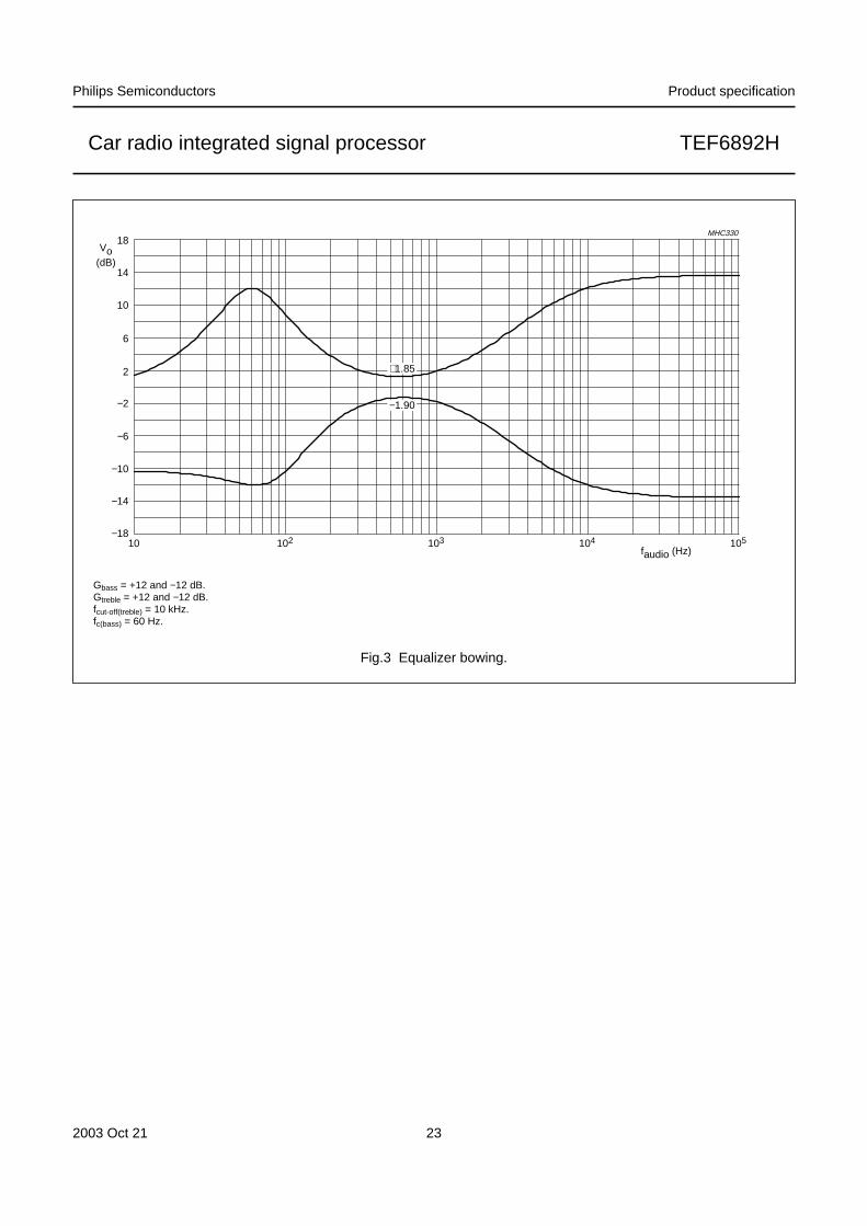
Qbass bass filter quality factor Gbass = +12 dB − 1.0 − −EQbow equalizer bowing faudio = 1 kHz; Vi = 500 mV (RMS);
Gbass = +12 dB; fc(bass) = 60 Hz;Gtreble = +12 dB;fcut-off(treble) = 10 kHz; see Fig.3
− 1.8 − dB
Gbass bass gain control see Table 80
maximum setting; symmetricalboost
− 14 − dB
minimum setting; asymmetrical cut − −14 − dB
minimum setting; symmetrical cut − −14 − dB
Gstep(bass) step resolution gain(bass)
see Table 80 − 2 − dB
FADER
Gfader fader gain control see Table 84
maximum setting − 0 − dB
minimum setting − −59 − dB
mute attenuation; 20 Hz to 20 kHzinput
− −80 −66 dB
SYMBOL PARAMETER CONDITIONS MIN. TYP. MAX. UNIT
2003 Oct 21 22
Philips Semiconductors Product specification
Car radio integrated signal processor TEF6892H
Notes
1. The LOW voltage of pin SCLG is influenced by VSCL: VSCLG(LOW) ≥ VSCL(LOW) + 0.22 V.
2. The equivalent level voltage is that value of the level voltage (at pin LEVEL) which results in the same weak signalcontrol effect (for instance HCC roll-off) as the output value of the specified detector (USN, WAM and MPH).
3. Crosstalk between bus inputs and signal outputs:
Gstep(fader) step resolution gain(fader)
see Table 84
Gfader = 0 to −15 dB − 1 − dB
Gfader = −15 to −45 dB − 2.5 − dB
Gfader = −45 to −51 dB − 3 − dB
Gfader = −51 to −59 dB − 4 − dB
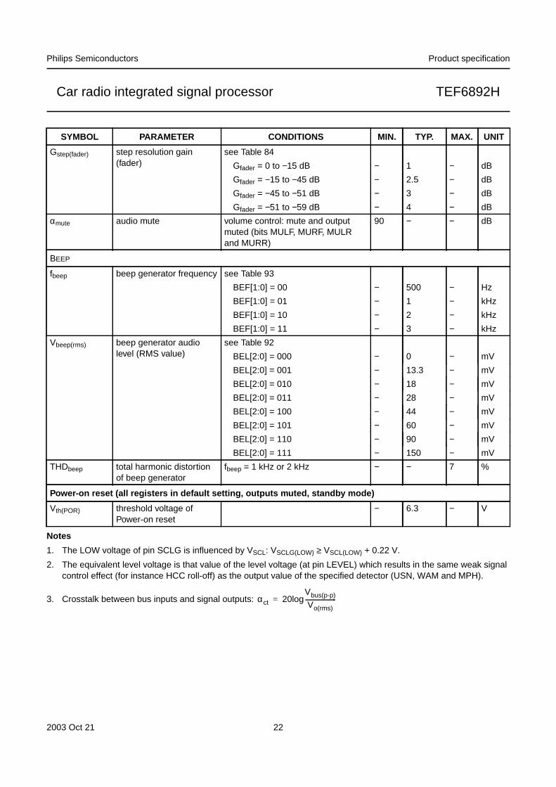
αmute audio mute volume control: mute and outputmuted (bits MULF, MURF, MULRand MURR)
90 − − dB
BEEP
fbeep beep generator frequency see Table 93
BEF[1:0] = 00 − 500 − Hz
BEF[1:0] = 01 − 1 − kHz
BEF[1:0] = 10 − 2 − kHz
BEF[1:0] = 11 − 3 − kHz
Vbeep(rms) beep generator audiolevel (RMS value)
see Table 92
BEL[2:0] = 000 − 0 − mV
BEL[2:0] = 001 − 13.3 − mV
BEL[2:0] = 010 − 18 − mV
BEL[2:0] = 011 − 28 − mV
BEL[2:0] = 100 − 44 − mV
BEL[2:0] = 101 − 60 − mV
BEL[2:0] = 110 − 90 − mV
BEL[2:0] = 111 − 150 − mV
THDbeep total harmonic distortionof beep generator
fbeep = 1 kHz or 2 kHz − − 7 %
Power-on reset (all registers in default setting, outputs muted, standby mode)
Vth(POR) threshold voltage ofPower-on reset
− 6.3 − V
SYMBOL PARAMETER CONDITIONS MIN. TYP. MAX. UNIT
αct 20logVbus(p-p)
Vo(rms)---------------------=
2003 Oct 21 23
Philips Semiconductors Product specification
Car radio integrated signal processor TEF6892H
handbook, full pagewidth
−18
18
14
−10
−14
10
6
2
−2
−6
MHC330
10
Vo(dB)
faudio (Hz)102 103 104 105
+1.85
−1.90
Fig.3 Equalizer bowing.
Gbass = +12 and −12 dB.Gtreble = +12 and −12 dB.fcut-off(treble) = 10 kHz.fc(bass) = 60 Hz.

2003 Oct 21 24
Philips Semiconductors Product specification
Car radio integrated signal processor TEF6892H
11 I2C-BUS PROTOCOL
Table 1 Write mode
Notes
1. S = START condition.
2. A = acknowledge.
3. P = STOP condition.
Table 2 Read mode
Notes
1. S = START condition.
2. A = acknowledge.
3. NA = not acknowledge.
4. P = STOP condition.
Table 3 IC address byte
Table 4 Description of IC address byte
11.1 Read mode
11.1.1 DATA BYTE 1; STATUS
Table 5 Format of data byte 1
S(1) address (write) A(2) subaddress A(2) data byte(s) A(2) P(3)
S(1) address (read) A(2) data byte(s) A(2) data byte NA(3) P(4)
IC ADDRESS MODE
0 0 1 1 0 0 ADDR R/W
BIT SYMBOL DESCRIPTION
7 to 2 − 001100+(ADDR) = IC address.
1 ADDR Address bit. 0 = pin ADDR is grounded; 1 = pin ADDR is floating.
0 R/W Read/Write. 0 = write mode; 1 = read mode.
BIT 7 BIT 6 BIT 5 BIT 4 BIT 3 BIT 2 BIT 1 BIT 0
STIN ASIA AFUS POR RDAV ID2 ID1 ID0
2003 Oct 21 25
Philips Semiconductors Product specification
Car radio integrated signal processor TEF6892H
Table 6 Description of data byte 1
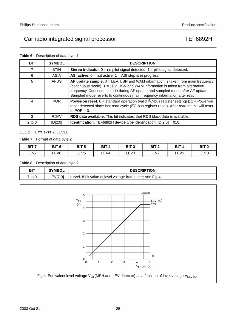
11.1.2 DATA BYTE 2; LEVEL
Table 7 Format of data byte 2
Table 8 Description of data byte 2
BIT SYMBOL DESCRIPTION
7 STIN Stereo indicator. 0 = no pilot signal detected; 1 = pilot signal detected.
6 ASIA ASI active. 0 = not active; 1 = ASI step is in progress.
5 AFUS AF update sample. 0 = LEV, USN and WAM information is taken from main frequency(continuous mode); 1 = LEV, USN and WAM information is taken from alternativefrequency. Continuous mode during AF update and sampled mode after AF update.Sampled mode reverts to continuous main frequency information after read.
4 POR Power-on reset. 0 = standard operation (valid I2C-bus register settings); 1 = Power-onreset detected since last read cycle (I2C-bus register reset). After read the bit will resetto POR = 0.
3 RDAV RDS data available. This bit indicates, that RDS block data is available.
2 to 0 ID[2:0] Identification. TEF6892H device type identification; ID[2:0] = 010.
BIT 7 BIT 6 BIT 5 BIT 4 BIT 3 BIT 2 BIT 1 BIT 0
LEV7 LEV6 LEV5 LEV4 LEV3 LEV2 LEV1 LEV0
BIT SYMBOL DESCRIPTION
7 to 0 LEV[7:0] Level. 8-bit value of level voltage from tuner; see Fig.4.
handbook, halfpage
0 5
VLEVEL (V)
Veq(V)
LEV[7:0]255
0
5
0
1
2
3
4
1 2 3 4
MHC331
Fig.4 Equivalent level voltage Veq (MPH and LEV detector) as a function of level voltage VLEVEL.
2003 Oct 21 26
Philips Semiconductors Product specification
Car radio integrated signal processor TEF6892H
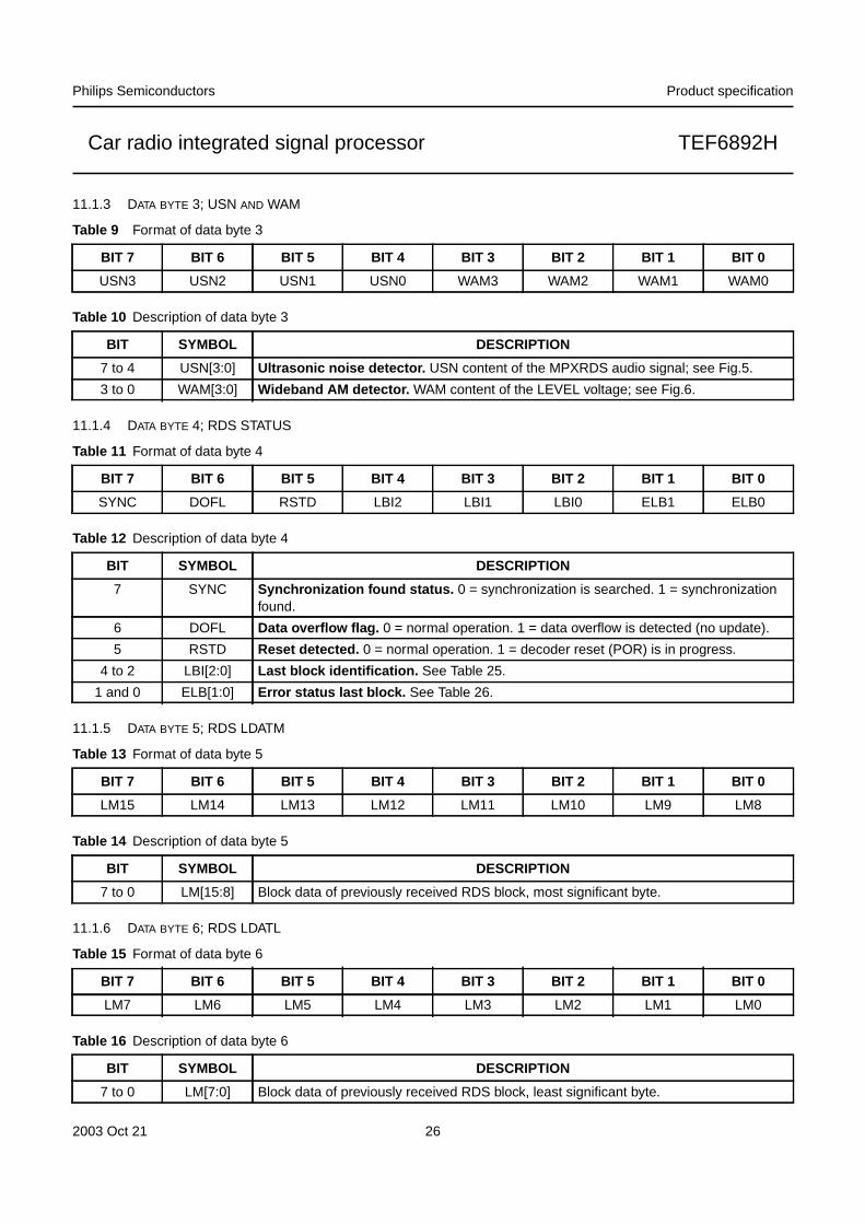
11.1.3 DATA BYTE 3; USN AND WAM
Table 9 Format of data byte 3
Table 10 Description of data byte 3
11.1.4 DATA BYTE 4; RDS STATUS
Table 11 Format of data byte 4
Table 12 Description of data byte 4
11.1.5 DATA BYTE 5; RDS LDATM
Table 13 Format of data byte 5
Table 14 Description of data byte 5
11.1.6 DATA BYTE 6; RDS LDATL
Table 15 Format of data byte 6
Table 16 Description of data byte 6
BIT 7 BIT 6 BIT 5 BIT 4 BIT 3 BIT 2 BIT 1 BIT 0
USN3 USN2 USN1 USN0 WAM3 WAM2 WAM1 WAM0
BIT SYMBOL DESCRIPTION
7 to 4 USN[3:0] Ultrasonic noise detector. USN content of the MPXRDS audio signal; see Fig.5.
3 to 0 WAM[3:0] Wideband AM detector. WAM content of the LEVEL voltage; see Fig.6.
BIT 7 BIT 6 BIT 5 BIT 4 BIT 3 BIT 2 BIT 1 BIT 0
SYNC DOFL RSTD LBI2 LBI1 LBI0 ELB1 ELB0
BIT SYMBOL DESCRIPTION
7 SYNC Synchronization found status. 0 = synchronization is searched. 1 = synchronizationfound.
6 DOFL Data overflow flag. 0 = normal operation. 1 = data overflow is detected (no update).
5 RSTD Reset detected. 0 = normal operation. 1 = decoder reset (POR) is in progress.
4 to 2 LBI[2:0] Last block identification. See Table 25.
1 and 0 ELB[1:0] Error status last block. See Table 26.
BIT 7 BIT 6 BIT 5 BIT 4 BIT 3 BIT 2 BIT 1 BIT 0
LM15 LM14 LM13 LM12 LM11 LM10 LM9 LM8
BIT SYMBOL DESCRIPTION
7 to 0 LM[15:8] Block data of previously received RDS block, most significant byte.
BIT 7 BIT 6 BIT 5 BIT 4 BIT 3 BIT 2 BIT 1 BIT 0
LM7 LM6 LM5 LM4 LM3 LM2 LM1 LM0
BIT SYMBOL DESCRIPTION
7 to 0 LM[7:0] Block data of previously received RDS block, least significant byte.
2003 Oct 21 27
Philips Semiconductors Product specification
Car radio integrated signal processor TEF6892H
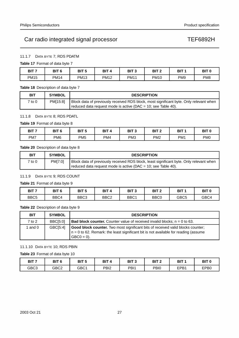
11.1.7 DATA BYTE 7; RDS PDATM
Table 17 Format of data byte 7
Table 18 Description of data byte 7
11.1.8 DATA BYTE 8; RDS PDATL
Table 19 Format of data byte 8
Table 20 Description of data byte 8
11.1.9 DATA BYTE 9; RDS COUNT
Table 21 Format of data byte 9
Table 22 Description of data byte 9
11.1.10 DATA BYTE 10; RDS PBIN
Table 23 Format of data byte 10
BIT 7 BIT 6 BIT 5 BIT 4 BIT 3 BIT 2 BIT 1 BIT 0
PM15 PM14 PM13 PM12 PM11 PM10 PM9 PM8
BIT SYMBOL DESCRIPTION
7 to 0 PM[15:8] Block data of previously received RDS block, most significant byte. Only relevant whenreduced data request mode is active (DAC = 10; see Table 40).
BIT 7 BIT 6 BIT 5 BIT 4 BIT 3 BIT 2 BIT 1 BIT 0
PM7 PM6 PM5 PM4 PM3 PM2 PM1 PM0
BIT SYMBOL DESCRIPTION
7 to 0 PM[7:0] Block data of previously received RDS block, least significant byte. Only relevant whenreduced data request mode is active (DAC = 10; see Table 40).
BIT 7 BIT 6 BIT 5 BIT 4 BIT 3 BIT 2 BIT 1 BIT 0
BBC5 BBC4 BBC3 BBC2 BBC1 BBC0 GBC5 GBC4
BIT SYMBOL DESCRIPTION
7 to 2 BBC[5:0] Bad block counter. Counter value of received invalid blocks; n = 0 to 63.
1 and 0 GBC[5:4] Good block counter. Two most significant bits of received valid blocks counter;n = 0 to 62. Remark: the least significant bit is not available for reading (assumeGBC0 = 0).
BIT 7 BIT 6 BIT 5 BIT 4 BIT 3 BIT 2 BIT 1 BIT 0
GBC3 GBC2 GBC1 PBI2 PBI1 PBI0 EPB1 EPB0
2003 Oct 21 28
Philips Semiconductors Product specification
Car radio integrated signal processor TEF6892H
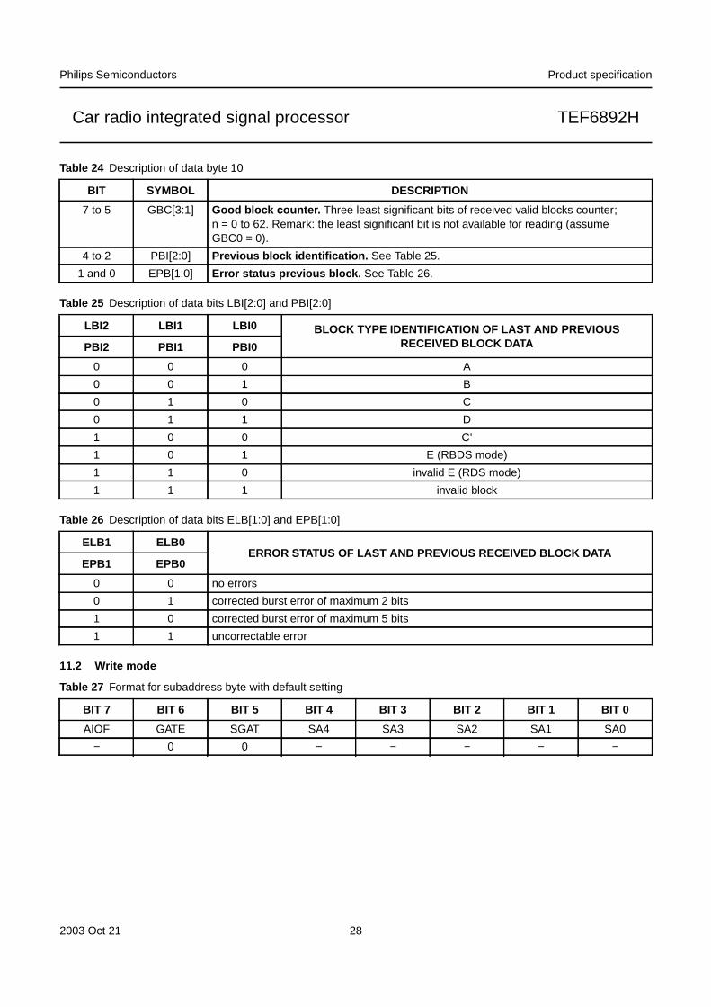
Table 24 Description of data byte 10
Table 25 Description of data bits LBI[2:0] and PBI[2:0]
Table 26 Description of data bits ELB[1:0] and EPB[1:0]
11.2 Write mode
Table 27 Format for subaddress byte with default setting
BIT SYMBOL DESCRIPTION
7 to 5 GBC[3:1] Good block counter. Three least significant bits of received valid blocks counter;n = 0 to 62. Remark: the least significant bit is not available for reading (assumeGBC0 = 0).
4 to 2 PBI[2:0] Previous block identification. See Table 25.
1 and 0 EPB[1:0] Error status previous block. See Table 26.
LBI2 LBI1 LBI0 BLOCK TYPE IDENTIFICATION OF LAST AND PREVIOUSRECEIVED BLOCK DATAPBI2 PBI1 PBI0
0 0 0 A
0 0 1 B
0 1 0 C
0 1 1 D
1 0 0 C’
1 0 1 E (RBDS mode)
1 1 0 invalid E (RDS mode)
1 1 1 invalid block
ELB1 ELB0ERROR STATUS OF LAST AND PREVIOUS RECEIVED BLOCK DATA
EPB1 EPB0
0 0 no errors
0 1 corrected burst error of maximum 2 bits
1 0 corrected burst error of maximum 5 bits
1 1 uncorrectable error
BIT 7 BIT 6 BIT 5 BIT 4 BIT 3 BIT 2 BIT 1 BIT 0
AIOF GATE SGAT SA4 SA3 SA2 SA1 SA0
− 0 0 − − − − −
2003 Oct 21 29
Philips Semiconductors Product specification
Car radio integrated signal processor TEF6892H
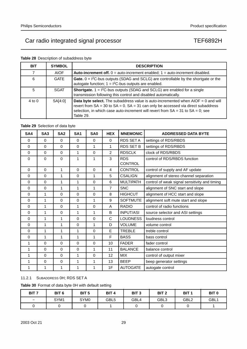
Table 28 Description of subaddress byte
Table 29 Selection of data byte
11.2.1 SUBADDRESS 0H; RDS SET A
Table 30 Format of data byte 0H with default setting
BIT SYMBOL DESCRIPTION
7 AIOF Auto-increment off. 0 = auto-increment enabled; 1 = auto-increment disabled.
6 GATE Gate. 0 = I2C-bus outputs (SDAG and SCLG) are controllable by the shortgate or theautogate function; 1 = I2C-bus outputs are enabled.
5 SGAT Shortgate. 1 = I2C-bus outputs (SDAG and SCLG) are enabled for a singletransmission following this control and disabled automatically.
4 to 0 SA[4:0] Data byte select. The subaddress value is auto-incremented when AIOF = 0 and willrevert from SA = 30 to SA = 0. SA = 31 can only be accessed via direct subaddressselection, in which case auto-increment will revert from SA = 31 to SA = 0; seeTable 29.
SA4 SA3 SA2 SA1 SA0 HEX MNEMONIC ADDRESSED DATA BYTE
0 0 0 0 0 0 RDS SET A settings of RDS/RBDS
0 0 0 0 1 1 RDS SET B settings of RDS/RBDS
0 0 0 1 0 2 RDSCLK clock of RDS/RBDS
0 0 0 1 1 3 RDSCONTROL
control of RDS/RBDS function
0 0 1 0 0 4 CONTROL control of supply and AF update
0 0 1 0 1 5 CSALIGN alignment of stereo channel separation
0 0 1 1 0 6 MULTIPATH control of weak signal sensitivity and timing
0 0 1 1 1 7 SNC alignment of SNC start and slope
0 1 0 0 0 8 HIGHCUT alignment of HCC start and slope
0 1 0 0 1 9 SOFTMUTE alignment soft mute start and slope
0 1 0 1 0 A RADIO control of radio functions
0 1 0 1 1 B INPUT/ASI source selector and ASI settings
0 1 1 0 0 C LOUDNESS loudness control
0 1 1 0 1 D VOLUME volume control
0 1 1 1 0 E TREBLE treble control
0 1 1 1 1 F BASS bass control
1 0 0 0 0 10 FADER fader control
1 0 0 0 1 11 BALANCE balance control
1 0 0 1 0 12 MIX control of output mixer
1 0 0 1 1 13 BEEP beep generator settings
1 1 1 1 1 1F AUTOGATE autogate control
BIT 7 BIT 6 BIT 5 BIT 4 BIT 3 BIT 2 BIT 1 BIT 0
− SYM1 SYM0 GBL5 GBL4 GBL3 GBL2 GBL1
0 0 0 1 0 0 0 1

2003 Oct 21 30
Philips Semiconductors Product specification
Car radio integrated signal processor TEF6892H
Table 31 Description of data byte 0H
Table 32 Description of synchronization mode
11.2.2 SUBADDRESS 1H; RDS SET B
Table 33 Format of data byte 1H with default setting
Table 34 Description of data byte 1H
11.2.3 SUBADDRESS 2H; RDSCLK
Table 35 Format of data byte 2H with default setting
BIT SYMBOL DESCRIPTION
7 − Not used. Set to logic 0.
6 and 5 SYM[1:0] Synchronization mode. See Table 32.
4 to 0 GBL[5:1] Maximum good blocks lose (0 to 63). Number of valid blocks (good blocks counter) atwhich both the good block counter and the bad block counter are reset to 0. Only usedwhen synchronized. GBL0 is located in byte RDS SET B.When the bad block counter reaches value BBL (see byte RDS SET B) before thegood block counter reaches value GBL a new synchronization is started.
SYM1 SYM0 SYNCHRONIZATION MODE
0 0 no error correction; only error free blocks are handled as valid
0 1 limited error correction; up to 2 bits error correctable blocks are handled as valid
1 0 full error correction; up to 5 bits error correctable blocks are handled as valid
1 1 mixed mode; only error free blocks are handled as valid for synchronization search, butwhen synchronized, up to 5 bits error correctable blocks are handled as valid
BIT 7 BIT 6 BIT 5 BIT 4 BIT 3 BIT 2 BIT 1 BIT 0
GBL0 RBDS BBL5 BBL4 BBL3 BBL2 BBL1 BBL0
0 0 0 0 0 0 0 1
BIT SYMBOL DESCRIPTION
7 GBL0 Maximum good blocks lose (0 to 63); see Table 31.
6 RBDS RBDS mode. 0 = RDS mode, RBDS type E blocks are handled as invalid (bad block);1 = RBDS mode, RBDS type E blocks are handled as valid (good block).
5 to 0 BBL[5:0] Maximum bad blocks lose (0 to 63). Number of invalid blocks (bad blocks counter) atwhich a new synchronization is started. Both the good block counter and the bad blockcounter are reset to 0.
BIT 7 BIT 6 BIT 5 BIT 4 BIT 3 BIT 2 BIT 1 BIT 0
− − TST3 TST2 TST1 TST0 CLKO CLKI
− − 0 0 0 0 0 1

2003 Oct 21 31
Philips Semiconductors Product specification
Car radio integrated signal processor TEF6892H
Table 36 Description of data byte 2H
Table 37 RDS clock description
11.2.4 SUBADDRESS 3H; RDS CONTROL
Table 38 Format of data byte 3H with default setting
Table 39 Description of data byte 3H
Table 40 Description of data available control
BIT SYMBOL DESCRIPTION
7 and 6 − Not used. Set to logic 0.
5 to 2 TST[3:0] Test. TST[3:0] = 0000: normal operation.
1 CLKO Clock input or output and buffered or unbuffered raw RDS output. See Table 37.
0 CLKI
CLKO CLKI RDS/RBDS CLOCK
0 0 RDS decoder mode; pin RDCL is disabled
0 1 for RDS decoder bypass mode; RDCL is burst clock input for raw RDS read-out
1 0 for RDS decoder mode: continuous block rate data available signal at pin RDCL;for RDS decoder bypass mode: RDCL is clock output for raw RDS read-out
1 1 reserved
BIT 7 BIT 6 BIT 5 BIT 4 BIT 3 BIT 2 BIT 1 BIT 0
DAC1 DAC0 NWSY BBG4 BBG3 BBG2 BBG1 BBG0
0 0 0 0 0 0 0 0
BIT SYMBOL DESCRIPTION
7 and 6 DAC[1:0] Data available control. See Table 40.
5 NWSY New synchronization search. 0 = synchronization is started by BBL value of bad blockcounter only; 1 = restart of synchronization search. NWSY is automatically reset tologic 0.
4 to 0 BBG[4:0] Maximum bad blocks gain. Number of invalid blocks (bad block counter) that isallowed during synchronization search. If reached, a new synchronization is started.BBG[4:0] = 0 disables this function.
DAC1 DAC0 DATA AVAILABLE CONTROL
0 0 standard output mode; new block data is signalled at every new received block
0 1 fast PI search mode; during synchronization search (SYNC = 0) A or C’ block data isavailable and signalled, when synchronized standard output mode is active
1 0 reduced data request mode; when synchronized new block data is signalled every twonew received blocks
1 1 decoder bypass mode; raw RDS data from demodulator is available on pin RDDA
2003 Oct 21 32
Philips Semiconductors Product specification
Car radio integrated signal processor TEF6892H
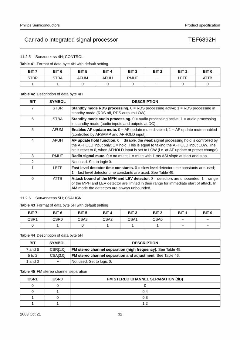
11.2.5 SUBADDRESS 4H; CONTROL
Table 41 Format of data byte 4H with default setting
Table 42 Description of data byte 4H
11.2.6 SUBADDRESS 5H; CSALIGN
Table 43 Format of data byte 5H with default setting
Table 44 Description of data byte 5H
Table 45 FM stereo channel separation
BIT 7 BIT 6 BIT 5 BIT 4 BIT 3 BIT 2 BIT 1 BIT 0
STBR STBA AFUM AFUH RMUT − LETF ATTB
1 1 0 0 0 − 0 0
BIT SYMBOL DESCRIPTION
7 STBR Standby mode RDS processing. 0 = RDS processing active; 1 = RDS processing instandby mode (RDS off, RDS outputs LOW).
6 STBA Standby mode audio processing. 0 = audio processing active; 1 = audio processingin standby mode (audio inputs and outputs at DC).
5 AFUM Enables AF update mute. 0 = AF update mute disabled; 1 = AF update mute enabled(controlled by AFSAMP and AFHOLD input).
4 AFUH AF update hold function. 0 = disable, the weak signal processing hold is controlled bythe AFHOLD input only; 1 = hold. This is equal to taking the AFHOLD input LOW. Thebit is reset to 0, when AFHOLD input is set to LOW (i.e. at AF update or preset change).
3 RMUT Radio signal mute. 0 = no mute; 1 = mute with 1 ms ASI slope at start and stop.
2 − Not used. Set to logic 0.
1 LETF Fast level detector time constants. 0 = slow level detector time constants are used;1 = fast level detector time constants are used. See Table 49.
0 ATTB Attack bound of the MPH and LEV detector. 0 = detectors are unbounded; 1 = rangeof the MPH and LEV detector are limited in their range for immediate start of attack. InAM mode the detectors are always unbounded.
BIT 7 BIT 6 BIT 5 BIT 4 BIT 3 BIT 2 BIT 1 BIT 0
CSR1 CSR0 CSA3 CSA2 CSA1 CSA0 − −0 1 0 1 1 1 − −
BIT SYMBOL DESCRIPTION
7 and 6 CSR[1:0] FM stereo channel separation (high frequency). See Table 45.
5 to 2 CSA[3:0] FM stereo channel separation and adjustment. See Table 46.
1 and 0 − Not used. Set to logic 0.
CSR1 CSR0 FM STEREO CHANNEL SEPARATION (dB)
0 0 0
0 1 0.4
1 0 0.8
1 1 1.2

2003 Oct 21 33
Philips Semiconductors Product specification
Car radio integrated signal processor TEF6892H
Table 46 FM stereo channel separation and adjustment
11.2.7 SUBADDRESS 6H; MULTIPATH
Table 47 Format of data byte 6H with default setting
Table 48 Description of data byte 6H
Table 49 Setting of the time constants of the LEVEL detector
Table 50 Setting of the time constants of the MPH detector (level, WAM and USN)
CSA3 CSA2 CSA1 CSA0FM STEREO CHANNEL SEPARATION AND
ADJUSTMENT (dB)
0 0 0 0 0
0 0 0 1 0.2
: : : : :
1 1 1 0 2.8
1 1 1 1 3.0
BIT 7 BIT 6 BIT 5 BIT 4 BIT 3 BIT 2 BIT 1 BIT 0
USS1 USS0 WAS1 WAS0 LET1 LET0 MPT1 MPT0
0 1 0 1 0 0 0 0
BIT SYMBOL DESCRIPTION
7 and 6 USS[1:0] USN sensitivity for weak signal processing. See Fig.5.
5 and 4 WAS[1:0] WAM sensitivity for weak signal processing. See Fig.6.
3 and 2 LET[1:0] LEVEL detector time constant. See Table 49.
1 and 0 MPT[1:0] MPH detector time constants (level, WAM and USN). See Table 50.
LETF LET1 LET0tLEVEL (s)
ATTACK DECAY
0 0 0 3 3
0 0 1 3 6
0 1 0 1.5 1.5
0 1 1 0.5 1.5
1 0 0 0.5 0.5
1 0 1 0.17 0.5
1 1 0 0.06 0.17
1 1 1 0.06 0.06
MPT1 MPT0tMPH (s)
ATTACK DECAY
0 0 0.5 12
0 1 0.5 24
1 0 0.5 6
1 1 0.25 6
2003 Oct 21 34
Philips Semiconductors Product specification
Car radio integrated signal processor TEF6892H
handbook, halfpage
0 1.25
VMPXRDS(rms) (V)
Veq(V)
5
0
1
2
3
4
0.25 0.5 0.75 1
MHC332
(1) (2) (3) (4)
Fig.5 Equivalent level voltage Veq (USN and MPHdetector) as a function of MPX signal at150 kHz.
(1) USS[1:0] = 11 = −6 V/0.5 V.
(2) USS[1:0] = 10 = −4 V/0.5 V.
(3) USS[1:0] = 01 = −3 V/0.5 V.
(4) USS[1:0] = 00 = −2 V/0.5 V.
handbook, halfpage
0 1VLEVEL(p-p) (V)
Veq(V)
5
0
1
2
3
4
0.2 0.4 0.6 0.8
MHC333
(1) (2) (3) (4)
Fig.6 Equivalent level voltage Veq (WAM andMPH detector) as a function of level input at21 kHz.
(1) WAS[1:0] = 11 = −6 V/0.4 V.
(2) WAS[1:0] = 10 = −4 V/0.4 V.
(3) WAS[1:0] = 01 = −3 V/0.4 V.
(4) WAS[1:0] = 00 = −2 V/0.4 V.
11.2.8 SUBADDRESS 7H; SNC
Table 51 Format of data byte 7H with default setting
Table 52 Description of data byte 7H
BIT 7 BIT 6 BIT 5 BIT 4 BIT 3 BIT 2 BIT 1 BIT 0
SST3 SST2 SST1 SST0 SSL1 SSL0 HCMP HCSF
0 1 1 1 0 1 0 0
BIT SYMBOL DESCRIPTION
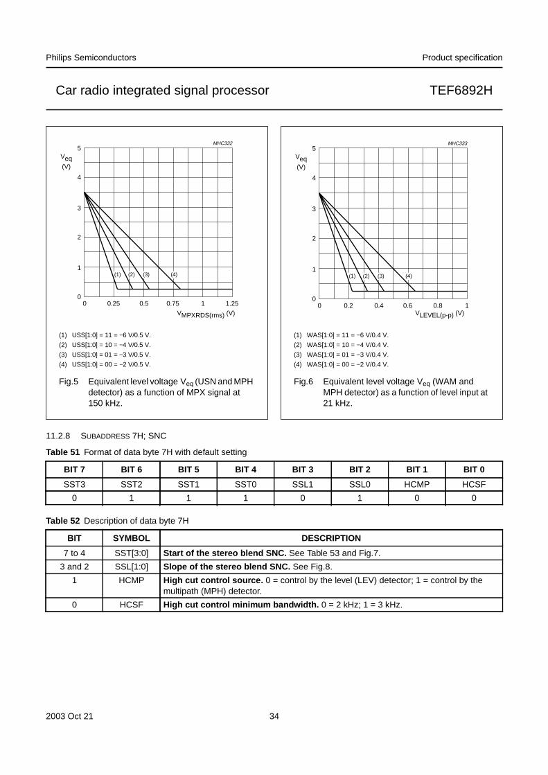
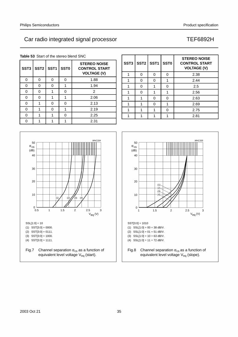
7 to 4 SST[3:0] Start of the stereo blend SNC. See Table 53 and Fig.7.
3 and 2 SSL[1:0] Slope of the stereo blend SNC. See Fig.8.
1 HCMP High cut control source. 0 = control by the level (LEV) detector; 1 = control by themultipath (MPH) detector.
0 HCSF High cut control minimum bandwidth. 0 = 2 kHz; 1 = 3 kHz.
2003 Oct 21 35
Philips Semiconductors Product specification
Car radio integrated signal processor TEF6892H
Table 53 Start of the stereo blend SNC
SST3 SST2 SST1 SST0STEREO NOISE
CONTROL STARTVOLTAGE (V)
0 0 0 0 1.88
0 0 0 1 1.94
0 0 1 0 2
0 0 1 1 2.06
0 1 0 0 2.13
0 1 0 1 2.19
0 1 1 0 2.25
0 1 1 1 2.31
1 0 0 0 2.38
1 0 0 1 2.44
1 0 1 0 2.5
1 0 1 1 2.56
1 1 0 0 2.63
1 1 0 1 2.69
1 1 1 0 2.75
1 1 1 1 2.81
SST3 SST2 SST1 SST0STEREO NOISE
CONTROL STARTVOLTAGE (V)
handbook, halfpage
0.5 3Veq (V)
αcs(dB)
50
0
10
20
30
40
1 1.5 2 2.5
MHC334
(1) (2) (3) (4)
Fig.7 Channel separation αcs as a function ofequivalent level voltage Veq (start).
SSL[1:0] = 10
(1) SST[3:0] = 0000.
(2) SST[3:0] = 0111.
(3) SST[3:0] = 1000.
(4) SST[3:0] = 1111.
handbook, halfpage
3Veq (V)
αcs(dB)
50
0
10
20
30
40
1 1.5 2 2.5
MHC335
(4)(3)(2)(1)
Fig.8 Channel separation αcs as a function ofequivalent level voltage Veq (slope).
SST[3:0] = 1010
(1) SSL[1:0] = 00 = 38 dB/V.
(2) SSL[1:0] = 01 = 51 dB/V.
(3) SSL[1:0] = 10 = 63 dB/V.
(4) SSL[1:0] = 11 = 72 dB/V.

2003 Oct 21 36
Philips Semiconductors Product specification
Car radio integrated signal processor TEF6892H
11.2.9 SUBADDRESS 8H; HIGHCUT
Table 54 Format of data byte 8H with default setting
Table 55 Description of data byte 8H
BIT 7 BIT 6 BIT 5 BIT 4 BIT 3 BIT 2 BIT 1 BIT 0
HST2 HST1 HST0 HSL1 HSL0 HCF2 HCF1 HCF0
0 1 1 0 1 1 1 1
BIT SYMBOL DESCRIPTION
7 to 5 HST[2:0] High cut control start (weak signal processing). See Fig.9.
4 and 3 HSL[1:0] High cut control slope (weak signal processing). See Fig.10.
2 to 0 HCF[2:0] Fixed high cut control (maximum HCC bandwidth). See Table 56 and Fig.11.
handbook, full pagewidth
MHC336
0 0.5Veq (V)
1 21.5
αHCC(dB)
2.5 3 3.5
0
12
15
9
6
3
(1) (2) (3) (4) (5) (6) (7) (8)
Fig.9 High cut control attenuation αHCC as a function of equivalent level voltage Veq (start).
(5) HST[2:0] = 100 = 2.5 V.
(6) HST[2:0] = 101 = 3 V.
(7) HST[2:0] = 110 = 3.5 V.
(8) HST[2:0] = 111 = 4 V.
HCF[2:0] = 111, HCSF = 0,HSL[1:0] = 10 and faudio = 10 kHz
(1) HST[2:0] = 000 = 1.5 V.
(2) HST[2:0] = 001 = 1.75 V.
(3) HST[2:0] = 010 = 2 V.
(4) HST[2:0] = 011 = 2.25 V.

2003 Oct 21 37
Philips Semiconductors Product specification
Car radio integrated signal processor TEF6892H
Table 56 Fixed high cut control
handbook, halfpage
0 0.5Veq (V)
1 21.5
αHCC(dB)
2.5
0
Bmax(kHz)
unlimited
wide
10
6.8
4.7
3.3
2.2
1.5
18
12
15
9
6
3
MHC337
HCSF = 0
HCSF = 1
(1) (2)(3) (4)
Fig.10 High cut control attenuation αHCC as afunction of equivalent level voltage Veq(slope).
HST[2:0] = 010 and faudio = 10 kHz
(1) HSL[1:0] = 00 = 9 dB/V.
(2) HSL[1:0] = 01 = 11 dB/V.
(3) HSL[1:0] = 10 = 14 dB/V.
(4) HSL[1:0] = 11 = 18 dB/V.
HCF2 HCF1 HCF0 Bmax (kHz)
0 0 0 1.5
0 0 1 2.2
0 1 0 3.3
0 1 1 4.7
1 0 0 6.8
1 0 1 10
1 1 0 wide
1 1 1 unlimited
handbook, full pagewidth
−24
−20
−16
−12
−8
−4
−22
−18
−14
−10
−6
−2
6
4
2
0
MHC338
10
GHCC(dB)
faudio (Hz)102 103 104 105
Fig.11 High cut control gain GHCC as a function of audio frequency faudio (fixed HCC).
2003 Oct 21 38
Philips Semiconductors Product specification
Car radio integrated signal processor TEF6892H
11.2.10 SUBADDRESS 9H; SOFTMUTE
Table 57 Format of data byte 9H with default setting
Table 58 Description of data byte 9H
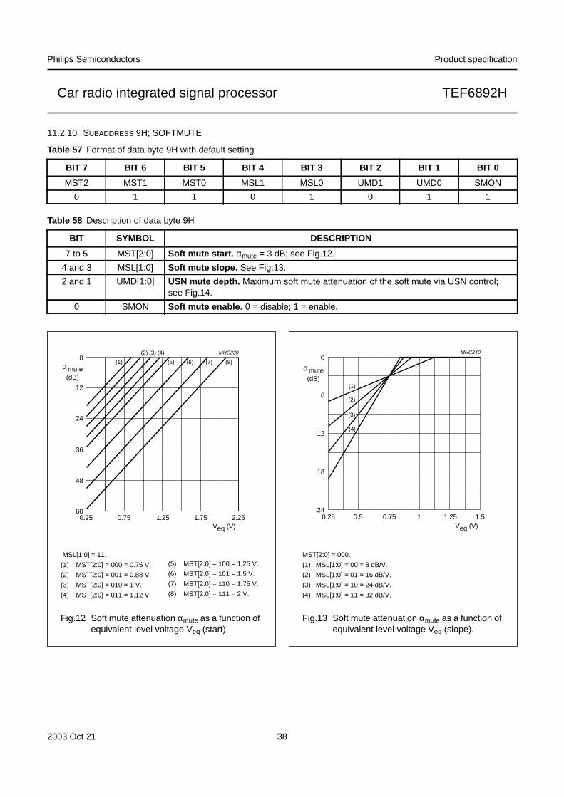
BIT 7 BIT 6 BIT 5 BIT 4 BIT 3 BIT 2 BIT 1 BIT 0
MST2 MST1 MST0 MSL1 MSL0 UMD1 UMD0 SMON
0 1 1 0 1 0 1 1
BIT SYMBOL DESCRIPTION
7 to 5 MST[2:0] Soft mute start. αmute = 3 dB; see Fig.12.
4 and 3 MSL[1:0] Soft mute slope. See Fig.13.
2 and 1 UMD[1:0] USN mute depth. Maximum soft mute attenuation of the soft mute via USN control;see Fig.14.
0 SMON Soft mute enable. 0 = disable; 1 = enable.
handbook, halfpage
0.25 0.75Veq (V)
1.25 1.75
αmute(dB)
2.25
0
60
48
36
24
12
MHC339
(1) (5) (6) (7) (8)
(2) (3) (4)
Fig.12 Soft mute attenuation αmute as a function ofequivalent level voltage Veq (start).
(5) MST[2:0] = 100 = 1.25 V.
(6) MST[2:0] = 101 = 1.5 V.
(7) MST[2:0] = 110 = 1.75 V.
(8) MST[2:0] = 111 = 2 V.
MSL[1:0] = 11.
(1) MST[2:0] = 000 = 0.75 V.
(2) MST[2:0] = 001 = 0.88 V.
(3) MST[2:0] = 010 = 1 V.
(4) MST[2:0] = 011 = 1.12 V.
handbook, halfpage
0.25 0.5 1.5Veq (V)
0
6
18
24
12
0.75 1
αmute(dB)
1.25
MHC340
(4)
(2)
(1)
(3)
Fig.13 Soft mute attenuation αmute as a function ofequivalent level voltage Veq (slope).
MST[2:0] = 000.
(1) MSL[1:0] = 00 = 8 dB/V.
(2) MSL[1:0] = 01 = 16 dB/V.
(3) MSL[1:0] = 10 = 24 dB/V.
(4) MSL[1:0] = 11 = 32 dB/V.

2003 Oct 21 39
Philips Semiconductors Product specification
Car radio integrated signal processor TEF6892H
handbook, halfpage
0.25 0.5 1.5Veq (V)
0
6
18
24
12
0.75 1
αmute(dB)
1.25
MHC341
(1) a b
(2)
(3)
(4)
Fig.14 Soft mute depth αmute caused by ultrasonic noise.
a. MST[2:0] = 000, MSL[1:0] = 11
b. MST[2:0] = 100, MSL[1:0] = 01
(1) UMD[1:0] = 00 = 3 dB.
(2) UMD[1:0] = 01 = 6 dB.
(3) UMD[1:0] = 10 = 9 dB.
(4) UMD[1:0] = 11 = 12 dB.
11.2.11 SUBADDRESS AH; RADIO
Table 59 Format of data byte AH with default setting
Table 60 Description of data byte AH
BIT 7 BIT 6 BIT 5 BIT 4 BIT 3 BIT 2 BIT 1 BIT 0
AM MONO DEMP ING1 ING0 SEAR NBS1 NBS0
0 0 1 0 0 1 1 0
BIT SYMBOL DESCRIPTION
7 AM AM selection. 0 = FM mode selected; 1 = AM mode selected.
6 MONO Stereo decoder mono. 0 = set to FM stereo; 1 = set to FM mono.
5 DEMP De-emphasis time constant. 0 = 75 µs; 1 = 50 µs; see Fig.15.
4 and 3 ING[1:0] Input gain. See Table 61.
2 SEAR LEVEL and MPH detector time constant. 0 = standard time constant selected;1 = fast time constant of 60 ms selected.
1 and 0 NBS[1:0] AM noise blanker and the FM noise blanker MPX sensitivity. See Table 62.
2003 Oct 21 40
Philips Semiconductors Product specification
Car radio integrated signal processor TEF6892H
Table 61 Input gain Table 62 Noise blanker sensitivity
ING1 ING0GAIN FOR
FMMPX INPUT(dB)
GAIN FOR AMAND MPXRDS
INPUT (dB)
0 0 0 0
0 1 3 3
1 0 6 6
1 1 23.5 0
NBS1 NBS0
SENSITIVITYOF FM NOISEBLANKER AT
MPXRDS INPUT(mV)
SENSITIVITYOF AM NOISEBLANKER (%)
0 0 90 110
0 1 150 140
1 0 210 175
1 1 270 220
Fig.15 De-emphasis gain Gde-em as a function of audio frequency faudio.
(1) τde-em = 50 µs.
(2) τde-em = 75 µs.
handbook, full pagewidth
−24
−20
−16
−12
−8
−4
−22
−18
−14
−10
−6
−2
6
4
2
0
MHC342
10
(1)
(2)
Gde-em(dB)
faudio (Hz)102 103 104 105
2003 Oct 21 41
Philips Semiconductors Product specification
Car radio integrated signal processor TEF6892H
11.2.12 SUBADDRESS BH; INPUT AND ASI
Table 63 Format of data byte BH with default setting
Table 64 Description of data byte BH
Table 65 FM noise blanker level sensitivity
Table 66 Audio input tone/volume part
Table 67 Audio step interpolation time constant
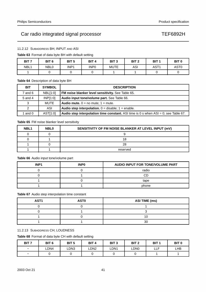
11.2.13 SUBADDRESS CH; LOUDNESS
Table 68 Format of data byte CH with default setting
BIT 7 BIT 6 BIT 5 BIT 4 BIT 3 BIT 2 BIT 1 BIT 0
NBL1 NBL0 INP1 INP0 MUTE ASI AST1 AST0
1 0 0 0 1 1 0 0
BIT SYMBOL DESCRIPTION
7 and 6 NBL[1:0] FM noise blanker level sensitivity. See Table 65.
5 and 4 INP[1:0] Audio input tone/volume part. See Table 66.
3 MUTE Audio mute. 0 = no mute; 1 = mute.
2 ASI Audio step interpolation. 0 = disable; 1 = enable.
1 and 0 AST[1:0] Audio step interpolation time constant. ASI time is 0 s when ASI = 0; see Table 67.
NBL1 NBL0 SENSITIVITY OF FM NOISE BLANKER AT LEVEL INPUT (mV)
0 0 9
0 1 18
1 0 28
1 1 reserved
INP1 INP0 AUDIO INPUT FOR TONE/VOLUME PART
0 0 radio
0 1 CD
1 0 tape
1 1 phone
AST1 AST0 ASI TIME (ms)
0 0 1
0 1 3
1 0 10
1 1 30
BIT 7 BIT 6 BIT 5 BIT 4 BIT 3 BIT 2 BIT 1 BIT 0
− LDN4 LDN3 LDN2 LDN1 LDN0 LLF LHB
− 0 0 0 0 0 1 1

2003 Oct 21 42
Philips Semiconductors Product specification
Car radio integrated signal processor TEF6892H
Table 69 Description of data byte CH, see Figs 16 to 19
Table 70 Loudness gain
BIT SYMBOL DESCRIPTION
7 − Not used. Set to logic 0.
6 to 2 LDN[4:0] Loudness gain. See Table 70.
1 LLF Loudness low boost frequency. 0 = 50 Hz; 1 = 100 Hz.
0 LHB Loudness high boost enable. 0 = loudness low boost is enabled; 1 = loudness lowboost and loudness high boost are enabled.
LDN4 LDN3 LDN2 LDN1 LDN0 LOUDNESS CONTROL (dB)
0 0 0 0 0 0
0 0 0 0 1 −1
0 0 0 1 0 −2
: : : : : :
1 0 0 1 0 −18
1 0 0 1 1 −19
1 0 1 0 0 −20
handbook, full pagewidth
−24
−20
−16
−12
−8
−4
−22
−18
−14
−10
−6
−2
6
4
2
0
MHC343
10
Gloudness(dB)
faudio (Hz)102 103 104 105
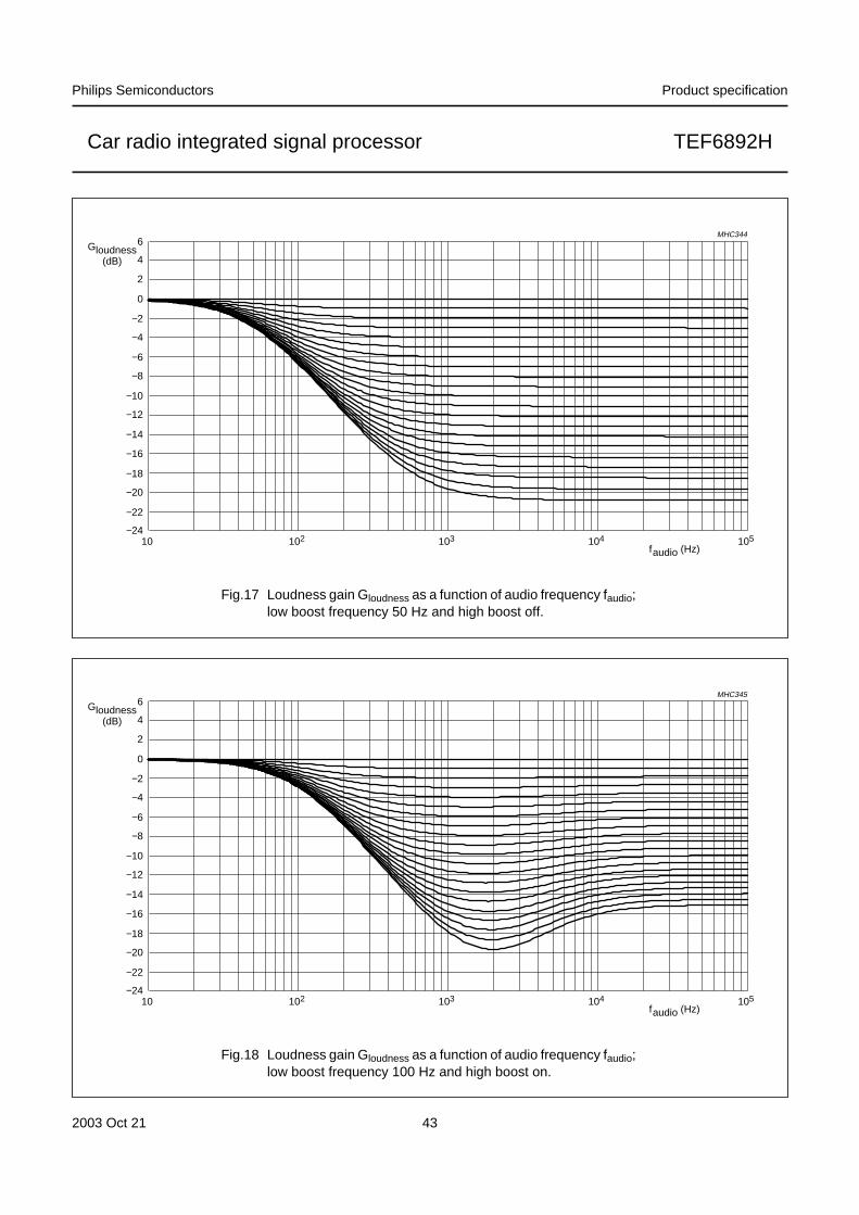
Fig.16 Loudness gain Gloudness as a function of audio frequency faudio;low boost frequency 50 Hz and high boost on.
2003 Oct 21 43
Philips Semiconductors Product specification
Car radio integrated signal processor TEF6892H
handbook, full pagewidth
−24
−20
−16
−12
−8
−4
−22
−18
−14
−10
−6
−2
6
4
2
0
MHC344
10
Gloudness(dB)
faudio (Hz)102 103 104 105
Fig.17 Loudness gain Gloudness as a function of audio frequency faudio;low boost frequency 50 Hz and high boost off.
handbook, full pagewidth
−24
−20
−16
−12
−8
−4
−22
−18
−14
−10
−6
−2
6
4
2
0
MHC345
10
Gloudness(dB)
faudio (Hz)102 103 104 105
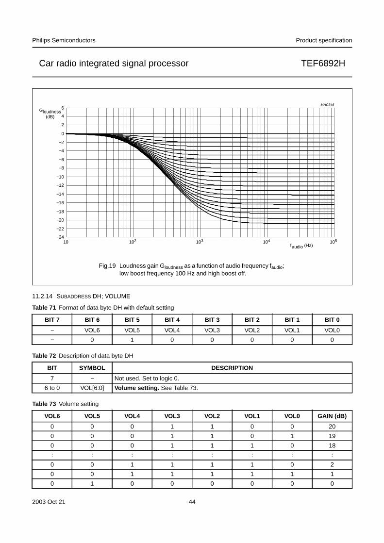
Fig.18 Loudness gain Gloudness as a function of audio frequency faudio;low boost frequency 100 Hz and high boost on.
2003 Oct 21 44
Philips Semiconductors Product specification
Car radio integrated signal processor TEF6892H
handbook, full pagewidth
−24
−20
−16
−12
−8
−4
−22
−18
−14
−10
−6
−2
6
4
2
0
MHC346
10
Gloudness(dB)
faudio (Hz)102 103 104 105
Fig.19 Loudness gain Gloudness as a function of audio frequency faudio;low boost frequency 100 Hz and high boost off.
11.2.14 SUBADDRESS DH; VOLUME
Table 71 Format of data byte DH with default setting
Table 72 Description of data byte DH
Table 73 Volume setting
BIT 7 BIT 6 BIT 5 BIT 4 BIT 3 BIT 2 BIT 1 BIT 0
− VOL6 VOL5 VOL4 VOL3 VOL2 VOL1 VOL0
− 0 1 0 0 0 0 0
BIT SYMBOL DESCRIPTION
7 − Not used. Set to logic 0.
6 to 0 VOL[6:0] Volume setting. See Table 73.
VOL6 VOL5 VOL4 VOL3 VOL2 VOL1 VOL0 GAIN (dB)
0 0 0 1 1 0 0 20
0 0 0 1 1 0 1 19
0 0 0 1 1 1 0 18
: : : : : : : :
0 0 1 1 1 1 0 2
0 0 1 1 1 1 1 1
0 1 0 0 0 0 0 0
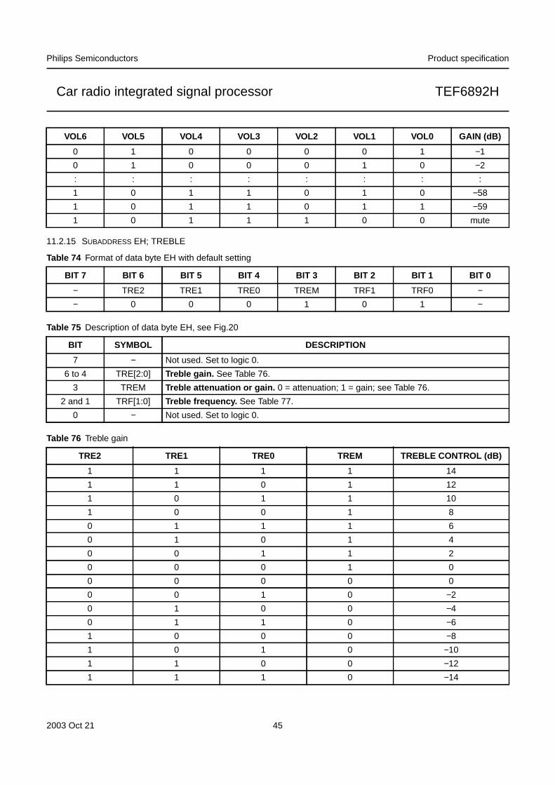
2003 Oct 21 45
Philips Semiconductors Product specification
Car radio integrated signal processor TEF6892H
11.2.15 SUBADDRESS EH; TREBLE
Table 74 Format of data byte EH with default setting
Table 75 Description of data byte EH, see Fig.20
Table 76 Treble gain
0 1 0 0 0 0 1 −1
0 1 0 0 0 1 0 −2
: : : : : : : :
1 0 1 1 0 1 0 −58
1 0 1 1 0 1 1 −59
1 0 1 1 1 0 0 mute
BIT 7 BIT 6 BIT 5 BIT 4 BIT 3 BIT 2 BIT 1 BIT 0
− TRE2 TRE1 TRE0 TREM TRF1 TRF0 −− 0 0 0 1 0 1 −
BIT SYMBOL DESCRIPTION
7 − Not used. Set to logic 0.
6 to 4 TRE[2:0] Treble gain. See Table 76.
3 TREM Treble attenuation or gain. 0 = attenuation; 1 = gain; see Table 76.
2 and 1 TRF[1:0] Treble frequency. See Table 77.
0 − Not used. Set to logic 0.
TRE2 TRE1 TRE0 TREM TREBLE CONTROL (dB)
1 1 1 1 14
1 1 0 1 12
1 0 1 1 10
1 0 0 1 8
0 1 1 1 6
0 1 0 1 4
0 0 1 1 2
0 0 0 1 0
0 0 0 0 0
0 0 1 0 −2
0 1 0 0 −4
0 1 1 0 −6
1 0 0 0 −8
1 0 1 0 −10
1 1 0 0 −12
1 1 1 0 −14
VOL6 VOL5 VOL4 VOL3 VOL2 VOL1 VOL0 GAIN (dB)

2003 Oct 21 46
Philips Semiconductors Product specification
Car radio integrated signal processor TEF6892H
Table 77 Treble frequency
TRF1 TRF0 TREBLE FREQUENCY (kHz)
0 0 8
0 1 10
1 0 12
1 1 15
Fig.20 Treble gain Gtreble as a function of audio frequency faudio, ftreble = 10 kHz.
handbook, full pagewidth
0
5
10
15
20
−20
−5
−10
−15
MHC347
10faudio (Hz)
Gtreble(dB)
102 103 104 105
11.2.16 SUBADDRESS FH; BASS
Table 78 Format of data byte FH with default setting
Table 79 Description of data byte FH, see Figs 21 and 22
BIT 7 BIT 6 BIT 5 BIT 4 BIT 3 BIT 2 BIT 1 BIT 0
− BAS2 BAS1 BAS0 BASM BAF1 BAF0 BASH
− 0 0 0 1 1 0 0
BIT SYMBOL DESCRIPTION
7 − Not used. Set to logic 0.
6 to 4 BAS[2:0] Bass gain. See Table 80.
3 BASM Bass attenuation or gain. 0 = attenuation; 1 = gain; see Table 80.
2 and 1 BAF[1:0] Bass frequency. See Table 81.
0 BASH Bass frequency response. 0 = band-pass; 1 = shelve curve (only guaranteed forBASM = 0).
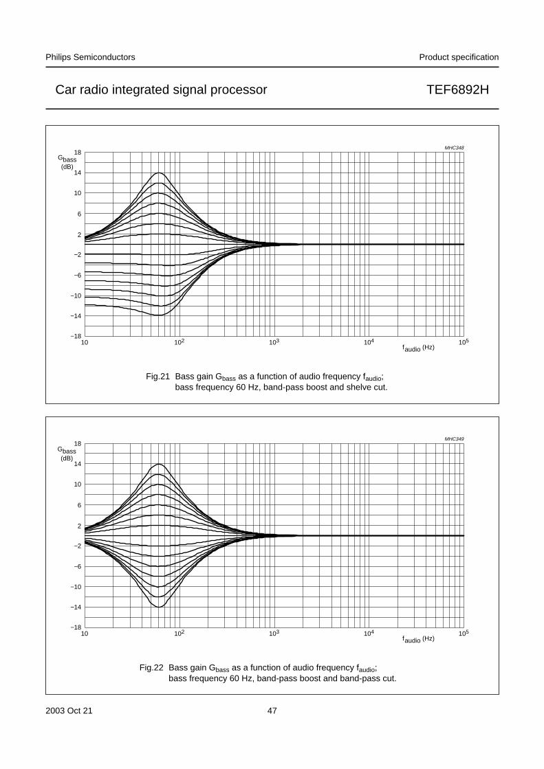
2003 Oct 21 47
Philips Semiconductors Product specification
Car radio integrated signal processor TEF6892H
handbook, full pagewidth
−18
18
14
−10
−14
10
6
2
−2
−6
MHC348
10
Gbass(dB)
faudio (Hz)102 103 104 105
Fig.21 Bass gain Gbass as a function of audio frequency faudio;bass frequency 60 Hz, band-pass boost and shelve cut.
handbook, full pagewidth
−18
18
14
−10
−14
10
6
2
−2
−6
MHC349
10
Gbass(dB)
faudio (Hz)102 103 104 105
Fig.22 Bass gain Gbass as a function of audio frequency faudio;bass frequency 60 Hz, band-pass boost and band-pass cut.
2003 Oct 21 48
Philips Semiconductors Product specification
Car radio integrated signal processor TEF6892H
Table 80 Bass gain
Table 81 Bass frequency
11.2.17 SUBADDRESS 10H; FADER
Table 82 Format of data byte 10H with default setting
Table 83 Description of data byte 10H
BAS2 BAS1 BAS0 BASM BASS CONTROL (dB)
1 1 1 1 14
1 1 0 1 12
1 0 1 1 10
1 0 0 1 8
0 1 1 1 6
0 1 0 1 4
0 0 1 1 2
0 0 0 1 0
0 0 0 0 0
0 0 1 0 −2
0 1 0 0 −4
0 1 1 0 −6
1 0 0 0 −8
1 0 1 0 −10
1 1 0 0 −12
1 1 1 0 −14
BAF1 BAF0 BASS FREQUENCY (Hz)
0 0 60
0 1 80
1 0 100
1 1 120
BIT 7 BIT 6 BIT 5 BIT 4 BIT 3 BIT 2 BIT 1 BIT 0
− − FAD4 FAD3 FAD2 FAD1 FAD0 FADM
− − 0 0 0 0 0 1
BIT SYMBOL DESCRIPTION
7 and 6 − Not used. Set to logic 0.
5 to 1 FAD[4:0] Fader gain. See Table 84.
0 FADM Fader gain mode. 0 = front output attenuated; 1 = rear output attenuated.
2003 Oct 21 49
Philips Semiconductors Product specification
Car radio integrated signal processor TEF6892H
Table 84 Fader gain
11.2.18 SUBADDRESS 11H; BALANCE
Table 85 Format of data byte 11H with default setting
Table 86 Description of data byte 11H
Table 87 Balance gain
FAD4 FAD3 FAD2 FAD1 FAD0 FADER CONTROL (dB)
0 0 0 0 0 0
0 0 0 0 1 −1
0 0 0 1 0 −2
: : : : : :
0 1 1 1 0 −14
0 1 1 1 1 −15
1 0 0 0 0 −17.5
1 0 0 0 1 −20
: : : : : :
1 1 0 1 0 −42.5
1 1 0 1 1 −45
1 1 1 0 0 −48
1 1 1 0 1 −51
1 1 1 1 0 −55
1 1 1 1 1 −59
BIT 7 BIT 6 BIT 5 BIT 4 BIT 3 BIT 2 BIT 1 BIT 0
BAL6 BAL5 BAL4 BAL3 BAL2 BAL1 BAL0 BALM
0 0 0 0 0 0 0 1
BIT SYMBOL DESCRIPTION
7 to 1 BAL[6:0] Balance gain. See Table 87.
0 BALM Balance gain mode. 0 = left channel attenuated; 1 = right channel attenuated.
BAL6 BAL5 BAL4 BAL3 BAL2 BAL1 BAL0BALANCECONTROL
(dB)
0 0 0 0 0 0 0 0
0 0 0 0 0 0 1 −1
0 0 0 0 0 1 0 −2
: : : : : : : :
1 0 0 1 1 0 1 −77
1 0 0 1 1 1 0 −78
1 0 0 1 1 1 1 −79
1 0 1 0 0 0 0 mute

2003 Oct 21 50
Philips Semiconductors Product specification
Car radio integrated signal processor TEF6892H
11.2.19 SUBADDRESS 12H; MIX
Table 88 Format of data byte 12H with default setting
Table 89 Description of data byte 12H
11.2.20 SUBADDRESS 13H; BEEP
Table 90 Format of data byte 13H with default setting
Table 91 Description of data byte 13H
Table 92 Beep level
BIT 7 BIT 6 BIT 5 BIT 4 BIT 3 BIT 2 BIT 1 BIT 0
MILF MIRF MILR MIRR MULF MURF MULR MURR
0 0 0 0 1 1 1 1
BIT SYMBOL DESCRIPTION
7 MILF Mixer left front LFOUT. 0 = no mix; 1 = mix with NAV input and BEEP.
6 MIRF Mixer right front RFOUT. 0 = no mix; 1 = mix with NAV input and BEEP.
5 MILR Mixer left rear LROUT. 0 = no mix; 1 = mix with NAV input and BEEP.
4 MIRR Mixer right rear RROUT. 0 = no mix; 1 = mix with NAV input and BEEP.
3 MULF Mutes left front LFOUT. 0 = no mute; 1 = mute except for NAV input and BEEP.
2 MURF Mutes right front RFOUT. 0 = no mute; 1 = mute except for NAV input and BEEP.
1 MULR Mutes left rear LROUT. 0 = no mute; 1 = mute except for NAV input and BEEP.
0 MURR Mutes right rear RROUT. 0 = no mute; 1 = mute except for NAV input and BEEP.
BIT 7 BIT 6 BIT 5 BIT 4 BIT 3 BIT 2 BIT 1 BIT 0
BEL2 BEL1 BEL0 BEF1 BEF0 NAV − −0 0 0 0 0 0 − −
BIT SYMBOL DESCRIPTION
7 to 5 BEL[2:0] Beep level. See Table 92.
4 and 3 BEF[1:0] Beep frequency. See Table 93.
2 NAV Mute NAV. 0 = mute; 1 = no mute.
1 and 0 − Not used. Set to logic 0.
BEL2 BEL1 BEL0 BEEP LEVEL (mV)
0 0 0 mute
0 0 1 13
0 1 0 18
0 1 1 28
1 0 0 44
1 0 1 60
1 1 0 90
1 1 1 150
2003 Oct 21 51
Philips Semiconductors Product specification
Car radio integrated signal processor TEF6892H
Table 93 Beep frequency
11.2.21 SUBADDRESS 1FH; AUTOGATE
Table 94 Format of data byte 1FH with default setting
Table 95 Description of data byte 1FH
BEF1 BEF0 BEEP FREQUENCY (Hz)
0 0 500
0 1 1000
1 0 2000
1 1 3000
BIT 7 BIT 6 BIT 5 BIT 4 BIT 3 BIT 2 BIT 1 BIT 0
AGA6 AGA5 AGA4 AGA3 AGA2 AGA1 AGA0 AGOF
− − − − − − − 1
BIT SYMBOL DESCRIPTION
7 to 1 AGA[6:0] I2C-bus device address definition. These bits define the I2C-bus device addressdefinition for the automatic control of the I2C-bus loop through gate. The subaddressauto-increment function reverts from SA = 30 to SA = 0, excluding the AUTOGATE byte(SA = 31). The AUTOGATE byte can only be accessed via direct subaddress selectionof SA = 31, in which case auto-increment will revert to SA = 0.
0 AGOF Autogate function enable. 0 = enable; 1 = disable [The autogate function is notcompatible with the TEA684x tuner devices. For the TEA684x the use of the shortgate(SGAT) function is advised].
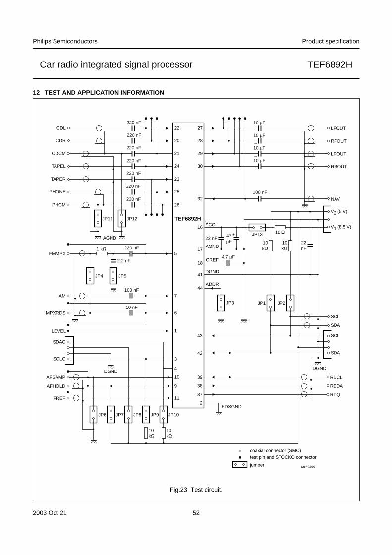
2003 Oct 21 52
Philips Semiconductors Product specification
Car radio integrated signal processor TEF6892H
12 TEST AND APPLICATION INFORMATION
handbook, full pagewidth 220 nF 10 µF
10 µF
10 µF
10 µF
100 nF
22 nF22nF
47µF
4.7 µF
22
20
21
24
27
28
29
30
32
16
17
18
23
25
26
CDL
CDR
CDCM
TAPEL
TAPER
PHONE
PHCM
FMMPX
220 nF
220 nF
220 nF
220 nF
TEF6892H
220 nF
220 nF
220 nF
100 nF
2.2 nF
AGND
DGND
JP12JP11
RFOUT
LFOUT
LROUT
RROUT
AM
5
7
NAV
SCL
SCL
SDA
SDA
V2 (5 V)
V1 (8.5 V)
10 nFMPXRDS
LEVEL
SDAG
SCLG
AFSAMP
AFHOLD
FREF
6
1
3
4
10
9
11RDQ
jumper
test pin and STOCKO connectorcoaxial connector (SMC)
MHC355
37
2
RDDA38
RDCL39
42
43
JP5JP4
JP6 JP7 JP8 JP9
10kΩ
1 kΩ
10kΩ
10kΩ
10kΩ
10 Ω
JP10
JP13
AGND
CREF
41
44
DGND
DGND
ADDR
RDSGND
VCC
JP1 JP2JP3
Fig.23 Test circuit.
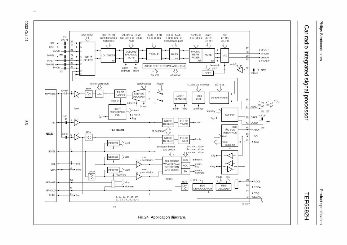
2003O
ct2153
Philips S
emiconductors
Product specification
Car radio integrated signal processor
TE
F6892H
This text is here in white to force landscape pages to be rotated correctly when browsing through the pdf in the Acrobat reader.This text is here in_white to force landscape pages to be rotated correctly when browsing through the pdf in the Acrobat reader.This text is here inThis text is here inwhite to force landscape pages to be rotated correctly when browsing through the pdf in the Acrobat reader. white to force landscape pages to be ...
hand
book
, ful
l pag
ewid
th
NOISEDETECT
NOISEBLANKER
PILOTCANCEL
INPUTSELECT
25
26
5
23
24
21
20
22CDL
7 ×220 nF
220 nF
100nF
10 nF
CDR
CDCM
TAPEL
TAPER
PHONEPHCM
7AM
NICE 6
MPXRDS
1LEVEL
3
4
SCL
SDA
10
i.c.
8, 12, 13, 14, 15, 19,31, 33, 34, 35, 36, 40
AFSAMP
9AFHOLD 37
38
39
2 RDSGND
MHC357
RDQ
RDDA
RDCL
42SDA
43SCL
++
+++
++
−
−
PILOT/REFERENCE
PLL
STEREODECODER HIGH
CUT
f: 1.5 to 15 kHz/widestereo adjustroll-off correction fm/am
NOISEDETECT
nb sensitivity
usnsensitivity
level
detection timingsand control
usn
sclg
11FREF fref
sdag
USN
MPX
snc start, slopehcc start, slopesm start, slope
MULTIPATH/WEAK SIGNAL
DETECTIONAND LOGIC
SNC
HCC
DETECT
SM
hold
RDSDEMODULATOR
57 kHz
sclg
writeautogate
I2C-BUSINTERFACE
SUPPLY
read
addr
sdag
RDS
PULSETIMER
TEF6892H
PULSETIMER
amnb
amnbfmsnc
amfm-softmute
afu-mute
asiasi
asi time asi active
level/offpitch
on/off
asi
fmnb amfmhcc
fmnb
fmsnc
amfm-hcc
wamsensitivity
amfm-softmute
LOUDNESS
input select 0 to −20 dBlow f: 50/100 Hz
high boost
DE-EMPHASIS
50/75 µs
Vref
standby
44ADDR
41 DGND
18 CREF
17 AGND
22nF
47µF
4.7 µF
16 VCC
32NAV
100 nF
30RROUT
29LROUT
28RFOUT
27LFOUT
DETECT
wamWAM
afus
reset/hold
afumute
Ireffref
TREBLE
AUDIO STEP INTERPOLATION (asi)
BEEP
+14 to −14 dBf: 8 to 15 kHz
+14 to −14 dBf: 60 to 120 Hz
shelve/band-pass
BASS
asi asi
front/rear0 to −59 dB
FRONT/REARFADER
mute:LF, RF,LR, RR
mix:LF, RF,LR, RR
MUTE MIX
VOLUME/BALANCE/
MUTE
vol: +20 to −59 dBbal: L/R, 0 to −79 dB
mute
57 kHz
38 kHz19 kHz
stereo
DETECT
level
mode rds
RDSDECODER
Fig.24 Application diagram.

2003 Oct 21 54
Philips Semiconductors Product specification
Car radio integrated signal processor TEF6892H
13 PACKAGE OUTLINE
UNIT A1 A2 A3 bp c E(1) e HE L L p Zywv θ
REFERENCESOUTLINEVERSION
EUROPEANPROJECTION ISSUE DATE
IEC JEDEC JEITA
mm 0.250.05
1.851.65 0.25
0.40.2
0.250.14
10.19.9 0.8 1.3
12.912.3
1.20.8
100
o
o0.15 0.10.15
DIMENSIONS (mm are the original dimensions)
Note
1. Plastic or metal protrusions of 0.25 mm maximum per side are not included.
0.950.55
SOT307-297-08-0103-02-25
D(1) (1)(1)
10.19.9
HD
12.912.3
EZ
1.20.8
D
e
E
B
11
c
EH
D
ZD
A
ZE
e
v M A
X
1
44
34
33 23
22
12
y
θ
A1A
Lp
detail X
L
(A )3A2
pin 1 index
DH v M B
bp
bp
w M
w M
0 2.5 5 mm
scale
QFP44: plastic quad flat package; 44 leads (lead length 1.3 mm); body 10 x 10 x 1.75 mm SOT307-2
Amax.
2.1
2003 Oct 21 55
Philips Semiconductors Product specification
Car radio integrated signal processor TEF6892H
14 SOLDERING
14.1 Introduction to soldering surface mountpackages
This text gives a very brief insight to a complex technology.A more in-depth account of soldering ICs can be found inour “Data Handbook IC26; Integrated Circuit Packages”(document order number 9398 652 90011).
There is no soldering method that is ideal for all surfacemount IC packages. Wave soldering can still be used forcertain surface mount ICs, but it is not suitable for fine pitchSMDs. In these situations reflow soldering isrecommended.
14.2 Reflow soldering
Reflow soldering requires solder paste (a suspension offine solder particles, flux and binding agent) to be appliedto the printed-circuit board by screen printing, stencilling orpressure-syringe dispensing before package placement.Driven by legislation and environmental forces theworldwide use of lead-free solder pastes is increasing.
Several methods exist for reflowing; for example,convection or convection/infrared heating in a conveyortype oven. Throughput times (preheating, soldering andcooling) vary between 100 and 200 seconds dependingon heating method.
Typical reflow peak temperatures range from215 to 270 °C depending on solder paste material. Thetop-surface temperature of the packages shouldpreferably be kept:
• below 225 °C (SnPb process) or below 245 °C (Pb-freeprocess)
– for all BGA and SSOP-T packages
– for packages with a thickness ≥ 2.5 mm
– for packages with a thickness < 2.5 mm and avolume ≥ 350 mm3 so called thick/large packages.
• below 240 °C (SnPb process) or below 260 °C (Pb-freeprocess) for packages with a thickness < 2.5 mm and avolume < 350 mm3 so called small/thin packages.
Moisture sensitivity precautions, as indicated on packing,must be respected at all times.
14.3 Wave soldering
Conventional single wave soldering is not recommendedfor surface mount devices (SMDs) or printed-circuit boardswith a high component density, as solder bridging andnon-wetting can present major problems.
To overcome these problems the double-wave solderingmethod was specifically developed.
If wave soldering is used the following conditions must beobserved for optimal results:
• Use a double-wave soldering method comprising aturbulent wave with high upward pressure followed by asmooth laminar wave.
• For packages with leads on two sides and a pitch (e):
– larger than or equal to 1.27 mm, the footprintlongitudinal axis is preferred to be parallel to thetransport direction of the printed-circuit board;
– smaller than 1.27 mm, the footprint longitudinal axismust be parallel to the transport direction of theprinted-circuit board.
The footprint must incorporate solder thieves at thedownstream end.
• For packages with leads on four sides, the footprint mustbe placed at a 45° angle to the transport direction of theprinted-circuit board. The footprint must incorporatesolder thieves downstream and at the side corners.
During placement and before soldering, the package mustbe fixed with a droplet of adhesive. The adhesive can beapplied by screen printing, pin transfer or syringedispensing. The package can be soldered after theadhesive is cured.
Typical dwell time of the leads in the wave ranges from3 to 4 seconds at 250 °C or 265 °C, depending on soldermaterial applied, SnPb or Pb-free respectively.
A mildly-activated flux will eliminate the need for removalof corrosive residues in most applications.
14.4 Manual soldering
Fix the component by first soldering twodiagonally-opposite end leads. Use a low voltage (24 V orless) soldering iron applied to the flat part of the lead.Contact time must be limited to 10 seconds at up to300 °C.
When using a dedicated tool, all other leads can besoldered in one operation within 2 to 5 seconds between270 and 320 °C.

2003 Oct 21 56
Philips Semiconductors Product specification
Car radio integrated signal processor TEF6892H
14.5 Suitability of surface mount IC packages for wave and reflow soldering methods
Notes
1. For more detailed information on the BGA packages refer to the “(LF)BGA Application Note” (AN01026); order a copyfrom your Philips Semiconductors sales office.
2. All surface mount (SMD) packages are moisture sensitive. Depending upon the moisture content, the maximumtemperature (with respect to time) and body size of the package, there is a risk that internal or external packagecracks may occur due to vaporization of the moisture in them (the so called popcorn effect). For details, refer to theDrypack information in the “Data Handbook IC26; Integrated Circuit Packages; Section: Packing Methods”.
3. These transparent plastic packages are extremely sensitive to reflow soldering conditions and must on no accountbe processed through more than one soldering cycle or subjected to infrared reflow soldering with peak temperatureexceeding 217 °C ± 10 °C measured in the atmosphere of the reflow oven. The package body peak temperaturemust be kept as low as possible.
4. These packages are not suitable for wave soldering. On versions with the heatsink on the bottom side, the soldercannot penetrate between the printed-circuit board and the heatsink. On versions with the heatsink on the top side,the solder might be deposited on the heatsink surface.
5. If wave soldering is considered, then the package must be placed at a 45° angle to the solder wave direction.The package footprint must incorporate solder thieves downstream and at the side corners.
6. Wave soldering is suitable for LQFP, TQFP and QFP packages with a pitch (e) larger than 0.8 mm; it is definitely notsuitable for packages with a pitch (e) equal to or smaller than 0.65 mm.
7. Wave soldering is suitable for SSOP, TSSOP, VSO and VSSOP packages with a pitch (e) equal to or larger than0.65 mm; it is definitely not suitable for packages with a pitch (e) equal to or smaller than 0.5 mm.
8. Hot bar or manual soldering is suitable for PMFP packages.
PACKAGE (1)SOLDERING METHOD
WAVE REFLOW (2)
BGA, LBGA, LFBGA, SQFP, SSOP-T(3), TFBGA, VFBGA not suitable suitable
DHVQFN, HBCC, HBGA, HLQFP, HSQFP, HSOP, HTQFP,HTSSOP, HVQFN, HVSON, SMS
not suitable(4) suitable
PLCC(5), SO, SOJ suitable suitable
LQFP, QFP, TQFP not recommended(5)(6) suitable
SSOP, TSSOP, VSO, VSSOP not recommended(7) suitable
PMFP(8) not suitable not suitable

2003 Oct 21 57
Philips Semiconductors Product specification
Car radio integrated signal processor TEF6892H
15 DATA SHEET STATUS
Notes
1. Please consult the most recently issued data sheet before initiating or completing a design.
2. The product status of the device(s) described in this data sheet may have changed since this data sheet waspublished. The latest information is available on the Internet at URL http://www.semiconductors.philips.com.
3. For data sheets describing multiple type numbers, the highest-level product status determines the data sheet status.
LEVELDATA SHEET
STATUS(1)PRODUCT
STATUS(2)(3) DEFINITION
I Objective data Development This data sheet contains data from the objective specification for productdevelopment. Philips Semiconductors reserves the right to change thespecification in any manner without notice.
II Preliminary data Qualification This data sheet contains data from the preliminary specification.Supplementary data will be published at a later date. PhilipsSemiconductors reserves the right to change the specification withoutnotice, in order to improve the design and supply the best possibleproduct.
III Product data Production This data sheet contains data from the product specification. PhilipsSemiconductors reserves the right to make changes at any time in orderto improve the design, manufacturing and supply. Relevant changes willbe communicated via a Customer Product/Process Change Notification(CPCN).
16 DEFINITIONS
Short-form specification The data in a short-formspecification is extracted from a full data sheet with thesame type number and title. For detailed information seethe relevant data sheet or data handbook.
Limiting values definition Limiting values given are inaccordance with the Absolute Maximum Rating System(IEC 60134). Stress above one or more of the limitingvalues may cause permanent damage to the device.These are stress ratings only and operation of the deviceat these or at any other conditions above those given in theCharacteristics sections of the specification is not implied.Exposure to limiting values for extended periods mayaffect device reliability.
Application information Applications that aredescribed herein for any of these products are forillustrative purposes only. Philips Semiconductors makeno representation or warranty that such applications will besuitable for the specified use without further testing ormodification.
17 DISCLAIMERS
Life support applications These products are notdesigned for use in life support appliances, devices, orsystems where malfunction of these products canreasonably be expected to result in personal injury. PhilipsSemiconductors customers using or selling these productsfor use in such applications do so at their own risk andagree to fully indemnify Philips Semiconductors for anydamages resulting from such application.
Right to make changes Philips Semiconductorsreserves the right to make changes in the products -including circuits, standard cells, and/or software -described or contained herein in order to improve designand/or performance. When the product is in full production(status ‘Production’), relevant changes will becommunicated via a Customer Product/Process ChangeNotification (CPCN). Philips Semiconductors assumes noresponsibility or liability for the use of any of theseproducts, conveys no licence or title under any patent,copyright, or mask work right to these products, andmakes no representations or warranties that theseproducts are free from patent, copyright, or mask workright infringement, unless otherwise specified.
2003 Oct 21 58
Philips Semiconductors Product specification
Car radio integrated signal processor TEF6892H
18 PURCHASE OF PHILIPS I2C COMPONENTS
Purchase of Philips I2C components conveys a license under the Philips’ I2C patent to use thecomponents in the I2C system provided the system conforms to the I2C specification defined byPhilips. This specification can be ordered using the code 9398 393 40011.

© Koninklijke Philips Electronics N.V. 2003 SCA75All rights are reserved. Reproduction in whole or in part is prohibited without the prior written consent of the copyright owner.
The information presented in this document does not form part of any quotation or contract, is believed to be accurate and reliable and may be changedwithout notice. No liability will be accepted by the publisher for any consequence of its use. Publication thereof does not convey nor imply any licenseunder patent- or other industrial or intellectual property rights.
Philips Semiconductors – a worldwide company
Contact information
For additional information please visit http://www.semiconductors.philips.com . Fax: +31 40 27 24825For sales offices addresses send e-mail to: [email protected] .
Printed in The Netherlands 753503/01/pp59 Date of release: 2003 Oct 21 Document order number: 9397 750 10355


