+ All Categories
Home > Documents > TELEVISOR A LCD MANUAL DE...

TELEVISOR A LCD MANUAL DE...

Date post: 27-May-2018
Category:
Upload: vuongxuyen
View: 223 times
Download: 0 times
Share this document with a friend
42
TELEVISOR A LCD MANUAL DE SERVICIO ATENCIÓN Antes de dar servicio al chasis, lea las PRECAUCIONES DE SEGURIDAD en este manual. CHASIS : LP78B MODELO : 37LC4R 37LC4R-MD website:http://biz.LGservice.com Internal Use Only
Transcript

TELEVISOR A LCDMANUAL DE SERVICIO

ATENCIÓNAntes de dar servicio al chasis, lea las PRECAUCIONES DE SEGURIDADen este manual.

CHASIS : LP78B

MODELO : 37LC4R 37LC4R-MD

website:http://biz.LGservice.com

R

Internal Use Only

- 2 -Copyright 2007 LG Electronics. Inc. All right reserved.Only for training and service purposes

LGE Internal Use Only

CONTENIDO

CONTENIDO ............................................................................................ 2

PRECAUCIONES DE SEGURIDAD ..........................................................3

ESPECIFICACIONES ...............................................................................4

INSTRUCCIÓN DE AJUSTE .....................................................................8

SOLUCIÓN DE PROBLEMAS.................................................................19

DIAGRAMA EN BLOQUE .......................................................................27

VISTA EN DESPIECE ............................................................................ 29

LISTA DE PARTES DE REPUESTOS .................................................... 31

PAGINA DE SVC ........................................................................................

- 3 -Copyright 2007 LG Electronics. Inc. All right reserved.Only for training and service purposes

LGE Internal Use Only

PRECAUCIONES DE SEGURIDAD

ADVERTENCIA: Antes de dar servicio a este chasis, lea "PRECAUCIONES RESPECTO A RADIACION POR RAYOS X","INSTRUCCIONES DE SEGURIDAD" y "AVISO SOBRE SEGURIDAD DE PRODUCTOS"

Muchas de las partes, electricas y mecánicas en este chasis tienen caracteristicas relacionadas con la seguridad. Estascaracteristicas frecuentemente pasan desapercibidas en las inspecciones visuales y la proteccion que proporcionan contra laRADIACION DE RAYOS-X no siempre necesariamente se obtiene al mismo grado cuando se reemplazan piezas o componentesdiseñados para voltajes o vatajes mayores, etc. Las piezas que tienen estas caracteristicas de seguridad se identifican por lamarca impresa sobre el diagrama esquematico y la marca impresa en la lista de partes. Antes de reemplazar alguno deesos componente, lea cuidadosamente la lista de este manual. El uso de partes de reemplazo que no tengan las mismascaracteristicas de seguridad, como se especifica en la lista de partes, puede crear Radiacion de Rayos-X.

1. Cuando el receptor está en operación, se producen voltajespotencialmente tan altos como 25,000-29,000 voltios. Operarel receptor fuera de su gabinete o con la tapa traseraremovida puede causar peligro de choque eléctrico.(1)Nadie debe intentar dar servicio si no está debidamente

familiarizado con las precauciones que son necesariascuando se trabaja con un equipo de alto voltaje.

(2)Siempre descargue el ánodo del tubo de la imagen a tierrapara evitar el riesgo de choque eléctrico antes de removerla tapa del ánodo.

(3)Descargue completamente el alto potencial del tubo deimagen antes de manipularlo. El tubo de la imagen es dealto vacío y, si se rompe, los fragmentos de vidrio salendespedidos violentamente.

2. Si se quemara algún fusible de este receptor de televisión,reemplácelo con otro especificado en la lista de partes.

3. Cuando reemplace tableros o plaquetas de circuitos,cuidadosamente enrolle sus alambres alrededor de lasterminales antes de soldar.

4. Cuando reemplace un resistencia de vataje (resistor depelícula de óxido metálico) en el Tablero o Plaqueta decircuitos, mantenga la resistencia a un mínimo de 10mm dedistancia.

5. Mantenga los alambres lejos de componentes de alto voltajeo de alta temperatura.

6. Este receptor de televisión debe conectarse a una fuente de100 a 240 V AC.

7. Antes de devolver este aparato al cl iente, haga unaverificación de fuga de corriente sobre las partes metálicasdel gabinete expuestas, tales como antenas, terminales,cabezas de tornillos, tapas de metal, palancas de control etc.,para estar seguro de que el equipo funciona sin peligro dechoque eléctrico. Enchufe el cordón directamente altomacorriente de la línea de AC 100-240V.

No utilice una línea aislada de transformador durante estaverificación. Use un voltímetro de 1000 Ohmios por voltiode sensibilidad o más, en la forma que se describe acontinuación.Cuando la unidad está ya conectada a la AC, pulse elconmutador primero poniéndolo en "ON" (encendiendo) yluego en "OFF" (apagando), mida desde un punto de tierraconocido, tal como una (cañería de metal, una manijametálica, una tubería etc.) a todas las partes metálicasexpuestas del receptor de televisión (antenas, manijas demetal, gabinetes de metal, cubiertas de metal, palancas decontrol etc.,) especialmente cualquiera de las partesmetálicas expuestas que puedan ofrecer un camino hacia elchasis. Ninguna medición de corriente eléctrica debe excederde 0.5 miliamperios. Repita la prueba cambiando la posicióndel enchufe en el tomacorriente. Cualquier medición que noesté dentro de los límites especificados aquí representan unriesgo potencial de choque eléctrico que debe ser eliminadoantes de devolver el equipo al cliente.

INSTRUCCIONES DE SEGURIDAD

AVISO SOBRE SEGURIDAD DE PRODUCTOS

DEVICEUNDERTEST

TEST ALLEXPOSED METAL

SURFACES

2- WIRE CORD

ALSO TEST WITHPLUG REVERSED(USING A C ADAPTERPLUG AS REQUIRED)

EARTHGROUND

LEAKAGECURRENTTESTER

(READING SHOULDNOT BE ABOVE

0.5mA)

Aparatobajoexamen

Probadorde fuga decorriente

La lectura no debeexceder de 0.5mA

Pruebe todaslas superficiesmetálicas

Tambien pruebe cónlos enchufes al reves(utilizando adaptadoren caso necesario)

Tierrasuelo

- 4 -Copyright 2007 LG Electronics. Inc. All right reserved.Only for training and service purposes

LGE Internal Use Only

1. Rango de aplicaciónEsta hoja de especificaciones es aplicada a la TV LCD queutiliza la carcasa LP78B.

2. EspecificaciónCada pieza se somete a una serie de pruebas como lassiguientes sin necesidad de solicitar citas especiales.

(1) Temperatura : 25±5º (77±9º), CST : 40±5º(2) 2.2 Humedad relativa : 65±10%(3) Potencia/Voltaje : voltaje de entrada estándar (100~240 V

a 50/60 Hz)* El voltaje estándar de cada producto está marcado por

modelos.(4) La especificación y rendimiento de cada una de las piezas

puede seguirse en cada dibujo y especificación pornúmero de pieza conforme a BOM.

(5) El receptor debe ser operado durante aproximadamente20 minutos antes del ajuste.

3. Método de prueba(1) Rendimiento : se ha seguido el método de prueba de la

TV LGE.(2) Se demanda otra especificación

Seguridad : Especificación CE, IECEMC : CE, IEC

ESPECIFICACIONESNOTA: las especificaciones que reflejan mejoras en los productos están sujetos a cambios sin previo aviso.

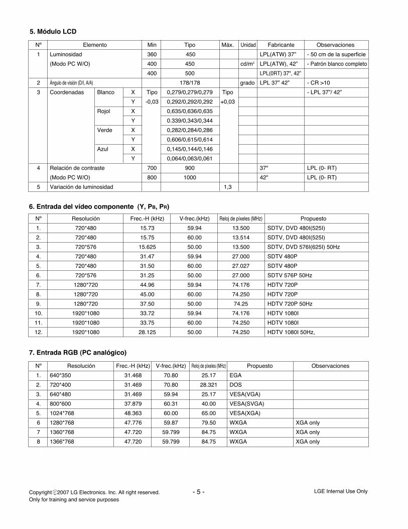
4. Especificación general (MÓDULO LCD DE 26/27/32/37/42”)

Nº Elemento Especificación Medidas Resultado Observaciones

1 Dispositivo de Módulo de visualización en LCD

visualización en pantalla color de 37/42"

2 Proporción de aspecto 16 : 9

3 Módulo LCD LCD TFT WXGA de 37/42 pulg. FABRICANTE: AUO/CMO/LPL/CPT

4 Entorno operativo 1) Temp. : 0 ~ 40ºC ESPEC. LGE

2) Humedad : 0 ~ 85%

5 Entorno de 1) Temp. : -20 ~ 60ºC

almacenamiento 2) Humedad : 0 ~ 85%

6 Tensión de entrada 100 ~ 240 V de CA, 50/60 Hz

7 Consumo de potencia Encendido (verde) Volumen: 1/8 volumen del

≤ TBD (42”) punto de distorsión del

≤ máx. (37”) sonido

En espera (rojo) : 1,0 W

8 Módulo LCD AUO Dimensiones 37” 877.0 x 514.6 x 54.7 mm (A) x (V) x (P)[con inversor]

exteriores

Separación entre 37” 0.6 x 0.6 mm

píxeles

Luz de fondo 37” 10 luces U

LPL Contorno 37” 877.0 x 516.8 x 55.5 mm (A) x (V) x (P) [con inversor]

Dimensión 42” 1006 x 610 x 56

Separación entre 37” 0.200 x 0.600 mm

píxeles 42” 0.227 x 0.681

Luz de fondo 37” 20 EEFL (LC260WX2-SLB3)

42” 20 CCFL

Colores en pantalla 16,7M (16,777,216) (LPL 26”)

Revestimiento 3H,AG

- 5 -Copyright 2007 LG Electronics. Inc. All right reserved.Only for training and service purposes

LGE Internal Use Only

5. Módulo LCD

6. Entrada del vídeo componente (Y, PB, PR)

7. Entrada RGB (PC analógico)

Nº Elemento Min Tipo Máx. Unidad Fabricante Observaciones

1 Luminosidad 360 450 LPL(ATW) 37” - 50 cm de la superficie

(Modo PC W/O) 400 450 cd/m2 LPL(ATW), 42” - Patrón blanco completo

400 500 LPL(0RT) 37", 42”

2 Ángulo de visión (D/I, A/A) 178/178 grado LPL 37” 42” - CR >10

3 Coordenadas Blanco X Tipo 0,279/0,279/0,279 Tipo - LPL 37”/ 42”

Y -0,03 0,292/0,292/0,292 +0,03

Rojol X 0,635/0,636/0,635

Y 0.339/0,343/0,344

Verde X 0,282/0,284/0,286

Y 0,606/0,615/0,614

Azul X 0,145/0,144/0,146

Y 0,064/0,063/0,061

4 Relación de contraste 700 900 37" LPL (0- RT)

(Modo PC W/O) 800 1000 42" LPL (0- RT)

5 Variación de luminosidad 1,3

Nº Resolución Frec.-H (kHz) V-frec.(kHz) Reloj de píxeles (MHz) Propuesto

1. 720*480 15.73 59.94 13.500 SDTV, DVD 480I(525I)

2. 720*480 15.75 60.00 13.514 SDTV, DVD 480I(525I)

3. 720*576 15.625 50.00 13.500 SDTV, DVD 576I(625I) 50Hz

4. 720*480 31.47 59.94 27.000 SDTV 480P

5. 720*480 31.50 60.00 27.027 SDTV 480P

6. 720*576 31.25 50.00 27.000 SDTV 576P 50Hz

7. 1280*720 44.96 59.94 74.176 HDTV 720P

8. 1280*720 45.00 60.00 74.250 HDTV 720P

9. 1280*720 37.50 50.00 74.25 HDTV 720P 50Hz

10. 1920*1080 33.72 59.94 74.176 HDTV 1080I

11. 1920*1080 33.75 60.00 74.250 HDTV 1080I

12. 1920*1080 28.125 50.00 74.250 HDTV 1080I 50Hz,

Nº Resolución Frec.-H (kHz) V-frec.(kHz) Reloj de píxeles (MHz) Propuesto Observaciones

1. 640*350 31.468 70.80 25.17 EGA

2. 720*400 31.469 70.80 28.321 DOS

3. 640*480 31.469 59.94 25.17 VESA(VGA)

4. 800*600 37.879 60.31 40.00 VESA(SVGA)

5. 1024*768 48.363 60.00 65.00 VESA(XGA)

6 1280*768 47.776 59.87 79.50 WXGA XGA only

7 1360*768 47.720 59.799 84.75 WXGA XGA only

8 1366*768 47.720 59.799 84.75 WXGA XGA only

- 6 -Copyright 2007 LG Electronics. Inc. All right reserved.Only for training and service purposes

LGE Internal Use Only

8. Entrada HDMI (DTV)

Nº Resolución Frec.-H (kHz) V-frec.(kHz) Reloj de píxeles (MHz) Propuesto Observaciones

1 720*480 15.75 60.00 13.514 SDTV, DVD 480I(525I) support(not spec)

2 720*480 15.73 59.94 13.500 SDTV, DVD 480I(525I) support(not spec)

3 720*576 15.625 50.00 13.500 SDTV, DVD 576I(625I) 50Hz support(not spec)

4 720*480 31.47 59.94 27.000 SDTV 480P

5 720*480 31.50 60.00 27.027 SDTV 480P

6 720*576 31.25 50.00 27.000 SDTV 576P 50Hz

7 1280*720 44.96 59.94 74.176 HDTV 720P

8 1280*720 45.00 60.00 74.250 HDTV 720P

9 1280*720 37.50 50.00 74.25 HDTV 720P 50Hz

10 1920*1080 33.72 59.94 74.176 HDTV 1080I

11 1920*1080 33.75 60.00 74.250 HDTV 1080I

12 1920*1080 28.125 50.00 74.250 HDTV 1080I 50Hz

13 1920*1080 67.432 59.94 148.350 HDTV 1080P

14 1920*1080 67.5 60 148.5 HDTV 1080P

15 1920*1080 56.250 50 148.5 HDTV 1080P 50Hz

- 7 -Copyright 2007 LG Electronics. Inc. All right reserved.Only for training and service purposes

LGE Internal Use Only

10. Especificación mecánica

Nº Elemento Ajustes Observaciones

1. CONFIGUR ACIÓN Sintonización automática: Para iniciar

Sintonización manual TV 2

Memoria ACT.

Bien

Canal preferido -- -----

2. Imagen Modo de imagen Dinámica

Temperatura de color desactivar

XD Automático

Avanzada Cine : Apagado

Nivel de negro : bajo (MODO HDMI)

alto (MODO AV)

Proporción de aspecto 16: 9

Reinic. imagen Para establecer

Pantalla Para establecer

XD Demo Para iniciar

3. Sonido Modo sonido Estándar

Volumen autom. Apagado

Balance 0

Altavoz Encendido

4. Horas Reloj --: --

Tiempo apagado --: --

Apagado

Tiempo encendido --: --

Can. TV2

Vol. 30

Apagado

Apagado automático Apagado

Apagado automático Apagado

5. OPCIÓN Idioma Inglés Conforme a demanda del cliente, PR

Subtítulos/Texto Apagado

SIMPLINK Encendido

Bloqueo de controles Apagado

9. Condición de fábrica SET

Nº Elemento Content Observaciones

1. Producto Anchura Longitud Altura Unidad

Dimensión Previo al embalaje 926.6 280.4 697.6 mm EQUIPO (con soporte)

Tras el embalaje 999 264 874 mm

2. Producto Peso Sólo el EQUIPO 20

Con CAJA 16.3

- 8 -Copyright 2007 LG Electronics. Inc. All right reserved.Only for training and service purposes

LGE Internal Use Only

INSTRUCCIÓN DE AJUSTE

1. Rango de aplicación

Esta hoja de especificaciones es aplicable a todas las TV(PP78A/B) PDD de 42/50 pulgadas y TV (LP78A/B) LCD de26/32/37/42 pulgadas fabricadas en plantas LG de TV detodo el mundo.

2. Especificación

1) El aislamiento de este chasis no es del tipo de carga y noes necesario usar el transformador de aislamiento. Sinembargo, el uso de un transformador de aislamiento leayudará a proteger los instrumentos de pruebas.

2) Los ajustes deben realizarse en el orden correcto.3) Los ajustes deben efectuarse bajo condiciones de 25±5° C

de temperatura y un 65±10% de humedad relativa, si noexisten más designaciones específicas.

4) La tensión de entrada del receptor debe mantenersedentro del rango de 100~220 V, 50/60 Hz.

5) Antes de realizar los ajustes, active el funcionamientodurante 30 minutos.

3. Elementos de ajuste

3.1. Elementos de ajuste del montaje de laPCI

1) Descargue el software principal VCTP (IC500,VCT_Pro)2) Memoria de canales (IC501,EEPROM)3) Ajuste de la portadora de color

3.2. Elementos de ajuste del montaje delEQUIPO

1) Entrada de datos DDC2) Ajuste de balance de blancos3) Comparar entrada de datos opcional

4. Método de ajuste del montaje de laPCI

4.1. Descargar instalación del programa(1) Extraer un archivo Zip

(2) Instalación del controlador Visual I2C y LPT

(3) Verificação (Iniciar > Programas > Micronas > Visual I2Cou LptDrv)

(4) Ajuste del retardo LPT (Archivo > Preferencia >Preferencias LPT..)

Inste el controlador LPTInstale el controladorVisual I2C

*LPT SETTING- Delay => 1- Time out => 500 ms

- 9 -Copyright 2007 LG Electronics. Inc. All right reserved.Only for training and service purposes

LGE Internal Use Only

(5) Intercambie el archivo bootloader.bat

=> Seleccione el archivo "bootloader.bat" (instalar > VCTP_download > bootloader)

=> Presione "OK"=> Finalice el programa, tras guardar el archivo

"download_cs.vi2c"(Si hace clic en , el mensaje aparecerá automáticamente)

4.2. Descarga del programa de SW(1) Perfil : para la descarga del software a la

memoria flash del vctp (IC500)(2) Equipamiento

1) PC2) Programa Visual IIC 3) Adaptador de descarga

(3) Estructura de conexión

(4) Estado de conexión1) Nombre IC y número de circuito: VCTp y IC5002) Tensión de uso: 3,3 V (5 clavijas)3) SCL : 15 clavijas4) SDA : 12 clavijas5) Tiempo de tac.: aprox. 1 minuto y 20 segundos

(5) Método de descarga1) Método de descarga1 (montaje de la PCI)

(A) Conecte el adaptador de descarga de la toma D-sub(B) Ejecute el programa ‘Download.vi2c’ en el PC,

mediante el que se abrirá una ventana principal

x

PC

Download jig

RGB cable

Main

B/D

- 10 -Copyright 2007 LG Electronics. Inc. All right reserved.Only for training and service purposes

LGE Internal Use Only

(C) Haga doble clic en el cuadro rojo y confirme que la"Versión del Bootloader" es la 42.

(D) Haga clic en el botón "Borrar Flash"

(E) Haga doble clic en el archivo descargado y se abrirá laventana "editar".

(F) Haga clic en el botón de selección de la "ventanaeditar"; a continuación se abrirá la "ventana selecciónde archivo"

(G) Seleccione el archivo Hex en la carpeta y ejecute ladescarga haciendo clic en el botón "abrir".

(H) Haga clic en el botón OK en la "ventana editar"(I) Bajo el proceso de descarga

(J) Si la descarga falla, por ejemplo "Sin reconocimientodel equipo esclavo", ejecute de nuevo la descargaen (1)

2) Método de descarga 2 (montaje de la placa AV)

(A) Presione S/W ‘ON" (conecte SCL a GND mediante elinterruptor en el adaptador) y conecte el adaptador dedescarga a la toma D-sub

Push S/W

- 11 -Copyright 2007 LG Electronics. Inc. All right reserved.Only for training and service purposes

LGE Internal Use Only

(B) Active el suministro de potencia (en espera 5 V) yespere 3 segundos

(C) Presione el S/W ‘OFF’ (desconecte el SCL de GNDmediante el interruptor en el adaptador)

(D) Ejecute el programa ‘Download.vi2c’ en el PC,mediante el que se abrirá una ventana principal

(E) Haga doble clic en el cuadro azul y confirme que la"Versión del Bootloader" es la 42.

(F) Haga clic en el botón "Borrar Flash"

(G) Haga doble clic en el archivo descargado y se abrirá laventana "editar".

(H) Haga clic en el botón de selección de la "ventanaeditar"; a continuación se abrirá la "ventana selecciónde archivo".

(I) Seleccione el archivo Hex en la carpeta y ejecute ladescarga haciendo clic en el botón "abrir".

Push S/W

- 12 -Copyright 2007 LG Electronics. Inc. All right reserved.Only for training and service purposes

LGE Internal Use Only

(J) Haga clic en el botón OK en la "ventana editar"

(K) Descargando

(L) Si la descarga falla, por ejemplo "Sin reconocimientodel equipo esclavo", ejecute de nuevo la descargaen (1)

3) Método de descarga 3 (EQUIPO)(A) Presione el botón "Tilt" y ajuste el mando a distancia;

después el PDP cambiará al "modo esclavo"

(B) Conecte el adaptador a la TV mediante un cable D-sub

(C) Ejecute el programa ‘Download_CS.vi2c’ en el PC,mediante el que se abrirá una ventana principal.

(D) Haga clic en el botón "GO".

Si no presiona "GO", el archivo Hex no será descargado,pese a que la descarga continuará aparentemente deforma normal.

(E) Haga doble clic en el cuadro azul y confirme que la"Versión del Bootloader" es la 42.

(F) Haga clic en el botón "Borrar Flash"

(G) Haga doble clic en el archivo descargado y se abrirá laventana "editar".

- 13 -Copyright 2007 LG Electronics. Inc. All right reserved.Only for training and service purposes

LGE Internal Use Only

(H) Haga clic en el botón de selección de la "ventanaeditar"; a continuación se abrirá la "ventana selecciónde archivo"

(I) Seleccione el archivo Hex en la carpeta y ejecute ladescarga haciendo clic en el botón "abrir".

(J) Haga clic en el botón OK en la "ventana editar"

(K) bajo el proceso de descarga

(L) Si la descarga falla, por ejemplo "Sin reconocimientodel equipo esclavo", ejecute de nuevo la descargaen (1)

4.3. Descarga de la memoria de canales

(1) Perfil : para la descarga de la memoria de canales aEeprom (IC501), para comprobar el equipo sin problemasen la TV.

(2) Equipamiento1) PC2) Programa Visual IIC 3) Adaptador de descarga

(3) Estructura de conexión

(4) Estado de conexión1) Nombre IC y número de circuito: VCTp y IC5002) Tensión de uso: 3,3 V (5 clavijas)3) SCL : 15 clavijas4) SDA : 12 clavijas5) Tiempo de tac.: aprox. 3 segundos

(5) Método de transferência1) Ligue o dispositivo de transferência ao conector D-sub.2) `Execute o programa ‘Channel.vi2c’ no PC; será aberta

uma janela principal.

3) Presione el botón de cambio y seleccione los datos dela memoria de canales.

PC

Download jig

RGB cable

Main

B/D

- 14 -Copyright 2007 LG Electronics. Inc. All right reserved.Only for training and service purposes

LGE Internal Use Only

4) Compruebe si la comunicación es o no correcta.=> presione el área Lectura (Comprobación de reconoc.) y

compruebe que el mensaje OK aparece dentro del áreaazul.

.5) (5) Presione la opción Actualizar NVM en Archivo.

4.4. Opción HERRAMIENTAS, Cambio deopción de área

(1) Perfil: el valor de opción debe modificarse por si difiere dealgún valor de ajuste, dependiendo del módulo, pulgadasy mercado.

(2) Equipamiento: mando a distancia de ajuste (3) Método de ajuste

Antes de comprobar PCBA, es necesario cambiar losvalores opcionales de la opción Herramientas y Área acontinuación.

(De no modificar la opción, el menú de entrada podría diferirde las especificaciones del modelo)Los métodos de entrada son los mismos que otros equipos.(Utilice la tecla Ajuste en el mando a distancia).

4.5. Ajuste de la portadora de color(proceso de inspección)

(1) Perfil : para establecer el margen de desviación de laportadora de color dentro de las especificaciones.1) Equipamiento : mando a distancia de ajuste

Señal Pal RF2) Conexión : la TV debe conectarse a la señal Pal RF (EU

5CH)3) Método de ajustea Sintonizar la señal RF

ZB, TB : PAL Philips Pattern (con barra de colores)

b.Presione la tecla "adj" en el mando a distanciacorrespondiente.

4) Equipamiento: mando a distancia de ajuste Señal NTSC RF

5) Conexión : la TV debe conectarse a la señal NTSC RF(US 4CH)

6) Método de ajustea Sintonizar la señal RF

MD : NTSC - US 4CH

b Presione la tecla "adj" en el mando a distanciacorrespondiente.

- 15 -Copyright 2007 LG Electronics. Inc. All right reserved.Only for training and service purposes

LGE Internal Use Only

5. Método de ajuste del montaje delEQUIPO

* Precaución : Cada montaje de PCI debe comprobarsemediante Comprobar JIG(debido a posibles daños en el montaje de la PCIal módulo PDP, tenga especial cuidado)

5.1. Descarga EDID (datos ampliados deidentificación de pantalla)/DDC (canalde datos de pantalla)

(1) Perfil : a fin de permitir el método "plug-and-play"(2) Equipamiento

1) Ajuste del PC con S/W para la escritura de datos EDID.(S/W : EDID TESTER Ver.2.5)

2) Un adaptador para la descarga EDID3) Cable: cable D-sub de 15 clavijas, cable HDMI

(3) Estructura de conexión

Fig. 5 Diagrama de conexión de la descarga DDC

-> Precaución : - No conecte nunca la HDMI y el cable D-SUBal mismo tiempo.

- Uti l ice los cables adecuados, acontinuación, para la escritura EDID

(4) Preparación para el ajuste1) Como en la anterior Fig. 5, Conecte el equipo, el

adaptador de descarga EDID, el PC y el cable2) Encienda el PC y el adaptador de descarga EDID. Y

ejecue el S/W : EDID TESTER Ver.2.53) Configure la opción de S/W

Nº de repetición : 5Dirección del dispositivo : A0PageByte : 8

4) Encienda el equipo

(5) Secuencia de ajuste1) Datos DDC de RGB analógico1.1. Inicie los datos1.2. Suba los datos EDID. (Abrir archivo).

1.3. Configure el S/W como se detalla a continuación.

1.4. Presione el botón "Escribir datos y verificar". Yconfirme seleccionando "Sí".

[RGB analógico : L(P)P78A_RGB.ANA ][Digital – HDMI1: L(P)P78A_HDMI1.DVI ][Digital – HDMI2: L(P)P78A_HDMI2.DVI ]

For RGB EDID For HDMI EDID

- 16 -Copyright 2007 LG Electronics. Inc. All right reserved.Only for training and service purposes

LGE Internal Use Only

1.5. Si ha completado el proceso de escritura, podráobservar el mensaje "OK".

Fig. 6 DATOS EDID

(6) Datos EDID< Analógico (RGB) >

< Digital1 (HDMI/DVI 1) >

< Digital 2 (HDMI 2) >

< Analógico (RGB) >

< Digital1 (HDMI/DVI 1) >

< Digital 2 (HDMI 2) >

-> Las opciones de detalles EDID son las siguientes (

)

ID del producto

Nº de serie-> Controlado en la línea de producciónMes, año-> Controlado en la línea de producción:

Ej.) Mensualmente : ‘03’ -> ‘03’ Año : ‘2005’ -> ‘0F’

Nombre del modelo: nombre del modelo -> LG TV

LG TV

Suma de verificación (7EH)-> Modificable mediante el total de datos EDID

ⓐ ⓑ

Addr 00 01 02 03 04 05 06 07 08 09 0A 0B 0C 0D 0E 0F

0000 00 F F F F F F F F F F F F 00 1E 6D

0010 01 03 08 46 27 78 0A D9 B0 A3 57 49 9C 25

0020 11 49 4B A1 08 00 31 40 01 01 01 01 45 40 01 01

0030 61 40 01 01 01 01 1B 21 50 A0 51 00 1E 30 48 88

0040 35 00 BC 88 21 00 00 1C 4E 1F 00 80 51 00 1E 30

0050 40 80 37 00 BC 88 21 00 00 18 00 00 00 FD 00 3A

0060 3F 1F 32 09 00 0A 20 20 20 20 20 20

0070 00

Addr 00 01 02 03 04 05 06 07 08 09 0A 0B 0C 0D 0E 0F

0000 00 F F F F F F F F F F F F 00 1E 6D

0010 01 03 08 46 27 78 0A D9 B0 A3 57 49 9C 25

0020 11 49 4B A1 08 00 31 40 01 01 01 01 45 40 01 01

0030 61 40 01 01 01 01 D5 09 80 A0 20 E0 2 D 10 08 60

0040 22 00 98 06 32 08 08 18 64 19 00 40 41 00 26 30

0050 18 88 36 00 98 06 32 00 00 18 00 00 00 FD 00 3A

0060 3F 1F 32 09 00 0A 20 20 20 20 20 20

0070 00

ⓐ ⓑⓒ

ⓓⓓ ⓔ

Addr 00 01 02 03 04 05 06 07 08 09 0A 0B 0C 0D 0E 0F

0000 00 F F F F F F F F F F F F 00 1E 6D

0010 01 03 80 46 27 78 EA D9 B0 A3 57 49 9C 25

0020 11 49 4B 81 08 00 01 01 01 01 01 01 45 40 01 01

0030 61 40 01 01 01 01 D5 09 80 A0 20 E0 2D 10 08 60

0040 22 00 98 06 32 08 08 18 64 19 00 40 41 00 26 30

0050 18 88 36 00 98 06 32 00 00 18

0060 00 00 00 F D

0070 00 3A 3F 1F 32 09 00 0A 20 20 20 20 20 20 01

0080 02 03 20 F1 4D 01 06 07 15 16 02 03 11 12 13 04

0090 14 85 23 09 07 07 83 01 00 00 65 03 0C 00 0011110000

00A0 01 1D 00 80 51 D0 1C 20 40 80 35 00 BC 88 21 00

00B0 00 1E 8C 0A D0 8A 20 E0 2D 10 10 3E 96 00 13 8E

00C0 21 00 00 18 01 1D 80 18 71 1C 16 20 58 2C 25 00

00D0 C4 8E 21 00 00 9E 00 00 00 00 00 00 00 00 00 00

00E0 00 00 00 00 00 00 00 00 00 00 00 00 00 00 00 00

00F0 00 00 00 00 00 00 00 00 00 00 00 00 00 00 00

ⓐ ⓑⓒ

ⓓⓓ

Addr 00 01 02 03 04 05 06 07 08 09 0A 0B 0C 0D 0E 0F

0000 00 F F F F F F F F F F F F 00 1E 6D

0010 01 03 80 46 27 78 EA D9 B0 A3 57 49 9C 25

0020 11 49 4B 81 08 00 01 01 01 01 01 01 45 40 01 01

ⓐ ⓑⓒ

ⓓⓓ

0030 61 40 01 01 01 01 D5 09 80 A0 20 E0 2D 10 08 60

0040 22 00 98 06 32 08 08 18 64 19 00 40 41 00 26 30

0050 18 88 36 00 98 06 32 00 00 18

0060 00 00 00 F D

0070 00 3A 3F 1F 32 09 00 0A 20 20 20 20 20 20 01

0080 02 03 20 F1 4D 01 06 07 15 16 02 03 11 12 13 04

0090 14 85 23 09 07 07 83 01 00 00 65 03 0C 00 0022220000

00A0 01 1D 00 80 51 D0 1C 20 40 80 35 00 BC 88 21 00

00B0 00 1E 8C 0A D0 8A 20 E0 2D 10 10 3E 96 00 13 8E

00C0 21 00 00 18 01 1D 80 18 71 1C 16 20 58 2C 25 00

00D0 C4 8E 21 00 00 9E 00 00 00 00 00 00 00 00 00 00

00E0 00 00 00 00 00 00 00 00 00 00 00 00 00 00 00 00

00F0 00 00 00 00 00 00 00 00 00 00 00 00 00 00 00

ID del productoNombre del modelo

42LC4R

DEC HEX. Tabla EDID

37LC4R

40075 (A) 9C8B 8B9C

8C9C

A775

A875

9C8C

75A7

75A8

40076 (D)

30119 (A)

30120 (D)

ID del productoNombre del modelo

Nombre del modelo Nombre del modelo (HEX)

LG TV 00 00 00 FC 00 4C 47 20 54 56 0A 20 20 20 20 20 20 20

Addr 00 01 02 03 04 05 06 07 08 09 0A 0B 0C 0D 0E 0F

0000 00 F F F F F F F F F F F F 00 1E 6D ⓐ ⓑ

0010 01 03 80 46 27 78 EA D9 B0 A3 57 49 9C 25ⓒ

0020 11 49 4B 81 08 00 01 01 01 01 01 01 45 40 01 01

0030 61 40 01 01 01 01 1B 21 50 A0 51 00 1E 30 48 88

0040 35 00 BC 88 21 00 00 1C 4E 1F 00 80 51 00 1E 30

0050 40 80 37 00 BC 88 21 00 00 18

0060 00 00 00 F Dⓓ

0070 00 32 4B 1C 43 0F 00 0A 20 20 20 20 20 20 01 ⓔ

0080 02 03 23 F1 50 01 07 16 02 03 11 12 13 04 14 85

0090 20 21 22 1F 10 23 09 07 07 83 01 00 00 65 03 0C

00A0 00 00 01 1D 00 80 51 D0 1C 20 40 80 35 00 BC11110000

00B0 88 21 00 00 1E 8C 0A D0 8A 20 E0 2D 10 10 3E 96

00C0 00 13 8E 21 00 00 18 8C 0A A0 14 51 F0 16 00 26

00D0 7C 43 00 C4 8E 21 00 00 98 01 1D 80 18 71 1C 16

00E0 20 58 2C 25 00 C4 8E 21 00 00 9E 00 00 00 00 00

00F0 00 00 00 00 00 00 00 00 00 00 00 00 00 00 00

ⓐ ⓑ

Addr 00 01 02 03 04 05 06 07 08 09 0A 0B 0C 0D 0E 0F

0000 00 F F F F F F F F F F F F 00 1E 6D

0010 01 03 80 46 27 78 EA D9 B0 A3 57 49 9C 25

0020 11 49 4B 81 08 00 01 01 01 01 01 01 45 40 01 01

0030 61 40 01 01 01 01 1B 21 50 A0 51 00 1E 30 48 88

0040 35 00 BC 88 21 00 00 1C 4E 1F 00 80 51 00 1E 30

0050 40 80 37 00 BC 88 21 00 00 18

0060 00 00 00 F D

0070 00 32 4B 1C 43 0F 00 0A 20 20 20 20 20 20 01

0080 02 03 23 F1 50 01 07 16 02 03 11 12 13 04 14 85

0090 20 21 22 1F 10 23 09 07 07 83 01 00 00 65 03 0C

00A0 00 00 01 1D 00 80 51 D0 1C 20 40 80 35 00 BC22220000

00B0 88 21 00 00 1E 8C 0A D0 8A 20 E0 2D 10 10 3E 96

00C0 00 13 8E 21 00 00 18 8C 0A A0 14 51 F0 16 00 26

00D0 7C 43 00 C4 8E 21 00 00 98 01 1D 80 18 71 1C 16

00E0 20 58 2C 25 00 C4 8E 21 00 00 9E 00 00 00 00 00

00F0 00 00 00 00 00 00 00 00 00 00 00 00 00 00 00

- 17 -Copyright 2007 LG Electronics. Inc. All right reserved.Only for training and service purposes

LGE Internal Use Only

5.2. Ajuste para balance de blancos(1) Finalidad y principios del ajuste de la temperatura del color

1) Objetivo : Ajuste la temperatura del color para reducir ladesviación de ésta del módulo.

2) Principio : Ajustar el balance de blanco sin saturación.Fijar la ganancia R/G/B en 80 y reducir lasdemás.

(2) Modo de ajuste : Dos modos, Frío y Cálido (los datosmedios se calibran automáticamentemediante los datos fríos)

(3) Equipo necesario1) Mando a distancia para realizar el ajuste2) Analizador de color : CA-100+ o CA-210, o un producto

similar- LCD TV (ch : 9),- PLASMA TV (ch : 10)

3) Instrumental de ajuste B/N automático (solo para elAjuste automático)

(4) Diagrama de conexión del equipamiento de medición (parael Ajuste automático)

(5) Método de descarga (Automático)1) Entrar en el modo de ajuste del balance de blancos

- Al presionar la tecla Power para activar el producto,este entra en modo de calentamiento y de ajuste delbalance de blancos. (Entre simultáneamente en elmodo de ajuste del balance de blancos y en el decalentamiento al presionar la tecla Power).

- De esta forma se mantiene el modo de ajuste delbalance de blancos con el mismo estado en el modode calentamiento (se mantiene el patrón decalentamiento tras el encendido/apagado de la CA).(Mantenga el modo de ajuste del balance de blancosen el mismo estado que el calentamiento.

-> Manténgalo el patrón de calentamiento tras elencendido/apagado de la CA)

2) Salir del modo de ajuste del balance de blancos- Una vez completado el modo de calentamiento,

finalice el modo de ajuste tras encender/apagar elmodo en espera o la CA. (Salga del modo de ajustetras encender/apagar el modo en espera o la CA trashaber finalizado el modo de calentamiento).

- El modo de ajuste termina cuando el equipamiento deajuste recibe el comando AGING-OFF (F3 00 00).(Saldrá del modo de ajuste cuando el equipamiento deajuste reciba el comando AGING-OFF (F3 00 00).)Tras completar el ajuste mediante el equipamiento deajuste, debería ser necesario enviar el comandoAGING-OFF a la TV. (Es necesario transmitir elcomando AGING-OFF a la TV una vez completado elajuste.)

3) Coordenadas y la temperatura del color en al LCD/PDP alutilizar el equipamiento CA-100 ó CA210(Coordenadas y temperatura del color estándar al utilizar elequipamiento CA-100+ ó CA210)

* Relación de sincronización entre PSM y CSM

Establecer el comando de ajuste DDC

* Valor máx. de la GANANCIA R/G/B GAIN : 80* El valor mín. de luminosidad es 200cd/m2 en modo frío (para

LCD)

(6) Ajuste de balance de blancos para el ajuste manual1) Modo de ajuste : Dos modos de Frío (dinámico) y Cálido

(suave)(los datos medios se calibran automáticamente mediantelos datos fríos)

2) Equipamiento : 1. El analizador de color (CA100+,CA210) debe utilizarse en el canalcalibrado por CS-1000(.(LCD : CH9,PDP : CH10)

2. Mando a distancia de ajuste 3) El ajuste manual también es posible mediante la

siguiente secuencia.Opere la calibración cero de CA-100+ ó CA-210,después coloque el sensor en el módulo durante elajuste

Coordenadas de cor Modo

X Y Temp. uv�

Frío 0.276±0.002

0.285±0.002

0.313±0.002

0.283±0.002 11,000K 0.000

Media 0.293±0.002 9,300K 0.000

Cálida 0.329±0.002 6,500K 0.003

PSM Observaciones

Dinámica Frío

Estándar Normal

Suave Cálida

CSM

NºContenido de

ajusteCMD(HEX) ADR VALOR Detalles

1 Aging On/Off F3 00

00

FF/00

OO: DESAC.

01: ACT.

FF: WB Ready

2 Selección

de entradaF4

0x10: TV

0x20: AV1

0x21: AV2

0x23: AV3

0x40: componente 1

0x50: RGB DTV

0x60: RGB PC

0x90: HDMI1 DTV

3 GANANCIA R

GANANCIA G

GANANCIA B

GANANCIA R

GANANCIA G

GANANCIA B

GANANCIA R

GANANCIA G

GANANCIA B

16 00 - FE

4 18 00 - FE

5 1A

00

00 -FE

Ganancia

CSM FRÍO

6 16 00 - FE

18 00 - FE

1A

01

00 -FE

Ganancia

CSM NORMAL

16 00 - FE

18 00 - FE

1A

02

00 -FE

Ganancia

CSM CÁLIDA

,

- 18 -Copyright 2007 LG Electronics. Inc. All right reserved.Only for training and service purposes

LGE Internal Use Only

1. Seleccione el patrón de blancos de calentamientopresionando la tecla "POWER ON" en el mando adistancia para el ajuste; después continúe elcalentamiento durante más de 15 minutos. (De no realizar este paso, el estado de B/N variaríanotablemente).

2. Cambie al modo AV mediante el mando a distancia(modo AV : av1 ó av2 ó av3)

3. Mostrar el patrón interno del VCT-Pro ICpresionando IN-START.

4. Situar el sensor en el centro de la pantalla yseleccionar cada uno de los elementos (Ganancia ybalance de rojo/verde/azul) mediante la tecla /(CH +/-) del mando a distancia.

5. Ajuste de la ganancia R/G/B mediante la tecla (VOL +/-) del mando a distancia.

6. Ajuste de dos modos de Frío (dinámico) y Cálido(suave), como ilustra la siguiente figura(Fije una de las ganancias R/G/B y modifique lasotras)* 1. Presione una vez la tecla In-start : Dinámico

(frío)* Presione dos teclas PSM más o cambie mediante

la tecla de dirección: Suave (cálido)

* Consulte la tabla anterior para saber cuál es elvalor fijo.

* CASE : Ajuste primero la coordenada lo más alejada delvalor objetivo (x, y).

(1) x, y > objetivoi) Reduzca la ganancia R, G.

(2) x, y < objetivoi) Reduzca primero la ganancia B, ii) Reduzca una de las otras.

- Si reduce la x, reducirá la R : G fija.- Si reduce la y, reducirá la G : R fija(3) x > objetivo, y < objetivo

i) Primero reduzca la B, para que y sea ligeramentesuperior al objetivo.

ii) Ajuste el valor x mediante la reducción de R(4) x < objetivo, y > objetivo

i) Primero reduzca la B, para que x sea ligeramentesuperior al objetivo.

ii) Ajuste el valor x mediante la reducción de G

7. Una vez finalizado el ajuste, salga del modo deajuste mediante la tecla EXIT en el mando adistancia.

5.2. Introducción de datos de opción deenvío

(1) Presione la tecla ADJ en un mando a distancia de ajuste(2) Introduzca el número de opción especificado en el BOM,

en el área de envío.(3) Su labor ha finalizado, presione la tecla

4. Valor predeterminado en modo deajuste(Los valores predeterminados pueden versemodificados por el estado del módulo)

(1) Balance de blancos

Valor predeterminado en OSD

Coordenadas de cor Modo

X Y Temp. uv�

Frío 0.276±0.002

0.285±0.002

0.313±0.002

0.283±0.002 11,000K 0.000

Media 0.293±0.002 9,300K 0.000

Cálida 0.329±0.002 6,500K 0.003

- 19 -Copyright 2007 LG Electronics. Inc. All right reserved.Only for training and service purposes

LGE Internal Use Only

SOLUCIÓN DE PROBLEMAS

1. No power

(1) Symptom1) It is not discharged minutely from the module.2) Light does not come into the front LED.

(2) Check process

Plug in a power cordNo

Yes

Is plug in powercord inserted ?

Connect a cable.Plasma(CN1), LCD(SC100)

No

Yes

Is the Line Filter andPSU connected?

Replace the fuse.No

Yes

Is the fuse of PSUnormal? Plasma(F101),

LCD(f100)

Connect the 13-14pin cable.

After all cables connect is removedto PSU, the AC voltage marking isauthorized on manual.When ST-by 5V is not operated,replace PSU.

No

Yes

Is it connectedthat PSU and 13-14pin

cable in VSCboard?

- 20 -Copyright 2007 LG Electronics. Inc. All right reserved.Only for training and service purposes

LGE Internal Use Only

2. Protect mode(PDP Only)

(1) Symptom1) After once shining, it does not discharge minutely from module. 2) The relay falls.(The sound is audible “Click”.)3) It is converted with the color where the front LED is red from green.

(2) Check following

Is the Power Boardnormal ?

Replace Power Board.Is output the normality Low/Highvoltage except Stand-by 5V?

Yes

No No

Is the eachconnector normal? Replace the connector.

Replace the fuse.

Replace Y-Board.

After connecting well each connector,the normality it operates?

Yes

No No

Is the Y-Boardnormal?

Is the fuse(FS2,FS3) on Y-B/D

normal?

Is the output voltagenormal after remove P1connector of Y-B/D?

Yes

No

FS101,FS102

No

Replace Z-Board.Is the Z-Boardnormal?

Is the fuse(FS1,FS2) on Z-B/D

normal?

Is the output voltagenormal after remove P1

connector of Z-B/D?

Yes

No No

Is the X- Boardnormal?

Is theoutput voltage

normal after remove P1, 2,3, 4, 5 connector of

X-B/D?

After remove P1, P2, P3 output voltagenormality: Replace Right X-B/DAfter remove P4, P5 output voltagenormality: Replace Left X-B/D

No

Yes

Replace the fuse.Yes

- 21 -Copyright 2007 LG Electronics. Inc. All right reserved.Only for training and service purposes

LGE Internal Use Only

3. No Raster

(1) Symptom1) No OSD and image occur at screen. 2) It maintains the condition where the front LED is green.

(2) Check following

4. In case of becomes unusual display from RF mode.

Check the PDP/LCD Module

Replace thePower board.

Doesminute discharge

at Module?

Is the inverter/VaVs on?

Is output the normalityLow/High voltageexcept Stand-by 5V?

Yes

No No

Is the Link cablenormal?

Yes

Is the IC500’soutput normal?

Reconnect the link cable inP803(Plasma)/ P804(LCD).

No

CN700(PDP/LCD)

Replace the VSC.No

Yes

Check the power.

Is videooutput of the

Tuner normal? (CheckTU400_Pin13)

Is theinput voltage

normal?(CheckPin3)

Is the I2C communication normal?(Check Pin9, Pin10)

Yes

No Yes

Is the LVDSCable connected

well?

Yes

Change the IC(IC500)

Cable inserts well.No

No

Check the Tuner.

No

A

5. In case of becomes unusual display from rear AV mode.

- 22 -Copyright 2007 LG Electronics. Inc. All right reserved.Only for training and service purposes

LGE Internal Use Only

Is video input ofthe A/V jack normal?

(Check R172)

Yes

Sam as Block A

Check the input source.No

6. In case of becomes unusual display from Side AV mode.

Is video input of the A/V jack normal?

(Check CN703Pin9)

Yes

Sam as Block A

Check the input source.No

CN703Pin 11

CN703Pin 1,3

7. In case of becomes unusual display from Side S-Video mode.

Is video input of the A/V jack normal?

(Check CN703Pin9)

Yes

Sam as Block A

Check the input source.No

- 23 -Copyright 2007 LG Electronics. Inc. All right reserved.Only for training and service purposes

LGE Internal Use Only

8. In case of becomes unusual display from SCART 1 mode.

Is video inputof the A/V jack normal?

(Check R172)

Yes

Sam as Block A

Check the input source.No

9. In case of becomes unusual display from SCART 1_RGB mode.

Isvideo input of

the A/V jack normal?(CheckR110,R170, R171,

R173)

Yes

Sam as Block A

Check the input source.No

10. In case of becomes unusual display from SCART 2 mode.

Is video input ofthe A/V jack normal?

(Check R174)

Yes

Sam as Block A

Check the input source.No

- 24 -Copyright 2007 LG Electronics. Inc. All right reserved.Only for training and service purposes

LGE Internal Use Only

11. In case of becomes unusual display from component 1 mode.

Is videoinput of the A/V jack

normal? (Check R248,R249,R250)

Yes

Change IC(IC500)

Check the input source.No

12. In case of becomes unusual display from component 2 mode.

Yes

Change IC(IC500)

Check the input source.No

Is videoinput of the A/V jack

normal? (Check R241,R242, R243)

13. In case of becomes unusual display from RGB mode.

Yes

Change IC(IC500)

Check the input source.No

IsR, G, B input

and H, V sync of theJK201 normal?(Check R220,

R221, R253, R254,R255)

14. No Sound

(1) Symptom1) LED is green.2) Screen display but sound is not output.

(2) Check following

- 25 -Copyright 2007 LG Electronics. Inc. All right reserved.Only for training and service purposes

LGE Internal Use Only

All input(mode) is no sound.

Is the speaker on it men?

Yes Yes

Menu?

Normal

Is the speakercable normal?

Yes

Yes

Only HDMI isno sound.

Yes

Only AV/COM2/PC input is

no sound.

Is the outputof IC600(R607, R608)

normal?

Yes

Only RF is no sound.

No

No

No

No

Download the EDID data.

Set on speakerin menu.

NoReplace IC600

No

Check the Speakercable

No

IC500 operaenor mall? Replace IC500

No

Yes

IC601 operaenor mall? Replace IC601

Replace VSC BD

Yes

Check the signal afterIC600 refer to circuitdiagrma.

Check the Tuner In/Out.

No

Normal

15. HDMI mode

- 26 -Copyright 2007 LG Electronics. Inc. All right reserved.Only for training and service purposes

LGE Internal Use Only

In only videonormal?

In only audionormal?

No

YesDownload EDID data each port.

Check TMDS line wave.(R312~E3273)

1. Check HDMI receiver’s status register. (0x60, offset 0x66)- If the value is 0xf or 0x8, it is normal.

2. Check HDCP register. (0x6, offset 0x32)- Enable bit 6 : HDCP key loaded- Enable bit 5 : HDCP decryption active- Enable bit 4 : HDCP authen. attempted

Reset TMDS power down/ on register.- 0x60, offset 0x3f => 0xff

Check HDMI source. Change another source or cable.

Yes

R312~R327

Is wavecontinuous?

Normal video,Normal audio?

No

Yes

Replace IC303.No

1. Check TV input mode.(HDMI 1 port support HDMI and DVI.So if you input DVI signal and PC audio fromphone jack, You can hear PC audio.)

2. Uuplug and plug HDMI cable.(sometimes ESD surge occurred at HDMIport.)

3. Check HDMI Mute registe. (0x68, offset 0x37)4. Check Audio-out channel mute register (0x68,

offset 0x32) is appropriately enabled.

Yes

- 27 -Copyright 2007 LG Electronics. Inc. All right reserved.Only for training and service purposes

LGE Internal Use Only

HD

MI

DIA

GR

AM

A D

E B

LO

QU

E

MEMO

- 28 -Copyright 2007 LG Electronics. Inc. All right reserved.Only for training and service purposes

LGE Internal Use Only

- 29 -Copyright 2007 LG Electronics. Inc. All right reserved.Only for training and service purposes

LGE Internal Use Only

VIS

TA E

N D

ES

PIE

CE

300

200

802

803

800

80780

6

80880

4

805

809 80

1

810

400

900

910

500

600 61

0

520

510

530

120

- 30 -Copyright 2007 LG Electronics. Inc. All right reserved.Only for training and service purposes

LGE Internal Use Only

LISTA DE PARTES EN DESPIECE

No. PART NO. DESCRIPTION

120 EAB33775101 Speaker,Full Range, EN1562C-6712 ND 10W 8OHM 82DB 100HZ 193.5 X 42 X 39.9 LUG KOREA TOPTONE

200 EAJ36548001 LCD,Module-TFT, LC370WX3-SLD1 WXGA 37INCH 1366X768 500CD COLOR 72% 16/9 900:1(DCR 5000:1) 6ms(GTG), Zero RT Pol. 10000K LG PHILIPS LCD

300 ABJ31872407 Cabinet Assembly, 37LC4R-MD H4 37" 37LC4R-MD CABINET ASSY(NON GLARE SHEET, C/SKD)

400 ACQ31873406 Cover Assembly,Rear, 37LC4R-TA LA73A 37" 51SF LG ONLY FOR NONE-EU (SET), BACK COVER ASS'Y(C/SKD)

500 EBR36474401 PCB Assembly, SUB PAKING LP78A Control For H4 4R(200mm) Model

510 EBR36476603 PCB Assembly, SUB PAKING LP78A IR 32/37LC4R(500mm) For SKD

520 EBR36139201 PCB Assembly,Sub, SUB T.T LP78A H4 NON-EU SIDE AV . T.T

530 EAM35501401 Filter,AC Line, IF3-N06CEWL1 5.3mH 250VAC 6A 0.22uF 1000pF UL/CSA/VDE/K HOUSING/RING BK DONG IL TECHNOLOGY LTD.

600 EAY38240601 Power Supply Assembly, LGIT_37inch (10000:1) FREE Torando 37inch (10000:1) LCD LGIT LCD Tornado 37inch_100000:1 (Power+Inverter) Big PSU LG INNOTEK.,LTD.

610 EBR36475009 PCB Assembly, MAIN PAKING LP78A 26LC4R/7R Model For NTSC

800 MGJ32901202 Plate, PRESS EGI 1.2 FRAME SBHG-A 37LY3 METAL BAR TOP(C/SKD)

801 MGJ32901303 Plate, PRESS EGI 1.6 FRAME SBHG-A 37LY3/37LC4 METAL BAR BOTTOM (NONE DVR),C/SKD

802 MGJ34306202 Plate, PRESS SBHG1-A 1.2 METAL SBHG-A 37" V668 metal left,C/SKD

803 MGJ34306003 Plate, PRESS SBHG1-A 1.2 METAL SBHG-A metal wall bracket,C/SKD

804 MGJ32901604 Plate, PRESS EGI 1.2 FRAME SBHG-A 37LC4 METAL BAR CENTER (V668)

805 MGJ32901403 Plate, PRESS EGI 1.2 FRAME SBHG-A 37LY3 METAL BAR RIGHT(C/SKD)

806 MGJ32901707 Plate, PRESS EGI 1.2 FRAME SBHG-A 37LC4 METAL BAR SIDE TOP(EV3,USA),C/SKD

807 MGJ32901807 Plate, PRESS EGI 1.2 FRAME SBHG-A 37LC4 METAL BAR SIDE BOTTOM(EV3,USA),C/SKD

808 MGJ34305403 Plate, PRESS SBHG1-A 1.2 METAL SBHG-A metal power top,C/SKD

809 MGJ34305804 Plate, PRESS SBHG1-A 1.2 METAL SBHG-A 37LC4 metal power bottom(NONE DVR),C/SKD

810 MGJ32901902 Plate, PRESS EGI 1.2 FRAME SBHG-A 37LY3 METAL BAR SUPPORTER,C/SKD

900 AAN31873504 Base Assembly, ASSY 37LB5DF-UC LA64F C/SKD STAND ASSY

910 MAZ32930601 Bracket, MOLD ABS COVER 37LC4 LA71A ABS CABLE MANAGEMENT

- 31 -Copyright 2007 LG Electronics. Inc. All right reserved.Only for training and service purposes

LGE Internal Use Only

A1 MFL35938808 "Manual,OwnersPRINTING USER LP78A"

A2 MKJ32022840 Remote ControllerCOMPLEX LP78A 4

A21 3550V00590A CoverMOLD ABS 50PC3DD-UE.AUSRSHR

A3 6410TUW008A "Power CordUL_CSA,LP-31 & SVT 18X"

A4 341-746B HolderMOLD ABS CABLE Holder

A5 486-401F "CardPRINTING WARRANTY LG LGECB,"

A6 6910VA1001A "Battery,AlkalineLR6(STC) 1.5V 2."

A7 MBM37323506 CardPRINTING REGISTRATION LG 32L

C100 0CH5101K416 "Capacitor,Ceramic,ChipC2012C0G1H"

C100 0CH5101K416 "Capacitor,Ceramic,ChipC2012C0G1H"

C101 0CE476VF6DC "Capacitor,AL,ChipVGV476M016S0ANE"

C101 0CH5101K416 "Capacitor,Ceramic,ChipC2012C0G1H"

C102 0CE476VF6DC "Capacitor,AL,ChipVGV476M016S0ANE"

C103 0CE476VF6DC "Capacitor,AL,ChipVGV476M016S0ANE"

C104 0CH4471K416 "Capacitor,Ceramic,ChipC2012C0G1H"

C105 0CC102CK41A "Capacitor,Ceramic,ChipC1608C0G1H"

C106 0CC102CK41A "Capacitor,Ceramic,ChipC1608C0G1H"

C111 0CK682CK51A "Capacitor,Ceramic,ChipC1608Y5P1H"

C113 0CK682CK51A "Capacitor,Ceramic,ChipC1608Y5P1H"

C114 0CC102CK41A "Capacitor,Ceramic,ChipC1608C0G1H"

C115 0CC102CK41A "Capacitor,Ceramic,ChipC1608C0G1H"

C116 0CE227SF6DC "Capacitor,AL,ChipMVG6.3TP16VC220"

C117 0CE106SF6DC "Capacitor,AL,ChipVMV106M016S0ANB"

C120 0CE106SF6DC "Capacitor,AL,ChipVMV106M016S0ANB"

C200 0CC102CK41A "Capacitor,Ceramic,ChipC1608C0G1H"

C201 0CC102CK41A "Capacitor,Ceramic,ChipC1608C0G1H"

C204 0CK103CK56A "Capacitor,Ceramic,Chip0603B103K5"

C205 0CK103CK56A "Capacitor,Ceramic,Chip0603B103K5"

C206 0CE106WFKDC "Capacitor,AL,ChipMVK4.0TP16VC10M"

C211 0CC102CK41A "Capacitor,Ceramic,ChipC1608C0G1H"

C212 0CC102CK41A "Capacitor,Ceramic,ChipC1608C0G1H"

C213 0CC102CK41A "Capacitor,Ceramic,ChipC1608C0G1H"

C214 0CC102CK41A "Capacitor,Ceramic,ChipC1608C0G1H"

C215 0CK105CF94A "Capacitor,Ceramic,Chip0603F105Z1"

C216 0CK105CF94A "Capacitor,Ceramic,Chip0603F105Z1"

C217 0CK105CF94A "Capacitor,Ceramic,Chip0603F105Z1"

C218 0CK105CF94A "Capacitor,Ceramic,Chip0603F105Z1"

C219 0CK105CF94A "Capacitor,Ceramic,Chip0603F105Z1"

C220 0CK105CF94A "Capacitor,Ceramic,Chip0603F105Z1"

C221 0CK104CF56A "Capacitor,Ceramic,Chip0603B104K1"

C222 EAE32755801 "Capacitor,Ceramic,ChipCL31A106K5"

C223 EAE32755801 "Capacitor,Ceramic,ChipCL31A106K5"

C224 EAE32755801 "Capacitor,Ceramic,ChipCL31A106K5"

C225 EAE32755801 "Capacitor,Ceramic,ChipCL31A106K5"

C226 EAE32755801 "Capacitor,Ceramic,ChipCL31A106K5"

C227 EAE32755801 "Capacitor,Ceramic,ChipCL31A106K5"

C302 0CK103CK56A "Capacitor,Ceramic,Chip0603B103K5"

C303 0CK103CK56A "Capacitor,Ceramic,Chip0603B103K5"

C307 0CK103CK56A "Capacitor,Ceramic,Chip0603B103K5"

C308 0CC180CK41A "Capacitor,Ceramic,ChipC1608C0G1H"

C309 0CK103CK56A "Capacitor,Ceramic,Chip0603B103K5"

C310 0CC180CK41A "Capacitor,Ceramic,ChipC1608C0G1H"

C311 0CE106SH6DC "Capacitor,AL,ChipVMV106M025S0ANB"

C312 0CK103CK51A "Capacitor,Ceramic,Chip0603B103K5"

C316 0CE106WFKDC "Capacitor,AL,ChipMVK4.0TP16VC10M"

C317 0CK103CK56A "Capacitor,Ceramic,Chip0603B103K5"

C318 0CE106SH6DC "Capacitor,AL,ChipVMV106M025S0ANB"

C319 0CK103CK56A "Capacitor,Ceramic,Chip0603B103K5"

C320 0CC220CK41A "Capacitor,Ceramic,ChipC1608C0G1H"

C321 0CC220CK41A "Capacitor,Ceramic,ChipC1608C0G1H"

C322 0CC220CK41A "Capacitor,Ceramic,ChipC1608C0G1H"

C400 0CK103CK56A "Capacitor,Ceramic,Chip0603B103K5"

C401 0CC390CK41A "Capacitor,Ceramic,ChipC1608C0G1H"

C402 0CC390CK41A "Capacitor,Ceramic,ChipC1608C0G1H"

C403 0CE107SF6DC "Capacitor,AL,ChipVMV107M016S0ANE"

C404 0CK104CK56A "Capacitor,Ceramic,Chip0603B104K5"

C405 0CK103CK56A "Capacitor,Ceramic,Chip0603B103K5"

C410 0CC220CK41A "Capacitor,Ceramic,ChipC1608C0G1H"

C411 0CK103CK56A "Capacitor,Ceramic,Chip0603B103K5"

C412 0CK103CK56A "Capacitor,Ceramic,Chip0603B103K5"

C500 0CK225DD66A "Capacitor,Ceramic,ChipLMK212JB22"

C501 0CK104CK56A "Capacitor,Ceramic,Chip0603B104K5"

C502 0CK104CK56A "Capacitor,Ceramic,Chip0603B104K5"

C503 0CK104CK56A "Capacitor,Ceramic,Chip0603B104K5"

C504 0CK104CK56A "Capacitor,Ceramic,Chip0603B104K5"

C505 0CK104CK56A "Capacitor,Ceramic,Chip0603B104K5"

C506 0CK104CK56A "Capacitor,Ceramic,Chip0603B104K5"

C507 0CK104CK56A "Capacitor,Ceramic,Chip0603B104K5"

C508 0CK104CK56A "Capacitor,Ceramic,Chip0603B104K5"

C509 0CK104CK56A "Capacitor,Ceramic,Chip0603B104K5"

C510 0CK104CK56A "Capacitor,Ceramic,Chip0603B104K5"

C511 0CK104CK56A "Capacitor,Ceramic,Chip0603B104K5"

C512 0CK104CK56A "Capacitor,Ceramic,Chip0603B104K5"

C513 0CK104CK56A "Capacitor,Ceramic,Chip0603B104K5"

C515 0CK104CK56A "Capacitor,Ceramic,Chip0603B104K5"

C516 0CE106WFKDC "Capacitor,AL,ChipMVK4.0TP16VC10M"

C517 0CK104CK56A "Capacitor,Ceramic,Chip0603B104K5"

C518 0CK103CK56A "Capacitor,Ceramic,Chip0603B103K5"

C519 0CK474CH94A "Capacitor,Ceramic,Chip0603F474Z2"

C520 0CK474CH94A "Capacitor,Ceramic,Chip0603F474Z2"

C521 0CK474CH94A "Capacitor,Ceramic,Chip0603F474Z2"

C522 0CK474CH94A "Capacitor,Ceramic,Chip0603F474Z2"

C525 0CK474CH94A "Capacitor,Ceramic,Chip0603F474Z2"

C526 0CK474CH94A "Capacitor,Ceramic,Chip0603F474Z2"

C527 0CE335WK6D8 "Capacitor,AL,ChipMVK4.0TP50VC3.3"

LOC. NO. PART NO. DESCRIPTION / SPECIFICATION LOC. NO. PART NO. DESCRIPTION / SPECIFICATION

LISTA DE PARTES DE REPUESTO

DATE: 2007. 08. 31.

CAPACITORs

ACCESSORY

- 32 -

C528 0CK104CK56A "Capacitor,Ceramic,Chip0603B104K5"

C529 0CK332CK56A "Capacitor,Ceramic,ChipC1608X7R1H"

C530 0CK332CK56A "Capacitor,Ceramic,ChipC1608X7R1H"

C531 0CK332CK56A "Capacitor,Ceramic,ChipC1608X7R1H"

C532 0CK332CK56A "Capacitor,Ceramic,ChipC1608X7R1H"

C533 0CE106WH6DC "Capacitor,AL,ChipMVK5.0TP25VC10M"

C534 0CK104CK56A "Capacitor,Ceramic,Chip0603B104K5"

C535 0CC560CK41A "Capacitor,Ceramic,ChipC1608C0G1H"

C536 0CC560CK41A "Capacitor,Ceramic,ChipC1608C0G1H"

C537 0CC220CK41A "Capacitor,Ceramic,ChipC1608C0G1H"

C538 0CC220CK41A "Capacitor,Ceramic,ChipC1608C0G1H"

C539 0CE226WF6DC "Capacitor,AL,ChipMVK5.0TP16VC22M"

C540 0CE226WF6DC "Capacitor,AL,ChipMVK5.0TP16VC22M"

C541 0CE226WF6DC "Capacitor,AL,ChipMVK5.0TP16VC22M"

C542 0CE226WF6DC "Capacitor,AL,ChipMVK5.0TP16VC22M"

C543 0CE226WF6DC "Capacitor,AL,ChipMVK5.0TP16VC22M"

C544 0CE226WF6DC "Capacitor,AL,ChipMVK5.0TP16VC22M"

C545 0CE226WF6DC "Capacitor,AL,ChipMVK5.0TP16VC22M"

C546 0CK104CK56A "Capacitor,Ceramic,Chip0603B104K5"

C547 0CK104CK56A "Capacitor,Ceramic,Chip0603B104K5"

C548 0CK104CK56A "Capacitor,Ceramic,Chip0603B104K5"

C549 0CK104CK56A "Capacitor,Ceramic,Chip0603B104K5"

C550 0CK104CK56A "Capacitor,Ceramic,Chip0603B104K5"

C551 0CK104CK56A "Capacitor,Ceramic,Chip0603B104K5"

C552 0CK104CK56A "Capacitor,Ceramic,Chip0603B104K5"

C553 0CK104CK56A "Capacitor,Ceramic,Chip0603B104K5"

C554 0CK104CK56A "Capacitor,Ceramic,Chip0603B104K5"

C555 0CK106EF56A "Capacitor,Ceramic,ChipC3216X7R1C"

C556 0CK106EF56A "Capacitor,Ceramic,ChipC3216X7R1C"

C557 0CK106EF56A "Capacitor,Ceramic,ChipC3216X7R1C"

C558 0CK104CK56A "Capacitor,Ceramic,Chip0603B104K5"

C559 0CK104CK56A "Capacitor,Ceramic,Chip0603B104K5"

C563 0CK104CK56A "Capacitor,Ceramic,Chip0603B104K5"

C564 0CK104CK56A "Capacitor,Ceramic,Chip0603B104K5"

C568 0CK104CK56A "Capacitor,Ceramic,Chip0603B104K5"

C569 0CK104CK56A "Capacitor,Ceramic,Chip0603B104K5"

C570 0CK104CK56A "Capacitor,Ceramic,Chip0603B104K5"

C571 0CK104CK56A "Capacitor,Ceramic,Chip0603B104K5"

C572 0CK104CK56A "Capacitor,Ceramic,Chip0603B104K5"

C573 0CK104CK56A "Capacitor,Ceramic,Chip0603B104K5"

C574 0CE475WJ6DC "Capacitor,AL,ChipMVK4.0TP35VC4.7"

C575 0CK104CK56A "Capacitor,Ceramic,Chip0603B104K5"

C576 0CK103CK56A "Capacitor,Ceramic,Chip0603B103K5"

C600 0CK682CK51A "Capacitor,Ceramic,ChipC1608Y5P1H"

C601 0CE107WF6DC "Capacitor,AL,ChipMVK6.3TP16VC100"

C602 0CK103CK56A "Capacitor,Ceramic,Chip0603B103K5"

C603 0CK682CK51A "Capacitor,Ceramic,ChipC1608Y5P1H"

C604 0CK475EF67A "Capacitor,Ceramic,ChipC3216X5R1C"

C606 0CK475EF67A "Capacitor,Ceramic,ChipC3216X5R1C"

C607 0CK475EF67A "Capacitor,Ceramic,ChipC3216X5R1C"

C608 0CK475EF67A "Capacitor,Ceramic,ChipC3216X5R1C"

C609 0CE226WF6DC "Capacitor,AL,ChipMVK5.0TP16VC22M"

C610 0CE475WJ6DC "Capacitor,AL,ChipMVK4.0TP35VC4.7"

C611 0CE475WJ6DC "Capacitor,AL,ChipMVK4.0TP35VC4.7"

C612 0CC471CK41A "Capacitor,Ceramic,ChipC1608C0G1H"

C613 0CC471CK41A "Capacitor,Ceramic,ChipC1608C0G1H"

C614 0CK475EF67A "Capacitor,Ceramic,ChipC3216X5R1C"

C616 0CK475EF67A "Capacitor,Ceramic,ChipC3216X5R1C"

C617 0CK475EF67A "Capacitor,Ceramic,ChipC3216X5R1C"

C618 0CK475EF67A "Capacitor,Ceramic,ChipC3216X5R1C"

C619 0CK102CK56A "Capacitor,Ceramic,Chip0603B102K5"

C620 0CK102CK56A "Capacitor,Ceramic,Chip0603B102K5"

C621 0CK682CK51A "Capacitor,Ceramic,ChipC1608Y5P1H"

C622 0CK682CK51A "Capacitor,Ceramic,ChipC1608Y5P1H"

C623 0CC270CK41A "Capacitor,Ceramic,ChipC1608C0G1H"

C624 0CK105DK94A "Capacitor,Ceramic,Chip0805F105Z5"

C625 0CK105DK94A "Capacitor,Ceramic,Chip0805F105Z5"

C626 0CK105DK94A "Capacitor,Ceramic,Chip0805F105Z5"

C627 0CK105DK94A "Capacitor,Ceramic,Chip0805F105Z5"

C628 JCE8106J691 "Capacitor,AL,ChipMVK5.0TP35VC10M"

C629 0CK105DK94A "Capacitor,Ceramic,Chip0805F105Z5"

C630 0CK103CK56A "Capacitor,Ceramic,Chip0603B103K5"

C631 0CK105CF94A "Capacitor,Ceramic,Chip0603F105Z1"

C632 0CK224DK46A "Capacitor,Ceramic,Chip0805B224J5"

C633 0CK224DK46A "Capacitor,Ceramic,Chip0805B224J5"

C634 0CK224DK46A "Capacitor,Ceramic,Chip0805B224J5"

C635 0CK224DK46A "Capacitor,Ceramic,Chip0805B224J5"

C636 0CK105DK94A "Capacitor,Ceramic,Chip0805F105Z5"

C637 0CK105DK94A "Capacitor,Ceramic,Chip0805F105Z5"

C638 0CK105DK94A "Capacitor,Ceramic,Chip0805F105Z5"

C639 0CK105DK94A "Capacitor,Ceramic,Chip0805F105Z5"

C640 0CE477BJ618 "Capacitor,AL,RadialESM477M035T1G"

C641 0CE477BJ618 "Capacitor,AL,RadialESM477M035T1G"

C642 0CK104CK56A "Capacitor,Ceramic,Chip0603B104K5"

C643 0CK104CK56A "Capacitor,Ceramic,Chip0603B104K5"

C644 0CK105DK94A "Capacitor,Ceramic,Chip0805F105Z5"

C645 0CK105DK94A "Capacitor,Ceramic,Chip0805F105Z5"

C646 0CK474CH94A "Capacitor,Ceramic,Chip0603F474Z2"

C647 0CE107WJ6DC "Capacitor,AL,ChipMVK10TP35VC100M"

C648 0CK104CK56A "Capacitor,Ceramic,Chip0603B104K5"

C649 0CK103CK56A "Capacitor,Ceramic,Chip0603B103K5"

C650 0CK474CH94A "Capacitor,Ceramic,Chip0603F474Z2"

C651 0CK104CK56A "Capacitor,Ceramic,Chip0603B104K5"

C652 0CK104CK56A "Capacitor,Ceramic,Chip0603B104K5"

C653 0CK104CK56A "Capacitor,Ceramic,Chip0603B104K5"

C700 0CC102CK41A "Capacitor,Ceramic,ChipC1608C0G1H"

C701 0CE477WF6DC "Capacitor,AL,ChipMVK10TP16VC470M"

C701 0CE107WH6DC "Capacitor,AL,ChipMVK8.0TP25VC100"

C702 0CK104CK56A "Capacitor,Ceramic,Chip0603B104K5"

C703 0CK103CK56A "Capacitor,Ceramic,Chip0603B103K5"

C704 0CK103CK56A "Capacitor,Ceramic,Chip0603B103K5"

C705 0CK104CK56A "Capacitor,Ceramic,Chip0603B104K5"

C708 0CE226SF6DC "Capacitor,AL,ChipVMV226M016S0ANB"

C709 0CK103CK56A "Capacitor,Ceramic,Chip0603B103K5"

C709 0CK104CK56A "Capacitor,Ceramic,Chip0603B104K5"

C710 0CK103CK56A "Capacitor,Ceramic,Chip0603B103K5"

C711 0CK103CK56A "Capacitor,Ceramic,Chip0603B103K5"

C712 0CK103CK56A "Capacitor,Ceramic,Chip0603B103K5"

LOC. NO. PART NO. DESCRIPTION / SPECIFICATION LOC. NO. PART NO. DESCRIPTION / SPECIFICATION

Copyright 2007 LG Electronics. Inc. All right reserved.Only for training and service purposes

LGE Internal Use Only

- 33 -

C713 0CK103CK56A "Capacitor,Ceramic,Chip0603B103K5"

C714 0CK103CK56A "Capacitor,Ceramic,Chip0603B103K5"

C715 0CK225DH94A "Capacitor,Ceramic,ChipC2012Y5V22"

C801 0CE227WF6DC "Capacitor,AL,ChipMVK8.0TP16VC220"

C804 0CK104CK56A "Capacitor,Ceramic,Chip0603B104K5"

C805 0CK474CH94A "Capacitor,Ceramic,Chip0603F474Z2"

C807 0CE107WH6DC "Capacitor,AL,ChipMVK8.0TP25VC100"

C808 0CE107WF6DC "Capacitor,AL,ChipMVK6.3TP16VC100"

C809 0CK104CK56A "Capacitor,Ceramic,Chip0603B104K5"

C810 0CK104CK56A "Capacitor,Ceramic,Chip0603B104K5"

C811 0CK103CK56A "Capacitor,Ceramic,Chip0603B103K5"

C812 0CK103CK56A "Capacitor,Ceramic,Chip0603B103K5"

C813 0CE107WF6DC "Capacitor,AL,ChipMVK6.3TP16VC100"

C814 0CK104CK56A "Capacitor,Ceramic,Chip0603B104K5"

C815 0CE107WF6DC "Capacitor,AL,ChipMVK6.3TP16VC100"

C816 0CE107WF6DC "Capacitor,AL,ChipMVK6.3TP16VC100"

C818 0CK104CK56A "Capacitor,Ceramic,Chip0603B104K5"

C819 0CK103CK56A "Capacitor,Ceramic,Chip0603B103K5"

C820 0CE107WF6DC "Capacitor,AL,ChipMVK6.3TP16VC100"

C821 0CE477WF6DC "Capacitor,AL,ChipMVK10TP16VC470M"

C822 0CK104CK56A "Capacitor,Ceramic,Chip0603B104K5"

C823 0CK104CK56A "Capacitor,Ceramic,Chip0603B104K5"

C824 0CE476SF6DC "Capacitor,AL,ChipVMV476M016S0ANC"

C825 0CE107WF6DC "Capacitor,AL,ChipMVK6.3TP16VC100"

C826 0CK104CK56A "Capacitor,Ceramic,Chip0603B104K5"

C827 0CK104CK56A "Capacitor,Ceramic,Chip0603B104K5"

C828 0CE107WF6DC "Capacitor,AL,ChipMVK6.3TP16VC100"

C829 0CK104CK56A "Capacitor,Ceramic,Chip0603B104K5"

C830 0CE107WF6DC "Capacitor,AL,ChipMVK6.3TP16VC100"

C831 0CK104CK56A "Capacitor,Ceramic,Chip0603B104K5"

C832 0CE107SF6DC "Capacitor,AL,ChipVMV107M016S0ANE"

C833 0CK104CK56A "Capacitor,Ceramic,Chip0603B104K5"

C834 0CK475EF67A "Capacitor,Ceramic,ChipC3216X5R1C"

C835 0CK475EF67A "Capacitor,Ceramic,ChipC3216X5R1C"

C836 0CK226FF67A "Capacitor,Ceramic,ChipEMK325BJ22"

C837 0CK103CK56A "Capacitor,Ceramic,Chip0603B103K5"

C838 0CK106EF56A "Capacitor,Ceramic,ChipC3216X7R1C"

C839 0CK103CK56A "Capacitor,Ceramic,Chip0603B103K5"

C840 0CK272CK46A "Capacitor,Ceramic,Chip0603B272J5"

D100 EAH33945901 "Diode,TVSCDS3C30GTH 30V 50V 120V"

D101 0DR050008AA "Diode,TVSSD05.TC - 6V 14.5V 24A"

D101 EAH33946001 "Diode,TVSCDS3C05GTA 5.6V 6.4V 19"

D102 0DR050008AA "Diode,TVSSD05.TC - 6V 14.5V 24A"

D102 EAH33946001 "Diode,TVSCDS3C05GTA 5.6V 6.4V 19"

D102 EAH33946001 "Diode,TVSCDS3C05GTA 5.6V 6.4V 19"

D103 EAH33945901 "Diode,TVSCDS3C30GTH 30V 50V 120V"

D103 EAH33945901 "Diode,TVSCDS3C30GTH 30V 50V 120V"

D104 EAH33945901 "Diode,TVSCDS3C30GTH 30V 50V 120V"

D104 EAH33946001 "Diode,TVSCDS3C05GTA 5.6V 6.4V 19"

D106 EAH33946001 "Diode,TVSCDS3C05GTA 5.6V 6.4V 19"

D108 EAH33945901 "Diode,TVSCDS3C30GTH 30V 50V 120V"

D112 EAH33946001 "Diode,TVSCDS3C05GTA 5.6V 6.4V 19"

D200 EAH33946001 "Diode,TVSCDS3C05GTA 5.6V 6.4V 19"

D201 EAH33946001 "Diode,TVSCDS3C05GTA 5.6V 6.4V 19"

D202 EAH33945901 "Diode,TVSCDS3C30GTH 30V 50V 120V"

D203 EAH33945901 "Diode,TVSCDS3C30GTH 30V 50V 120V"

D204 EAH33945901 "Diode,TVSCDS3C30GTH 30V 50V 120V"

D205 EAH33945901 "Diode,TVSCDS3C30GTH 30V 50V 120V"

D206 EAH33945901 "Diode,TVSCDS3C30GTH 30V 50V 120V"

D207 EAH33945901 "Diode,TVSCDS3C30GTH 30V 50V 120V"

D208 0DR050008AA "Diode,TVSSD05.TC - 6V 14.5V 24A"

D209 0DR050008AA "Diode,TVSSD05.TC - 6V 14.5V 24A"

D210 0DR050008AA "Diode,TVSSD05.TC - 6V 14.5V 24A"

D211 0DR050008AA "Diode,TVSSD05.TC - 6V 14.5V 24A"

D214 EAH33946001 "Diode,TVSCDS3C05GTA 5.6V 6.4V 19"

D215 EAH33946001 "Diode,TVSCDS3C05GTA 5.6V 6.4V 19"

D216 EAH33945901 "Diode,TVSCDS3C30GTH 30V 50V 120V"

D217 EAH33945901 "Diode,TVSCDS3C30GTH 30V 50V 120V"

D218 EAH33945901 "Diode,TVSCDS3C30GTH 30V 50V 120V"

D219 EAH33946001 "Diode,TVSCDS3C05GTA 5.6V 6.4V 19"

D220 EAH33946001 "Diode,TVSCDS3C05GTA 5.6V 6.4V 19"

D221 0DR050008AA "Diode,TVSSD05.TC - 6V 14.5V 24A"

D224 0DSIH00028A "Diode,SwitchingMC2838-T112-1 1.2"

D300 0DSIH00028A "Diode,SwitchingMC2838-T112-1 1.2"

D301 0DSIH00028A "Diode,SwitchingMC2838-T112-1 1.2"

D302 0DSIH00028A "Diode,SwitchingMC2838-T112-1 1.2"

D600 0DSIH00028A "Diode,SwitchingMC2838-T112-1 1.2"

D700 EAH33945901 "Diode,TVSCDS3C30GTH 30V 50V 120V"

D701 EAH33945901 "Diode,TVSCDS3C30GTH 30V 50V 120V"

D801 0DZKE00048A "Diode,ZenerKDZ8.2V 8.2V 7.7TO8.7"

D803 0DR340009AA "Diode,SchottkyMBRS340 525MV 40V"

IC200 0IMMRAL014D "IC,EEPROMAT24C02BN-SH-T 2KBIT 25"

IC202 0ISTL00031A IC AssemblyMC74HC4066ADR2G MC74H

IC203 0IFA742530B "IC,CMOS74ACT253SC 4.5TO5.5V 0.00"

IC302 0IMMRAL014D "IC,EEPROMAT24C02BN-SH-T 2KBIT 25"

IC303 0IPRP00735A "IC,I/O Support ChipANX9021 3.3V"

IC304 0IMMRAL014D "IC,EEPROMAT24C02BN-SH-T 2KBIT 25"

IC500 EAN35336801 "IC,Video ProcessorsVCT7993P- FA-"

IC501 0IMMRAL025A "IC,EEPROMAT24C32AN-10SU-2.7 32KB"

IC502 0IFA752700A "IC,Voltage DetectorKA75270Z 2.55"

IC600 0IPRP00665A "IC,Bus ControllerTEA6420D 8TO10."

IC601 EAN35502001 "IC,Audio AmplifierTPA3107D2 10TO"

IC800 EAN32662801 "IC,Voltage RegulatorKA7809ERTM 3"

IC801 EAN35520901 "IC,DC,DC ConverterMP2355DN-LF-Z"

IC802 0IPMG78341A "IC,LDO Voltage RegulatorAZ1085S-"

IC803 0IPMG78341A "IC,LDO Voltage RegulatorAZ1085S-"

IC805 EAN34140401 "IC,LDO Voltage RegulatorAZ1085S-"

IC807 EAN32724702 "IC,Analog SwitchSTMAV340 4.0TO5."

IC809 0IPMG00049A "IC,LDO Voltage RegulatorAZ1117H-"

AL308 6210TCE002B "Filter,BeadHB-4M3216-121JT 120OH"

AL309 6210TCE002B "Filter,BeadHB-4M3216-121JT 120OH"

LOC. NO. PART NO. DESCRIPTION / SPECIFICATION LOC. NO. PART NO. DESCRIPTION / SPECIFICATION

Copyright 2007 LG Electronics. Inc. All right reserved.Only for training and service purposes

LGE Internal Use Only

DIODEs

ICs

FILTERs & INDUCTORs

- 34 -

AL310 6210TCE002B "Filter,BeadHB-4M3216-121JT 120OH"

AL311 6210TCE002B "Filter,BeadHB-4M3216-121JT 120OH"

AL312 6210TCE002B "Filter,BeadHB-4M3216-121JT 120OH"

AL313 6210TCE002B "Filter,BeadHB-4M3216-121JT 120OH"

L100 6210TCE001A "Filter,BeadHB-1S2012-080JT 8OHM"

L101 6210TCE001A "Filter,BeadHB-1S2012-080JT 8OHM"

L102 6210TCE001A "Filter,BeadHB-1S2012-080JT 8OHM"

L103 6210TCE001A "Filter,BeadHB-1S2012-080JT 8OHM"

L107 6210TCE001A "Filter,BeadHB-1S2012-080JT 8OHM"

L108 6210TCE001A "Filter,BeadHB-1S2012-080JT 8OHM"

L200 6210TCE001A "Filter,BeadHB-1S2012-080JT 8OHM"

L201 6210TCE001A "Filter,BeadHB-1S2012-080JT 8OHM"

L202 6210TCE001A "Filter,BeadHB-1S2012-080JT 8OHM"

L203 6210TCE001A "Filter,BeadHB-1S2012-080JT 8OHM"

L204 6210TCE001A "Filter,BeadHB-1S2012-080JT 8OHM"

L205 6210TCE001A "Filter,BeadHB-1S2012-080JT 8OHM"

L314 6210TCE001G "Filter,BeadHH-1M3216-501JT 500OH"

L315 6210TCE001G "Filter,BeadHH-1M3216-501JT 500OH"

L400 6210TCE001G "Filter,BeadHH-1M3216-501JT 500OH"

L501 6210TCE001G "Filter,BeadHH-1M3216-501JT 500OH"

L503 6210TCE001G "Filter,BeadHH-1M3216-501JT 500OH"

L508 6210TCE001B "Filter,BeadHH-1H3216-500JT 50OHM"

L509 6210TCE001B "Filter,BeadHH-1H3216-500JT 50OHM"

L510 6210TCE001B "Filter,BeadHH-1H3216-500JT 50OHM"

L511 6210TCE001G "Filter,BeadHH-1M3216-501JT 500OH"

L512 6210TCE001G "Filter,BeadHH-1M3216-501JT 500OH"

L602 6210TCE001G "Filter,BeadHH-1M3216-501JT 500OH"

L603 6210TCE001G "Filter,BeadHH-1M3216-501JT 500OH"

L608 6210TCE001G "Filter,BeadHH-1M3216-501JT 500OH"

L609 6210TCE001G "Filter,BeadHH-1M3216-501JT 500OH"

L610 6210TCE001P "Filter,BeadHB-1S2012-121JT(H:1mm"

L612 6210TCE001P "Filter,BeadHB-1S2012-121JT(H:1mm"

L615 6210TCE001P "Filter,BeadHB-1S2012-121JT(H:1mm"

L617 6210TCE001P "Filter,BeadHB-1S2012-121JT(H:1mm"

L618 6210TCE001G "Filter,BeadHH-1M3216-501JT 500OH"

L701 6210TCE001G "Filter,BeadHH-1M3216-501JT 500OH"

L703 6210TCE001G "Filter,BeadHH-1M3216-501JT 500OH"

L704 6200J00005N "Filter,BeadHH-1M2012-121JT(H:1mm"

L705 6200J00005N "Filter,BeadHH-1M2012-121JT(H:1mm"

L706 6200J00005N "Filter,BeadHH-1M2012-121JT(H:1mm"

L800 6210TCE001G "Filter,BeadHH-1M3216-501JT 500OH"

L801 6210TCE001G "Filter,BeadHH-1M3216-501JT 500OH"

L802 6210TCE001B "Filter,BeadHH-1H3216-500JT 50OHM"

L803 6210TCE001G "Filter,BeadHH-1M3216-501JT 500OH"

L806 6210TCE001G "Filter,BeadHH-1M3216-501JT 500OH"

L807 6210TCE001G "Filter,BeadHH-1M3216-501JT 500OH"

L808 6210TCE001G "Filter,BeadHH-1M3216-501JT 500OH"

L100 0LC1032101A "Inductor,Multilayer,ChipFI-C3216"

L600 0LCML00020C "Inductor,Multilayer,ChipMLI-2012"

L601 0LCML00020C "Inductor,Multilayer,ChipMLI-2012"

L605 EAP32842807 "Inductor,Wire Wound,ChipNR8040T3"

L606 EAP32842807 "Inductor,Wire Wound,ChipNR8040T3"

L613 EAP32842807 "Inductor,Wire Wound,ChipNR8040T3"

L614 EAP32842807 "Inductor,Wire Wound,ChipNR8040T3"

L810 0LCTO00019A "Inductor,Wire Wound,ChipD75C-646"

Q100 0TRIY80001A "TR,Bipolar2SC3052 NPN 6V 50V 50V"

Q101 0TRIY80001A "TR,Bipolar2SC3052 NPN 6V 50V 50V"

Q104 0TRIY80001A "TR,Bipolar2SC3052 NPN 6V 50V 50V"

Q106 0TRIY80001A "TR,Bipolar2SC3052 NPN 6V 50V 50V"

Q109 0TRIY80001A "TR,Bipolar2SC3052 NPN 6V 50V 50V"

Q110 0TRIY80001A "TR,Bipolar2SC3052 NPN 6V 50V 50V"

Q200 0TRIY80001A "TR,Bipolar2SC3052 NPN 6V 50V 50V"

Q201 0TRIY80001A "TR,Bipolar2SC3052 NPN 6V 50V 50V"

Q202 0TRIY80001A "TR,Bipolar2SC3052 NPN 6V 50V 50V"

Q203 0TRIY80001A "TR,Bipolar2SC3052 NPN 6V 50V 50V"

Q204 0TRIY80001A "TR,Bipolar2SC3052 NPN 6V 50V 50V"

Q205 0TRIY80001A "TR,Bipolar2SC3052 NPN 6V 50V 50V"

Q206 0TRIY80001A "TR,Bipolar2SC3052 NPN 6V 50V 50V"

Q401 0TRIH80002A "TR,Bipolar2SA1530A-T112-1R PNP -"

Q404 0TRIH80002A "TR,Bipolar2SA1530A-T112-1R PNP -"

Q500 0TR102009AM "TR,BipolarKRA102S PNP -30V 0V -5"

Q501 0TRIH80002A "TR,Bipolar2SA1530A-T112-1R PNP -"

Q502 0TRIH80002A "TR,Bipolar2SA1530A-T112-1R PNP -"

Q503 0TRIY80001A "TR,Bipolar2SC3052 NPN 6V 50V 50V"

Q504 0TRIH80002A "TR,Bipolar2SA1530A-T112-1R PNP -"

Q600 0TRIY80001A "TR,Bipolar2SC3052 NPN 6V 50V 50V"

Q601 0TRIY80001A "TR,Bipolar2SC3052 NPN 6V 50V 50V"

Q602 0TRIY80001A "TR,Bipolar2SC3052 NPN 6V 50V 50V"

Q603 0TRIY80001A "TR,Bipolar2SC3052 NPN 6V 50V 50V"

Q701 0TRIY80001A "TR,Bipolar2SC3052 NPN 6V 50V 50V"

Q800 0TRIY80001A "TR,Bipolar2SC3052 NPN 6V 50V 50V"

Q801 0TRIY80001A "TR,Bipolar2SC3052 NPN 6V 50V 50V"

Q803 0TRIY80001A "TR,Bipolar2SC3052 NPN 6V 50V 50V"

Q804 0TRIY80001A "TR,Bipolar2SC3052 NPN 6V 50V 50V"

IC301 0TFTH80001A FETSSM6N15FU N-CHANNEL MOSFET 30

IC305 0TFTH80001A FETSSM6N15FU N-CHANNEL MOSFET 30

IC306 0TFTH80001A FETSSM6N15FU N-CHANNEL MOSFET 30

IC400 0TFTH80001A FETSSM6N15FU N-CHANNEL MOSFET 30

Q700 EBK32753101 FETSI4925BDY P-CHANNEL MOSFET -3

L402 0RJ0000G676 "Resistor,ChipMCR18EZHJ00 0OHM 5%"

L710 0RH0000D622 "Resistor,ChipMCR10EZHJ000 0OHM 5"

R1 0RH0000D622 "Resistor,ChipMCR10EZHJ000 0OHM 5"

R1 0RH0000D622 "Resistor,ChipMCR10EZHJ000 0OHM 5"

R100 0RH0000D622 "Resistor,ChipMCR10EZHJ000 0OHM 5"

R100 0RH0332D622 "Resistor,ChipMCR10EZHJ330 33OHM"

R101 0RH0000D622 "Resistor,ChipMCR10EZHJ000 0OHM 5"

R101 0RH0000D622 "Resistor,ChipMCR10EZHJ000 0OHM 5"

R101 0RH0752D622 "Resistor,ChipMCR10EZHJ750 75OHM"

R101 0RH9101D622 "Resistor,ChipMCR10EZHJ912 9.1KOH"

R102 0RH1002D622 "Resistor,ChipMCR10EZHJ103 10KOHM"

R102 0RH4700D622 "Resistor,ChipMCR10EZHJ471 470OHM"

R102 0RH1101D622 "Resistor,ChipMCR10EZHJ112 1.1KOH"

R102 0RH3301D622 "Resistor,ChipMCR10EZHJ332 3.3KOH"

LOC. NO. PART NO. DESCRIPTION / SPECIFICATION LOC. NO. PART NO. DESCRIPTION / SPECIFICATION

Copyright 2007 LG Electronics. Inc. All right reserved.Only for training and service purposes

LGE Internal Use Only

TRANSISTORs & FETs

RESISTORs

- 35 -

R102 0RJ0752D677 "Resistor,ChipMCR03EZPJ750 75OHM"

R103 0RH5100D622 "Resistor,ChipMCR10EZHJ511 510OHM"

R103 0RH0000D622 "Resistor,ChipMCR10EZHJ000 0OHM 5"

R103 0RH2203D622 "Resistor,ChipMCR10EZHJ224 220KOH"

R103 0RH1101D622 "Resistor,ChipMCR10EZHJ112 1.1KOH"

R103 0RH3301D622 "Resistor,ChipMCR10EZHJ332 3.3KOH"

R103 0RJ0000D677 "Resistor,ChipMCR03EZPJ000 0OHM 5"

R104 0RH1002D622 "Resistor,ChipMCR10EZHJ103 10KOHM"

R104 0RH0000D622 "Resistor,ChipMCR10EZHJ000 0OHM 5"

R104 0RH4700D622 "Resistor,ChipMCR10EZHJ471 470OHM"

R104 0RH9101D622 "Resistor,ChipMCR10EZHJ912 9.1KOH"

R104 0RJ0000D677 "Resistor,ChipMCR03EZPJ000 0OHM 5"

R105 0RH1001D622 "Resistor,ChipMCR10EZHJ102 1KOHM"

R105 0RH0000D622 "Resistor,ChipMCR10EZHJ000 0OHM 5"

R105 0RH0000D622 "Resistor,ChipMCR10EZHJ000 0OHM 5"

R105 0RH2203D622 "Resistor,ChipMCR10EZHJ224 220KOH"

R105 0RH9101D622 "Resistor,ChipMCR10EZHJ912 9.1KOH"

R106 0RH0000D622 "Resistor,ChipMCR10EZHJ000 0OHM 5"

R106 0RH1101D622 "Resistor,ChipMCR10EZHJ112 1.1KOH"

R106 0RH3301D622 "Resistor,ChipMCR10EZHJ332 3.3KOH"

R106 0RH0332D622 "Resistor,ChipMCR10EZHJ330 33OHM"

R106 0RJ0000D677 "Resistor,ChipMCR03EZPJ000 0OHM 5"

R107 0RH0752D622 "Resistor,ChipMCR10EZHJ750 75OHM"

R107 0RH1101D622 "Resistor,ChipMCR10EZHJ112 1.1KOH"

R107 0RH3301D622 "Resistor,ChipMCR10EZHJ332 3.3KOH"

R107 0RJ0000D677 "Resistor,ChipMCR03EZPJ000 0OHM 5"

R108 0RH0000D622 "Resistor,ChipMCR10EZHJ000 0OHM 5"

R108 0RH9101D622 "Resistor,ChipMCR10EZHJ912 9.1KOH"

R108 0RH0332D622 "Resistor,ChipMCR10EZHJ330 33OHM"

R108 0RJ2203D677 "Resistor,ChipMCR03EZPJ224 220KOH"

R109 0RH0752D622 "Resistor,ChipMCR10EZHJ750 75OHM"

R109 0RJ2203D677 "Resistor,ChipMCR03EZPJ224 220KOH"

R110 0RH0000D622 "Resistor,ChipMCR10EZHJ000 0OHM 5"

R110 0RJ0000D677 "Resistor,ChipMCR03EZPJ000 0OHM 5"

R113 0RJ0000D677 "Resistor,ChipMCR03EZPJ000 0OHM 5"

R120 0RJ1001D677 "Resistor,ChipMCR03EZPJ102 1KOHM"

R122 0RJ1001D677 "Resistor,ChipMCR03EZPJ102 1KOHM"

R133 0RJ4701D677 "Resistor,ChipMCR03EZPJ472 4.7KOH"

R141 0RJ4701D677 "Resistor,ChipMCR03EZPJ472 4.7KOH"

R148 0RJ0000D677 "Resistor,ChipMCR03EZPJ000 0OHM 5"

R149 0RJ0000D677 "Resistor,ChipMCR03EZPJ000 0OHM 5"

R150 0RJ0000D677 "Resistor,ChipMCR03EZPJ000 0OHM 5"

R151 0RJ0000D677 "Resistor,ChipMCR03EZPJ000 0OHM 5"

R152 0RJ0000D677 "Resistor,ChipMCR03EZPJ000 0OHM 5"

R154 0RJ0752D677 "Resistor,ChipMCR03EZPJ750 75OHM"

R161 0RJ0000D677 "Resistor,ChipMCR03EZPJ000 0OHM 5"

R162 0RJ1001D677 "Resistor,ChipMCR03EZPJ102 1KOHM"

R165 0RJ1001D677 "Resistor,ChipMCR03EZPJ102 1KOHM"

R168 0RJ2001D677 "Resistor,ChipMCR03EZPJ202 2KOHM"

R169 0RJ2001D677 "Resistor,ChipMCR03EZPJ202 2KOHM"

R172 0RJ0332D677 "Resistor,ChipMCR03EZPJ330 33OHM"

R172 0RJ0682D677 "Resistor,ChipMCR03EZPJ680 68OHM"

R2 0RH0000D622 "Resistor,ChipMCR10EZHJ000 0OHM 5"

R2 0RH0000D622 "Resistor,ChipMCR10EZHJ000 0OHM 5"

R200 0RJ1002D677 "Resistor,ChipMCR03EZPJ103 10KOHM"

R201 0RJ1002D677 "Resistor,ChipMCR03EZPJ103 10KOHM"

R202 0RJ1000D677 "Resistor,ChipMCR03EZPJ101 100OHM"

R203 0RJ1000D677 "Resistor,ChipMCR03EZPJ101 100OHM"

R204 0RJ2203D677 "Resistor,ChipMCR03EZPJ224 220KOH"

R205 0RJ2203D677 "Resistor,ChipMCR03EZPJ224 220KOH"

R206 0RJ0752D677 "Resistor,ChipMCR03EZPJ750 75OHM"

R207 0RJ0752D677 "Resistor,ChipMCR03EZPJ750 75OHM"

R208 0RJ0752D677 "Resistor,ChipMCR03EZPJ750 75OHM"

R209 0RJ1002D677 "Resistor,ChipMCR03EZPJ103 10KOHM"

R211 0RJ0752D677 "Resistor,ChipMCR03EZPJ750 75OHM"

R212 0RJ0752D677 "Resistor,ChipMCR03EZPJ750 75OHM"

R213 0RJ0752D677 "Resistor,ChipMCR03EZPJ750 75OHM"

R216 0RJ4701D677 "Resistor,ChipMCR03EZPJ472 4.7KOH"

R219 0RJ4701D677 "Resistor,ChipMCR03EZPJ472 4.7KOH"

R220 0RJ1001D677 "Resistor,ChipMCR03EZPJ102 1KOHM"

R221 0RJ1001D677 "Resistor,ChipMCR03EZPJ102 1KOHM"

R222 0RJ2200D677 "Resistor,ChipMCR03EZPJ221 220OHM"

R223 0RJ1000D677 "Resistor,ChipMCR03EZPJ101 100OHM"

R227 0RJ1000D677 "Resistor,ChipMCR03EZPJ101 100OHM"

R228 0RJ2203D677 "Resistor,ChipMCR03EZPJ224 220KOH"

R229 0RJ2203D677 "Resistor,ChipMCR03EZPJ224 220KOH"

R230 0RJ0752D677 "Resistor,ChipMCR03EZPJ750 75OHM"

R231 0RJ0752D677 "Resistor,ChipMCR03EZPJ750 75OHM"

R232 0RJ0752D677 "Resistor,ChipMCR03EZPJ750 75OHM"

R233 0RJ2200D677 "Resistor,ChipMCR03EZPJ221 220OHM"

R234 0RJ2203D677 "Resistor,ChipMCR03EZPJ224 220KOH"

R235 0RJ2203D677 "Resistor,ChipMCR03EZPJ224 220KOH"

R241 0RJ0332D677 "Resistor,ChipMCR03EZPJ330 33OHM"

R241 0RJ0682D677 "Resistor,ChipMCR03EZPJ680 68OHM"

R242 0RJ0332D677 "Resistor,ChipMCR03EZPJ330 33OHM"

R242 0RJ0682D677 "Resistor,ChipMCR03EZPJ680 68OHM"

R243 0RJ0332D677 "Resistor,ChipMCR03EZPJ330 33OHM"

R243 0RJ0682D677 "Resistor,ChipMCR03EZPJ680 68OHM"

R244 0RJ4701D677 "Resistor,ChipMCR03EZPJ472 4.7KOH"

R245 0RJ1000D677 "Resistor,ChipMCR03EZPJ101 100OHM"

R246 0RJ1002D677 "Resistor,ChipMCR03EZPJ103 10KOHM"

R247 0RJ0000D677 "Resistor,ChipMCR03EZPJ000 0OHM 5"

R248 0RJ0332D677 "Resistor,ChipMCR03EZPJ330 33OHM"

R248 0RJ0682D677 "Resistor,ChipMCR03EZPJ680 68OHM"

R249 0RJ0332D677 "Resistor,ChipMCR03EZPJ330 33OHM"

R249 0RJ0682D677 "Resistor,ChipMCR03EZPJ680 68OHM"

R250 0RJ0332D677 "Resistor,ChipMCR03EZPJ330 33OHM"

R250 0RJ0682D677 "Resistor,ChipMCR03EZPJ680 68OHM"

R251 0RJ0332D677 "Resistor,ChipMCR03EZPJ330 33OHM"

R252 0RJ0332D677 "Resistor,ChipMCR03EZPJ330 33OHM"

R253 0RJ0332D677 "Resistor,ChipMCR03EZPJ330 33OHM"

R254 0RJ0332D677 "Resistor,ChipMCR03EZPJ330 33OHM"

R255 0RJ0332D677 "Resistor,ChipMCR03EZPJ330 33OHM"

R256 0RJ1502D677 "Resistor,ChipMCR03EZPJ153 15KOHM"

R257 0RJ6801D677 "Resistor,ChipMCR03EZPJ682 6.8KOH"

R258 0RJ2201D677 "Resistor,ChipMCR03EZPJ222 2.2KOH"

R259 0RJ1502D677 "Resistor,ChipMCR03EZPJ153 15KOHM"

R260 0RJ6801D677 "Resistor,ChipMCR03EZPJ682 6.8KOH"

LOC. NO. PART NO. DESCRIPTION / SPECIFICATION LOC. NO. PART NO. DESCRIPTION / SPECIFICATION

Copyright 2007 LG Electronics. Inc. All right reserved.Only for training and service purposes

LGE Internal Use Only

- 36 -

R261 0RJ2201D677 "Resistor,ChipMCR03EZPJ222 2.2KOH"

R262 0RJ1502D677 "Resistor,ChipMCR03EZPJ153 15KOHM"

R263 0RJ6801D677 "Resistor,ChipMCR03EZPJ682 6.8KOH"

R264 0RJ2201D677 "Resistor,ChipMCR03EZPJ222 2.2KOH"

R265 0RJ1502D677 "Resistor,ChipMCR03EZPJ153 15KOHM"

R266 0RJ6801D677 "Resistor,ChipMCR03EZPJ682 6.8KOH"

R267 0RJ2201D677 "Resistor,ChipMCR03EZPJ222 2.2KOH"

R268 0RJ1502D677 "Resistor,ChipMCR03EZPJ153 15KOHM"

R269 0RJ6801D677 "Resistor,ChipMCR03EZPJ682 6.8KOH"

R270 0RJ2201D677 "Resistor,ChipMCR03EZPJ222 2.2KOH"

R271 0RJ1502D677 "Resistor,ChipMCR03EZPJ153 15KOHM"

R272 0RJ6801D677 "Resistor,ChipMCR03EZPJ682 6.8KOH"

R273 0RJ2201D677 "Resistor,ChipMCR03EZPJ222 2.2KOH"

R3 0RH0000D622 "Resistor,ChipMCR10EZHJ000 0OHM 5"

R300 0RJ1001D677 "Resistor,ChipMCR03EZPJ102 1KOHM"

R301 0RJ1001D677 "Resistor,ChipMCR03EZPJ102 1KOHM"

R302 0RJ4702D677 "Resistor,ChipMCR03EZPJ473 47KOHM"

R303 0RJ4702D677 "Resistor,ChipMCR03EZPJ473 47KOHM"

R304 0RJ1000D677 "Resistor,ChipMCR03EZPJ101 100OHM"

R305 0RJ1000D677 "Resistor,ChipMCR03EZPJ101 100OHM"

R306 0RJ1000D677 "Resistor,ChipMCR03EZPJ101 100OHM"

R307 0RJ1000D677 "Resistor,ChipMCR03EZPJ101 100OHM"

R308 0RJ1002D677 "Resistor,ChipMCR03EZPJ103 10KOHM"

R310 0RJ4702D677 "Resistor,ChipMCR03EZPJ473 47KOHM"

R311 0RJ4702D677 "Resistor,ChipMCR03EZPJ473 47KOHM"

R312 0RJ0122D677 "Resistor,ChipMCR03EZPJ120 12OHM"

R313 0RJ0122D677 "Resistor,ChipMCR03EZPJ120 12OHM"

R314 0RJ0122D677 "Resistor,ChipMCR03EZPJ120 12OHM"

R315 0RJ0122D677 "Resistor,ChipMCR03EZPJ120 12OHM"

R316 0RJ0122D677 "Resistor,ChipMCR03EZPJ120 12OHM"

R317 0RJ0122D677 "Resistor,ChipMCR03EZPJ120 12OHM"

R318 0RJ0122D677 "Resistor,ChipMCR03EZPJ120 12OHM"

R319 0RJ0122D677 "Resistor,ChipMCR03EZPJ120 12OHM"

R320 0RJ0122D677 "Resistor,ChipMCR03EZPJ120 12OHM"

R321 0RJ0122D677 "Resistor,ChipMCR03EZPJ120 12OHM"

R322 0RJ0122D677 "Resistor,ChipMCR03EZPJ120 12OHM"

R323 0RJ0122D677 "Resistor,ChipMCR03EZPJ120 12OHM"

R324 0RJ0122D677 "Resistor,ChipMCR03EZPJ120 12OHM"

R325 0RJ0122D677 "Resistor,ChipMCR03EZPJ120 12OHM"

R326 0RJ0122D677 "Resistor,ChipMCR03EZPJ120 12OHM"

R327 0RJ0122D677 "Resistor,ChipMCR03EZPJ120 12OHM"

R328 0RJ2001D677 "Resistor,ChipMCR03EZPJ202 2KOHM"

R329 0RJ2001D677 "Resistor,ChipMCR03EZPJ202 2KOHM"

R330 0RJ1001D677 "Resistor,ChipMCR03EZPJ102 1KOHM"

R331 0RJ1001D677 "Resistor,ChipMCR03EZPJ102 1KOHM"

R332 0RJ1000D677 "Resistor,ChipMCR03EZPJ101 100OHM"

R333 0RJ1000D677 "Resistor,ChipMCR03EZPJ101 100OHM"

R334 0RJ1000D677 "Resistor,ChipMCR03EZPJ101 100OHM"

R335 0RJ1000D677 "Resistor,ChipMCR03EZPJ101 100OHM"

R336 0RJ1000D677 "Resistor,ChipMCR03EZPJ101 100OHM"

R337 0RJ1000D677 "Resistor,ChipMCR03EZPJ101 100OHM"

R338 0RJ0682D677 "Resistor,ChipMCR03EZPJ680 68OHM"

R339 0RJ0682D677 "Resistor,ChipMCR03EZPJ680 68OHM"

R340 0RJ0682D677 "Resistor,ChipMCR03EZPJ680 68OHM"

R341 0RJ0000D677 "Resistor,ChipMCR03EZPJ000 0OHM 5"

R342 0RJ0000D677 "Resistor,ChipMCR03EZPJ000 0OHM 5"

R344 0RJ0000D677 "Resistor,ChipMCR03EZPJ000 0OHM 5"

R345 0RJ0332D677 "Resistor,ChipMCR03EZPJ330 33OHM"

R346 0RJ1004D677 "Resistor,ChipMCR03EZPJ105 1MOHM"

R347 0RJ3300D677 "Resistor,ChipMCR03EZPJ331 330OHM"

R349 0RJ4701D677 "Resistor,ChipMCR03EZPJ472 4.7KOH"

R350 0RJ0000D677 "Resistor,ChipMCR03EZPJ000 0OHM 5"

R352 0RJ0000D677 "Resistor,ChipMCR03EZPJ000 0OHM 5"

R353 0RJ0222D677 "Resistor,ChipMCR03EZPJ220 22OHM"

R354 0RJ0222D677 "Resistor,ChipMCR03EZPJ220 22OHM"

R355 0RJ0000D677 "Resistor,ChipMCR03EZPJ000 0OHM 5"

R356 0RJ0222D677 "Resistor,ChipMCR03EZPJ220 22OHM"

R358 0RJ4701D677 "Resistor,ChipMCR03EZPJ472 4.7KOH"

R359 0RJ0222D677 "Resistor,ChipMCR03EZPJ220 22OHM"

R361 0RJ1002D677 "Resistor,ChipMCR03EZPJ103 10KOHM"

R362 0RJ4701D677 "Resistor,ChipMCR03EZPJ472 4.7KOH"

R363 0RJ4701D677 "Resistor,ChipMCR03EZPJ472 4.7KOH"

R364 0RJ1002D677 "Resistor,ChipMCR03EZPJ103 10KOHM"

R365 0RJ4701D677 "Resistor,ChipMCR03EZPJ472 4.7KOH"

R366 0RJ4701D677 "Resistor,ChipMCR03EZPJ472 4.7KOH"

R367 0RJ0392D677 "Resistor,ChipMCR03EZPJ390 39OHM"

R368 0RJ0392D677 "Resistor,ChipMCR03EZPJ390 39OHM"

R369 0RJ0392D677 "Resistor,ChipMCR03EZPJ390 39OHM"

R370 0RJ4701D677 "Resistor,ChipMCR03EZPJ472 4.7KOH"

R371 0RJ4701D677 "Resistor,ChipMCR03EZPJ472 4.7KOH"

R4 0RH0000D622 "Resistor,ChipMCR10EZHJ000 0OHM 5"

R401 0RJ3300D677 "Resistor,ChipMCR03EZPJ331 330OHM"

R402 0RJ3300D677 "Resistor,ChipMCR03EZPJ331 330OHM"

R403 0RJ0000G676 "Resistor,ChipMCR18EZHJ00 0OHM 5%"

R404 0RJ7501D677 "Resistor,ChipMCR03EZPJ752 7.5KOH"

R405 0RJ4701D677 "Resistor,ChipMCR03EZPJ472 4.7KOH"

R408 0RJ4700D677 "Resistor,ChipMCR03EZPJ471 470OHM"

R412 0RJ0822D677 "Resistor,ChipMCR03EZPJ820 82OHM"

R413 0RJ2200D677 "Resistor,ChipMCR03EZPJ221 220OHM"

R422 0RJ2200D677 "Resistor,ChipMCR03EZPJ221 220OHM"

R424 0RJ0000D677 "Resistor,ChipMCR03EZPJ000 0OHM 5"

R5 0RH0000D622 "Resistor,ChipMCR10EZHJ000 0OHM 5"

R503 0RJ2000D477 "Resistor,ChipMCR03EZPF201 200OHM"

R504 0RJ1500D677 "Resistor,ChipMCR03EZPJ151 150OHM"

R505 0RJ4700D677 "Resistor,ChipMCR03EZPJ471 470OHM"

R506 0RJ1500D677 "Resistor,ChipMCR03EZPJ151 150OHM"

R508 0RJ1000D677 "Resistor,ChipMCR03EZPJ101 100OHM"

R509 0RJ2000D477 "Resistor,ChipMCR03EZPF201 200OHM"

R510 0RJ1001D677 "Resistor,ChipMCR03EZPJ102 1KOHM"

R511 0RJ1000D677 "Resistor,ChipMCR03EZPJ101 100OHM"

R512 0RJ1802D677 "Resistor,ChipMCR03EZPJ183 18KOHM"

R513 0RJ4701D677 "Resistor,ChipMCR03EZPJ472 4.7KOH"

R514 0RJ4701D677 "Resistor,ChipMCR03EZPJ472 4.7KOH"

R515 0RJ1000D677 "Resistor,ChipMCR03EZPJ101 100OHM"

R516 0RJ1000D677 "Resistor,ChipMCR03EZPJ101 100OHM"

R517 0RJ1000D677 "Resistor,ChipMCR03EZPJ101 100OHM"

R518 0RJ1000D677 "Resistor,ChipMCR03EZPJ101 100OHM"

R519 0RJ1000D677 "Resistor,ChipMCR03EZPJ101 100OHM"

LOC. NO. PART NO. DESCRIPTION / SPECIFICATION LOC. NO. PART NO. DESCRIPTION / SPECIFICATION

Copyright 2007 LG Electronics. Inc. All right reserved.Only for training and service purposes

LGE Internal Use Only

- 37 -

R520 0RJ1000D677 "Resistor,ChipMCR03EZPJ101 100OHM"

R521 0RJ1000D677 "Resistor,ChipMCR03EZPJ101 100OHM"

R522 0RJ6201D677 "Resistor,ChipMCR03EZPJ622 6.2KOH"

R523 0RJ0000D677 "Resistor,ChipMCR03EZPJ000 0OHM 5"

R524 0RJ0000D677 "Resistor,ChipMCR03EZPJ000 0OHM 5"

R527 0RJ1000D677 "Resistor,ChipMCR03EZPJ101 100OHM"

R528 0RJ1001D677 "Resistor,ChipMCR03EZPJ102 1KOHM"

R529 0RJ1001D677 "Resistor,ChipMCR03EZPJ102 1KOHM"

R530 0RJ1000D677 "Resistor,ChipMCR03EZPJ101 100OHM"

R531 0RJ1000D677 "Resistor,ChipMCR03EZPJ101 100OHM"

R532 0RJ1001D677 "Resistor,ChipMCR03EZPJ102 1KOHM"

R533 0RJ1001D677 "Resistor,ChipMCR03EZPJ102 1KOHM"

R534 0RJ1000D677 "Resistor,ChipMCR03EZPJ101 100OHM"

R535 0RJ0222D677 "Resistor,ChipMCR03EZPJ220 22OHM"

R536 0RJ0222D677 "Resistor,ChipMCR03EZPJ220 22OHM"

R537 0RJ1001D677 "Resistor,ChipMCR03EZPJ102 1KOHM"

R538 0RJ1001D677 "Resistor,ChipMCR03EZPJ102 1KOHM"

R540 0RJ1001D677 "Resistor,ChipMCR03EZPJ102 1KOHM"

R541 0RJ1001D677 "Resistor,ChipMCR03EZPJ102 1KOHM"

R542 0RJ1001D677 "Resistor,ChipMCR03EZPJ102 1KOHM"

R543 0RJ1001D677 "Resistor,ChipMCR03EZPJ102 1KOHM"

R544 0RJ1001D677 "Resistor,ChipMCR03EZPJ102 1KOHM"

R545 0RJ1001D677 "Resistor,ChipMCR03EZPJ102 1KOHM"

R546 0RJ4701D677 "Resistor,ChipMCR03EZPJ472 4.7KOH"

R547 0RJ4701D677 "Resistor,ChipMCR03EZPJ472 4.7KOH"

R548 0RJ1000D677 "Resistor,ChipMCR03EZPJ101 100OHM"

R549 0RJ1000D677 "Resistor,ChipMCR03EZPJ101 100OHM"

R550 0RJ1000D677 "Resistor,ChipMCR03EZPJ101 100OHM"

R551 0RJ1000D677 "Resistor,ChipMCR03EZPJ101 100OHM"

R552 0RJ0000D677 "Resistor,ChipMCR03EZPJ000 0OHM 5"

R553 0RJ1000D677 "Resistor,ChipMCR03EZPJ101 100OHM"

R554 0RJ1000D677 "Resistor,ChipMCR03EZPJ101 100OHM"

R555 0RJ4702D677 "Resistor,ChipMCR03EZPJ473 47KOHM"

R556 0RJ1000D677 "Resistor,ChipMCR03EZPJ101 100OHM"

R557 0RJ1000D677 "Resistor,ChipMCR03EZPJ101 100OHM"

R558 0RJ8201D677 "Resistor,ChipMCR03EZPJ822 8.2KOH"

R559 0RJ1001D677 "Resistor,ChipMCR03EZPJ102 1KOHM"

R560 0RJ1001D677 "Resistor,ChipMCR03EZPJ102 1KOHM"

R561 0RJ1000D677 "Resistor,ChipMCR03EZPJ101 100OHM"

R563 0RJ3001D677 "Resistor,ChipMCR03EZPJ302 3KOHM"

R564 0RJ3001D677 "Resistor,ChipMCR03EZPJ302 3KOHM"

R570 0RJ0000D677 "Resistor,ChipMCR03EZPJ000 0OHM 5"

R573 0RJ2702D677 "Resistor,ChipMCR03EZPJ273 27KOHM"

R574 0RJ1002D677 "Resistor,ChipMCR03EZPJ103 10KOHM"

R6 0RH0000D622 "Resistor,ChipMCR10EZHJ000 0OHM 5"

R600 0RJ1001D677 "Resistor,ChipMCR03EZPJ102 1KOHM"

R601 0RJ1001D677 "Resistor,ChipMCR03EZPJ102 1KOHM"

R602 0RJ1000D477 "Resistor,ChipMCR03EZPF101 100OHM"

R604 0RJ1000D477 "Resistor,ChipMCR03EZPF101 100OHM"

R605 0RJ1000D477 "Resistor,ChipMCR03EZPF101 100OHM"

R606 0RJ1000D477 "Resistor,ChipMCR03EZPF101 100OHM"

R607 0RJ1000D477 "Resistor,ChipMCR03EZPF101 100OHM"

R608 0RJ1000D477 "Resistor,ChipMCR03EZPF101 100OHM"

R609 0RJ4701D677 "Resistor,ChipMCR03EZPJ472 4.7KOH"

R610 0RJ4701D677 "Resistor,ChipMCR03EZPJ472 4.7KOH"

R611 0RJ2001D677 "Resistor,ChipMCR03EZPJ202 2KOHM"

R612 0RJ2001D677 "Resistor,ChipMCR03EZPJ202 2KOHM"

R613 0RJ4703D677 "Resistor,ChipMCR03EZPJ474 470KOH"

R614 0RJ4703D677 "Resistor,ChipMCR03EZPJ474 470KOH"

R615 0RJ1002D677 "Resistor,ChipMCR03EZPJ103 10KOHM"

R616 0RJ1000D477 "Resistor,ChipMCR03EZPF101 100OHM"

R617 0RJ1000D477 "Resistor,ChipMCR03EZPF101 100OHM"

R618 0RJ1000D477 "Resistor,ChipMCR03EZPF101 100OHM"

R620 0RJ1000D477 "Resistor,ChipMCR03EZPF101 100OHM"

R621 0RJ1000D477 "Resistor,ChipMCR03EZPF101 100OHM"

R622 0RJ1000D477 "Resistor,ChipMCR03EZPF101 100OHM"

R623 0RJ2001D677 "Resistor,ChipMCR03EZPJ202 2KOHM"

R624 0RJ2001D677 "Resistor,ChipMCR03EZPJ202 2KOHM"

R625 0RJ2001D677 "Resistor,ChipMCR03EZPJ202 2KOHM"

R626 0RJ2001D677 "Resistor,ChipMCR03EZPJ202 2KOHM"

R627 0RJ3001D677 "Resistor,ChipMCR03EZPJ302 3KOHM"

R628 0RJ3001D677 "Resistor,ChipMCR03EZPJ302 3KOHM"

R629 0RJ1000D677 "Resistor,ChipMCR03EZPJ101 100OHM"

R631 0RJ1002D677 "Resistor,ChipMCR03EZPJ103 10KOHM"

R633 0RJ1002D677 "Resistor,ChipMCR03EZPJ103 10KOHM"

R634 0RJ1003D677 "Resistor,ChipMCR03EZPJ104 100KOH"

R635 0RH0000D622 "Resistor,ChipMCR10EZHJ000 0OHM 5"

R636 0RH0000D622 "Resistor,ChipMCR10EZHJ000 0OHM 5"

R7 0RH0000D622 "Resistor,ChipMCR10EZHJ000 0OHM 5"

R705 0RJ0000D677 "Resistor,ChipMCR03EZPJ000 0OHM 5"

R706 0RJ0000D677 "Resistor,ChipMCR03EZPJ000 0OHM 5"

R708 0RH0000D622 "Resistor,ChipMCR10EZHJ000 0OHM 5"

R709 0RH0000D622 "Resistor,ChipMCR10EZHJ000 0OHM 5"

R710 0RH0000D622 "Resistor,ChipMCR10EZHJ000 0OHM 5"

R711 0RH0000D622 "Resistor,ChipMCR10EZHJ000 0OHM 5"

R712 0RH0000D622 "Resistor,ChipMCR10EZHJ000 0OHM 5"

R713 0RH0000D622 "Resistor,ChipMCR10EZHJ000 0OHM 5"

R714 0RJ1202D677 "Resistor,ChipMCR03EZPJ123 12KOHM"

R715 0RJ1202D677 "Resistor,ChipMCR03EZPJ123 12KOHM"

R716 0RJ1202D677 "Resistor,ChipMCR03EZPJ123 12KOHM"

R717 0RJ1102D677 "Resistor,ChipMCR03EZPJ113 11KOHM"

R718 0RJ4702D677 "Resistor,ChipMCR03EZPJ473 47KOHM"

R718 0RJ4701D677 "Resistor,ChipMCR03EZPJ472 4.7KOH"

R719 0RJ1001D677 "Resistor,ChipMCR03EZPJ102 1KOHM"

R720 0RJ1002D677 "Resistor,ChipMCR03EZPJ103 10KOHM"

R722 0RJ2002D677 "Resistor,ChipMCR03EZPJ203. 20KOH"

R723 0RJ2002D677 "Resistor,ChipMCR03EZPJ203. 20KOH"

R725 0RJ1000D677 "Resistor,ChipMCR03EZPJ101 100OHM"

R726 0RJ1000D677 "Resistor,ChipMCR03EZPJ101 100OHM"

R8 0RH0000D622 "Resistor,ChipMCR10EZHJ000 0OHM 5"

R802 0RJ3302D677 "Resistor,ChipMCR03EZPJ333 33KOHM"

R806 0RJ1001D677 "Resistor,ChipMCR03EZPJ102 1KOHM"

R807 0RJ0000D677 "Resistor,ChipMCR03EZPJ000 0OHM 5"

R808 0RJ2000D677 "Resistor,ChipMCR03EZPJ201 200OHM"

R809 0RJ0000D677 "Resistor,ChipMCR03EZPJ000 0OHM 5"

R811 0RJ2001D677 "Resistor,ChipMCR03EZPJ202 2KOHM"

R812 0RJ1002D677 "Resistor,ChipMCR03EZPJ103 10KOHM"

R814 0RJ1002D677 "Resistor,ChipMCR03EZPJ103 10KOHM"

LOC. NO. PART NO. DESCRIPTION / SPECIFICATION LOC. NO. PART NO. DESCRIPTION / SPECIFICATION

Copyright 2007 LG Electronics. Inc. All right reserved.Only for training and service purposes

LGE Internal Use Only

- 38 -Copyright 2007 LG Electronics. Inc. All right reserved.Only for training and service purposes

LGE Internal Use Only

R815 0RJ1002D677 "Resistor,ChipMCR03EZPJ103 10KOHM"

R817 0RJ1002D677 "Resistor,ChipMCR03EZPJ103 10KOHM"

R818 0RJ1002D677 "Resistor,ChipMCR03EZPJ103 10KOHM"

R821 0RJ1002D677 "Resistor,ChipMCR03EZPJ103 10KOHM"

R823 0RJ1002D677 "Resistor,ChipMCR03EZPJ103 10KOHM"

R825 0RJ0752D677 "Resistor,ChipMCR03EZPJ750 75OHM"

R826 0RJ0752D677 "Resistor,ChipMCR03EZPJ750 75OHM"

R827 0RJ1002D677 "Resistor,ChipMCR03EZPJ103 10KOHM"

R828 0RJ1201D677 "Resistor,ChipMCR03EZPJ122 1.2KOH"

R831 0RJ0000D677 "Resistor,ChipMCR03EZPJ000 0OHM 5"

R832 0RJ0000D677 "Resistor,ChipMCR03EZPJ000 0OHM 5"

R833 0RJ6802D677 "Resistor,ChipMCR03EZPJ683 68KOHM"

R834 0RJ2202D677 "Resistor,ChipMCR03EZPJ223 22KOHM"

R835 0RJ7501D677 "Resistor,ChipMCR03EZPJ752 7.5KOH"

C1 6631900048A "Harness,SingleSMH200-4P SMH200-4"

C10 EAD36105801 "Harness,SingleSMH250-13 SMH250-1"

C11 6631900013B "Harness,SingleSMH200-12P SMH200-"

C2 6631T12006C "Harness,Single12006C 12505HS-080"

C3 EAD35683003 "Harness,SingleLVDS LPL STD_300MM"

C4 EAD35908101 "Harness,Single35001HS-02L 65002H"

C5 EAD35908302 "Harness,SingleHigh Power(UL PVC)"

C6 6631900012E "Harness,SingleSMH250 SMH250 300m"

C7 6631T25023X "Harness,SingleSMH250 35097_35098"

C8 6631T25026B "Harness,Single6631T25026B SMH250"

C9 EAD35983001 "Harness,Single12507HS-04L SMH200"

CN600 6602T25008B "Connector,WaferSMW250-03P 3P 2.5"

CN601 6602T25008C "Connector,WaferSMW250-04P 4P 2.5"

CN700 6630VF00530 "Connector,Wafer12507WR-30A00 30P"

CN702 6602T12004G "Connector,Wafer12505WS-08A00 8P"

CN703 6602T20009L "Connector,WaferSMAW200-12P 12P 2"

CN800 6602T25008N "Connector,WaferSMW250-14P 14P 2."

CN801 6602T25008J "Connector,WaferSMW250-10P 10P 2."

JK201 6630TGA004K "Connector,DSUBKCN-DS-1-0089 D-SU"

P100 6602T20009C "Connector,WaferSMAW200-04P 4P 2."

P100 6602T12005G "Connector,Wafer12505WR-08A00 8P"

P101 6602T20009C "Connector,WaferSMAW200-04P 4P 2."

P101 6602T20009L "Connector,WaferSMAW200-12P 12P 2"

J100 6612J10033A "Jack,ComplexPMJ016-13 13P DIN/RC"

JK102 6612J10003Y "Jack,RCAPPJ216-01 14.0MM 1RX3C S"

JK103 6612J10003M "Jack,RCAPPJ206-01 14.0MM 1RX3C S"

JK200 6612J10031A "Jack,RCAPPJ209-02 14.0MM 1RX5C S"

JK202 6612J10031A "Jack,RCAPPJ209-02 14.0MM 1RX5C S"

JK204 6612F00099A "Jack,PhonePEJ024-01 1P 4P STRAIG"

JK300 6612B00015C "Jack,DINDC1R019WDH. SOCKET 21P S"

JK301 6612B00015C "Jack,DINDC1R019WDH. SOCKET 21P S"

JK600 6612J10043A "Jack,RCAPPJ200-07 15MM 1RX4C ANG"

SW101 140-313B "Switch,TactKPT-1115AM 1C1P 12VDC"

SW102 140-313B "Switch,TactKPT-1115AM 1C1P 12VDC"

SW103 140-313B "Switch,TactKPT-1115AM 1C1P 12VDC"

SW104 140-313B "Switch,TactKPT-1115AM 1C1P 12VDC"

SW105 140-313B "Switch,TactKPT-1115AM 1C1P 12VDC"

SW106 140-313B "Switch,TactKPT-1115AM 1C1P 12VDC"

SW107 140-313B "Switch,TactKPT-1115AM 1C1P 12VDC"

SW108 140-313B "Switch,TactKPT-1115AM 1C1P 12VDC"

B1 3890900400A BoxBOX SW 376 286 50 1 COLOR ACC

B2 3890TKD002P BoxLB500J(PCB) BRAND 542*397*445

B3 3890TKD002P BoxLB500J(PCB) BRAND 542*397*445

B4 MAY32943810 BoxBOX DW 967 180 228 NO PRINTIN

B4 3890TKD002P BoxLB500J(PCB) BRAND 542*397*445

B5 3890TKD002Z BoxBOX SW 586 356 486 1 COLOR C/

B6 3890TKD002P BoxLB500J(PCB) BRAND 542*397*445

B7 MAY34112601 BoxBOX DW 983 852 248 2 COLOR 37

D100 0DLBE0138AA "LED,DIPBL-BUBGE301 ROUND 3MM SUP"

D800 0DL233309AC "LED,ChipSAM2333 RED/Y-GREEN 2.7V"

IC100 6712000013A Receiver ModuleTSOP4438SO1 4.5TO

P1 3918TKK038J Packing538*390 LB500J PCB

P10 3918TKK040A Packing542*70 MAIN PCB(B)

P11 3918TKK040B Packing397*70 LB500J MAIN PCB(S)

P12 3918TKK038J Packing538*390 LB500J PCB

P13 MFZ37372403 PackingBOX DW 584 50 486 NO PRIN

P14 3918TKK038J Packing538*390 LB500J PCB

P15 3918TKK040A Packing542*70 MAIN PCB(B)

P16 3918TKK040B Packing397*70 LB500J MAIN PCB(S)

P2 3918TKK040A Packing542*70 MAIN PCB(B)

P3 3918TKK040B Packing397*70 LB500J MAIN PCB(S)

P4 3918TKK038J Packing538*390 LB500J PCB

P5 3918TKK040A Packing542*70 MAIN PCB(B)

P6 3918TKK040B Packing397*70 LB500J MAIN PCB(S)

P7 400-C02C PackingCOMPLEX M3201 SW -

P8 MFZ32944501 PackingMOLD EPS 37LC4 EPS 37LC4

P9 3918TKK038J Packing538*390 LB500J PCB

SW1 SAA30916404 "S/W,Firmware3.02 9312 CENTRAL AN"

TU400 EBL35311216 "Tuner,Tuner/ModulatorTAFT-H005F"

X300 6202TST001H CrystalSX-1 27MHZ 30PPM 27MHZ 30

X500 6202VDT002P CrystalHC-49/SM 20.25000MHZ 20.2

LOC. NO. PART NO. DESCRIPTION / SPECIFICATION LOC. NO. PART NO. DESCRIPTION / SPECIFICATION

SWITCHs

JACKs

OTHERs

CONNECTORs

Copyright © 2007 LG Electronics. Inc. All right reserved. Only for training and service purposes

LGE Internal Use Only

Copyright © 2007 LG Electronics. Inc. All right reserved. Only for training and service purposes

LGE Internal Use Only

Copyright © 2007 LG Electronics. Inc. All right reserved. Only for training and service purposes

LGE Internal Use Only

Aug., 2007Printed in KoreaP/NO : MFL39465903


Recommended