HAL Id: hal-00599245 https://hal.archives-ouvertes.fr/hal-00599245 Submitted on 9 Jun 2011 HAL is a multi-disciplinary open access archive for the deposit and dissemination of sci- entific research documents, whether they are pub- lished or not. The documents may come from teaching and research institutions in France or abroad, or from public or private research centers. L’archive ouverte pluridisciplinaire HAL, est destinée au dépôt et à la diffusion de documents scientifiques de niveau recherche, publiés ou non, émanant des établissements d’enseignement et de recherche français ou étrangers, des laboratoires publics ou privés. Tellurite glass thin films on silica and polymer using UV (193nm) pulsed laser ablation Zhanxiang Zhao, Gin Jose, Paul Steenson, Nikos Bamiedakis, Richard V Penty, Ian H White, Animesh Jha To cite this version: Zhanxiang Zhao, Gin Jose, Paul Steenson, Nikos Bamiedakis, Richard V Penty, et al.. Tellurite glass thin films on silica and polymer using UV (193nm) pulsed laser ablation. Journal of Physics D: Applied Physics, IOP Publishing, 2011, 44 (9), pp.95501. 10.1088/0022-3727/44/9/095501. hal-00599245
Transcript
HAL Id: hal-00599245https://hal.archives-ouvertes.fr/hal-00599245
Submitted on 9 Jun 2011
HAL is a multi-disciplinary open accessarchive for the deposit and dissemination of sci-entific research documents, whether they are pub-lished or not. The documents may come fromteaching and research institutions in France orabroad, or from public or private research centers.
L’archive ouverte pluridisciplinaire HAL, estdestinée au dépôt et à la diffusion de documentsscientifiques de niveau recherche, publiés ou non,émanant des établissements d’enseignement et derecherche français ou étrangers, des laboratoirespublics ou privés.
Tellurite glass thin films on silica and polymer using UV(193nm) pulsed laser ablation
Zhanxiang Zhao, Gin Jose, Paul Steenson, Nikos Bamiedakis, Richard VPenty, Ian H White, Animesh Jha
To cite this version:Zhanxiang Zhao, Gin Jose, Paul Steenson, Nikos Bamiedakis, Richard V Penty, et al.. Tellurite glassthin films on silica and polymer using UV (193nm) pulsed laser ablation. Journal of Physics D: AppliedPhysics, IOP Publishing, 2011, 44 (9), pp.95501. �10.1088/0022-3727/44/9/095501�. �hal-00599245�
Tellurite glass thin films on silica and polymer using
UV (193 nm) pulsed laser ablation
Zhanxiang Zhao1, Gin Jose1∗ , Paul Steenson2, Nikos Bamiedakis3, Richard V
Penty3, Ian H White3 and Animesh Jha1∗
1 The Institute for Material Research, Houldsworth Building, Clarendon Road,The University of Leeds, Leeds, LS2 9JT, UK [email protected][email protected] The School of Electronic and Electrical Engineering University of Leeds, Leeds,LS2 9JT, UK3Electrical Engineering Division, Department of Engineering, University ofCambridge, 9 JJ Thomson Avenue, Cambridge, CB3 0FA, UK
Abstract
Erbium doped tellurite glass thin films were deposited using excimer (193 nm) laser ablation onto
two different types of substrates: silica and polymer-coated silica for engineering optical integrated
active-passive devices. The deposition conditions were optimized for both substrates in order to
produce high quality rare-earth (Er3+) ion doped glass thin films with low propagation loss. The
optical and spectroscopic properties of the deposited films, namely transmittance, fluorescence,
lifetime as well as refractive indices at 633 nm were measured and analyzed in detail.
Siloxane polymers are promising materials for passive optical device engineering for applications in
optical communication systems due to their high optical transparency and low Rayleigh scattering in the
800-1500 nm wavelength range [1]. These materials exhibit excellent thermal and mechanical properties
[2], and over the last 20 years siloxane polymers have been specially engineered for low transmission loss
passive and active optical devices, with a range of molecular and physical properties making them
structurally compatibility with inorganic substrates. The key passive applications of components
fabricated using such films are add/drop multiplexers in arrayed waveguide grating (AWG) geometries,
and signal splitters for multichannel transmission with the main active application being thermo-optic and
electro-optic switching [3]. The present siloxane polymers exhibit low loss in waveguide structures (<0.1
dB cm-1) at the common communication wavelengths of 840 nm, 1310 nm, and 1530-1620 nm, and have
recently been demonstrated in athermal AWG devices that meet the Telecordia specifications [3, 4].
Siloxane polymer waveguides also have the potential for use in the backplane of personal computers (PC)
in the data communication circuits. In high-speed data communication systems operating around 840 nm
and in optical communication networks (1310 nm and 1530-1620 nm), the attenuation of signal power
can be quite significant due to coupling losses, linear and polarization related losses, and the diffraction
loss in AWGs. This means that the multi-wavelength signals must be amplified for optimum performance,
requiring active functionality in the polymer based integrated devices. One of the limitations of siloxane
and related polymer structures in integrated optical devices at present is their reliance on fluorescent dye
molecules for light amplification to compensate the loss of signal power. The dye molecules when
incorporated in polymer matrix have the disadvantage of fluorescence quenching making it impossible to
produce continuous wave (CW) gain. Moreover, the dye molecules age with laser irradiation and,
consequently, the amplification process suffers adversely, reducing the lifetime of the component.
However, the authors are studying a possible alternative, where, in place of the dye molecules for light
amplification, a combined hybrid rare-earth ion-doped glass structure and polymer is used. In this respect
the work discussed herein builds upon that of others, such as Pun and coworkers, who studied Er3+/Yb3+
co-doped polymers for amplifying gain medium engineering[5]. Quang et al. employed an erbium doped
complex in a polymer matrix for increasing doping concentrations [6], and Yang et.al recently
demonstrated a waveguide amplifier using Nd3+ ions doped polymer complex material [7]. The main
objective of the work presented in this paper is to provide an alternative route to light amplification in
polymer waveguides, via the integration of the polymer and rare-earth doped glass thin films.
TeO2 glasses exhibit large solubility for rare-earth ions [8], which is why this glass host was chosen for
forming the thin films. The glass host is also amenable to femtosecond pulsed laser deposition, as
originally demonstrated by Jose and co-workers [9]. Presently however, there are no reported results for
7
the PLD deposition of rare-earth doped thin films, or patterned glass waveguide fabrication, on siloxane
polymer coated silica substrates, and this is the motivation for the work reported here. Such doped glass
structures incorporated on polymers will be a suitable gain block in a polymer–glass integrated device.
The glass thin films were prepared using 193 nm pulsed laser deposition (PLD), which preserves the
stoichiometry of the deposited films, compared to that of the source glass. The PLD approach also favors
high deposition rates (Hz to kHz pulse repetition rate) and composite/multi-target / material deposition,
compared with other common thin film fabrication techniques [10]. The Er3+-ion doped tellurite glass
films were fabricated on both silica and polymer coated silica substrates, and the deposition parameters
were optimized for both substrates. Subsequently, the thin films were characterized for their optical and
spectroscopic properties.
2. Experiments
In this work, tellurite tungsten lanathanum (TWL) glass targets were the source material for the PLD
system. The composition of these targets was optimised for this fabrication process and consists, in
weight percent (wt%) of 60-TeO2, 20-WO3, (20-x)-La2O3, where x is weight percentage of Er2O3.
Although the value of X can be increased significantly to several wt% , in this work, the percentage of
Er2O3 was limited to 1 wt% to minimize the effects of concentration quenching and ion-ion cross-
relaxations in the Er3+-ion waveguide structures. All precursor chemicals were better than 99.998% pure
whereas the purity of rare-earth oxides was limited to only 99.99%. The constituent oxides were mixed
and ground using a mortar and pestle inside a dry glove box and then transfered into an alumina crucible,
which was then placed inside a muffle furnace maintained at 975°C. The crucible was held at 975oC for
2.5 hours in a dry oxygen atmosphere with the flow rate of 1L/min for melting and homogneization
purposes. Subsequently, the melt was cast into a polished bronze mould preheated at 400°C. The
quenched liquid formed glass which was then left to anneal at 430°C for 3 hrs, after which it was allowed
to cool down to room temperature at a rate of 0.5 °C/min. The high melting temperature of the glass do
not favour the use of gold crucible, while a platinum crucible undergo corrosion on melting the glass with
chemical composition reported above.
The glass samples prepared were polished and their thermal properties were studied using differential
thermal analysis (DTA). The results showed that the Tg and Tx of the glass were 438 oC and 610oC,
respectively, which indicates that the glass has excellent thermal properties.
The prepared target was mounted in the target holder inside a custom-built pulsed laser deposition
chamber, equipped with a 193 nm excimer with 20 ns pulse duration source. The substrate material was
placed vertically above the target with a separation of 50 mm. The pulsed laser was focused on the target
with the fluence of 1.3 J/cm2 and a repetition rate of 10 Hz. Prior to deposition the PLD chamber was
8
pumped down to less than 10-6 mTorr, and then filled with high purity process gases (O2 or 96%O2:4%He)
at a rate of 20 sccm, whilst continuing to pump in order to maintain a residual pressure of 135 mTorr.
During the deposition experiments, a range of temperatures between room temperature and 400oC were
tried. However, for the active-passive waveguide integration with siloxane polymer coated silica substrate,
we focused on two temperature limits: one at 100oC, which is close to the glass transition temperature (Tg)
of polydimethyl siloxane (PDMS), and the other at 300oC, above which the polymer degradation due to
thermal decomposition becomes significant. The thickness of the siloxane layer on silica was ~25µm.
Since the Tg of the TWL glasses are in the range of 420oC to 450oC, and for better structural compatibility
and stress management between the three dissimilar materials (PDMS, TWL, and the silica substrate) the
higher substrate temperature for the film deposition was considered preferable, in the first instance, which
is why we chose to start with a 300oC .
The transmittance and fluorescence of the TWL-PLD films were measured with an Ultraviolet-visible-
NIR spectrometer, Lambda 19 (Perkin Elmer) and a Spectro-fluorimeter (Model FS 920, from Edinburgh
Instruments, UK) respectively, while a Metricon prism coupler (model 2010) was employed for
measuring the refractive index, thickness and propagation loss of the films at 633 nm. The compositions
of the bulk glasses and the thin films were investigated using energy dispersive X-ray analysis (EDX) and
the XRD. The surface topography of the deposited films was examined using a LEO 1530 field-emission-
scanning electron microscope (FEG SEM). All these measurements were repeated after three months of
preparing and the results were remained unchanged showing stability of the structures for such durations.
3. Results and discussion
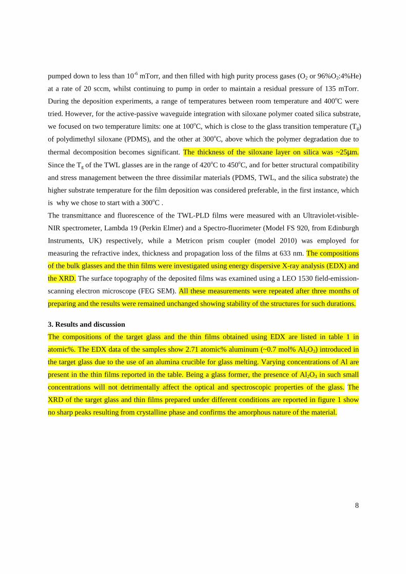
The compositions of the target glass and the thin films obtained using EDX are listed in table 1 in
atomic%. The EDX data of the samples show 2.71 atomic% aluminum (~0.7 mol% Al2O3) introduced in
the target glass due to the use of an alumina crucible for glass melting. Varying concentrations of Al are
present in the thin films reported in the table. Being a glass former, the presence of Al2O3 in such small
concentrations will not detrimentally affect the optical and spectroscopic properties of the glass. The
XRD of the target glass and thin films prepared under different conditions are reported in figure 1 show
no sharp peaks resulting from crystalline phase and confirms the amorphous nature of the material.
9
Table 1 The compositions of target and thin films in atomic% measured using EDX
Element/Glass thin filmsdeposited on
O Te W La Er Al
Silica substrate at 100oC in O2 87.3 6.0 3.4 1.4 0.2 1.7
Silica substrate at 300oC in O2 80.2 7.5 8.1 2.7 0.1 1.4
PDMS on silica substrate at100oC in O2
83.8 7.6 5.8 2.3 0.2 0.3
PDMS on silica substrate at100oC in 96vol%O2/4vol%He
81.6 7.7 6.2 2.4 0.2 1.9
Bulk glass 78.4 11.7 3.7 3.1 0.3 2.7
0 30 60 90
(d)
(c)
(b)
No
rmal
ized
inte
nsi
ty(a
.u.)
2θ
(a)
Figure 1. XRD of samples: (a) target glass, (b) glass film on silica deposited at 100oC, (c) glass film on
silica deposited at 300oC and (d) glass film on polymer deposited at 100oC
3.1 Optical properties and topography of thin films on silica substrates
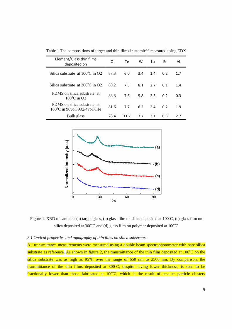
All transmittance measurements were measured using a double beam spectrophotometer with bare silica
substrate as reference. As shown in figure 2, the transmittance of the thin film deposited at 100oC on the
silica substrate was as high as 95%, over the range of 650 nm to 2500 nm. By comparison, the
transmittance of the thin films deposited at 300oC, despite having lower thickness, is seen to be
fractionally lower than those fabricated at 100oC, which is the result of smaller particle clusters
10
constituting the film at higher substrate temperature (see figure 3). The interference fringe patterns shown
in figure 2 are an indication of thickness uniformity of the films in the measured area.
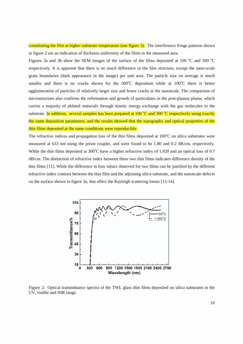
Figures 3a and 3b show the SEM images of the surface of the films deposited at 100 oC and 300 oC
respectively. It is apparent that there is no much difference in the film structure, except the nano-scale
grain boundaries (dark appearance in the image) per unit area. The particle size on average is much
smaller and there is no cracks shown for the 300oC deposition while at 100oC there is better
agglomeration of particles of relatively larger size and fewer cracks at the nanoscale. The comparison of
microstructure also confirms the reformation and growth of particulates in the post-plasma plume, which
carries a majority of ablated materials through kinetic energy exchange with the gas molecules to the
substrate. In addition, several samples has been prepared at 100 oC and 300 oC respectively using exactly
the same deposition parameters, and the results showed that the topography and optical properties of the
thin films deposited at the same conditions were reproducible.
The refractive indices and propagation loss of the thin films deposited at 100oC on silica substrates were
measured at 633 nm using the prism coupler, and were found to be 1.80 and 0.2 dB/cm, respectively.
While the thin films deposited at 300oC have a higher refractive index of 1.920 and an optical loss of 0.7
dB/cm. The distinction of refractive index between these two thin films indicates difference density of the
thin films [11]. While the difference in loss values observed for two films can be justified by the different
refractive index contrast between the thin film and the adjoining silica substrate, and the nanoscale defects
on the surface shown in figure 3a, that affect the Rayleigh scattering losses [12-14].
Figure 2: Optical transmittance spectra of the TWL glass thin films deposited on silica substrates in theUV, visible and NIR range.
11
Figure 3: SEM images of a TWL glass thin deposited over silica substrate at (a) 100 oC and (b) 300 oC
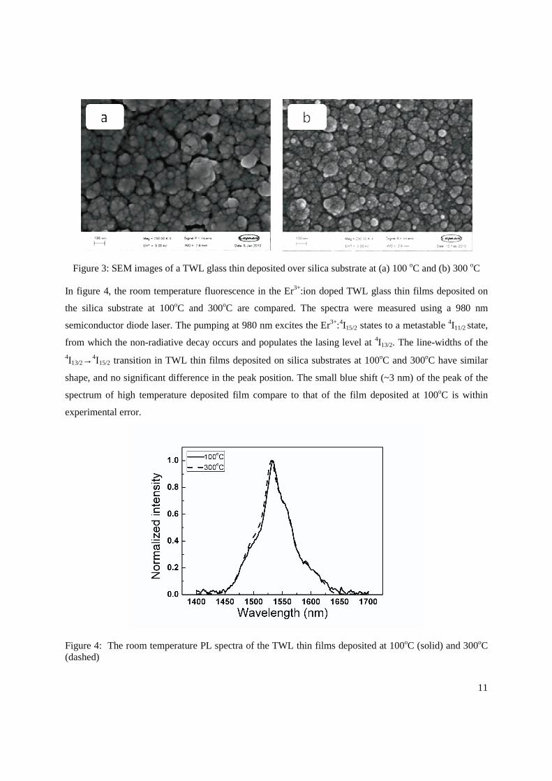
In figure 4, the room temperature fluorescence in the Er3+:ion doped TWL glass thin films deposited on
the silica substrate at 100oC and 300oC are compared. The spectra were measured using a 980 nm
semiconductor diode laser. The pumping at 980 nm excites the Er3+:4I15/2 states to a metastable 4I11/2 state,
from which the non-radiative decay occurs and populates the lasing level at 4I13/2. The line-widths of the4I13/2→4I15/2 transition in TWL thin films deposited on silica substrates at 100oC and 300oC have similar
shape, and no significant difference in the peak position. The small blue shift (~3 nm) of the peak of the
spectrum of high temperature deposited film compare to that of the film deposited at 100oC is within
experimental error.
Figure 4: The room temperature PL spectra of the TWL thin films deposited at 100oC (solid) and 300oC(dashed)
12
The values of the fluorescence bandwidth (∆λ= ∫Idλ/Imax) of two photoluminescence (PL) spectra are
reported in table 2, and the bandwidth of the films deposited at 100oC and 300oC are the same at 72 nm.
The lifetimes of the 4I13/2→4I15/2 transition are also compared as well as the experimental data of the
propagation losses, refractive index (at 633 nm) and thickness of the films are listed in table 2. And it can
be observed that the PL lifetime of the films deposited on silica is lower compared to that of the target.
This can be attributed to larger –OH concentration in the films resulting in increase of the nonradiative
relaxation from 4I13/2 level. The origin of these hydroxyl groups may be from the moisture present in the
process gas used during the deposition and the presence of nanoscale grain boundaries also favors
moisture adsorption.
Table 2: Optical and spectroscopic properties of TWL bulk glass and thin films deposited on plain and
polymer-coated silica substrates
Glass filmsdeposited on
Gasatmosphere
for deposition@ 135 mTorr
Refractiveindex at633 nm
(±0.0005)
Loss at633 nm(dB cm-1
±0.2)
Fluorescencebandwidth
(nm)
Lifetimes(ms)
4I13/2→4I15/2
(±0.02)
Thickness(µm)
(±(0.5% + 5nm))
Silicasubstrate at
100oCO2 1.8201 0.2 72 2.28 1.073
Silicasubstrate at
300oCO2 1.9213 0.7 72 2.00 0.983
PDMS onsilica substrate
at 100oCO2 1.6380 1.1 69 1.24 1.698
PDMS onsilica substrate
at 100oC
96 vol%O2-4vol% He
1.8954 0.1 71 1.22 0.784
Bulk glass - 2.0965 - 77 5.30 -
3.2 Optical properties and topography of thin films on PDMS coated on silica substrates
In our experiments we confined all the TWL glass on polymer-coated substrates deposition to
temperatures below 150oC to avoid polymer decomposition. Although these materials decompose readily
between 300 oC-400 oC [15], under high vacuum environments, such as the one in the PLD chamber, the
degradation of polymer structure can take place at even lower temperatures.
For the deposition of thin films on polymer-coated substrates, two different ambient gases were used in
the PLD chamber: high purity oxygen and a mixture of 96 vol % oxygen with 4 vol% of helium. The
13
reason for introducing helium (He) with O2 in the chamber at a comparable partial pressure is that the
ionization energy of He is higher than that of O2 (He: 24.59eV and O2: 13.62 eV), and the high energetic
He species (He radical and He ions) has the advantage of reducing the roughness of the thin film surface
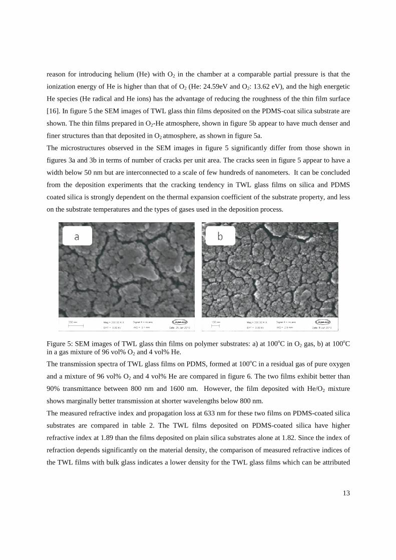
[16]. In figure 5 the SEM images of TWL glass thin films deposited on the PDMS-coat silica substrate are
shown. The thin films prepared in O2-He atmosphere, shown in figure 5b appear to have much denser and
finer structures than that deposited in O2 atmosphere, as shown in figure 5a.
The microstructures observed in the SEM images in figure 5 significantly differ from those shown in
figures 3a and 3b in terms of number of cracks per unit area. The cracks seen in figure 5 appear to have a
width below 50 nm but are interconnected to a scale of few hundreds of nanometers. It can be concluded
from the deposition experiments that the cracking tendency in TWL glass films on silica and PDMS
coated silica is strongly dependent on the thermal expansion coefficient of the substrate property, and less
on the substrate temperatures and the types of gases used in the deposition process.
Figure 5: SEM images of TWL glass thin films on polymer substrates: a) at 100oC in O2 gas, b) at 100oCin a gas mixture of 96 vol% O2 and 4 vol% He.
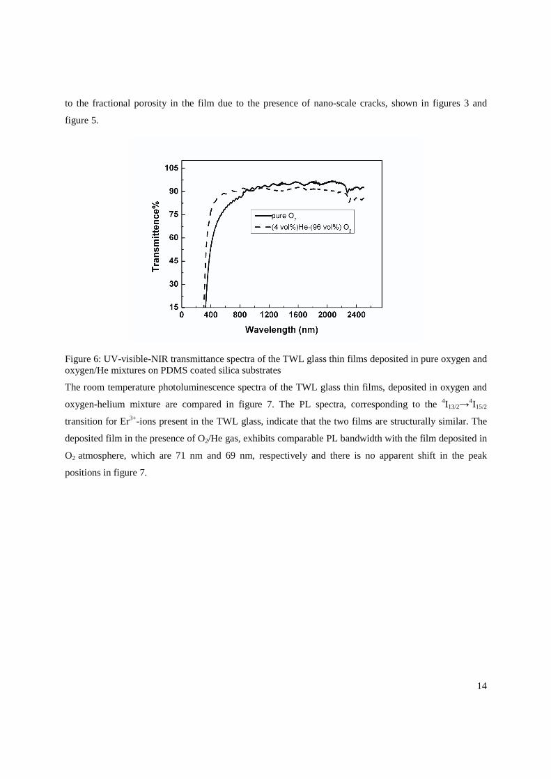
The transmission spectra of TWL glass films on PDMS, formed at 100oC in a residual gas of pure oxygen
and a mixture of 96 vol% O2 and 4 vol% He are compared in figure 6. The two films exhibit better than
90% transmittance between 800 nm and 1600 nm. However, the film deposited with He/O2 mixture
shows marginally better transmission at shorter wavelengths below 800 nm.
The measured refractive index and propagation loss at 633 nm for these two films on PDMS-coated silica
substrates are compared in table 2. The TWL films deposited on PDMS-coated silica have higher
refractive index at 1.89 than the films deposited on plain silica substrates alone at 1.82. Since the index of
refraction depends significantly on the material density, the comparison of measured refractive indices of
the TWL films with bulk glass indicates a lower density for the TWL glass films which can be attributed
14
to the fractional porosity in the film due to the presence of nano-scale cracks, shown in figures 3 and
figure 5.
Figure 6: UV-visible-NIR transmittance spectra of the TWL glass thin films deposited in pure oxygen andoxygen/He mixtures on PDMS coated silica substrates
The room temperature photoluminescence spectra of the TWL glass thin films, deposited in oxygen and
oxygen-helium mixture are compared in figure 7. The PL spectra, corresponding to the 4I13/2→4I15/2
transition for Er3+-ions present in the TWL glass, indicate that the two films are structurally similar. The
deposited film in the presence of O2/He gas, exhibits comparable PL bandwidth with the film deposited in
O2 atmosphere, which are 71 nm and 69 nm, respectively and there is no apparent shift in the peak
positions in figure 7.
15
Figure 7: Room temperature PL spectra of TWL glass films, deposited at 100oC on PDMS coated silicasubstrates in O2 and O2/He atmospheres.
As shown in table 2, the lifetime of films on polymer have a further reduction in the lifetime compare to
that of the thin film on silica, and this may be due to the formation of polymer-rare earth complexes at the
polymer-glass interface. To confirm the exact origin of the reduction of the transition lifetime observed
in the films deposited on two types of substrates, more detailed investigations are required.
Conclusions
High-quality TWL glass thin films were fabricated on plain and polymer-coated silica substrates using
PLD. The thin films of TWL glass formed at 100oC have a propagation loss of 0.21 dB/cm while the film
on polymer-coated substrate exhibited a lower loss of 0.1 dB/cm. We found from the refractive index
measurements that the higher temperature thin films were much denser than that deposited at 100oC. The
measured PL bandwidth and lifetimes of Er3+: 4I13/2 to 4I15/2 transition in the films are smaller than that in
the bulk glass. Further optimization of the deposition conditions is required to improve these
spectroscopic properties. The PLD method presented in this paper has potential for use for the fabrication
of glass -polymer integrated optical devices with both active and passive functionalities.
Acknowledgements
The authors acknowledge the financial support from the RCUK for their collaborative Basic Technology
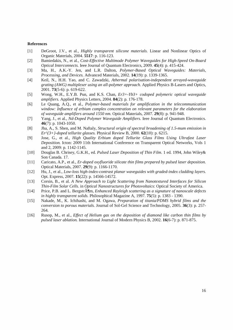
[1] DeGroot, J.V., et al., Highly transparent silicone materials. Linear and Nonlinear Optics ofOrganic Materials, 2004. 5517: p. 116-123.
[2] Bamiedakis, N., et al., Cost-Effective Multimode Polymer Waveguides for High-Speed On-BoardOptical Interconnects. Ieee Journal of Quantum Electronics, 2009. 45(4): p. 415-424.
[3] Ma, H., A.K.-Y. Jen, and L.R. Dalton, Polymer-Based Optical Waveguides: Materials,Processing, and Devices. Advanced Materials, 2002. 14(19): p. 1339-1365.
[4] Keil, N., H.H. Yao, and C. Zawadzki, Athermal polarisation-independent arrayed-waveguidegrating (AWG) multiplexer using an all-polymer approach. Applied Physics B-Lasers and Optics,2001. 73(5-6): p. 619-622.
[5] Wong, W.H., E.Y.B. Pun, and K.S. Chan, Er3+-Yb3+ codoped polymeric optical waveguideamplifiers. Applied Physics Letters, 2004. 84(2): p. 176-178.
[6] Le Quang, A.Q., et al., Polymer-based materials for amplification in the telecommunicationwindow: Influence of erbium complex concentration on relevant parameters for the elaborationof waveguide amplifiers around 1550 nm. Optical Materials, 2007. 29(8): p. 941-948.
[7] Yang, J., et al., Nd-Doped Polymer Waveguide Amplifiers. Ieee Journal of Quantum Electronics.46(7): p. 1043-1050.
[8] Jha, A., S. Shen, and M. Naftaly, Structural origin of spectral broadening of 1.5-mum emission inEr^{3+}-doped tellurite glasses. Physical Review B, 2000. 62(10): p. 6215.
[9] Jose, G., et al., High Quality Erbium doped Tellurite Glass Films Using Ultrafast LaserDeposition. Icton: 2009 11th International Conference on Transparent Optical Networks, Vols 1and 2, 2009: p. 1142-1145.
[10] Douglas B. Chrisey, G.K.H., ed. Pulsed Laser Deposition of Thin Film. 1 ed. 1994, John Wiley&Son Canada. 17.
[11] Caricato, A.P., et al., Er-doped oxyfluoride silicate thin films prepared by pulsed laser deposition.Optical Materials, 2007. 29(9): p. 1166-1170.
[12] Hu, J., et al., Low-loss high-index-contrast planar waveguides with graded-index cladding layers.Opt. Express, 2007. 15(22): p. 14566-14572.
[13] Corsin, B., et al. A New Approach to Light Scattering from Nanotextured Interfaces for SiliconThin-Film Solar Cells. in Optical Nanostructures for Photovoltaics: Optical Society of America.
[14] Price, P.B. and L. Bergström, Enhanced Rayleigh scattering as a signature of nanoscale defectsin highly transparent solids. Philosophical Magazine A, 1997. 75(5): p. 1383 - 1390.
[15] Nakade, M., K. Ichihashi, and M. Ogawa, Preparation of titania/PDMS hybrid films and theconversion to porous materials. Journal of Sol-Gel Science and Technology, 2005. 36(3): p. 257-264.
[16] Rusop, M., et al., Effect of Helium gas on the deposition of diamond like carbon thin films bypulsed laser ablation. International Journal of Modern Physics B, 2002. 16(6-7): p. 871-875.