Tenth International Symposium on Space Terahertz Technology, Charlottesville, March 1999 OPTIMIZATION OF THE NORMAL METAL HOT-ELECTRON MICROBOLOMETER D. Chouvaev, D. Golubev, M. Tarasov*, and L. Kuzmin Department of Microelectronics and Nanoscience. Chalmers University of Technology, SE-412 96 Gothenburg. Sweden *Inst of Radioengineering and Electronics RAS, Mokhovaya I 1 1 0390 7 Moscow. Russia Abstract The purpose of our project is to create a robust fully on-chip integrated antenna-coupled bolorneter, competitive in sensitivity for radio-astronomy applications. It must have noise 17 equivalent power (NEP) below 10 - W/Hz 112 and time constant shorter then 1 ms. We call this device a normal metal hot-electron microbolometer (NHEB), because its function is based on the hot-electron effect in a strip of a normal metal at temperatures below 0.5 K. Until now we have been developing the power sensor for this device. In the beginning we could not operate the sensor at electronic temperatures below 300 mK, presumably because of the high external noise load. Our latest results show how this problem can be solved experimentally. We have achieved noise performance mostly limited by the amplifier, which corresponds to expected detector NEP on the order of 1.5 . 10 -17 W/HZ I l2 at 100 mK. We have also performed a theoretical analysis of temperature readout by NIS tunnel junctions in our device. In particular heat flow fluctuations are discussed as an additional noise component, which needs to be included in the analysis. Our model allows us to calculate optimal ranges of parameters like normal resistance of the junction or optimal bias current, to provide the lowest NEP for given operating conditions (temperature, phonon noise etc.). 1. Introduction Bolometers are direct broad band detectors of electromagnetic radiation, complementing heterodyne detectors in radio-astronomy research. They are useful, for example, for investigating the cosmic microwave background. Most common bolometers used in radio-astronomy are made with a suspended absorber, being heated by incident radiation, and a semiconducting thermistor. Cooled to 100 mK, they can provide sensitivity better then 3 . 10 -17 W/Hz 1/2 with time constant down to 10 ms [1]. An alternative to those are superconducting bolometers, where the sensor is a suspended chip with a superconducting 552
Transcript
Tenth International Symposium on Space Terahertz Technology, Charlottesville, March 1999
OPTIMIZATION OF THE NORMAL METAL HOT-ELECTRONMICROBOLOMETER
D. Chouvaev, D. Golubev, M. Tarasov*, and L. Kuzmin
Department of Microelectronics and Nanoscience.Chalmers University of Technology, SE-412 96 Gothenburg. Sweden
*Inst of Radioengineering and Electronics RAS, Mokhovaya I 1 1 0390 7 Moscow. Russia
Abstract
The purpose of our project is to create a robust fully on-chip integrated antenna-coupledbolorneter, competitive in sensitivity for radio-astronomy applications. It must have noise
17equivalent power (NEP) below 10 - W/Hz 112 and time constant shorter then 1 ms. Wecall this device a normal metal hot-electron microbolometer (NHEB), because its functionis based on the hot-electron effect in a strip of a normal metal at temperatures below0.5 K.
Until now we have been developing the power sensor for this device. In the beginning wecould not operate the sensor at electronic temperatures below 300 mK, presumablybecause of the high external noise load. Our latest results show how this problem can besolved experimentally. We have achieved noise performance mostly limited by theamplifier, which corresponds to expected detector NEP on the order of 1.5 . 10-17 W/HZ
I l2
at 100 mK.
We have also performed a theoretical analysis of temperature readout by NIS tunneljunctions in our device. In particular heat flow fluctuations are discussed as an additionalnoise component, which needs to be included in the analysis. Our model allows us tocalculate optimal ranges of parameters like normal resistance of the junction or optimalbias current, to provide the lowest NEP for given operating conditions (temperature,phonon noise etc.).
1. Introduction
Bolometers are direct broad band detectors of electromagnetic radiation, complementingheterodyne detectors in radio-astronomy research. They are useful, for example, forinvestigating the cosmic microwave background. Most common bolometers used inradio-astronomy are made with a suspended absorber, being heated by incident radiation,and a semiconducting thermistor. Cooled to 100 mK, they can provide sensitivity betterthen 3 . 10-17 W/Hz 1/2 with time constant down to 10 ms [1]. An alternative to those aresuperconducting bolometers, where the sensor is a suspended chip with a superconducting
552
antenna or DC-bias
S
Tenth International Symposium on Space Terahertz Technology, Charlottesville, March 1999
structure. Being kept by electrothermal feedback at the superconducting transition, thissystem reacts strongly on signal-induced temperature variations around T,(3OO mK) [21
One disadvantage with the existing bolometers is that they compromise sensitivity andspeed — to reach NEP < 10 -17 W/HZ 112 one needs to make the absorbing area large, thusgetting also large thermal capacity and, consequently, longer reaction time. The thermalreaction time is defined as v----C/G, where C is the absorber' s thermal capacity and G isthermal conductance from the absorber to the environment.
Another problem is that suspended structures are often fragile, and it is difficult tocombine many of them into a 2D detector array. Building a fully planar-integrated 2Darray of detectors with sensitivity better then 10 -17 W/HZ 112 and time constant under 1 mscan be regarded as a challenge in bolometer research.
The device proposed in {3] and later partly implemented [4] can be a promising choice.This is a planar microfabricated bolometer, using an antenna (which can be integrated onthe same chip) to receive a signal. The schematic picture of the whole circuit and anSEM-image of a fabricated sensor can be seen in fig. 1. In an antenna-coupled bolometerthere is no need to make the sensor itself large to receive more power, instead it can beminiaturized, minimizing also the thermal capacity.
FIG. 1. The original device scheme and an SEM-image of a real sample. Double NIStunnel junctions are used to increase the response dV/dT and to simplify biasing.
A microwave signal received by the antenna will induce current in a normal-metal resistor(further referred to as "absorber"), this current will dissipate and generate Joule heat. Thisheat, however, will be delivered not to the whole structure at once, but first to the electrongas in the resistor. At temperatures below 0.5 K, where ultra-sensitive bolometers areoperated. the thermal coupling between electrons and phonons is very low, and theelectrons will establish their own equilibrium at a temperature above the phonontemperature in the surrounding body (hot electron effect). In this sense, the electron gas inthe resistor can be seen as a power absorber, and the thermal conductance to the
553
-500 0 500V. v,
-400 -200 200 400
T= 100 mKT = 300 mK
AG64-A, 2R N = 28 la211999-02-02)
1 . 01= 100 mKT = 300 mK
0.5
dV/dI = 53 M C2
= 350 k
-0.5
-1.0
AG77-A, 2R N = 30 k(1999-02-18)
30
20
10
-10
-20
-30
Tenth International Symposium on Space Terahertz Technology, Charlottesville, March 1999
environment is then limited by the energy exchange rate between the electrons and thephonons. Thus one does not need to suspend the absorber to thermally isolate it.Furthermore, the thermal capacity of the electrons is much less than the thermal capacityof the whole structure, and this makes the sensor very fast.
The only problem left is that the heated electrons could diffuse back to the antennainstead of exchanging energy with phonons in the resistor. Fortunately this can be avoidedby making the antenna superconducting, since a property of a superconductor-normalmetal interface is that electric current passes it without transferring the thermal energy ofelectrons (Andreev reflection).
Finally, very small signal power results in a substantial rise of the electron temperaturein the absorber. These temperature variations need to be converted to some electricalresponse, and this is accomplished using one or two normal-metal/insulator/superconductor (NIS) tunnel junctions, where the normal electrode is the absorber.Their IV-characteristics get broadened with increasing electron temperature in the N-electrode. When such a junction (or a pair of those) is biased with constant current inthe sub-gap region, the voltage over the junction will depend on the thermal smearing.and it will be proportional to the electron temperature in a wide range (fig. 2).
FIG. 2. Principle of measuring electron temperature by means of an NIS or SINIS tunneljunction stucture biased with constant current.
The power responsivity of this sensor is a ratio of two terms: temperature responsivity(d V/d7) and heat conductance from the electrons to the environment (G = dP/c17):
dV dV dP
dP dT dT
-1000
554
Tenth International Symposium on Space Terahertz Technology, Charlottesville, March 1999
The temperature responsivity depends on properties of the tunnel junctions and it isnearly constant almost in the whole range of operating temperatures (typicallyd 5-10•104 V/K). The heat conductance depends mostly on properties of theabsorber and can be estimated from the ideal energy exchange rate between electronsand phonons in equilibrium at different temperatures:
P =EQ,(Te5 — )
dP= 5/K2Te4
dT
where Q here is the absorber volume and I is a specific material parameter. For realisticdevice parameters (namely for our sample AG77) this gives power responsivity
Accordingly, a decrease of the operating temperature has great advantages, limited thoughby the fact that dV/dT rapidly falls below 100 mK. Knowing the power responsivity, wecan also estimate the noise equivalent power (NEP) of the detector. Assuming that thetotal noise is dominated by amplifier noise, and that we use a very good amplifier(\
i'Sv = 3nV/Hz 1/2) we get
NEP(0.3K) = 3.10-17 4/ ' NEP(0.1K) =1 . 10-18 -
which is superior to most of the existing devices.
The thermal reaction time will be determined by the electron-phonon interaction time.estimated to
r 2 . 10 -8 T,-3 sK 3 1(0.3K) = 0.8,us , z (0.1K) = 201us
This is also well below of what is usually required (1 ms).
2. Device fabrication and measurement setup
The power sensor ("microcalorimeter") is fabricated by e-beam lithography and shadowmetal evaporation. Three metal layers are used — a superconductor for NIS tunnel junc-tions (aluminum film, 36-38 nm), a normal metal for the power absorber (copper, 58 nm),and one more superconducting layer for the absorber bias leads or eventually the antenna(aluminum, 70 nm). The tunnel junctions are formed by oxidizing the firstsuperconducting layer before deposition of the normal metal on top of it Typicaloxidation conditions are P(0 2) = 0.3-0.4 mbar and t = 0.5-2 min, this results in thejunction normal resistance of 5-15 IcS2 for area about 0.1 pt,m2 . The tricky part is to contactthe same absorber strip both by an oxidized superconductor (NIS junctions) and by asuperconductor with a very transparent interface to the normal metal (absorber biaselectrodes). This can be done either by a two-step process with two
555
:.AI-AiOx.
Tenth International Symposium on Space Terahertz Technology, Charlottesville, March 1999
lithography/deposition steps and ion beam cleaning in-between, or by our new single-stepprocess where tilting of a sample in two perpendicular planes is employed (fig. 3).
The dimensions of the absorber in the most recent modification of our device are4.5x0.25 gm 2, thickness 58 nm, copper. Its resistance is about 20 S2, which is not optimalfor matching to an antenna. That is why we are planning to decrease the width to 0.1 gmand increase the length in the future. Changing the absorber material to chromium isanother option.
For dc-measurements we have used a current bias to introduce heat into the absorberinstead of connecting any antenna. The measurements are done in a dilution refrigeratorcapable of cooling samples to 25 mK. There is no possibility to irradiate a sample withsub-mm-waves in this cryostat. The current source for the NIS junctions' bias (and thesame kind for the absorber bias) is made up of a symmetric voltage source and two high-value (10 or 100 MO) resistors in series (at room temperature). Johnson noise in thoseresistors is the main source of bias noise discussed in part 4.
FIG. 3. Schematic picture of the metal deposition process. A double PMMA-copolymerresist is used to make a suspended mask. In the leftmost picture both resist layers areshown by slightly darker areas, on the three others — only the underlying copolymer mask.By tilting the sample in different planes the metal structures are shifted in respect to theoriginal openings in the PMMA-mask, providing also necessary overlaps betweensubsequently deposited metal layers.
Tenth International Symposium on Space Terahertz Technology, Charlottesville, March 1999
The measurements include a calibration measurement, where the voltage response fromthe tunnel junctions at the working bias is studied as a function of temperature in thecryostat without applying any additional heating to the absorber. IV-curves of the tunneljunctions at different cryostat temperatures are registered to determine or verify the choiceof the working point, as well as for diagnostics of the junction quality. Then we can testthe sensor by driving current through the absorber and measuring the response at a fixedcryostat temperature. Finally, noise spectra at different measurement conditions can betaken.
3. Experimental results
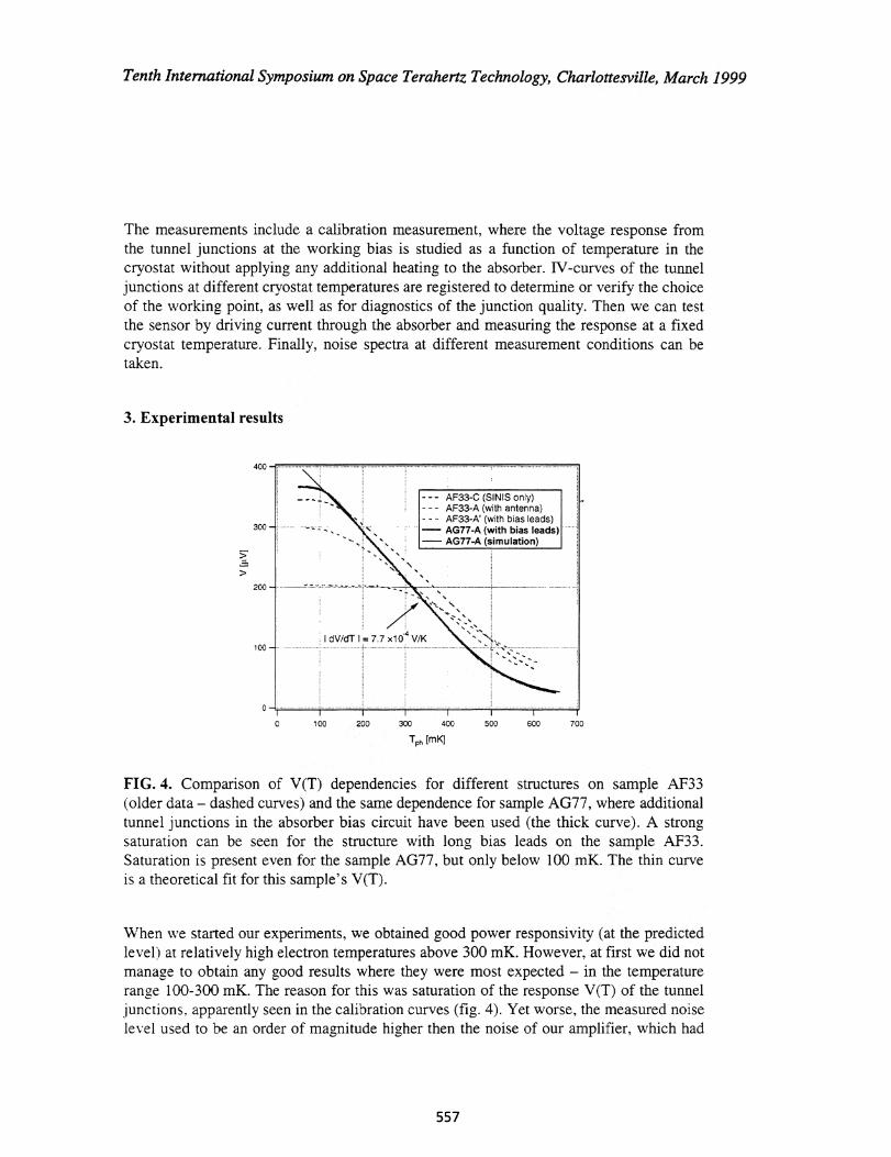
FIG. 4. Comparison of V(T) dependencies for different structures on sample AF33(older data — dashed curves) and the same dependence for sample AG77, where additionaltunnel junctions in the absorber bias circuit have been used (the thick curve). A strongsaturation can be seen for the structure with long bias leads on the sample AF33.Saturation is present even for the sample AG77, but only below 100 mK. The thin curveis a theoretical fit for this sample's V(T).
When we started our experiments, we obtained good power responsivity (at the predictedlevel) at relatively high electron temperatures above 300 mK. However, at first we did notmanage to obtain any good results where they were most expected — in the temperaturerange 100-300 mK. The reason for this was saturation of the response V(T) of the tunneljunctions, apparently seen in the calibration curves (fig. 4). Yet worse, the measured noiselevel used to be an order of magnitude higher then the noise of our amplifier, which had
557
-4 -2 0SINIS bias current, nA
2 4 "f„.. er re{
• Voltage noise (band 20-45 Hz)- Temperature responsrvity ANTAT
Tenth International Symposium on Space Terahertz Technology, Charlottesville, March 1999
modest 30 nV/Hz 1/2 at 10 Hz. It has taken a while to realize that those phenomena musthave had the same cause, namely an intensive and noisy input signal, coupling to theabsorber and heating the electrons sometimes above +300 mK. Two clues convinced usof the validity of this hypothesis: a comparison of noise and gain (=power responsivity) ofthe device (fig. 5a) and the dependence Telectrong p.onon, of) Of the absorber where Telectron hadbeen deduced by fitting IV-curves of the tunnel junctions at different temperatures(fig. 5b).
a) b)
FIG. 5. a) Spot noise and dV/dT plotted on the same graph for one of the older samples:both dependencies have very similar shapes, which must indicate that the noise is presentalready as fluctuations of electron temperature in the absorber, i.e. at the input. b) Telectron
(deduced from fits of IV-curves for SINIS double junctions) vs. temperature Tp h at whichthose IV-curves have been taken; data for sample AF33 (see also fig. 4).
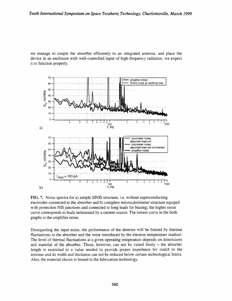
Once being convinced about the presence of external heating we tried to identify how thenoise comes in. Pick-up in the circuit connected for heating the absorber was onesuggestion, a microwave "leakage" into the sample cavity was another one. Eliminatingthe second being a more difficult task, we started by breaking the absorber bias circuit byhigh-resistive elements close to the absorber. We hoped that the voltage induced in thatlow-ohmic (Rabs = 20 K2) circuit by microphonics will drop on those high-resistive links,thus not being able to generate any noticeable current. We have chosen NIS tunneljunctions on both sides of the absorber as such protecting links, since they have very highintrinsic resistance in the sub-gap region, and they are very easy to fabricate (fig. 6).
This measure has given surprisingly good results, bringing the V(T) saturation down to100-130 mK (fig. 4), and the noise level almost to the amplifier level. However, if welook at the noise spectra (fig. 7), we may notice, that connecting wires to the absorber andclosing this circuit result in additional noise contributions, thus indicating that even thisstrong protection is not perfect. Furthermore, even the noise associated with an isolated
558
Tenth International Symposium on Space Terahertz Technology, Charlottesville, March 1999
"absorber" island (7-10 nV/Hz 1 /2 ) is clearly higher then what is expected from the
thermometry noise (3 nV/Hz 1/2). We think that some high-frequency leak still exists andthat it is responsible for this additional noise. Re-calculated to NEP the measured voltagenoise corresponds to about 1.5-10 -17 W/Hz 1/2 at 10 Hz.
antenna or DC-bias
Es■—•
N-I-S S-I-N
S-I-N N-I-S
FIG. 6. The modified structure with additional NIS tunnel junctions in the absorber biascircuit.
However, the protection by tunnel junctions distorted completely the heating powercalibration at 'absorber > 0. Earlier we could assume that the dissipated power wasP=PJ=RabsorberXfabsorber• Now, as soon as Ibias>0 high-energy electrons are injected into thesuperconducting electrode of the protecting NIS-junction, and further to the absorber,where this energy apparently dissipates, giving P>>Pj. This effect is similar to theelectronic cooling by NIS tunnel junctions described elsewhere [5], but now our object ison the "warm" side of the Peltier cooler. This is the reason why we still can not report thecalibrated experimental value of the power responsivity of our device at low temperature(100 ml().
This unfortunate situation does not seem to be a real obstacle. Simply reversing the NISjunctions and thus setting the N-part at the absorber side should be enough to solve theproblem. An additional NS-interface between the superconducting electrodes going to theabsorber and the N-side of the protecting junctions would interrupt the unwanted energyflow due to the Andreev reflection. Another simple (but probably not as elegant) solutionis to use small external resistors, which can be bonded to the chip wiring, instead oftunnel junctions as high-resistive links.
Whatever difficulties can be expected in characterizing the device by applying a dc-current. the new results show that there are no severe problems with the sensor itself. If
559
- amplifier noise- SINIS noise at working bias
- bolometer noise,absorber bias i=0
- bolometer noise,absorber bias not connected
- amplifier noise
Tenth International Symposium on Space Terahertz Technology, Charlottesville, March 1999
we manage to couple the absorber efficiently to an integrated antenna. and place thedevice in an enclosure with well-controlled input of high-frequency radiation. we expectit to function properly.
70
60
50
40
30
20
10
0
a)
70
60
50
u- 40
30
20
10
0
b)
f, Hz
FIG. 7. Noise spectra for a) simple SINIS structure, i.e. without superconductingelectrodes connected to the absorber and b) complete microcalorimeter structure equipedwith protection NIS junctions and connected to long leads for biasing; the higher noisecurve corresponds to leads terminated by a current source. The lowest curve in the bothgraphs is the amplifier noise.
Disregarding the input noise, the performance of the detector will be limited by thermalfluctuations in the absorber and the noise introduced by the electron temperature readout.The level of thermal fluctuations at a given operating temperature depends on dimensionsand material of the absorber. Those, however, can not be varied freely — the absorberlength is restricted to a value needed to provide proper impedance for match to theantenna and its width and thickness can not be reduced below certain technological limits.Also, the material choice is bound to the fabrication technology.
560
Photon noisefrom apparatus
Photon noisein the signal
Noise in the biasAmplifier noise
Fluctuations in- the heat flow thru
a tunnel junction
READ-OUTThermal
fluctuations
Tenth International Symposium on Space Terahertz Technology, Charlottesville, March 1999
On the other hand. the noise from the read-out is a function of many parameters (tunneljunction resistance, number of the junctions, working point, amplifier performance etc.),which can be readily adjusted. Moreover, the noise contribution from the read-out willdominate in all practical configurations. That gives a motivation for optimizing the read-out parameters, and in the following section we will discuss what calculations can aid thisprocess.
4. Optimizing the readout performance
FIG. 8. Scheme of different noise contributions in the NHEB.
Different noise contributions adding to the useful input signal are depicted in fig. 8. Thenoise equivalent power of the detector can be expressed as
2
S Idl
hias (0) —dr/
+2e1
dV
+ Srvi (0) + S it/2'1'P (0)
dI ,VEP 2 NE.13
12,, + 41 cB T 2 ( G — G 7.1 ) ÷ S p (0) + G2
IdV/c/T121
where
ATP is the photon and other noise coming with the signal to the input,
561
, 1 8(E2 — 6,2 (Ts))e PO , , Ts )= f de
e 2 R N Ve2 — 6,2(rs) (6° — V Xf,, — e — f (e)]
Tenth International Symposium on Space Terahertz Technology, Charlottesville, March 1999
41c,T 2 (G — arj ) — noise from thermal fluctuations in the absorber. (G-G-n) is the thermal
conductance from the electron gas in the absorber to the lattice and environment.The thermal conductance due to the tunnel junctions is excluded here. since it isincorporated in the next term,
S p (0) — "heat flow noise", a component similar to shot noise. but related to the transferof energy by quasi-particles tunneling through the junction.
2e1coth(e 2e1 — current fluctuations due to discreteness of charge (shot noise)
s lbws (0) current fluctuations in the external bias applied to the junction
SrymPl (0) -- voltage noise of the amplifier (we assume a high-impedance FET-amplifier)
s fi tck-up \) voltage induced in the leads going from the sample to the amplifier
(microphonics and rf-field detection)
dV — temperature responsivity of an NIS-junction at the working bias. and
G — total thermal conductance from the electron gas in the absorber to its environment.
One term here is "new" in the sense that it, to our knowledge, has not been included inany similar analysis before, and this is S p (0) [6]. If a voltage less then die is applied overan NIS junction, there will be an energy flow from the normal metal to thesuperconductor. The effect can be used to cool the normal metal [5] and, accordingly, thisenergy flow is often called "cooling power":
where TAT and Ts are temperatures of the normal and superconducting electrodes, zi('rs) isthe gap in the superconductor, and fs are electron distributions in respective electrodes.This expression is very similar to the expression is very for current goin g through an NISjunction
de7 19(E 2 46,2 (Ts ))E rLIN (e— eV )— fs (e)]eR, A 2 fp \LA
S
but here every tunneling event results in transferring a portion of energy (e-eV). Since thetunneling events are random and independent, there will be a heat flow noise similar tothe usual shot noise. Calculating its spectral density is, however, somewhat morecomplicated, since the portions of energy are not all the same. The way to do this is to
562
Tenth International Symposium on Space Terahertz Technology, Charlottesville, March 1999
integrate contributions dS p = 2(e — eV)coth(eV 12T)PecIE from electrons with a par-
ticular energy in the range (e, e+de) over all possible energies:
V +S
2p (0)= coth
ed
e 2 RN 2T6 e 62 AEI — eVYVN — e V (e)]
/e 2 6,2 (Ts )
The heat flow noise is growing with applied voltage, respectively applied current, thusaffecting the upper limit of the optimal range of the bias current for the temperaturereading.
From the expression for the total noise one can see that the individual contributions fromthe different noise sources depend on the absorber properties (G), the shape of the NISjunction's IV-curve (dV/d1, dV/d7), and the working point /=/bias. It is also worth to noticethat in the theoretical calculations the temperature responsivity dV/ dr as a function ofbias current I can have a logarithmic singularity at 1-40 (be arbitrary large). This may bemisleading (suggesting very low bias currents), because this singularity does not exist innature, being destroyed by fluctuations near 1=0.
We can use a computer program to simulate the total noise for any given set ofparameters. For the integral giving the P1-characteristics of an NIS junction there is agood analytical approximation, which is suitable for fast calculations. But this is not thecase for the heat flow integral, and its computing in every point slows down the model alot. Fortunately we can separate the tasks. Sets of noise data can be pre-compiled for aspecific working temperature T, superconductor with energy gap A, and tunnel junctionquality in terms of sub-gap conductance r0 =R(0)/RN. Then we can combine those half-ready arrays by substituting all the other parameters of the device:
absorber size and material IQ,current bias source with noise Sl.bias(0),amplifier with noise Sampl(0),input noise NEP m r, ,normal resistance of tunnel junctions RAT, andworking bias current 'bias
This can be done really fast, and we have actually made a computer program where onecan gradually tune any of those parameters and see on a screen in real time how it affectsevery noise component and the total NEP. Examples of how the different noisecomponents and the total NEP depend on the SINIS bias current are given in fig. 9 fortwo different values of RN and two different temperatures.
563
• • ■••,
100101 i02
I pA
101'
b)162
pa .0`C` -03a)
_Thermal fluct
1 6"
10 18
10' .
\T-Total NEP0A.
-18[ N,10
o.„030.
&TVA,Tval NE.
- 00=00,,
161''NEP,WirtHz
amplifierShot noise
10NEP,W/ttHz
IThermal fluct.
162'I
10•2'Heat flow Putt.\ Heat flow fluct
162 1
4+
1622 10-n
--
1
1
••
2103101c) 102pa
1Cp0
10104 102 -02d)
Tenth International Symposium on Space Terahertz Technology, Charlottesville, March 1999
1
10•
NEP,W/rt Hz
Shot noise 0
Total NEP
'00- .....10
NEP.WIHz •
amp Per
""y_a!
_
'
Shci r.ceeThermal ftact.
-`,0000000,' ThermalHeal uct
10Heat flow Pact.
•
• • •
FIG. 9. Different noise components and the total noise calculated as function of SNISbias current for R1v=1 kf2 (a,c) and RN = 30 1d2 (b,d) /RN per one junction/ assumingworking temperature of T=300 mK (a,b) and T=100 mK (c,d).
5. Conclusion
We have managed to demonstrate a reasonable performance of the microcalorimeterwhich we aim to use as power sensor in an integrated antenna-coupled bolometer. Wecould do this also at temperatures below 100 mK, where the responsivity of the sensor ismuch higher than in our earlier results (for 300 mK). The measured noise levelcorresponds to about NEP = 5 . 10-18 W/Hz I/2, and it is dominated by the input noiseexternal to the sensor itself and the amplifier noise. Some refinement of the experiment isstill needed to make a fully calibrated characterization of the device.
We considered the noise components determining the practical performance of the futuredetector, some of them not referred to in earlier analyses of the similar kind. In particular,we payed attention to the heat flow noise, important at higher thermometer bias currents.We also showed how noise optimization can be performed in a model, co-adjusting twoor several device and operation parameters at the same time.
564
Tenth International Symposium on Space Terahertz Technology, Charlottesville, March 1999
References
[1] P.L. Richards, J. Appl. Phys. 76 (1), 1 (1994).
[2] A.T. Lee, S-F. Lee, J.M. Gildemeister, and P.L. Richards, Proc. of the 7th Int.workshop on Low Temperature Detectors, Munich, July-Aug 1997, pp 123-125.
[3] M. Nahum, P.L. Richards, and C.A. Mears, IEEE Trans. Appl. Supercond. 3, 2124(1993).
[4] M. Nahum and J. Martinis, Appl. Phys. Lett. 63(22), 3075 (1993).