N. Blanc, P. Giffard, P. Seitz, P. Buchschacher, V. Nguyen, and M. Hoheisel
Abstract Silicon is an excellent detector material for electromagnetic radiation in the wavelength range of 0.1–1,000 nm. In the visible spectral range (400–700 nm), external quantum efficiencies approaching 100% are obtained. When combined with the amazing miniaturization capabilities of the semiconductor industry, this fact explains why silicon is the material of choice for very efficient, highly integrated, cost-effective image sensors: In 2007 about one billion image sensors were produced and employed in camera systems. Profiting from the unrelenting progress of semiconductor technology, silicon-based image sensors with astounding performance have been demonstrated, in terms of resolution, pixel size, data rate, sensitivity, time resolution, and functionality: 111 million pixels on a single CCD chip were produced; pixels with a period of 1.2 mm were fabricated; sustainable image acquisition and readout rates of four billion pixels per second were realized; single-photon sensitivity at room temperature and at video rates was achieved; timing resolution of the pixels in lock-in image sensors below 5 ps was obtained, and the processing complexity of “smart pixels” was raised to several ten thousand transistor functions per pixel. The future of semiconductor image sensing lies in the extension of the accessible wavelength range to the infrared spectrum (1.5–10 mm), the development of affordable, high-performance X-ray image sensors, in particular, for the medical energy range (20–120 keV), the realization of sensitive and cost-effective sensors for Terahertz imaging (100–500 mm), as well as the integration of an increasing amount of analog and digital functionality on single-chip custom camera systems. The Holy Grail is the “seeing chip,” capable of analyzing the contents of a scene and of recognizing individual objects of interest.
Over the last decade, electronic imaging has made tremendous progresses, basically replacing film-based cameras in almost all application fields, including consumer, security, industrial, and scientific applications. These cameras rely on the excellent optoelectronic properties of semiconductor materials, with silicon being in most cases the material of choice. High quantum efficiency over the visible range and the cost-effective manufacturing capability of the semiconductor industry have enabled the production of image sensors at affordable prices with excellent performances, in particular in terms of spatial resolution, pixel size, dynamic range, and sensitivity. Until the year 2000 the large majority of commercially available electronic cameras and camcorders were based on charge coupled devices (CCDs). Today CCDs still play an important role in electronic imaging, due to their high performances providing for example spatial resolution of up to 111M pixels, dynamic range in excess of 80dB and sensitivity down to single-photon detection. However, complementary metal-oxide-semiconductor (CMOS) image sensors have been since the 1990s the subject of significant development. They take advantage of the capability to integrate analog and digital circuits on chip for the control and readout electronics. This on one hand enables the manufacture of cost-effective image sensors and on the other hand allows the realization of imagers with added functionalities, leading to increasingly smarter and more compact imaging devices. As a result, CMOS image sensors have today become worldwide the dominating technology both in terms of units sold as well as in terms of revenues. CMOS image sensors are now widely used for consumer applications, such as in compact digital still picture cameras (DSCs), mobile phones and camcorders, as well as in numerous other fields, including surveillance, security, robotics, automotive, industrial control and even medical applications.
CMOS image sensors clearly profit from the progresses realized in the semi-conductor industry and the continuous trend toward miniaturization, smaller minimal feature size, and the increased numbers of transistors/pixels per unit area, following in this regard Moore’s law as often referred to for other integrated circuits such as processors and memories. On the other hand the trend in the development of image sensors goes beyond just a race for more pixels and a higher level of integration. Image sensors are more and more used for applications covering a significant broader spectral range, from X-ray up to Terahertz imaging. Moreover, the development of smart imagers opens up completely new possibilities, for example, in three-dimensional imaging, object tracking, smart intrusion detection, or spectral imaging.
The present chapter gives an overview on the fundamentals of semiconductor image sensing and technology, giving insights in current technological trends and the state of the art in high-sensitivity electronic imaging. This is followed by application examples in high-speed imaging, color imaging, and optical 3D time-of-flight imaging. While many applications and products are focused on the visible range of the electromagnetic spectrum, the extension toward shorter wavelength (e.g., X-ray imaging) and longer wavelength (such as infrared and Terahertz imaging) is gaining in importance. Examples of IR sensors include quantum well IR photodetectors,
8 Semiconductor Image Sensing 241
BookID 152004_ChapID 8_Proof# 1 - <Date>
bolometers, and HgCdTe sensors. Magnetic resonance and ultrasound imaging in turn are not addressed within the scope of this chapter.
8.2 Fundamentals of Semiconductor Image Sensing
8.2.1 Interaction of Light and Semiconductor
The capability of solid-state image sensors to detect light is related to their semiconducting properties. The interaction of light and semiconductors has two principal components. First, light waves travel at a reduced speed c
mat = c
vac/n,
where n is the refractive index of the material and cvac
= 3 × 10⁸ m/s is the speed of light in vacuum. Second, the incident light intensity I
0 (W/m2) is absorbed
exponentially with the thickness x of the material through which it traveled, according to Beer’s law:
ff ,eL n
kl =
(8.1)
The absorption coefficient a (in units of cm−1) depends strongly on the wavelength and thus the energy of the incident light: For energies below the bandgap E
g, the
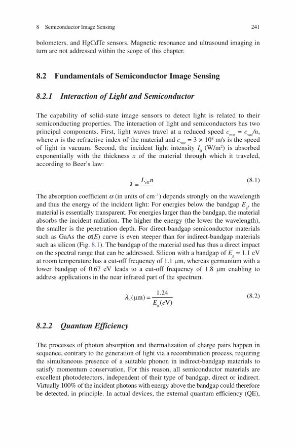
material is essentially transparent. For energies larger than the bandgap, the material absorbs the incident radiation. The higher the energy (the lower the wavelength), the smaller is the penetration depth. For direct-bandgap semiconductor materials such as GaAs the a(E) curve is even steeper than for indirect-bandgap materials such as silicon (Fig. 8.1). The bandgap of the material used has thus a direct impact on the spectral range that can be addressed. Silicon with a bandgap of E
g = 1.1 eV
at room temperature has a cut-off frequency of 1.1 mm, whereas germanium with a lower bandgap of 0.67 eV leads to a cut-off frequency of 1.8 mm enabling to address applications in the near infrared part of the spectrum.
cg
1.2
(m .
V)
4( )
E el m =
(8.2)
8.2.2 Quantum Efficiency
The processes of photon absorption and thermalization of charge pairs happen in sequence, contrary to the generation of light via a recombination process, requiring the simultaneous presence of a suitable phonon in indirect-bandgap materials to satisfy momentum conservation. For this reason, all semiconductor materials are excellent photodetectors, independent of their type of bandgap, direct or indirect. Virtually 100% of the incident photons with energy above the bandgap could therefore be detected, in principle. In actual devices, the external quantum efficiency (QE),
defined as h = number of photogenerated charge pairs/number of incident photons, is smaller than 100% for the following reasons:
1. Fresnel reflection of the incident light at the surface of the device.2. Multiple reflections in thin layers covering the device. This causes the characteristic
thin film interference oscillations in the spectrum.3. Absorption of the incident light either in the covering layers or in the electrically
inactive part of the semiconductor near the surface.4. Absorption deep in the semiconductor, at a distance greater than the diffusion
length L, where charge carrier pairs recombine instead of being able to diffuse to the depletion region of the photodetector near the surface.
5. The semiconductor is too thin (too transparent) so that not all the incident light is absorbed and parts of it (the longer wavelengths) are transmitted.
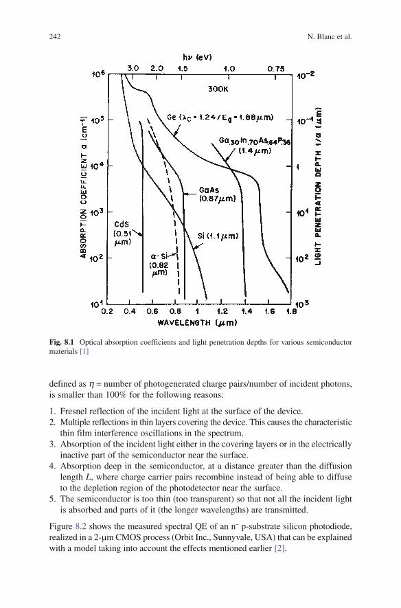
Figure 8.2 shows the measured spectral QE of an n− p-substrate silicon photodiode, realized in a 2-mm CMOS process (Orbit Inc., Sunnyvale, USA) that can be explained with a model taking into account the effects mentioned earlier [2].
Fig. 8.1 Optical absorption coefficients and light penetration depths for various semiconductor materials [1]
8 Semiconductor Image Sensing 243
BookID 152004_ChapID 8_Proof# 1 - <Date>
The QE h is a measure of the number of photogenerated electronic charges per incident photon. If, instead, the generated photocurrent I
ph (A) is measured as a
function of the incident light power P (W) at the wavelength l, the corresponding responsivity R (in units of A/W) can be defined as
ph .I
RP
= (8.3)
R is obviously related to the quantum efficiencyh:
( ) ( ),q
Rhc
ll h l= (8.4)
with Planck’s constant h = 6.63 × 10⁻³⁴ J s, and the speed of light in vacuum c = 3 × 10⁸ m/s.
8.2.3 Temperature Effects: Dark Current
The strongest impact of temperature is undoubtedly related to leakage currents. The so-called dark current (i.e., current measured without any applied optical signal) significantly varies from one technology to another with CCD still providing the best figures (below 1 pA/cm2). Optimized CMOS processes for image sensing
Fig. 8.2 Comparison of a model of the quantum efficiency (dashed line) and actual measure-ments (solid line) of a photodiode, realized with a standard 2.0-mm CMOS process [2]
technologies report figures of a few 10 s of pA (30–50 pA/cm2) at room temperature. It is important to note that the dark current depends strongly on temperature, rendering high-temperature applications very challenging. This dependence is essentially given by that of the intrinsic carrier concentration n
i in the semiconductor:
g3
22i e .
E
kTn Tµ- (8.5)
With Eg = 1.11 eV for silicon at room temperature the dark current is found to
double roughly every 10°C. Experimentally this doubling occurs even every 7–8°C. Thus, cooling the sensor by 25°C leads to a decrease of the dark current by almost a decade, which is significant and explains why most scientific cameras targeting applications with long exposure time (e.g., in astronomy) still need to be cooled. The current trend toward higher integration and smaller design features leads to typically higher doping levels and increased leakage current and dark current densities. This renders the realization of imagers providing high performances especially under low-light conditions even more challenging. In this specific case the higher integration/continuous trend toward miniaturization basically works against key performance figures of imaging devices.
8.2.4 Photosensor Principles: Photodiode and CCD
In image sensors the photogeneration of an electrical signal takes place in most cases either in a photodiode (i.e., a p–n junction) or in a MOS capacitance. Other approaches involve the use of specialized devices such as avalanche photodiodes (APDs) and phototransistors. Generally speaking photodiodes are used in CMOS image sensors, whereas MOS capacitances are preferably implemented in CCD imagers. However, interline transfer CCDs as mostly used in consumer cameras are typically based on photodiodes as photosensitive elements, whereas some CMOS imagers take advantage of photogates, a structure that is basically derived from CCD imagers.
Assuming a pixel size of 10 × 10 mm2, a fill-factor of 100%, and a quantum efficiency of 100%, an illumination level of 1 lux (which corresponds to about 1016 photons/s m2 for white light) leads to a photocurrent of the order of 160 fA. To effectively read out such low signals special care must be taken. Different detection circuits have been developed over the last decades to address this challenge, the simplest and also most often implemented one being a source follower. In this approach the photogenerated current is first integrated during a given integration time T
int onto a capacitor C. After this integration/exposure time, the charge DQ
accumulated is converted to an output voltage DVout
according to
int
photoo
( )d ,T
Q i t tD = ò (8.6)
8 Semiconductor Image Sensing 245
BookID 152004_ChapID 8_Proof# 1 - <Date>
out a( / ) ,V Q C gD D= (8.7)
with a 0.6 0.8 1g » - » being the “gain” of the source follower.For a capacitance of C = 10fF, the conversion gain amounts to q/C =16mV/e
leading to a measurable signal for typical charge packet of a few thousands of electrons. Higher conversion gain can be achieved by lowering the capacitance, or using current amplifier with very small feedback capacitances. This becomes mandatory if one wants to detect small signals, ultimately reaching for single electron and photon detection.
8.3 Semiconductor Technology for Imaging
8.3.1 Silicon Sensors
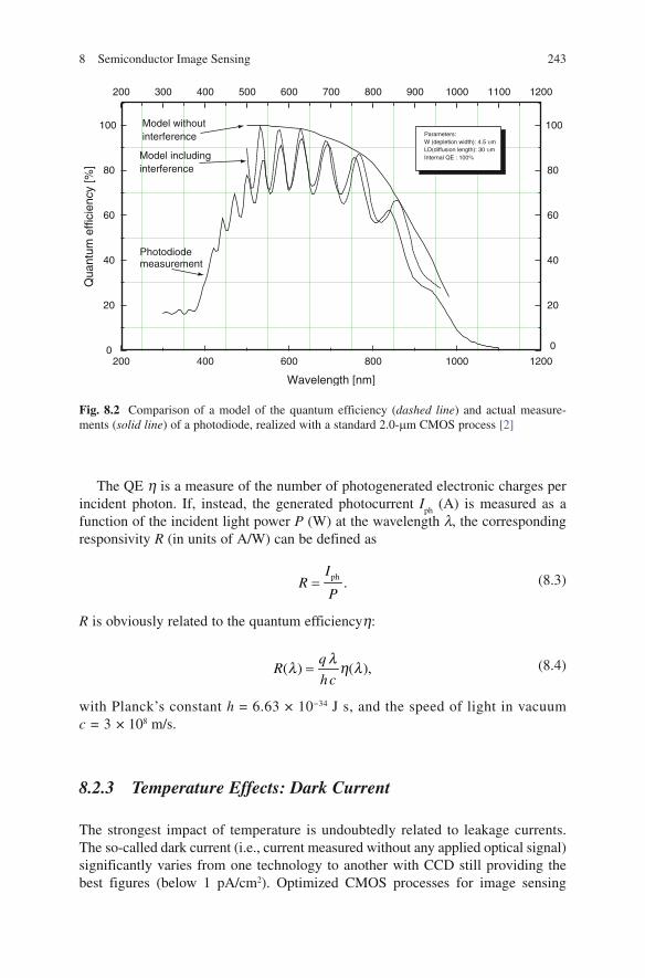
The unrelenting progress of semiconductor technology made it possible in the early 1960s to fabricate reliably several ten thousand transistors on the same chip. This capability was quickly used for the production of semiconductor image sensors using the then-available MOS process technology. These image sensors were based on the photodiode pixel architecture illustrated in Fig. 8.3. Each pixel consists of a photodiode that can be connected individually to an output amplifier through a row-select transistor connecting the photodiode to a column electrode, and through a column-select transistor connecting the column to the video output line.
Fig. 8.3 Architecture of photodiode-based image sensors: (a) MOS or photodiode array, (b) CMOS-compatible active pixel sensor (APS) imager
The charge detector measures the stored photocharge on the reverse-biased photodiode’s depletion capacitance, and at the same time it performs a reset operation on the photodiode. These long signal lines result in effective capacitances at the input of the charge detector circuit of several pF, causing significant readout noise, typically in excess of 1,000 electrons.
It was realized as early as 1968 that the invention of the active pixel sensor (APS) principle makes it possible to utilize a standard MOS or CMOS process for the fabrication of image sensors offering a similar imaging performance as CCDs [3]. The basic idea, illustrated in Fig. 8.3, consists of supplying each pixel with its own source follower transistor, thus reducing the effective capacitance at its gate to a few tens of fF or less. Since each pixel still requires a row-select transistor and a means of resetting the photodiode – implemented with a reset transistor – a CMOS pixel with three transistors, a so-called 3T APS pixel, results. Surprisingly enough, this insight was only picked up commercially 15 years later, once the urge to cointegrate analog and digital functionality on the same image sensor chip became significant [4]. For almost a decade afterward, industrial CMOS processes were employed for the fabrication of CMOS image sensors and single-chip cameras of growing complexity, increasing pixel number and rising imaging performance.
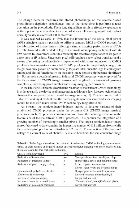
In the late 1990s it became clear that the roadmap of mainstream CMOS technology, in order to satisfy the device scaling according to Moore’s law, foresees technological changes that are partially detrimental to image sensing [5]. This is summarized in Table 8.1, making it evident that the increasing demands in semiconductor imaging cannot be met with mainstream CMOS technology long after 2000.
As a result, the semiconductor industry started to develop variants of their established CMOS processes under the acronym CIS (CMOS image sensing) processes. Such CIS processes continue to profit from the enduring reduction in the feature size of the mainstream CMOS processes. This permits the integration of a growing number of increasingly smaller pixels. The largest semiconductor image sensor fabricated to date contains the impressive number of 111 million pixels, while the smallest pixel pitch reported to date is 1.2 mm [6]. The reduction of the threshold voltage to a current value of about 0.3 V is also beneficial for semiconductor image
Table 8.1 Technological trends on the roadmap of mainstream CMOS technology, an evaluation (Eval) of their positive or negative impact on semiconductor imaging with these processes, and the main reason for this particular evaluation
CMOS technology trend Eval ReasonReduction of feature size ++ More pixels and functionality on chipReduction of threshold voltage + Higher signal levels and dynamic rangeReduction of power supply voltage + Reduced power consumption
− Lower signal levels and dynamic rangeGate material: poly-Si → silicides − Opaque gates in the visible spectrumSOI or epi-Si technology − Low red response and reduced QEIncrease of substrate doping − Larger dark currentIncrease of number of metal layers − “Tunnel vision”; low QE of small pixelsReduction of gate oxide thickness − − Larger dark current
8 Semiconductor Image Sensing 247
BookID 152004_ChapID 8_Proof# 1 - <Date>
sensors because the available voltage swing is increased. The reduction of the power supply voltage, however, is a mixed blessing: On one hand, power consumption is lowered appreciably, since it is proportional to the square of the supply voltage; on the other hand, this lowers also the voltage swing for representing photosignals and, as a consequence, also the dynamic range of the image sensor is reduced.
The replacement of doped polysilicon as the gate electrode material with silicides (CoSi
2 or TiSi
2) is beneficial since the gate’s electrical conductivity is improved but
since silicides are essentially opaque to visible radiation, photosensitive devices employing photogates lose much of their sensitivity. The replacement of bulk silicon with epitaxial silicon layers of a few micrometers thickness [as in silicon-on-insulator (SOI)] technology also reduces the sensitivity of photosensitive devices, in particular, in the red and near infrared spectral region where the penetration depth of light in silicon is particularly large. To enhance the electrical conductivity of the silicon substrate, doping levels of the implantations are increased to typical levels of about 1018 cm3. This implies a significant increase of the dark current density to values beyond 1 nA/cm2 at room temperature. Such values are clearly unacceptable in many imaging applications, in view of the low dark current densities of a few 10 pA/cm2 in commercially offered CIS processes and the record value of 0.6 pA/cm2 for the best CCD process.
The combination of shrinking pixel period and increasing number of metallization and via layers results in “chimney pixels,” as illustrated in Fig. 8.4, which at the same time reduces the optical sensitivity of the pixels and increases the angular
n+p-diodeM s
M rsel
M r
VDD
reset
Vout30 mm
row select
Fig. 8.4 Example of pixel layout for an active pixel sensor
dependence of their photoresponse. Finally, the reduction of the gate oxide thickness to today’s typical values of less than 2 nm increases the tunnel density current through the oxide to values exceeding 1 mA/cm2, which is clearly unacceptable in image sensing applications.
For these reasons, CIS processes are offered today that are derivatives of industrial CMOS processes, where all the problems mentioned earlier are addressed appropri-ately, and where great care is taken that the photosensitive devices can fully profit from the excellent optoelectronic properties of the silicon base material.
An example of pixel layout for a CMOS APS is given in Fig. 8.4. Because of the presence of circuitry within the pixel the area that is effectively sensitive to light is reduced to typically 25–65% of the total pixel area. This corresponds to the so-called fill factor. In comparison, CCDs typically have fill factors of 70–100% for full-frame CCD (FF-CCD) and frame transfer CCD (FT-CCD), whereas interline transfer CCDs (IT-CCD) achieve fill factors in the range of 25–30%.
A typical cross section of a pixel structure fabricated with such a commercially available CIS process is illustrated in Fig. 8.5. In the silicon substrate photosensitive regions are created using suitable implants: As detailed earlier, the preferred devices are photodiodes, buried (pinned) photodiodes, or CCD structures.
Oxide material is deposited on top of the silicon, containing the copper interconnects and vias, as well as the gate structures for the transistors. Different types of color filters are produced over the individual pixels, followed by microlens structures to enhance the effective light collection efficiency of the pixel. Their focusing effect is illustrated with the broken lines in Fig. 8.5, indicating schematically the ray tracing modeling that is necessary to optimize the optoelectronic performance of the pixels. Typical dimensions of state-of-the art CIS pixels as employed, for example, in
Fig. 8.5 Cross section of a typi-cal CIS pixel, consisting of a sili-con substrate with implanted photodiode regions, on top of which oxide material is deposited, where the copper interconnects, vias, gate structures, and color fil-ters are fabricated. To improve the light collection efficiency, a microlens array is produced
8 Semiconductor Image Sensing 249
BookID 152004_ChapID 8_Proof# 1 - <Date>
cost-effective image sensors used in mobile phone cameras are periods of 2–3 mm and a total thickness of 3–4 mm.
To produce more pixels for less money, the CIS industry will not cease to invest in the continuing reduction of pixel size. This involves solving the problem of reduced capacitance and reduced photosensitive surface of the ever-shrinking pixels: As an example, consider a pixel with a storage capacitance of 1.6 fF; assuming a maximum voltage swing of 1 V, such a pixel cannot store more than 10,000 electrons.
Since the photogenerated and stored charges show Poisson noise statistics, perceived picture quality deteriorates as a function of the stored photocharge numbers [7]. For this reason, good quality images require photocharge storage capacities of a few 10,000 electrons in each pixel. This problem is quite similar to the one in memory circuits: Despite the continuing reduction of the unit cell size, the capacitance of the unit storage cell must be kept at a certain value to assure reliable operation of the storage function. The solution adopted in CIS technology is, therefore, also related: The third dimension is exploited to increase the specific capacitance of pixel storage devices. An example of this development is the recently developed “stratified pinned photodiode,” realized by corrugating the outer shape of the buried photodiode implant [8].
The other problem of smaller pixels with increased “tunnel vision,” as illustrated in Fig. 8.5, is the reduced photosensitive surface and the increased angular dependence of the response. While microlenses can help to alleviate the problem, there will always remain an angular dependence of the pixel’s response, which reduces the pixel’s overall sensitivity, in particular when imaging lenses with small f# are employed. A promising technological approach to solve this problem is the separation of the optoelectronic transduction and the electronic circuitry into different layers. This is achieved by depositing a thin film of amorphous or microcrystalline silicon (or another suitable semiconductor) on top of an ASIC structure (TFA = thin film on ASIC technology). Photodiodes are fabricated in the top layer of TFA image sensors, and electrical connections to the charge sensing circuits on the ASIC are produced. In this way, an effective geometrical fill factor approaching 100% can be achieved, and the photoelectric conversion properties, including, for example, very low dark current, can be optimized separately from the ASIC in the thin film [9].
8.4 Examples and Applications of Imagers
8.4.1 Electronic Imaging in the Visible Spectrum
In the past, the main drivers of electronic imaging have been cost, performance, and functionality; without doubt, these drivers will stay unaffected in the foreseeable future. The challenge, therefore, is to take advantage of the continuing progress of
semiconductor physics to satisfy the demands of the market in terms of cost, performance, and functionality of the realized image sensors and camera systems.
8.4.1.1 Challenges and Opportunities
The key to meeting present-day challenge is integration: More electronic circuitry will be placed on each image sensor, and the pixels themselves will be supplied with all the analog and digital elements to improve their performance and to increase their functionality. Whenever economically justified, an application-specific single-chip digital camera (SoC=system-on-chip) will result that just needs to be complemented with inexpensive optics to arrive at a highly cost-effective solution.
A first huge, fast-growing, and highly contested market is electronic imaging for cell phones. It is estimated that close to one billion cell phone cameras will be sold in 2007. Consequentially, the price of such a complete single-chip digital camera has dropped to less than $5 in volume, while its resolution is already exceeding 1 megapixel. From this development, other mass markets such as automotive applications, game console interfaces, personal computer peripherals, and videoconferencing will surely profit. Typical single-chip camera developments for these and related applications where price is the main driver are described later.
Two other fast-growing markets with considerably higher margins are digital still cameras (DSC) and security/surveillance. Although both markets combined require only about 100 million image sensors in 2007 – slightly more than 10% of the cell phone camera market – the performance expectations of the customer are much higher: In the case of DSCs, multi-megapixel resolution (already exceeding 10 megapixels even for amateur cameras), high uniformity, and low noise are demanded. The performance expectations of the security/surveillance cameras are similar; however, the emphasis is not on the number of pixels but on the low-noise performance for low-light applications. The ultimate physical performance in this respect is single-photon resolution, and as soon as cost-effective solutions will be available, most other electronic imaging applications will demand such a performance, as well. The most promising approaches for low-light semiconductor image sensors are detailed later.
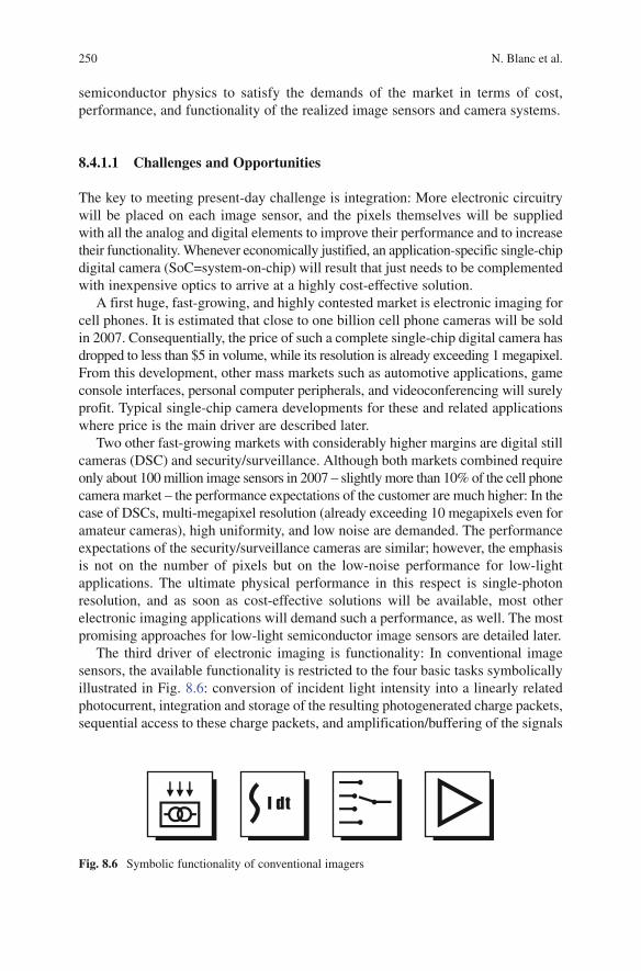
The third driver of electronic imaging is functionality: In conventional image sensors, the available functionality is restricted to the four basic tasks symbolically illustrated in Fig. 8.6: conversion of incident light intensity into a linearly related photocurrent, integration and storage of the resulting photogenerated charge packets, sequential access to these charge packets, and amplification/buffering of the signals
Fig. 8.6 Symbolic functionality of conventional imagers
8 Semiconductor Image Sensing 251
BookID 152004_ChapID 8_Proof# 1 - <Date>
to make them available off chip. By complementing this basic optoelectronic functionality with analog and digital circuit building blocks, in each pixel or adjacent to the pixel matrix, a very rich toolbox for the realization of application-specific “smart image sensors” is created. Some of this additional functionality, all fabricated with the technological capabilities of the same CIS process, is schematically illustrated in Fig. 8.7, indicating the broad range of building blocks available for the design of custom imagers. This includes, among other things, smart pixels with nonlinear response for a dynamic range approaching 200 dB, color pixels making use of the wavelength-dependent absorption of silicon, pixels with unusual geometries implementing selected linear or nonlinear transforms, in-pixel analog processing circuits for basic arithmetic operations in the photocharge domain, as well as conventional analog and digital circuits in the pixels or as complementary building blocks beside the photosensor area on the image sensor [10].
The availability of this toolbox of functionality is the key for improving the performance of novel, smart pixels over previous types of pixels, and for providing the custom functionality required for the successful integration of special image sensors for a large variety of applications.
As detailed later, this development is expected to culminate in the realization of complete single-chip machine vision systems, so-called “seeing chips.”
Σ
l+–
Fig. 8.7 Symbolic illustration of a few examples of functional building blocks available for smart pixels and custom image sensors
The continuous trend toward miniaturization and higher density in CMOS mixed-signal technologies has a strong impact on the development and progress in solid-state image sensors and related applications. Whereas image sensors based on a passive MOS (metal oxide semiconductor) array architecture were already demonstrated in the seventies, their noise figures and overall performances turned out to be by far not sufficient to compete with dedicated CCD-based imaging products. It is only with the introduction of the APS concept in the nineties that CMOS imagers have been able to step by step close the gap with CCD imagers. The main improvement came with the capability to integrate active transistors within every pixel of the imager in order to locally amplify the typically very small photogenerated signals. This approach basically reduces significantly the large stray capacitances that characterize passive MOS array imager to a few tens of fF, i.e., values similar to the input capacitance of CCDs’ output stages. The use of more aggressive technologies and submicron processes was thus instrumental for the performance improvements of CMOS imagers. Furthermore, the use of standard CMOS technologies opens up the possibility of manufacturing imaging devices that can be monolithically integrated: functions such as timing, exposure control, and analog to digital conversion (ADC) can be implemented on one single piece of silicon, enabling the production of single-chip digital image sensors. With ever decreasing transistor size, it also becomes technically and economically possible to combine the image sensor with functions such as digital signal processor, microcontroller, or further interfaces (e.g., USB). Clearly the higher number of pixels that can be integrated on ever decreasing areas have fuelled the success of CMOS imagers. As such, to a large part, the success of single-chip digital cameras can be seen as a direct result of “more Moore.”
Today solid-state cameras have become pervasive tools in many markets. It is forecast already that next year more than a billion solid-state imagers will be sold worldwide, the dominating applications and markets being mobile phones, digital still photography, security, automotive, and toys. CMOS technologies and in particular CMOS imagers have also intrinsically the potential for lower power consumption. CMOS imagers can be driven from one single supply voltage (typically <3.3 V) and with power consumption below a few tens of mW making these devices particularly attractive for mobile applications, such as the mobile phone market. The latter market corresponds today to roughly 50% of the units sold worldwide.
Low power consumption also helps to reduce the temperature (or temperature gradient) of the sensor chip and camera head, leading in general to improved performances. Figure 8.8 shows a single-chip digital camera with a spatial resolution of 176 × 144 pixels. It operates at 1.5 V and consumes less than 1 mW [14]. The low power consumption is achieved by the reduction in the power supply voltage and by applying special techniques for the analog design. Sensors operating at less than 1 mW have also been demonstrated [15]. Video cameras in mobile phone have become a reality today. Undoubtedly further applications, for example,
8 Semiconductor Image Sensing 253
BookID 152004_ChapID 8_Proof# 1 - <Date>
in medicine (e.g., minimally invasive medicine/endoscopy) or surveillance and security, will profit from the progress made in low-power digital imaging.
8.4.1.3 High-Sensitivity Electronic Imaging, Single-Chip Digital Low-Power Camera
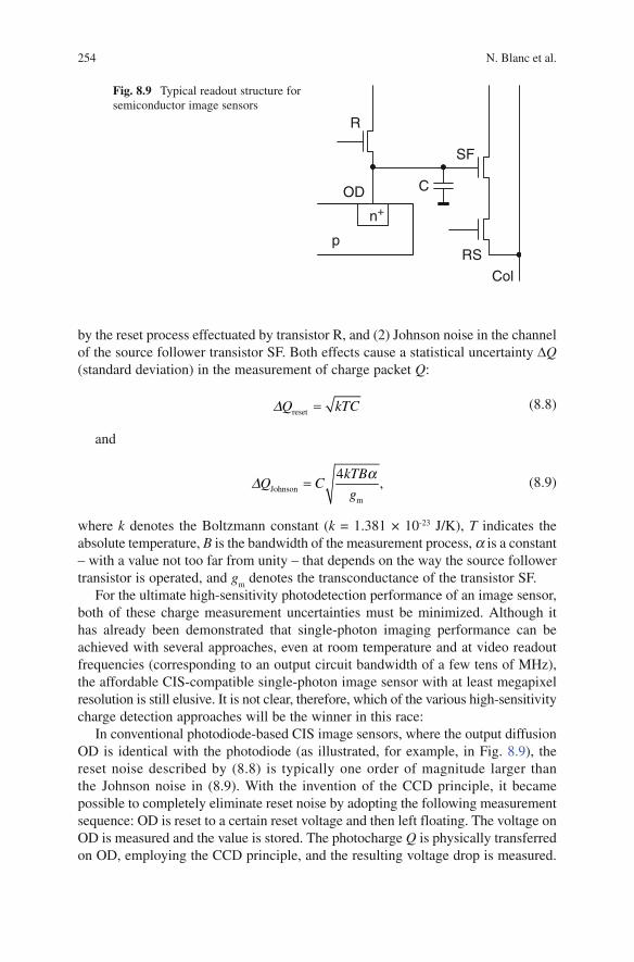
As we have seen in Sect. 2, the external quantum efficiency of silicon can be close to 100% in the visible spectral domain (for monochrome imaging). Since this means that almost each incident photon is converted into an electron–hole pair, the physical problem of high-sensitivity image sensing is really an electronic problem of high-sensitivity charge sensing. The electronic photocharge detection circuit used almost exclusively in semiconductor image sensing is illustrated in Fig. 8.9: In a p substrate, an n+ output diffusion (OD) is implanted. Using the reset transistor R, this diffusion is reverse-biased to a certain reset potential, and it is left floating afterward. The photocharge Q that should be measured is then placed on OD, lowering its potential by the amount V = Q/C, where C indicates the total effective capacitance at the gate of the source follower transistor SF. The voltage at C in each pixel can be measured individually by connecting SF with the row-select transistor RS to the column signal line Col, which terminates in a load transistor for SF.
Two noise sources dominate the charge measurement process in the source follower circuit shown in Fig. 8.9: (1) Reset noise – also called kTC noise – introduced
Pixel array(356 x 292)
Prog. gain amplifiers22 SAR ADCs
Control logic
2mW
Fig. 8.8 Micrograph of a digital single-chip camera with a power consumption of less than 2 mW
by the reset process effectuated by transistor R, and (2) Johnson noise in the channel of the source follower transistor SF. Both effects cause a statistical uncertainty DQ (standard deviation) in the measurement of charge packet Q:
resetQ kTCD = (8.8)
and
Johnsonm
4,
kTBQ C
g
aD =
(8.9)
where k denotes the Boltzmann constant (k = 1.381 × 10⁻²³ J/K), T indicates the absolute temperature, B is the bandwidth of the measurement process, a is a constant – with a value not too far from unity – that depends on the way the source follower transistor is operated, and g
m denotes the transconductance of the transistor SF.
For the ultimate high-sensitivity photodetection performance of an image sensor, both of these charge measurement uncertainties must be minimized. Although it has already been demonstrated that single-photon imaging performance can be achieved with several approaches, even at room temperature and at video readout frequencies (corresponding to an output circuit bandwidth of a few tens of MHz), the affordable CIS-compatible single-photon image sensor with at least megapixel resolution is still elusive. It is not clear, therefore, which of the various high-sensitivity charge detection approaches will be the winner in this race:
In conventional photodiode-based CIS image sensors, where the output diffusion OD is identical with the photodiode (as illustrated, for example, in Fig. 8.9), the reset noise described by (8.8) is typically one order of magnitude larger than the Johnson noise in (8.9). With the invention of the CCD principle, it became possible to completely eliminate reset noise by adopting the following measurement sequence: OD is reset to a certain reset voltage and then left floating. The voltage on OD is measured and the value is stored. The photocharge Q is physically transferred on OD, employing the CCD principle, and the resulting voltage drop is measured.
n+
p
R
SF
C
RS
Col
OD
Fig. 8.9 Typical readout structure for semiconductor image sensors
8 Semiconductor Image Sensing 255
BookID 152004_ChapID 8_Proof# 1 - <Date>
The difference of these two measurements results in a voltage value that is linearly related to the photocharge Q, and its statistical uncertainty DQ is reduced to the Johnson noise described in (8.9).
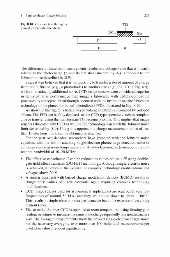
Since it was believed that it is not possible to transfer a stored amount of charge from one diffusion (e.g., a photodiode) to another one (e.g., the OD in Fig. 8.9), without introducing additional noise, CCD image sensors were considered superior in terms of noise performance than imagers fabricated with CMOS-compatible processes. A conceptual breakthrough occurred with the invention and the fabrication technology of the pinned (or buried) photodiode (PPD), illustrated in Fig. 8.10.
As shown in this figure, a buried n-type volume is entirely surrounded by p-doped silicon. This PPD can be fully depleted, so that CCD-type operations such as complete charge transfer using the transfer gate TG become possible. This implies that image sensors fabricated with CCD as well as CIS technology can reach the Johnson noise limit described by (8.9). Using this approach, a charge measurement noise of less than 10 electrons r.m.s. can be obtained in practice.
For the past two decades, researchers have grappled with the Johnson noise equation, with the aim of attaining single-electron photocharge detection noise in an image sensor at room temperature and at video frequencies (corresponding to a readout bandwidth of 10–20 MHz):
• The effective capacitance C can be reduced to values below 1 fF using double-gate field-effect transistor (DG-FET) technology. Although single-electron noise is achieved, it comes at the expense of complex technology modifications and voltages above 20 V.
• A similar approach with buried charge modulation devices (BCMD) results in charge noise values of a few electrons, again requiring complex technology modifications.
• CCD image sensors used for astronomical applications are read out at very low frequencies of around 50 kHz, and they are cooled down to about −100°C. This results in single-electron noise performance but at the expense of very long readout times.
• The so-called Skipper CCD is operated at room temperature, using floating gate readout structures to measure the same photocharge repeatedly in a nondestructive way. The averaged measurements show the desired single-electron charge noise but the necessary averaging over more than 100 individual measurements per pixel slows down readout significantly.
TG
n+
p
Ox
p+
n
Se
Fig. 8.10 Cross section through a pinned (or buried) photodiode
• To circumvent the problem of noisy electronic charge detection, physical amplification mechanisms with low excess noise factors are actively pursued. Image sensors with APDs, either working in the linear or in the Geiger mode, have been realized, exhibiting the wanted single-electron charge noise at room temperatures and at video frequency readouts. Several products such as the Impactron™ CCD image sensor with avalanche amplification section, developed by Texas Instruments, are offered commercially. Unfortunately, the high electric fields required to cause avalanche amplification still necessitate voltages of 20 V and more, making the use of avalanche-based single-electron imagers somewhat unpractical.
• Probably the most promising approach for cost-effective single-electron image sensors is “bandwidth engineering”: The measurement bandwidth B in (8.9) is significantly reduced, either at each pixel site or in each column amplifier. Suitable imager architectures with parallel readout capabilities provide for data readout at unimpeded speeds, despite the low-pass filtering effect; for example, see [11]. The large advantage of this approach is its entire compatibility with standard CIS technology, as well as low-power, low-voltage operation.
None of these approaches has yet resulted in the commercial availability of cost-effective, easy-to-use image sensors with close to single-photon performance. Without doubt, such devices, based on one of the described principles, will become available in the next few years.
Pixel dimension reduction is justified not only to decrease the costs, following the Moore’s law trend, but also to reduce the volume and thickness of the imager including its optical part. The reason is that for a given optical f#, a reduction of the lens diameter results in a reduction of the focal length and hence the total thickness of the imager. The main drawbacks of this trend concern the optics, with diffraction effects close to the pixel pitch, and the pixel collected charge possibilities, reduced as the pixel size is lowered. The drastic size reduction of the well collecting the photogenerated electrons, able to collect typically 40,000 e− with 16 mm in pitch pixel, 10,000 e− with 2.2 mm, and 6,000 e− with 1.45 mm, is the strong motivation to decrease the total noise coming with each pixel reading: the dynamic range being reduced with its upper limit, the lower limit must improve drastically. The best read noise results are now in the range of 1–2 electrons RMS. Nevertheless, even with a low noise reading, the fluctuations of number of photogenerated electrons are correlated with a Poisson distribution, which predicts a RMS value given by the square root of the total electrons number. This phenomenon comes from the photon number statistical fluctuation and cannot be avoided without increasing the total number of collected electrons. To obtain a SNR (signal-to-noise ratio) of 10, 100 photogenerated electrons are necessary with a perfect nonnoisy reading circuit. To increase this collection number, several directions are to be considered.
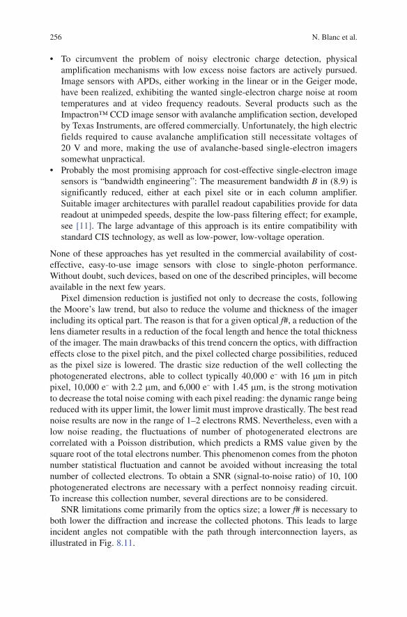
SNR limitations come primarily from the optics size; a lower f# is necessary to both lower the diffraction and increase the collected photons. This leads to large incident angles not compatible with the path through interconnection layers, as illustrated in Fig. 8.11.
8 Semiconductor Image Sensing 257
BookID 152004_ChapID 8_Proof# 1 - <Date>
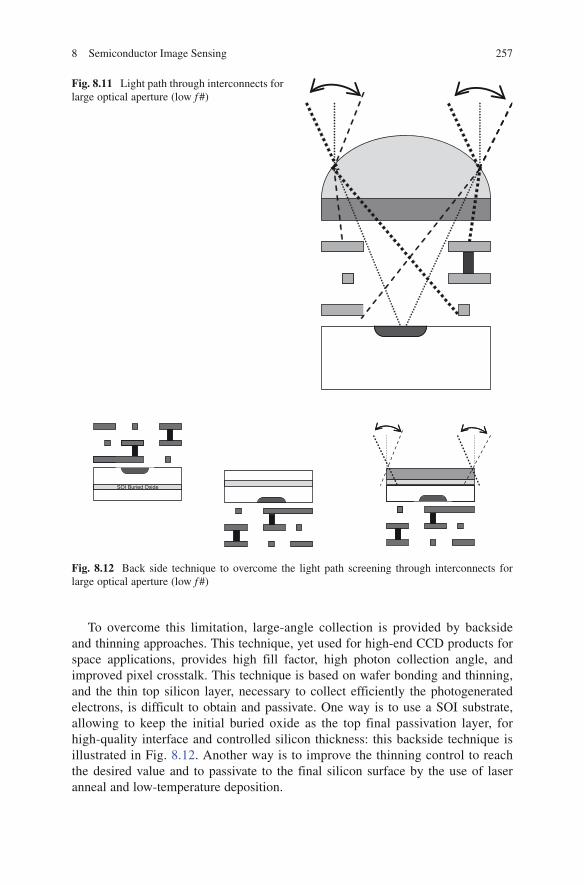
To overcome this limitation, large-angle collection is provided by backside and thinning approaches. This technique, yet used for high-end CCD products for space applications, provides high fill factor, high photon collection angle, and improved pixel crosstalk. This technique is based on wafer bonding and thinning, and the thin top silicon layer, necessary to collect efficiently the photogenerated electrons, is difficult to obtain and passivate. One way is to use a SOI substrate, allowing to keep the initial buried oxide as the top final passivation layer, for high-quality interface and controlled silicon thickness: this backside technique is illustrated in Fig. 8.12. Another way is to improve the thinning control to reach the desired value and to passivate to the final silicon surface by the use of laser anneal and low-temperature deposition.
Fig. 8.11 Light path through interconnects for large optical aperture (low f #)
SOI Buried OxideSOI Buried Oxide
Fig. 8.12 Back side technique to overcome the light path screening through interconnects for large optical aperture (low f #)
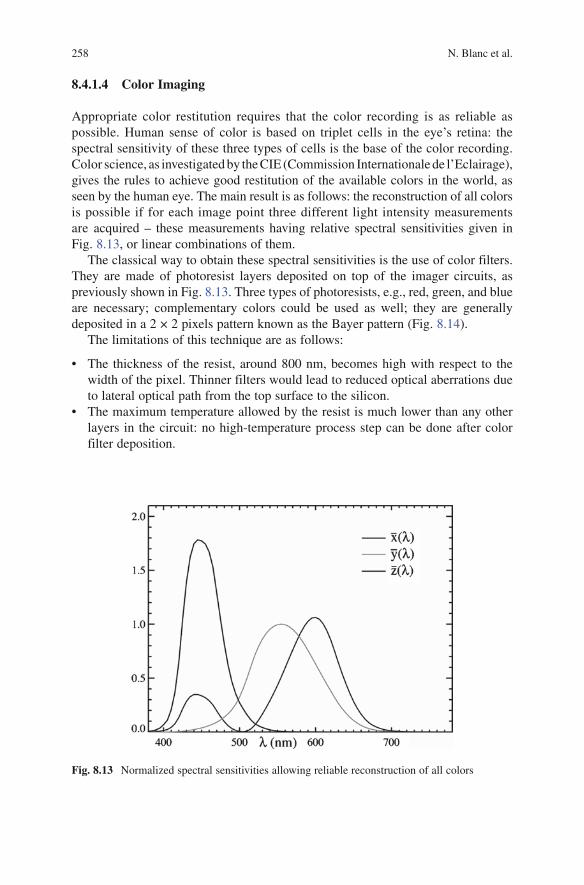
Appropriate color restitution requires that the color recording is as reliable as possible. Human sense of color is based on triplet cells in the eye’s retina: the spectral sensitivity of these three types of cells is the base of the color recording. Color science, as investigated by the CIE (Commission Internationale de l’Eclairage), gives the rules to achieve good restitution of the available colors in the world, as seen by the human eye. The main result is as follows: the reconstruction of all colors is possible if for each image point three different light intensity measurements are acquired – these measurements having relative spectral sensitivities given in Fig. 8.13, or linear combinations of them.
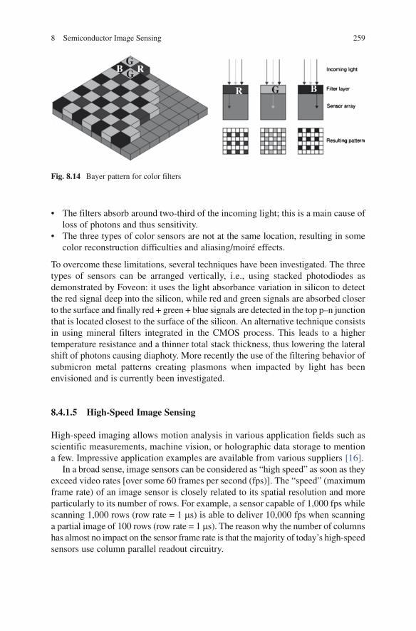
The classical way to obtain these spectral sensitivities is the use of color filters. They are made of photoresist layers deposited on top of the imager circuits, as previously shown in Fig. 8.13. Three types of photoresists, e.g., red, green, and blue are necessary; complementary colors could be used as well; they are generally deposited in a 2 × 2 pixels pattern known as the Bayer pattern (Fig. 8.14).
The limitations of this technique are as follows:
• The thickness of the resist, around 800 nm, becomes high with respect to the width of the pixel. Thinner filters would lead to reduced optical aberrations due to lateral optical path from the top surface to the silicon.
• The maximum temperature allowed by the resist is much lower than any other layers in the circuit: no high-temperature process step can be done after color filter deposition.
Fig. 8.13 Normalized spectral sensitivities allowing reliable reconstruction of all colors
8 Semiconductor Image Sensing 259
BookID 152004_ChapID 8_Proof# 1 - <Date>
• The filters absorb around two-third of the incoming light; this is a main cause of loss of photons and thus sensitivity.
• The three types of color sensors are not at the same location, resulting in some color reconstruction difficulties and aliasing/moiré effects.
To overcome these limitations, several techniques have been investigated. The three types of sensors can be arranged vertically, i.e., using stacked photodiodes as demonstrated by Foveon: it uses the light absorbance variation in silicon to detect the red signal deep into the silicon, while red and green signals are absorbed closer to the surface and finally red + green + blue signals are detected in the top p–n junction that is located closest to the surface of the silicon. An alternative technique consists in using mineral filters integrated in the CMOS process. This leads to a higher temperature resistance and a thinner total stack thickness, thus lowering the lateral shift of photons causing diaphoty. More recently the use of the filtering behavior of submicron metal patterns creating plasmons when impacted by light has been envisioned and is currently been investigated.
8.4.1.5 High-Speed Image Sensing
High-speed imaging allows motion analysis in various application fields such as scientific measurements, machine vision, or holographic data storage to mention a few. Impressive application examples are available from various suppliers [16].
In a broad sense, image sensors can be considered as “high speed” as soon as they exceed video rates [over some 60 frames per second (fps)]. The “speed” (maximum frame rate) of an image sensor is closely related to its spatial resolution and more particularly to its number of rows. For example, a sensor capable of 1,000 fps while scanning 1,000 rows (row rate = 1 ms) is able to deliver 10,000 fps when scanning a partial image of 100 rows (row rate = 1 ms). The reason why the number of columns has almost no impact on the sensor frame rate is that the majority of today’s high-speed sensors use column parallel readout circuitry.
The highly parallel architecture of CMOS sensors has led within the last decade to a technology shift from CCDs toward CMOS imagers for high-speed imaging. For low spatial resolution in turn, CCD sensors are still capable of recording high speeds, which have by far not been equaled by CMOS. As a comparison, a 320 × 260 pixel CCD sensor using in situ storage is capable of 1 M (106) fps [17], while a 352 × 288 pixel CMOS sensor using innovative in situ ADCs reaches 10k (104) fps [18]. For higher spatial resolution (and lower speed) CMOS image sensors (CIS) have, however, overtaken the market place. This success is mainly attributable to the system integration capability of CIS, which leads to lower cost cameras. Up to the 1990s, CCD and early CIS [19] delivered analog output and thus A/D conversion had to be performed in separate ICs. With the advent in the late 1990s of the first on-chip column-parallel ADCs [20], the way was paved for implementing high-speed/high-resolution digital imagers [21]. Today, a typical 1.3-megapixel high-speed sensor delivers 500 fps at full resolution [22].
To speed-up image acquisition, high-speed sensors use snap-shoot pixels operat-ing in the “integrate-while-read” (IWR) mode of operation. IWR-capable pixels do per definition require in-situ storage, a property that was interestingly also required in the very first CMOS photodiode array published in the early 1990s [23]. Therefore, the same 5T pixels were reused [19] and fine-tuned for improved responsivity [24], one of the key requirements to the sensing part of a high-speed sensor, since high frame rates imply short integration time. To improve the sensitivity at pixel level, the conversion factor (CF) must be maximized, e.g., the capacitance of the photodiode and floating diffusion must be minimized. With the 3-µm process in the early 1990s, C
d and C
FD were in the order of 50 fF [23], yielding a poor CF
of ~1.6 mV/e. With a modern 0.25-µm process, a CF of 13 mV/e is typical [22], meaning that C
d and C
FD have been lowered to some 6 fF. Various pixels with
improved sensitivity have been proposed by either incorporating an amplifier in front of the shutter [25–27] or an in-pixel charge amplifier [28]. The first approach improves CF by a factor of 2 (~20 mV/e), while the second allows boosting the CF to some 38 mV/e. With the advent of pinned photodiode, the CF of traditional 5T pixels improves by a factor of 2, which allows smaller pixels [29] to rival with more complicate ones in term of CF. In addition to CF improvement at pixel level, almost all sensors further increase the overall sensitivity by electronic gain boosting inside the column amplifier (prior to A/D conversion).
Three types of column-parallel ADCs are used in today’s CIS: single-slope, successive-approximation (SA), and cyclic/pipeline converters. Single slope converters are widely used in low-speed imagers. Recently, however, such an ADC has been pushed to a remarkable speed of 180 fps at 1,440 rows (row-rate = 3.86 ms) for 10 bits by using a 300-MHz clock [30]. Sensors with higher throughput usually use SA-ADCs, which typically reach 5,000 fps at 512 rows (row rate = 0.39 ms) [24] or 440 fps at 1,728 rows (row rate = 1.3 ms) [31] for 10 bits. It is difficult to achieve more than 10-bit gray-scale resolution with SA-ADCs on CIS. To increase the ADC resolution, the authors of [28] have developed cyclic converters capable of 3,500 fps at 512 rows (row rate = 0.56 ms) for 12 bits. Other publications have reported the use of multiplexed pipeline converters [27] [32] with similar
8 Semiconductor Image Sensing 261
BookID 152004_ChapID 8_Proof# 1 - <Date>
aggregate performances as early-day SA-ADCs (500 fps at 1,024 rows/2 ms row rate for 10 bits [21, 32]).
High-speed digital CIS produce tremendous amounts of data: for example, the 440-fps 4.1-megapixel sensor of [31] delivers 18 Gbit/s (4.1 megapixels × 440 fps × 10 bit), which are dumped into some external IC over 160 pins toggling at 120 MHz. Such I/O bandwidths are indeed quite challenging to handle both at IC level (large power consumption, on-chip noise) and at board level (large buses, signal integrity). Some newer designs thus propose LVDS outputs [27, 32, 33] to solve those issues. Recently, incorporation of on-chip parallel image compression circuits for reducing the data traffic has been proposed [34]. In a prototype 3,000-fps sensor, a compression ratio of 4.5 has been demonstrated.
In future, further functionality will be integrated onto CIS dies. An example of such a sensor using programmable single-instruction multiple data-stream (SIMD) parallel digital processing has been published in [35]. The IC, aimed at high-speed machine vision, combines image acquisition, digitalization, and column-parallel SIMD processing with a computational power of 100 GOPS. With the availability of sub 100 nm mixed DRAM/imager technology, integration of a frame memory will also become economically viable [34].
8.4.1.6 Optical Time-of-Flight 3D Cameras
Humans are capable of perceiving their environment in three dimensions. This key capability represents in turn a major challenge to film-based and electronic camera systems. In fact, so far, cameras have been typically optimized for, and also limited to, the acquisition of two-dimensional images, providing basically only monochrome or color images without any direct information on depth. The race for higher (lateral) spatial resolution continues unabatedly; today’s still picture cameras for the consumer market offer resolution in excess of 10 megapixels, whereas scientific and professional cameras already count more than a few tens of megapixels. This race for more pixels is very reminiscent of the continuous trends toward a higher degree of integration, a higher number of transistors as described by “more Moore.” In contrast the shift from 2D imaging toward real-time 3D imaging represents a major technological step and paradigm change. A new type of information is available, based on sensors and pixels with added functionality – thanks to processing capabilities (at the pixel level). These smart sensors and pixels can be seen as vivid examples of “more than Moore.” It also opens up completely new application opportunities in numerous fields such as in security, in automotive, in industrial control and machine vision, in the medical sector as well as in consumer electronics and mobile robots. All these applications can very directly benefit from camera systems that are able to capture the world in real time and in all three dimensions. This is particularly true if such 3D systems can be made compact, robust, and cost-effective. The technological requirements for such 3D systems are nevertheless stringent: To a large extent obtaining reliable real-time distance information over an entire scene is indeed very challenging and originally distance measuring systems
have been limited to point measurements or to scanning systems, the latter being rather slow and/or expensive. Over the last few years however, technological progress in semiconductor devices and microtechnologies has lead to sensors that can “see distances” within complete scenes at affordable prices [36–39]. The breakthrough came with a new type of optical 3D camera based on the time-of-flight principle that uses the finite velocity of light (c = 3 × 10⁸ m/s) to measure distances. Either a pulse or a continuously modulated light wave is sent out by an illumination module. Correspondingly, either the “time of flight” t, which is the time the light needs to travel from the illumination module to the target and back to the sensor, or the phase delay ø of the continuously modulated light wave for this round trip is used to calculate distances within a scene. The latter method, referred as continuous wave (CW) modulation presents several advantages over the light pulse technique. In particular, the requirements to the illumination module and the electronics are not so demanding. Short optical pulses require a high optical power and a high bandwidth of the electronic components. In the CW modulation scheme, light from a LED or laser diode array is modulated to a frequency f
mod of a few tens of MHz and
illuminates the scene. The light that is reflected back by the objects and/or persons in the scene is imaged with a lens onto a custom solid-state image sensor. Each of the pixels of this sensor is capable of synchronous demodulation of the incident modulated light for the precise local determination of the phase delay. From the phase delay ø, distances can be computed directly as given by the following equation.
0( ) e .xI x I a-= (8.10)
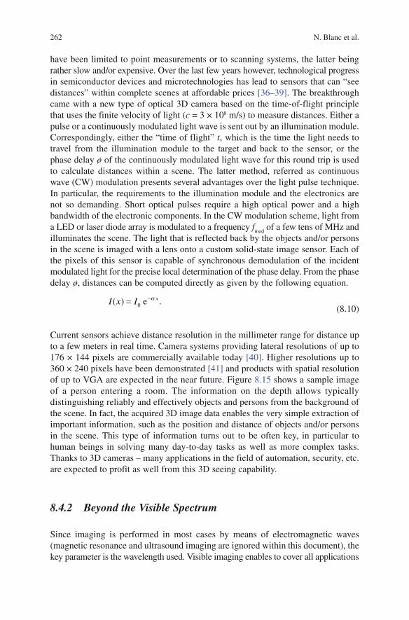
Current sensors achieve distance resolution in the millimeter range for distance up to a few meters in real time. Camera systems providing lateral resolutions of up to 176 × 144 pixels are commercially available today [40]. Higher resolutions up to 360 × 240 pixels have been demonstrated [41] and products with spatial resolution of up to VGA are expected in the near future. Figure 8.15 shows a sample image of a person entering a room. The information on the depth allows typically distinguishing reliably and effectively objects and persons from the background of the scene. In fact, the acquired 3D image data enables the very simple extraction of important information, such as the position and distance of objects and/or persons in the scene. This type of information turns out to be often key, in particular to human beings in solving many day-to-day tasks as well as more complex tasks. Thanks to 3D cameras – many applications in the field of automation, security, etc. are expected to profit as well from this 3D seeing capability.
8.4.2 Beyond the Visible Spectrum
Since imaging is performed in most cases by means of electromagnetic waves (magnetic resonance and ultrasound imaging are ignored within this document), the key parameter is the wavelength used. Visible imaging enables to cover all applications
8 Semiconductor Image Sensing 263
BookID 152004_ChapID 8_Proof# 1 - <Date>
where the information needs to be closed to the human vision. Beyond the visible spectrum, X-ray, infrared, and Terahertz electromagnetic waves are of most interest in many applications.
8.4.2.1 Challenges and Opportunities
Medical imaging, for example, is accomplished by means of X-ray, gamma rays (in nuclear medicine), visible light (ocular fundus, skin), infrared light (mamma transillumination), or even Terahertz waves, which has been proposed recently. In X-ray imaging, the gold standard is the X-ray-based mammography, where a special radiographic unit is used. Optical imaging of the retina is the only way to examine veins directly and noninvasively. Tele-ophthalmology has been demonstrated in a large international project.
As for medical imaging, industrial control and surveillance applications really take the benefit from detector innovations for X-ray range (e.g., CdTe material developments and new hybridization technics), infrared technologies (continuous need for improvement to decrease price), and new terahertz technologies
8.4.2.2 X-ray Imaging
Today X-ray imaging is used in many domains: medical, nondestructive testing, and security check. Most of the new developments are currently driven by medical requirements. This paragraph aims at giving a specific focus on medical image sensors.
Fig. 8.15 Sample image of 3D data (with permission of Mesa Imaging) [40]
First based on films, in the 1970s analog fluoroscopy became widely used. This modality was realized by an X-ray image-intensifier tube coupled to a TV camera. Sometimes, this kind of system was also used to take single images where the image resolution, however, was limited by the camera performance. In the 1980s, X-ray radiography became digital by introducing the so-called computed radiography where a storage phosphor in a cassette is irradiated and later on read out by a laser scanner.
State-of-the-art all-digital X-ray imaging is accomplished by flat-panel detectors [43]. These detectors are based on a large-area semiconductor film, i.e., hydrogenated amorphous silicon (a-Si), forming an array of thin-film transistors (TFT) managing readout of the picture elements. The fundamental interaction of the electromagnetic radiation with the material is the absorption. It is dependent on the energy. Secondary effects are called reflection scattering diffraction and refraction. All these interactions can be studied with Monte Carlo simulations. Details of interest differ from the surrounding tissues. This results in the contrast. To “see” its amplitude it needs to be compared with image noise.
The total image noise includes the detector noise and it is still of most interest to work on the performance of those X-ray image sensors.
Current Digital X-ray Image Sensors
Current digital X-ray imagers are FD detectors (flat panel solid-state detectors), and they are suitable for most X-ray imaging applications. They are based on an amorphous silicon a-Si readout matrix; each pixel comprises an a-Si switch and a sensing element. The restricted space limits the resolution to a minimum pitch of 70 mm.
For better resolution, the most advanced X-ray image sensors are CCD or CMOS based. The pixel size can be as low as 10 mm × 10 mm. These image sensors are responsive in the visible range. For X-ray imaging, the conversion from X-rays to light is performed by a scintillator bound to a fiberoptic face plate. This configuration leads to the best resolution (better than 20 lp/mm).
Large surfaces up to 49 mm × 86 mm are currently commercialized. However, CCDs and CMOS are there at their limits and increasing the surface in such technologies is hardly compatible with reasonable production cost.
For large field of view X-ray imaging such as mammography, chest… it is important to work on new large sensors.
New Image Sensor Concepts
In recent years, several advanced imaging solutions have been realized or currently are under development. In the following, some of these technologies are presented.
CCD-based detectors for very high spatial resolution: As mentioned earlier, FD detectors are suitable for most X-ray imaging applications. They are based on an
8 Semiconductor Image Sensing 265
BookID 152004_ChapID 8_Proof# 1 - <Date>
a-Si readout matrix, each pixel comprising an a-Si switch and a sensing element. The restricted space available leads to a minimum pixel pitch of some 70 mm; otherwise, the spatial fill factor of the pixels would become too low. Especially for mammographic biopsies imaging with very high resolution is desirable. Therefore, a CCD-based detector has been developed with a pixel pitch of 12 mm. It can be also used in a 2 × 2 or 4 × 4 binned mode, resulting in 24 or 48-mm pixels, respectively. The detector uses a CsI scintillator that is coupled via a fiberoptic plate to the sensor with 4k × 7k pixels. The sensitive area is 49 mm × 86 mm being the largest CCD in serial production in the world [49].
CdTe is also a material of choice. Up to now, price versus performance was questionable, but current R&D works performed on both the material growth (in order to improve the yield and size) and on hybridization technics (in order to decrease the pitch and hybridization cost) give good results and open new perspectives for this material (such as X-ray intraoral application) for medium-size imaging. This technology should increase drastically the contrast on the image and aim at being compatible with market price.
Organic semiconductor-based detectors: Current FD detectors are based on a-Si technology that has proven to be suitable for radiological, fluoroscopic, and angiographic applications. These detectors are built on glass substrates, which are rigid, heavy, and fragile. The a-Si layers and electrodes are patterned by photoli-thography, a process enabling the production of fine structures. Depositing a-Si requires elevated temperatures in the order of 250°C. In summary, there is also a demand for cheaper alternatives to a-Si technology.
Some investigations are going on into all-organic detectors [50]. Plastic substrates can be used that are flexible, lightweight, and unbreakable. The organic semiconductor and electrode layers can be deposited in the desired pattern, e.g., by jet printing. This results in cheap detectors that have the potential for new applications. Since an organic detector is not as heavy as an a-Si-based detector, it lends itself to use in a portable bedside device.
It has been shown that organic photodiodes and transistors are feasible, but further work is necessary to improve their performance.
8.4.2.3 Infrared Image Sensors
Today thousands of cooled IR detectors are produced taking advantage of the good know-how regarding this domain [57–60]. However, these current IR detectors have some limitations regarding their ability to operate in all weather conditions, and in terms of compactness and reliability. Therefore, research for moving to the next generation of detectors is in progress to overcome these limitations as well as to offer more performance. In parallel, the production cost reduction is one of the main challenges for cooled IR detectors, and new technologies are developed to answer this need.
These new researches and developments are dedicated to smaller pixel pitches, large formats, APDs, multicolor detectors, and active imagery detector needs as
well as optimization of microbolometer technology, one of the best choices for compactness/very low price compromise. This technology still requires miniaturization but is very promising and should open new applications in volume markets such as automobile and energy monitoring in buildings.
Infrared Detector Development
A lot of different technologies and sensitive materials are well mastered and available for IR detector production. As a matter of fact, quantum well IR photo-detectors (QWIP) have been developed [ex Thales Research and Technologies (TRT)] and are at mass production level in cooperation with Sofradir. Then, InSb technologies are also available.
As to HgCdTe technologies, they have been widely used for high-performance IR detectors and are at mass level production for years. Finally uncooled technology was developed based on amorphous silicon microbolometers at CEA Leti. Then it was transferred to ULIS (the subsidiary of Sofradir) and is at mass production level since 2003. In addition, other developments are running like InGaAs technology in Xenics and III–V lab.
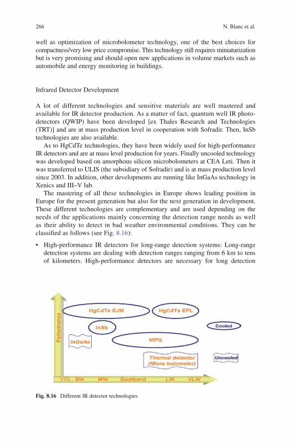
The mastering of all these technologies in Europe shows leading position in Europe for the present generation but also for the next generation in development. These different technologies are complementary and are used depending on the needs of the applications mainly concerning the detection range needs as well as their ability to detect in bad weather environmental conditions. They can be classified as follows (see Fig. 8.16):
• High-performance IR detectors for long-range detection systems: Long-range detection systems are dealing with detection ranges ranging from 6 km to tens of kilometers. High-performance detectors are necessary for long detection
Fig. 8.16 Different IR detector technologies
8 Semiconductor Image Sensing 267
BookID 152004_ChapID 8_Proof# 1 - <Date>
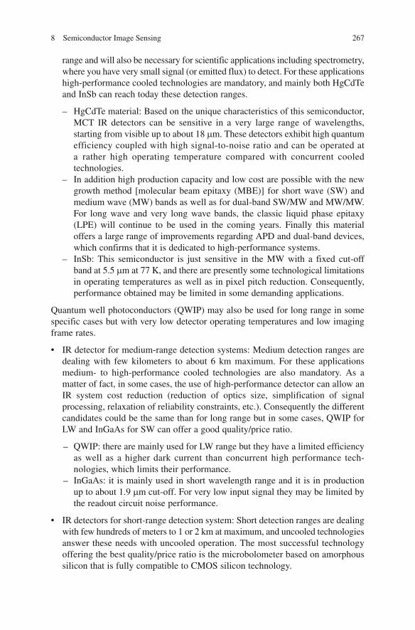
range and will also be necessary for scientific applications including spectrometry, where you have very small signal (or emitted flux) to detect. For these applications high-performance cooled technologies are mandatory, and mainly both HgCdTe and InSb can reach today these detection ranges.
– HgCdTe material: Based on the unique characteristics of this semiconductor, MCT IR detectors can be sensitive in a very large range of wavelengths, starting from visible up to about 18 mm. These detectors exhibit high quantum efficiency coupled with high signal-to-noise ratio and can be operated at a rather high operating temperature compared with concurrent cooled technologies.
– In addition high production capacity and low cost are possible with the new growth method [molecular beam epitaxy (MBE)] for short wave (SW) and medium wave (MW) bands as well as for dual-band SW/MW and MW/MW. For long wave and very long wave bands, the classic liquid phase epitaxy (LPE) will continue to be used in the coming years. Finally this material offers a large range of improvements regarding APD and dual-band devices, which confirms that it is dedicated to high-performance systems.
– InSb: This semiconductor is just sensitive in the MW with a fixed cut-off band at 5.5 mm at 77 K, and there are presently some technological limitations in operating temperatures as well as in pixel pitch reduction. Consequently, performance obtained may be limited in some demanding applications.
Quantum well photoconductors (QWIP) may also be used for long range in some specific cases but with very low detector operating temperatures and low imaging frame rates.
• IR detector for medium-range detection systems: Medium detection ranges are dealing with few kilometers to about 6 km maximum. For these applications medium- to high-performance cooled technologies are also mandatory. As a matter of fact, in some cases, the use of high-performance detector can allow an IR system cost reduction (reduction of optics size, simplification of signal processing, relaxation of reliability constraints, etc.). Consequently the different candidates could be the same than for long range but in some cases, QWIP for LW and InGaAs for SW can offer a good quality/price ratio.
– QWIP: there are mainly used for LW range but they have a limited efficiency as well as a higher dark current than concurrent high performance tech-nologies, which limits their performance.
– InGaAs: it is mainly used in short wavelength range and it is in production up to about 1.9 mm cut-off. For very low input signal they may be limited by the readout circuit noise performance.
• IR detectors for short-range detection system: Short detection ranges are dealing with few hundreds of meters to 1 or 2 km at maximum, and uncooled technologies answer these needs with uncooled operation. The most successful technology offering the best quality/price ratio is the microbolometer based on amorphous silicon that is fully compatible to CMOS silicon technology.
The principle of the microbolometers relies on the heating produced by the incident infrared radiation.
Thus, the measurement is indirect and involves a temperature variation-sensitive element: the thermometer. The scene at a temperature T
sc emits an infrared light
through an optics and is converted by an absorber to heat the thermometer.Radiation power is, however, very low and thus thermal insulation of the
thermometer with respect to the readout circuit is of most importance.Absorption can be performed directly within the thermometer itself and it can be
further increased – thanks to a quarter wave cavity arrangement. At this point the bolometer is built as a thermometer with infrared antennas.
The thermometer can be realized using different principles: pyroelectricity, ferroelectricity, thermopiles, or variation of resistors.
The readout circuit then translates heating into voltage or current (Fig. 8.17).From a device point of view, the evaluation of the quality of a bolometer is
provided by the noise equivalent temperature difference (NETD).The response is the variation of the output signal DI
signal with respect to the scene
temperature variation DTsc:
signal
sc
Response .I
T
DD
=
The NETD is the noise equivalent at the input of the device:
noise scnoise
signal
NETD .response
I TI
I
DD
= =
Considering now the particular technology developed at LETI, the pixel features a microbridge structure, which affords a very high thermal insulation of the sensitive part of the sensor from the readout circuit. This sensitive part is made from a thin
IR
Readout circuit
SIGNAL
Absorption
Thermometer
Thermal insulation
Fig. 8.17 Bolometer principle
8 Semiconductor Image Sensing 269
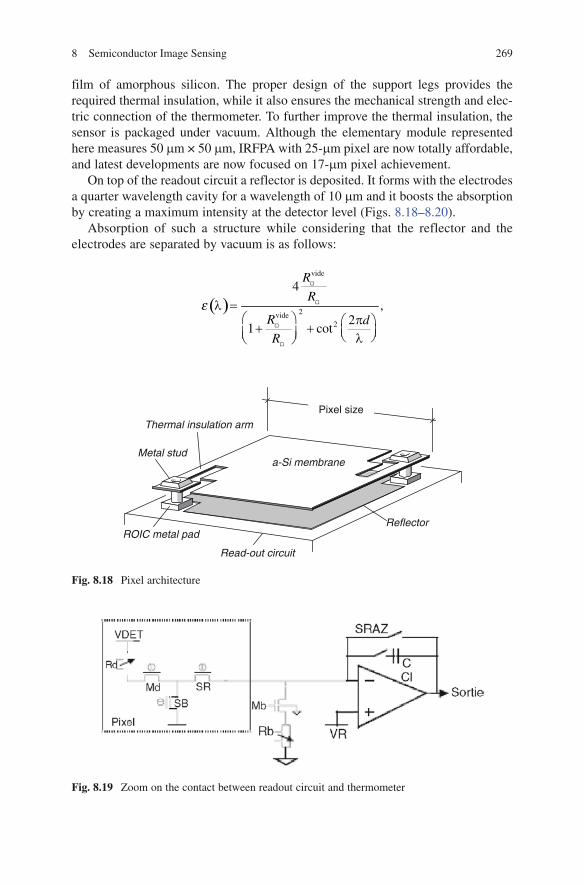
BookID 152004_ChapID 8_Proof# 1 - <Date>
film of amorphous silicon. The proper design of the support legs provides the required thermal insulation, while it also ensures the mechanical strength and elec-tric connection of the thermometer. To further improve the thermal insulation, the sensor is packaged under vacuum. Although the elementary module represented here measures 50 mm × 50 mm, IRFPA with 25-mm pixel are now totally affordable, and latest developments are now focused on 17-mm pixel achievement.
On top of the readout circuit a reflector is deposited. It forms with the electrodes a quarter wavelength cavity for a wavelength of 10 mm and it boosts the absorption by creating a maximum intensity at the detector level (Figs. 8.18–8.20).
Absorption of such a structure while considering that the reflector and the electrodes are separated by vacuum is as follows:
( )
vide
2vide2
4
,2
1 cot
R
R
R d
R
e l =æ ö pæ ö+ + ç ÷ç ÷ è ølè ø
Thermal insulation arm
Reflector
Metal stud
Read-out circuit
ROIC metal pad
a-Si membrane
Pixel size
Fig. 8.18 Pixel architecture
Fig. 8.19 Zoom on the contact between readout circuit and thermometer
where Rp is the resistivity of the electrodes, Rpvide is the resistivity of the vacuum
layer, i.e., 377 W/�, d is the distance between the reflector and the electrodes, and l is the wavelength. The maximum value of e is obtained for a resistivity of the electrode layers equal to the vacuum. In these conditions the device is called adapted.
Absorption modelization of such Fabry Perrot cavity is widely described in the literature.
Focus on MCT
Hg(1−x)CdxTe presents unique properties that make it an ideal candidate for most
of the needs in infrared detection in all the IR spectral bands.First, the bandgap can be tuned by just controlling the xCd/xHg ratio of the alloy,
making possible the entire infrared band to be covered from visible to very long wavelengths (zero bandgap for xCd:0.15) as presented in Fig. 8.21a.
Second, the lattice parameter does not change at the first order from CdTe to HgTe. This allows the use of lattice-matched CdTe substrates. Cd(1−y)Zn
yTe is
more extensively used today for its better quality and because it leads to a perfect lattice matching by adjusting at the second order with yZn composition to the xCd composition. Very high quality epitaxial layers of Hg(1−x)Cd
xTe can be grown today
on very high quality Cd(1−y)ZnyTe oriented substrates with a crystallographic quality
similar to the substrate.
8 Semiconductor Image Sensing 271
BookID 152004_ChapID 8_Proof# 1 - <Date>
The very small lattice parameter variation versus composition makes also possible the fabrication of lattice-matched multilayer epitaxies with only a very small amount of defects and dislocations. Today, very high quality Hg(1−x)Cd
xTe/
Cd(1−y)ZnyTe epitaxies can be grown either by liquid phase epitaxy or by vapor
phase epitaxy (molecular beam epitaxy for example).This semiconductor can be doped n-type (e.g., with indium) and p-type (by mercury
vacancies or arsenic) making possible n on p or p on n junctions to be fabricated.Fundamental parameters such as lifetime are relatively high leading to low
dark current and large quantum efficiency (near 1) photodiodes. Moreover the performances of detectors are only limited by the physics and predictable by validated models in a large domain of temperatures and compositions (see Fig. 8.21b).
This very large flexibility of these alloys makes possible the following:
• The fabrication of a large variety of infrared detectors, in particular, multicolor detectors that need multilayer epitaxies.
• To adjust the composition of the alloys to the useful infrared band to get the ideal composition xCd/operating temperature couple to get the optimum performance for the focal plane array.
Among the other advantages recently pointed out we can mention the following:
• An optimum light collection in backside illumination from the cut-off of the detector to the near UV, including the entire visible spectrum, without any decrease of quantum efficiency.
• A unique specificity in the semiconductor field for MCT avalanche photodiodes that can exhibit very large gain at moderate bias, without any excess of noise [F(K) strictly equal to 1].
All these properties allow this semiconductor to answer all the high performance needs and classes of detectors in infrared bands up to at least 20 mm.
a Dark current of HgCdTe detectors(LETI planar standard technology)
versus cut-off wavelength
FOV=30°FOV=45°FOV=180°
1,00E–07
1,00E–06
1,00E–05
1,00E–04
1,00E–03
1,00E–02
1,00E–01
1,00E+00
1,00E+01
1,00E+02
1,00E+03
2,00 4,00 6,00 8,00 10,00 12,00 14,00 16,00
Cut off wavelength (mm)
Idar
k(A
/cm
²)
30 K 40 K 50 K 60 K70 K 77 K 80 K 90 K110 K 130 K 170 K 200 K250 K 300 K Icc(30°) Icc(45°)Icc(180°)
BLACK BODY at 295 Kη = 50%
b
Si
0
1
2
3
6.55.5 6.0
En
erg
y g
ap
(ele
ctro
n-V
olt
)
lattice parameter (Å)
CdTeCdTe
HgTeHgTe
ZnTe
InAs
GaAs
AlAsGa1-xAlxAsySb1-y
Ga1-xInxAsySb1-y
UV
IR
InSb
GaSb
AlSb1 µm1 µm
12 µm12 µm
Hg 1-x Cd xTeHg 1-x Cd xTe
Fig. 8.21 (a) Lattice parameter of HgCdTe versus composition, (b) Dark current model for n on p photodiodes for cut-off wavelengths from 2 to 16 mm and operating temperature from 30 and 300 K
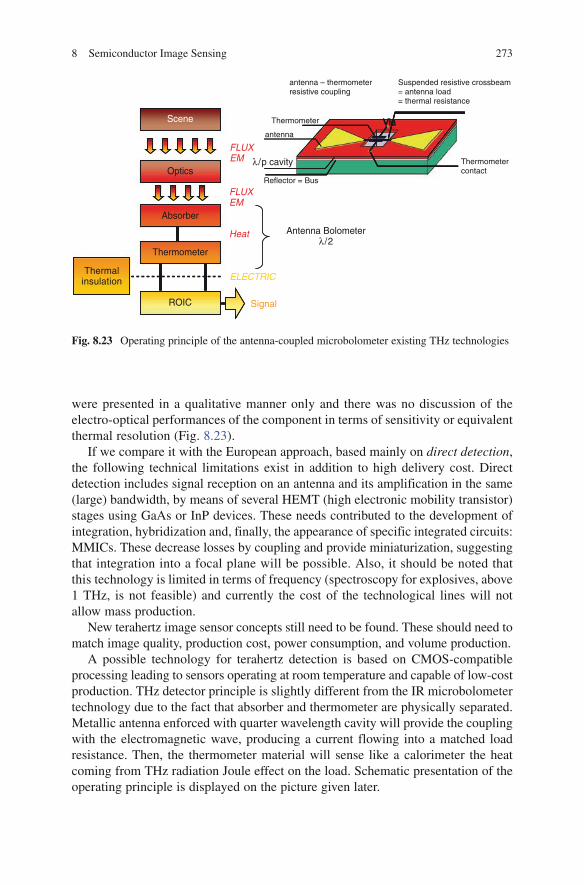
The terahertz (THz) part of the spectrum has recently been investigated. The ability to detect metallic parts under clothes without an ionization source is seen as being the answer to increased screening airport controls after 01/09/11.
Currently, no cost-effective industrial solution exists and thus detectors are still at early development of research and development stage.
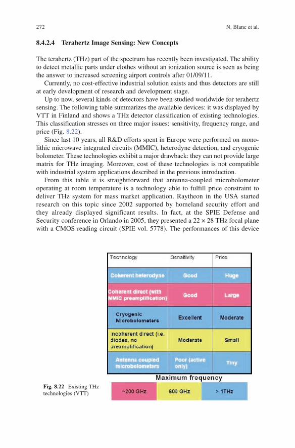
Up to now, several kinds of detectors have been studied worldwide for terahertz sensing. The following table summarizes the available devices: it was displayed by VTT in Finland and shows a THz detector classification of existing technologies. This classification stresses on three major issues: sensitivity, frequency range, and price (Fig. 8.22).
Since last 10 years, all R&D efforts spent in Europe were performed on mono-lithic microwave integrated circuits (MMIC), heterodyne detection, and cryogenic bolometer. These technologies exhibit a major drawback: they can not provide large matrix for THz imaging. Moreover, cost of these technologies is not compatible with industrial system applications described in the previous introduction.
From this table it is straightforward that antenna-coupled microbolometer operating at room temperature is a technology able to fulfill price constraint to deliver THz system for mass market application. Raytheon in the USA started research on this topic since 2002 supported by homeland security effort and they already displayed significant results. In fact, at the SPIE Defense and Security conference in Orlando in 2005, they presented a 22 × 28 THz focal plane with a CMOS reading circuit (SPIE vol. 5778). The performances of this device
Fig. 8.22 Existing THz technologies (VTT)
8 Semiconductor Image Sensing 273
BookID 152004_ChapID 8_Proof# 1 - <Date>
were presented in a qualitative manner only and there was no discussion of the electro-optical performances of the component in terms of sensitivity or equivalent thermal resolution (Fig. 8.23).
If we compare it with the European approach, based mainly on direct detection, the following technical limitations exist in addition to high delivery cost. Direct detection includes signal reception on an antenna and its amplification in the same (large) bandwidth, by means of several HEMT (high electronic mobility transistor) stages using GaAs or InP devices. These needs contributed to the development of integration, hybridization and, finally, the appearance of specific integrated circuits: MMICs. These decrease losses by coupling and provide miniaturization, suggesting that integration into a focal plane will be possible. Also, it should be noted that this technology is limited in terms of frequency (spectroscopy for explosives, above 1 THz, is not feasible) and currently the cost of the technological lines will not allow mass production.
New terahertz image sensor concepts still need to be found. These should need to match image quality, production cost, power consumption, and volume production.
A possible technology for terahertz detection is based on CMOS-compatible processing leading to sensors operating at room temperature and capable of low-cost production. THz detector principle is slightly different from the IR microbolometer technology due to the fact that absorber and thermometer are physically separated. Metallic antenna enforced with quarter wavelength cavity will provide the coupling with the electromagnetic wave, producing a current flowing into a matched load resistance. Then, the thermometer material will sense like a calorimeter the heat coming from THz radiation Joule effect on the load. Schematic presentation of the operating principle is displayed on the picture given later.
8.5 Outlook: The Future of Semiconductor Image Sensing
Thanks to the amazing, relentless progress of semiconductor technology, in particular, the specialized CIS processes that are derived from mainstream CMOS processes; we will soon have more cameras than people on earth. This fact has a rather simple consequence, namely that many more pictures will be acquired than can be looked at by human beings, which is particularly true and worrying in the case of security and surveillance cameras. For this reason, experts agree on the direction electronic imaging will progressively take in the future: Image sensors need to be equipped with an ever-increasing amount of digital processing power, enabling these imagers not only to acquire pictures but also to improve the pictures’ quality with suitable postprocessing and to extract meaningful information about the contents of a scene using powerful object recognition and classification hardware. The goal will be single-chip machine vision systems that “understand” what they see.
Impressed by the demonstration of image sensors with more and more integrated functionality, a prominent researcher in the field proclaimed the imminence of such “seeing chips,” already two decades ago [68]. It is true that for certain tasks, a few examples of image sensors with complete, integrated image processing hardware have been reported, such as single-chip fingerprint recognition and identification systems. Other types of smart image sensors have been demonstrated that are capable of carrying out a few important, but still only rather basic functions for the vision process on a single chip. The more research results are reported, however, the more obvious it becomes that “vision is difficult,” as suspected in [68]. It is clear now that early expectations of monolithically integrated single-chip vision systems were too high. While it is possible today to cointegrate an image sensor and all the necessary processing circuitry on a single chip for the solution of a given, not too complex, machine vision problem, such an accomplishment is far removed, though, from the original idea of a seeing chip, capable of visually perceiving important aspects of an imaged scene.
The main obstacle is not a technological one: today, a lot of digital processing power and memory can be packed onto a single chip. The problem is rather our still very limited understanding of the natural vision process and how to translate it into reliably working algorithms, for which dedicated circuitry can be fabricated on a “smart” image sensor. Despite almost 50 years of research in machine vision, the man-made, robust machine vision system performing as well as natural vision systems, such as the visual sense of insects, are still elusive. Recent research is increasingly taking clues from the successful natural vision systems, where evidence can be found that all kinds of cognitive functions in humans are implemented with the same basic functionality and system architecture, the so-called Mountcastle observation [69]. This is an exciting prospect, of course, that may not only lead the way to “seeing chips” but also to “hearing microphones” and – more generally – to “aware sensors.” In any case, all these developments clearly require more insight and for its implementation more microelectronic functionality on each chip – more Moore, and more than Moore!
8 Semiconductor Image Sensing 275
BookID 152004_ChapID 8_Proof# 1 - <Date>
References
1. S.M. Sze, “Semiconductor Devices – Physics and Technology,” 2nd edition, Wiley, New York, 1992.
2. T. Spirig, “Smart CCD/CMOS Based Image Sensors with Programmable, Real-time, Temporal and Spatial Convolution Capabilities for Applications in Machine Vision and Optical Metrology,” Thesis, ETH Zurich, No. 11993, 1997, Chapter 3.
3. P.J.W. Noble, “Self-Scanned Silicon Image Detector Array,” IEEE Trans. Electron Devices, Vol. 15, pp. 202–209, 1968.
4. E.R. Fossum, “Active Pixel Sensors: Are CCD’s Dinosaurs?,” Proc. SPIE, Vol. 1900, pp. 2–14, 1993.
5. H.S. Wong, “Technology and Device Scaling Considerations for CMOS Imagers,” IEEE Trans. Electron. Devices, Vol. 43, pp. 2131–2142, 1996.
6. G. Agranov et al., “Super Small, Sub 2mm Pixels for Novel CMOS Image Sensors,” Proc. 2007 International Image Sensor Workshop, pp. 307–310, 2007.
7. P. Seitz, “Solid-State Image Sensing,” in Computer Vision and Applications – A Guide for Students and Practitioners, B. Jähne, and H. Haussecker (Eds.), pp. 111–152, Academic, San Diego, 2000.
8. Y. Lim et al., “Stratified Photodiode – A New Concept for Small Size High Performance CMOS Image Sensor Pixels,” Proc. 2007 International Image Sensor Workshop, pp. 311–315, 2007.
9. N. Wyrsch et al., “Vertical Integration of Hydrogenated Amorphous Silicon Devices on CMOS Circuits,” Mater. Res. Soc. Symp. Proc., Vol. 869, pp. D1.1.1–D1.1.12, 2005.
10. P. Seitz, “Smart Pixel Arrays,” in Encyclopaedia of Modern Optics, B. Guenther and D. Steel (Eds.), Elsevier, Oxford, 2005.
11. A. Krimsky, N. Khaliullin and H. Rhodes, “A 2 e− Noise 1.3 Megapixel CMOS Sensor,” Proc. 2003 IEEE Workshop on Charge-Coupled Devices and Advanced Image Sensors, May 15–17, 2003.
12. C. Koch, “Seeing Chips: Analog VLSI Circuits for Computer Vision,” Neural Comput., Vol. 1, pp. 184–200, 1989.
13. J. Hawkins and S. Blakeslee, On Intelligence, Henry Holt, New York, 2004. 14. S. Tanner, S.C. Lauxtermann, M. Waeny, M. Willemin, N. Blanc, J. Grupp, R. Dinger, E.
Doering, M. Ansorge, P. Seitz and F. Pellandini, “Low-Power Digital Image Sensor for Still-Picture Image Acquisition,” Proc. SPIE Int. Soc. Opt. Eng., Vol. 4306, p. 358, 2001.
15. K.B. Cho, A Krymski and E.R. Fossum, “A Micropower Self-Clocked Camera-on-a-Chip,” IEEE Workshop on Charge-Coupled Devices and Advanced Image Sensors, Cal-Neva Resort, NV, USA, pp. 12–13, June 7–9, 2001; K.B. Cho et al., “A 1.2V Micropower CMOS Active Pixel Image Sensor for Portable Applications,” ISSCC Digest of Tech. Papers, pp. 114–115, Feb. 2000.
17. T.G. Etoh et al., “An Image Sensor Which Captures 100 Consecutive Frames at 1000000 fps,” IEEE Trans. Electron Devices, Vol. 50, No. 1, pp. 144–151, Jan. 2003.
18. S. Kleinfelder et al., “A 10kframe/s 0.18 um CMOS Digital Pixel Sensor with Pixel-Level Memory,” Proc. IEEE ISSCC-01 Conf., Vol. XLIV, pp. 88–89, Feb. 2001.
19. S. Lauxtermann, et al., “A High Speed CMOS Imager Acquiring 5000 Frames/Sec,” Dig. IEDM ‘99 Conf., pp. 875–878, Dec. 1999.
20. Z. Zhou, B. Pain and E.R. Fossum, “CMOS Active Pixel Sensor with On-Chip Successive Approximation Analog-to-Digital Converter,” IEEE Trans. Electron Devices, Vol. 44, No. 10, pp. 1759–1763, Oct. 1997.
21. A. Krymski et al., “A High Speed, 500 fps, 1024 × 1024 CMOS Active Pixel Sensor,” IEEE VLSI Circuits Conf. Dig., pp. 137–138, June 1999.
22. Micron Technology Inc., “MT9M413 1.3 Mpix CMOS Active Pixel Digital Sensor,” Datasheet, Ver. 3.0, Jan. 2004.
23. O. Yadid-Pecht et al., “A Random Access Photodiode Array for Intelligent Image Capture,” IEEE Trans. Electron Devices, Vol. 38, No. 8, pp. 1772–1780, Aug. 1991.
24. A. Krymski and N. Tu, “A 9VLux-s 5000fps 512 × 512 CMOS Sensor,” IEEE Trans. Electron Devices, Vol. 50, No. 1, pp. 136–143, Jan. 2003.
25. S. Kleinfeld, “High-Speed, High-Sensitivity, Low-Noise CMOS Scientific Image Sensors,” Proc. SPIE, Vol. 5274, pp. 194–205, March 2004.
26. T. Inoue et al., “A CMOS Active Pixel Image Sensor with In-Pixel CDS for High-Speed Cameras,” Proc. SPIE, Vol. 5580, pp. 293–300, 2005.
27. R. Aerts et al., “1.4Gpix/s, 2.9Mpix CMOS Image Sensor for Readout of Holographic Data Memory,” Proc. IEEE International Image Sensor Workshop, Ses. 06, pp. 74–77, June 2007.
28. M. Furuta et al., “A High-Speed, High-Sensitivity Digital CMOS Image Sensor with a Global Shutter and 12-Bit Column-Parallel Cyclic A/D Converters,” IEEE JSSC, Vol. 42, No. 4, pp. 766–774, April 2007.
29. I. Takayagani et al., “A 600 × 600 Pixel, 500fps CMOS Image Sensor with 4.4um Pinned Photodiode 5-Transistor Global Shutter Pixel,” Proc. IEEE International Image Sensor Workshop, Ses. 17, pp. 287–290, June 2007.
30. Y. Nitta et al., “High-Speed Digital Double Sampling with Analog CDS on Column Parallel ADC Architecture for Low-Noise APS,” Proc. IEEE ISSCC’06, pp. 2024–2031, 6–9 Feb. 2006.
31. A. Krymski, “A High Speed 4 Megapixel Digital CMOS,” Proc. IEEE International Image Sensor Workshop, Ses. 06, pp. 78–81, June 2007.
32. T. Cools et al., “An SXGA CMOS Image Sensor with 8Gbps LVDS Serial Link,” Proc. IEEE International Image Sensor Workshop, Ses. 17, pp. 283–286, June 2007.
33. A. Krymski and K. Tajima, “CMOS Image Sensor with Integrated 4Gbs Camera Link Transmitter,” Proc. IEEE ISSCC’06, pp. 2040–2049, 6–9 Feb. 2006.
34. S. Kawahito, “CMOS Imaging Devices for New Markets of Vision Systems,” IEICE Trans. Electron., Vol. E90-C, No. 10, pp. 1858–1868, Oct. 2007.
35. R. Johansson et al., “A Multi-Resolution 100 GOPS 4 Gpixels/s Programmable CMOS Image Sensor for Machine Vision,” Proc. IEEE Workshop on CCD & AIS, May 2003.
36. T. Oggier et al., “An All-Solid-State Optical Range Camera for 3D Real-Time Imaging with Sub-Centimeter Depth Resolution (Swissranger),” Proc. SPIE 5249, pp. 534–545, 2003.
37. R. Lange and P. Seitz, “A Solid State Time-of-Flight Range Camera,” IEEE J. Quant. Electron., Vol. 37, p. 390, 2001.
38. R. Kaufmann et al., “A Time-of-Flight Line Sensor – Development and Application,” Proc. SPIE 5459, pp. 192–199, 2004.
39. http://www.mesa-imaging.ch; http://www.canesta.com; http://www.pmdtec.com.40. http://www.mesa-imaging.ch/prodviews.php.41. I.A.H. Izhal, T. Ushinaga, T. Sawada, M. Homma, Y. Maeda and S. Kawahito, “A CMOS
Time-of-Flight Range Image Sensor with Gates on Field Oxide Structure,” Proc. Fourth IEEE Int. Conf. Sensors, pp. 141–144, Nov. 2005.
42. B. Braun, Electromedica, Vol. 70, p. 1, 2002. 43. J.P. Moy, Thin Solid Films, Vol. 337, p. 213, 1999. 44. A. Oppelt (Ed.), Imaging Systems for Medical Diagnosis, Publicis, Erlangen, 2005. 45. L.D. Hubbard, R.J. Brothers, W.N. King, L.X. Clegg, R. Klein, L.S. Cooper, A.R. Sharrett,
M.D. Davis and J. Cai, Ophthalmology, Vol. 106, p. 2269, 1999. 46. M. Hoheisel and L. Bätz, Thin Solid Films, Vol. 383, p. 132, 2001. 47. M. Hoheisel, J. Giersch and P. Bernhardt, Nucl. Instr. Meth., Vol. 5ANS-531/1–2, p. 75, 2004. 48. M. Hoheisel, L. Bätz, T. Mertelmeier, J. Giersch and A. Korn, Modulation Transfer Function
of a Selenium-Based Digital Mammography System, in IEEE Proceedings of the Nuclear Science Symposium, Medical Imaging Conference, pp. 3589–3593, 2004.
49. S. Thunberg, H. Sklebitz, B. Ekdahl, L. Bätz, A. Lundin, H. Möller, F. Fleischmann, G. Kreider and T. Weidner, Proc. of SPIE, Vol. 3659, p. 150, 1999.
8 Semiconductor Image Sensing 277
BookID 152004_ChapID 8_Proof# 1 - <Date>
50. R.A. Street, W.S. Wong, S. Ready, R. Lujan, A.C. Arias, M.L. Chabinyc, A. Salleo, R. Apte and L.E. Antonuk, Proc. SPIE Med. Imaging Conf., Vol. 5745, p. 7, 2005.
51. G.B. Avinash, K.N. Jabri, R. Uppaluri, A. Rader, F. Fischbach, J. Ricke and U. Teichgräber, Proc. SPIE, Vol. 4684, p. 1048, 2002.
52. J.M. Lewin, P.K. Isaacs, V. Vance and F.J. Larke, Radiology, Vol. 229, p. 261, 2003. 53. L. Tlustos, R. Ballabriga, M. Campbell, E. Heijne, K. Kincade, X. Llopart and P. Stejskal,
“Imaging Properties of the Medipix-2 System Exploiting Single and Dual Energy Thresholds,” Proceedings of the IEEE Medical Imaging Conference, Rome, N43–3, 2004
54. M. Hoheisel, R. Lawaczeck, H. Pietsch and V. Arkadiev, Proc. SPIE, Vol. 5745, p. 1087, 2005. 55. E. Pisano et al., Radiology, Vol. 214, p. 895, 2000. 56. S.W. Wilkins, T.E. Gureyev, D. Gao, A. Pogany and A.W. Stevenson, Nature, Vol. 384,
p. 335, 1996. 57. G. Destefanis, Electrical Doping of HgCdTe by Ion Implantation and Heat Treatment, Third
International Conference on II–VI Compounds, Monterey, USA, July 1987; J. Cryst. Growth, Vol. 86, pp. 700–727, 1988.
58. G. Destefanis, HgCdTe Infrared Diodes Arrays, Nato Workshop on Narrow Bandgap Semiconductors, Oslo, Norway, 1991; Semicond. Sci. Technol., Vol. 6, pp. 88–92, 1991.
59. G. Destefanis and J.P. Chamonal, Large Improvement in HgCdTe Photovoltaic Detector Performance at LETI, The US Workshop on the Physics and Chemistry of II–VI Materials, Danvers, USA, October 1992; J. Electron. Mater., Vol. 22, No. 8, pp. 1027–1032, 1993.
60. G. Destefanis, P. Audebert, E. Mottin and P. Rambaud, High Performance LWIR 256 × 256 HgCdTe Focal Plane Array Operating at 88 K, International SPIE Conference, Orlando (USA), April 1997; Proc. SPIE, Vol. 3061, pp. 111–116, 1997
61. P. Tribolet, P. Bensussan and G. Destefanis, SOFRADIR Approach for 2/5 and 3rd Generations of IR Detectors, The Fifth International Military Sensing Symposium: 2002DTB04, Washington, USA, Dec. 2002, Org. OTAN.
62. G. Destefanis, A. Bain, J. Baylet, P. Castelein, E. De Borniol, O. Gravrand, F. Marion, A. Million, Ph. Rambaud, F. Rothan, J.L. Martin and P. Martin, Recent Developments of High Complexity HgCdTe Focal Plane Arrays at LETI Infrared Laboratory, The 2002 Workshop on the Physics of II–VI material, Nov. 2002, San Diego, USA; J. Electron. Mater., Vol. 32, No. 7, pp. 592–601, 2003.
63. F.P. Pistone, S. Dugalleix, P. Tribolet and G. Destefanis, Progress in MCT Large Staring Arrays, International SPIE Meeting Infrared Detectors and Focal Plane Arrays VIII, San Diego, USA, Aug. 2006; SPIE Proc., Vol. 6295–21.
64. P. Tribolet and G. Destefanis, HgCdTe Large Staring Arrays at Sofradir, The 19th International Technology Conference on Photoelectronis and Nigh Vision Devices, 2006 (to be published in SPIE Proceedings).
65. P. Tribolet, S. Blondel, P. Costa, A. Combette, L. Vial, G. Destefanis, Ph. Ballet, J.P. Zanatta, O. Gravrand, C. Largeron, J.P. Chamonal and A. Million, MWIR Focal Plane Arrays Made with HgCdTe Grown by MBE on Germanium Substrates, International SPIE Meeting Infrared Technology and Application XXXII, Orlando, USA, April 2006; SPIE Proc., Vol. 6206–82.
66. J.P. Zanatta, G. Badano, Ph. Ballet, J. Baylet, O. Gravrand, J. Rothman, P. Castelein, J.P. Chamonal, A. Million and G. Destefanis, MBE HgCdTe Growth on Ge for the 3rd Generation of Infrared Detectors, The 2005 US Workshop on the Physics and Chemistry of II–VI Materials, Boston, USA, Sept. 2005; J. Electron. Mater., Vol. 35, p. 6, 2006.
67. J. Baylet, Ph. Ballet, P. Castelein, F. Rothan, M. Fendler, E. Laffosse, J.P. Zanatta, J.P. Chamonal, A. Million and G. Destefanis, TV/4 Dual Band HgCdTe Infrared Focal Plane Arrays with a Pitch of 25mm and Spatial Coherence, The 2005 US Workshop on the Physics and Chemistry of II–VI Materials, Boston, USA, Sept. 2005; J. Electron. Mater., Vol. 35, p. 6, 2006.
68. P. Chorier, P. Tribolet and G. Destefanis, From Visible to Infrared: A New Approach, International SPIE Meeting Infrared Technology and Application XXXII, Orlando, USA, April 2006; SPIE Proc., Vol. 6206–01.
278 N. Blanc et al.
BookID 152004_ChapID 8_Proof# 1 - <Date>
69. O. Gravrand, E. Deborniol, G. Destefanis, A. Manissadjian, P. Tribolet, C. Pautet, P. Chorier, From LWIR to VLWIR FPAs Made with HgCdTe at Defir, International SPIE Meeting Sensors, Systems and Next generation Satellites XII, Stockholm, Sweden, Sept. 2006; SPIE Proc., Vol. 6361–42.
70. O. Gravrand, E. Deborniol and G. Destefanis, From LWIR to VLWIR FPAs Made with HgCdTe n+n/p Ion Implantation Technology, The 2006 US Workshop on the Physics and Chemistry of II-VI Materials, Newport, USA, Oct. 2006; J. Electron. Mater., in press
71. E. Deborniol, G. Destefanis, A. Manissadjian and P. Tribolet, Characterization of High Performance Long Wave and Very Long Wave HgCdTe Staring Arrays, International SPIE Meeting: Remote Sensing, Bruges, Belgium, Sept. 2005; SPIE Proc., Vol. 5978–44.
72. A. Manissadjian, P. Tribolet, G. Destefanis and E. Deborniol; Long Wave HgCdTe Staring Arrays at Sofradir: From 9mm to 13+mm Cut-Off for High Performance Applications, International SPIE Meeting Infrared Technology and Application XXXI, Orlando, USA, April 2005; SPIE Proc., Vol. 5783.
73. G. Destefanis, J. Baylet, P. Ballet, F. Rothan, O. Gravrand, J. Rothman, J.P. Chamonal and A. Million, Status of HgCdTe Bicolour and Dual Band Infrared Focal Plane Arrays at LETI, The 2006 US Workshop on the Physics and Chemistry of II–VI Materials, Newport, USA, Oct. 2006; J. Electron. Mater., 2007.
74. G. Destefanis, Ph. Ballet, J. Baylet, P. Castelein, O. Gravrand, J. Rothman, F. Rothan, G. Perrais, J. Chamonal, A. Million, P. Tribolet, B. Terrier, E. Sanson, P. Costa and L. Vial, Bi-Color and Dual Band Infrared Focal Plane Arrays at Defir, International SPIE Meeting Infrared Technology and Application XXXII, Orlando, USA, April 2006; SPIE Proc., Vol. 6206–27.
75. P. Ballet, P. Castelein, J. Baylet, E. Laffosse, M. Fendler, F. Pottier, S. Gout, C. Vergnaud, S. Ballerand, O. Gravrand, J.C. Desplanches, S. Martin, J.P. Zanatta, J.P. Chamonal, A. Million and G. Destefanis, Demonstration of a 25mm Pitch Dual Band HgCdTe Infrared Focal Plane Array with Spatial Coherence, International SPIE Meeting Optics and Optoelectronics, Bruges, Belgium, Sept. 2005; SPIE Proc., Vol. 5978–44.
76. P. Tribolet and G. Destefanis, Third Generation and Multicolour IRFPA Developments: A Unique Approach Based on Defir, International SPIE Meeting Infrared Technology and Application XXXI, Orlando, USA, April 2005; SPIE Proc., Vol. 5783.
77. F. Ma et al., Phys. Rev. Lett., Vol. 95, p. 176604, 2005. 78. R. Alabedra et al., IEEE Trans. Electron Devices, Vol. ED-32, p. 1302, 1985; G. Levêque
et al., Semicond. Sci. Technol., Vol. 8, p. 1317, 1993. 79. J.D. Beck, C.-F.Wan, M.A. Kinch, J.E. Robinson, Proc. SPIE, Vol. 4454, p. 188, 2001; J.D.
Beck, C.-F. Wan, M.A. Kinch, J.E. Robinson, P. Mitra, R. Scrithfield, F. Ma and J. Campbell, J. Electron. Mater., Vol. 35, p. 1166, 2006.
80. G. Perrais, O. Gravrand, J. Baylet, G. Destefanis and J. Rothman, Gain and Dark Current Characteristics of Planar HgCdTe Avalanche Photodiodes, The 2006 US Workshop on the Physics and Chemistry of II VI Materials, Newport, USA, Oct. 2006; J. Electron. Mater., 2007.
81. G. Perrais, O. Gravrand, J. Baylet, G. Destefanis and J. Rothman, Gain and Dark Current Characteristics of Planar HgCdTe Avalanche Photodiodes, The 2006 US Workshop on the Physics and Chemistry of II–VI materials, Newport, USA, Oct. 2006; J. Electron. Mater. 2007.
82. G. Perrais, J. Rothman, G. Destefanis, J.P. Baylet, P. Castelein, J. Chamonal, P. Tribolet, Demonstration of Multifunction Bicolour Avalanche Gain in HgCdTe FPA, International SPIE Meeting Electro Optical and Infrared Systems: Technology and Applications III, Stockholm, Sweden, Sept. 2006; SPIE Proc, Vol. 6395–16.