20
Terasic THDB-HTG THDB THDB THDB THDB-HTG HTG HTG HTG Terasic HSTC to GPIO Daughter Board User Manual Document Version 1.0.2 DEC. 23, 2008 by Terasic

Terasic THDB-HTG
THDBTHDBTHDBTHDB----HTGHTGHTGHTG Terasic HSTC to GPIO Daughter Board
User Manual
Document Version 1.0.2 DEC. 23, 2008 by Terasic

IntroductionIntroductionIntroductionIntroduction
ii
Page Index
INTRODUCTION ..............................................................................................................................................................................1
1-1 FEATURES................................................................................................................................................................................... 1
1-2 GETTING HELP ........................................................................................................................................................................... 1
ARCHITECTURE .............................................................................................................................................................................2
1-3 LAYOUT AND COMPONETS.......................................................................................................................................................... 2
1-4 BLOCK DIAGRAM ........................................................................................................................................................................ 4
BOARD COMPONENTS .................................................................................................................................................................5
1-5 HSTC/HSMC EXPANSION CONNECTOR................................................................................................................................... 5
1-6 EXPANSION PROTOTYPE CONNECTORS .................................................................................................................................... 7
1-7 CYCLONE III STARTER BOARD HSMC CONNECTOR............................................................................................................... 12
1-8 PROTOTYPING AREA ................................................................................................................................................................ 12
1-9 JTAG SWITCH .......................................................................................................................................................................... 13
1-10 POWER ON CONTROL PIN..................................................................................................................................................... 14
1-11 I2C SERIAL EEPROM ........................................................................................................................................................... 14
1-12 POWER SUPPLY ..................................................................................................................................................................... 15
DEMONSTRATION ........................................................................................................................................................................16
1-13 CONNECTING THDB-HTG BOARD TO A CYCLONE III STARTER BOARD .............................................................................. 16
1-14 CONNECTING THDB-HTG BOARD TO ALTERA DE3 BOARD ................................................................................................ 17
APPENDIX ......................................................................................................................................................................................18
1-15 REVISION HISTORY ................................................................................................................................................................ 18
1-16 ALWAYS VISIT THDB-HTG WEBPAGE FOR NEW MAIN BOARD ............................................................................................ 18

Introduction
1
1
Introduction The THDB-HTG board is designed to convert a High-Speed Terasic connector (HSTC) or a High-Speed
Mezzanine connector (HSMC) I/Os to three 40-pin expansion prototype connectors, which are compatible
with Altera DE2/DE1 expansion headers. Users can connect up to three Altera DE2/DE1 boards (or
associated daughter cards) onto a HSTC/HSMC-interfaced host board via a THDB-HTG board.
1-1Features
Figure 1.1 shows the photo of a THDB-HTG board. The important functions of the THDB-HTG are listed
below:
• Convert HSTC/HSMC-interfaced I/O to standard 40-pin expansion connectors.
• Allow users to connect Altera DE2/DE1 boards to a HSTC/HSMC-interfaced host board.
• Provide test points for signal measurement.
Figure 1.1. The picture of a THDB-HTG board
1-2Getting Help Here are some places to get help if you encounter any problem:
� Email to [email protected]
� Taiwan & China: +886-3-550-8800
� Korea : +82-2-512-7661
� English Support Line: +1-408-512-12336

Architecture
2
2
Architecture This chapter describes the architecture of the THDB-HTG board, including block diagram and components.
1-3Layout and Componets
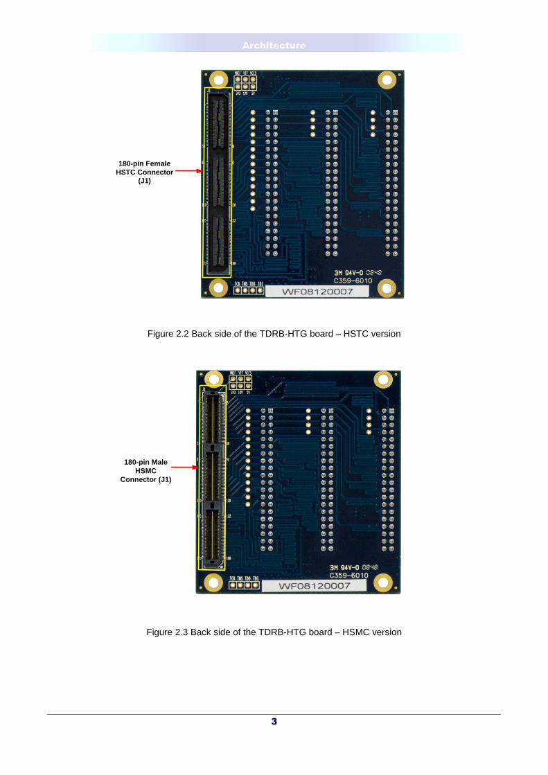
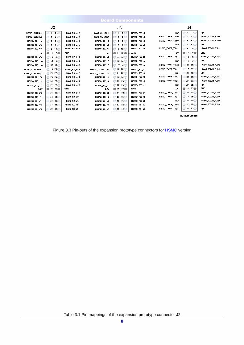
Figure 2.1, Figure 2.2, and Figure 2.3 depict the layout of the board and indicate the locations of the connectors
and key components.
Expansion Prototype
Connector (J2)
Expansion Prototype
Connector (J3)
Expansion Prototype
Connector (J4)
Prototype Area
Prototype Area
I2C SerialEEPROM(U1)
JTAGSwitch (SW1)
Figure 2.1 Top view of the TDRB-HTG board
Architecture
3
180-pin FemaleHSTC Connector
(J1)
Figure 2.2 Back side of the TDRB-HTG board – HSTC version
180-pin MaleHSMC
Connector (J1)
Figure 2.3 Back side of the TDRB-HTG board – HSMC version

Architecture
4
The following components are provided on the THDB-HTG board :
• HSTC/HSMC expansion connector (J1)
• Expansion prototype connectors (J2,J3,J4)
• I2C serial EEPROM (U1)
1-4Block Diagram
Figure 2.4 shows the block diagram of the THDB-HTG board.
To HSTC/HSMCInterface
Host Board
HSTC/HSMCConnector
40-Pin ExpansionPrototype Connector 1
J2
40-Pin ExpansionPrototype Connector 3
J4
Prototype Area
40-Pin ExpansionPrototype Connector 2
J3
I2C Serial EEPROMU1
36 I/Os
36 I/Os
36 I/Os
22 I/Os
I2C Interface
J1
Figure 2.4. The block diagram of the THDB-HTG board

Board Components
5
3
Board Components This section will describe the information of components, connector interfaces, and pin
mappings on the THDB-HTG board in details.
1-5HSTC/HSMC Expansion Connector
This section describes the HSTC/HSMC connector on the THDB-HTG board
There are two options of high speed connector on the THDB-HTG board. One is a 180-pin female HSTC
connector for HSTC-interfaced host board such as Altera DE3 board and Terasic PCI board. The other one is
a 180-pin male connector for Altera HSMC-interfaced host board. All other interfaces on the THDB-HTG board
are connected to the HSTC/HSMC connector. Figure 3.1 shows the pin-outs of the HSTC and HSMC
connector.

Board Components
6
22
44 HSTCA_CLKIN_n0
HSTCA_CLKIN_p0
HSTCA_RX_n0HSTCA_RX_p0
HSTCA_RX_n1HSTCA_RX_p1
HSTCA_RX_n2HSTCA_RX_p2
HSTCA_RX_n3HSTCA_RX_p3
HSTCA_RX_n4HSTCA_RX_p4
HSTCA_RX_n5HSTCA_RX_p5
HSTCA_RX_n6HSTCA_RX_p6
HSTCA_RX_n7HSTCA_RX_p7
HSTCA_RX_n8HSTCA_RX_p8
66
88
1010
1212
1414
1616
1818
2020
2222
2424
2626
2828
3030
3232
3434
3636
3838
4040
4242
4444
4646
4848
5050
5252
5454
5656
5858
6060
HSTCA_CLKIN_n164
64HSTCA_CLKIN_p1
6666
HSTCA_RX_n970
70HSTCA_RX_p9
7272
6262
6868
HSTCA_RX_n1076
76HSTCA_RX_p10
7878
7474
HSTCA_RX_n1182
82HSTCA_RX_p11
8484
8080
HSTCA_RX_n1288
88HSTCA_RX_p12
9090
8686
HSTCA_RX_n1394
94HSTCA_RX_p13
9696
9292
HSTCA_RX_n14100
100HSTCA_RX_p14
102102
9898
HSTCA_RX_n15106
106HSTCA_RX_p15
108108
104104
HSTCA_RX_n16112
112HSTCA_RX_p16
114114
110110
HSTCA_RX_n17118
118HSTCA_RX_p17
120120
122122
HSTCA_CLKIN_2VCC50
BA_VTT
124124
124 HSTCA_TDI
HSTCA_TMS
126126
128128
130130
HSTCA_SCL132
132HSTCA_RX_n18
134134
HSTCA_RX_p18136
136HSTCA_RX_n19
138138
HSTCA_RX_p19140
140HSTCA_RX_n20
142142
HSTCA_RX_p20144
144HSTCA_RX_n21
146146
HSTCA_RX_p21148
148HSTCA_RX_n22
150150
HSTCA_RX_p22152
152HSTCA_RX_n23
154154
HSTCA_RX_p23156
156HSTCA_RX_n24
158158
HSTCA_RX_p24160
160HSTCA_RX_n25
162162
HSTCA_RX_p25164
164HSTCA_RX_n26
166166
HSTCA_RX_p26168
168HSTCA_RX_n27
170170
HSTCA_RX_p27172
172HSTCA_RX_n28
174174
HSTCA_RX_p28176
176HSTCA_RX_n29
178178
HSTCA_RX_p29180
180
116116
13579
11131517192123252739313335373941434547495153555759
6365
6971
61
67
7577
73
8183
79
8789
85
9395
91
99101
97
105107
103
111113
109
117119
121123125127129131133135137139141143145147149151153155157159161163165167169171173175177179
115
13579
11131517192123252739313335373941434547495153555759
6365
6971
61
67
7577
73
8183
79
8789
85
9395
91
99101
97
105107
103
111113
109
117119
121123125127129131133135137139141143145147149151153155157159161163165167169171173175177179
115
HSTCA_CLKOUT_n0
VCC33 12V
J1
HSTCA_CLKOUT_p0
HSTCA_TX_n0HSTCA_TX_p0
HSTCA_TX_n1HSTCA_TX_p1
HSTCA_TX_n2HSTCA_TX_p2
HSTCA_TX_n3HSTCA_TX_p3
HSTCA_TX_n4HSTCA_TX_p4
HSTCA_TX_n5HSTCA_TX_p5
HSTCA_TX_n6HSTCA_TX_p6
HSTCA_TX_n7HSTCA_TX_p7
HSTCA_TX_n8HSTCA_TX_p8
HSTCA_CLKOUT_n1HSTCA_CLKOUT_p1
HSTCA_TX_n9HSTCA_TX_p9
HSTCA_TX_n10HSTCA_TX_p10
HSTCA_TX_n11HSTCA_TX_p11
HSTCA_TX_n12HSTCA_TX_p12
HSTCA_TX_n13HSTCA_TX_p13
HSTCA_TX_n14HSTCA_TX_p14
HSTCA_TX_n15HSTCA_TX_p15
HSTCA_TX_n16HSTCA_TX_p16
HSTCA_TX_n17HSTCA_TX_p17
HSTCA_CLKOUT_2POWER ON
BA_VREF
HSTCA_TDO
HSTCA_TCKHSTCA_SDAHSTCA_TX_n18HSTCA_TX_p18HSTCA_TX_n19HSTCA_TX_p19HSTCA_TX_n20HSTCA_TX_p20HSTCA_TX_n21HSTCA_TX_p21HSTCA_TX_n22HSTCA_TX_p22HSTCA_TX_n23HSTCA_TX_p23HSTCA_TX_n24HSTCA_TX_p24HSTCA_TX_n25HSTCA_TX_p25HSTCA_TX_n26HSTCA_TX_p26HSTCA_TX_n27HSTCA_TX_p27HSTCA_TX_n28HSTCA_TX_p28HSTCA_TX_n29HSTCA_TX_p29
HSMC_CLKINn2HSMC_CLKINp2
HSMC_RX_n16HSMC_RX_p16
HSMC_RX_n15HSMC_RX_p15
HSMC_RX_n14HSMC_RX_p14
HSMC_RX_n13HSMC_RX_p13
HSMC_RX_n12HSMC_RX_p12
HSMC_RX_n11HSMC_RX_p11
HSMC_RX_n10HSMC_RX_p10
HSMC_RX_n9HSMC_RX_p9
HSMC_RX_n8HSMC_RX_p8
HSMC_CLKINn1HSMC_CLKINp1
HSMC_RX_n7HSMC_RX_p7
HSMC_RX_n6HSMC_RX_p6
HSMC_RX_n5HSMC_RX_p5
HSMC_RX_n4HSMC_RX_p4
HSMC_RX_n3HSMC_RX_p3
HSMC_RX_n2HSMC_RX_p2
HSMC_RX_n1HSMC_RX_p1
HSMC_RX_n0HSMC_RX_p0
HSMC_D3HSMC_D1
HSMC_CLKIN0HSMC_TDI
HSMC_TMSHSMC_SCLNDHSMC_TXVR_RXn0HSMC_TXVR_RXP0NDHSMC_TXVR_RXn1HSMC_TXVR_RXp1NDHSMC_TXVR_RXn2HSMC_TXVR_RXp2NDHSMC_TXVR_RXn3HSMC_TXVR_RXp3NDHSMC_TXVR_RXn4HSMC_TXVR_RXp4NDHSMC_TXVR_RXn5HSMC_TXVR_RXp5NDHSMC_TXVR_RXn6HSMC_TXVR_RXp6NDHSMC_TXVR_RXn7HSMC_TXVR_RXp7
2468
1012141618202224262830323436384042444648505254565860
6466
7072
62
68
7678
74
8284
80
8890
86
9496
92
100102
98
106108
104
112114
110
118120
122124126128130132134136138140142144146148150152154156158160162164166168170172174176178180
116
24681012141618202224262830323436384042444648505254565860
6466
7072
62
68
7678
74
8284
80
8890
86
9496
92
100102
98
106108
104
112114
110
118120
122124126128130132134136138140142144146148150152154156158160162164166168170172174176178180
116
13579
11131517182123252729313335373941434547495153555759
6365
6971
61
67
7577
73
8183
79
8789
85
9395
91
99101
97
105107
103
111113
109
117119
121123125127129131133135137139141143145147149151153155157159161163165167169171173175177179
115
1357911131517192123252729313335373941434547495153555759
6365
6971
61
67
7577
73
8183
79
8789
85
9395
91
99101
97
105107
103
111113
109
117119
121123125127129131133135137139141143145147149151153155157159161163165167169171173175177179
115
VCC33 12V
J1
HSMC_CLKOUTn2HSMC_CLKOUTp2
HSMC_TX_n16HSMC_TX_p16
HSMC_TX_n15HSMC_TX_p15
HSMC_TX_n14HSMC_TX_p14
HSMC_TX_n13HSMC_TX_p13
HSMC_TX_n12HSMC_TX_p12
HSMC_TX_n11HSMC_TX_p11
HSMC_TX_n10HSMC_TX_p10
HSMC_TX_n9HSMC_TX_p9
HSMC_TX_n8HSMC_TX_p8
HSMC_CLKOUTn1HSMC_CLKOUTp1
HSMC_TX_n7HSMC_TX_p7
HSMC_TX_n6HSMC_TX_p6
HSMC_TX_n5HSMC_TX_p5
HSMC_TX_n4HSMC_TX_p4
HSMC_TX_n3HSMC_TX_p3
HSMC_TX_n2HSMC_TX_p2
HSMC_TX_n1HSMC_TX_p1
HSMC_TX_n0HSMC_TX_p0
HSMC_D2HSMC_D0
HSMC_CLKOUT0ND
HSMC_TDO
HSMC_TCKHSMC_SDANDHSMC_TXVR_TXn0HSMC_TXVR_TXp0NDHSMC_TXVR_TXn1HSMC_TXVR_TXp1NDHSMC_TXVR_TXn2HSMC_TXVR_TXp2NDHSMC_TXVR_TXn3HSMC_TXVR_TXp3NDHSMC_TXVR_TXn4HSMC_TXVR_TXp4NDHSMC_TXVR_TXn5HSMC_TXVR_TXp5NDHSMC_TXVR_TXn6HSMC_TXVR_TXp6NDHSMC_TXVR_TXn7HSMC_TXVR_TXp7
ND : Not Defined
ND
NDND
HSTC Connector HSMC Connector
Figure 3.1 The pin-outs of the HSTC and HSMC connector.

Board Components
7
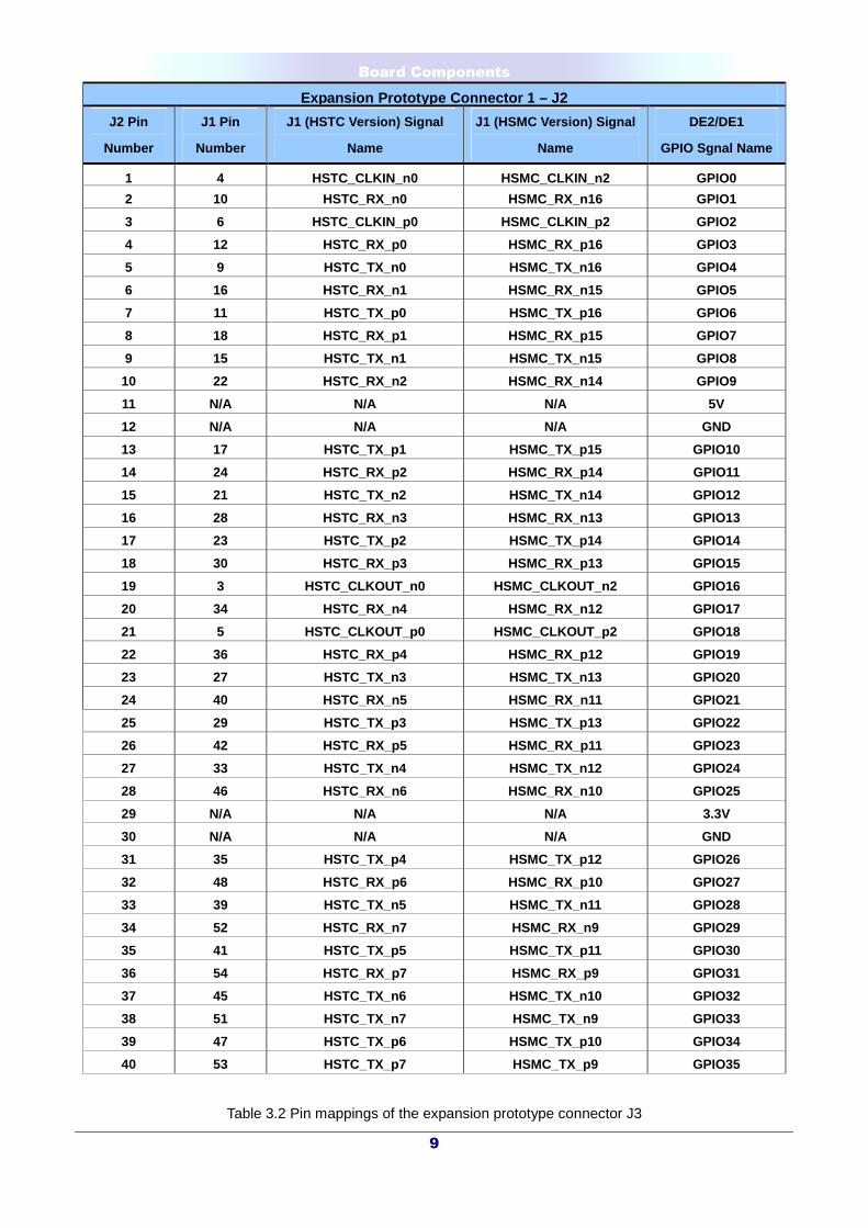
1-6Expansion Prototype Connectors
This section describes the expansion prototype connectors on the THDB-HTG board.
The THDB-HTG board has three expansion prototype connectors (J2, J3, and J4) connected to the
HSTC/HSMC connector directly. Each of the connectors has 36 prototyping I/Os and 3.3/5 volts power supply
from the HSTC/HSMC interface and on-board regulator. In addition, the expansion connector is compatible
with expansion headers of Altera DE1/DE2 board. Users can connect Altera DE2/DE1 development kits or
custom daughter boards to a HSTC/HSMC-interfaced host board. Figure 3.2 and Figure 3.3 show the pin-outs
of the expansion prototype connectors for HSTC and HSMC version, respectively. Detailed pin mappings to
HSTC/HSMC connector are listed in Table 3.1, Table 3.2, and Table 3.3.
1
3
5
7
9
11
13
15
17
19
21
23
25
27
29
31
33
35
37
39
2
4
6
8
10
12
14
16
18
20
22
24
26
28
30
32
34
36
38
40
HSTC_CLKIN_n0
HSTC_CLKIN_p0
HSTC_TX_n0
HSTC_TX_p0
HSTC_TX_n1
5V
HSTC_TX_p1
HSTC_TX_n2
HSTC_TX_p2
HSTC_CLKOUT_n0
HSTC_CLKOUT_p0
HSTC_TX_n3
HSTC_TX_p3
HSTC_TX_n4
3.3V
HSTC_TX_p4
HSTC_TX_n5
HSTC_TX_p5
HSTC_TX_n6
HSTC_TX_p6
HSTC_RX_n0
HSTC_RX_p0
HSTC_RX_n1
HSTC_RX_p1
HSTC_RX_n2
GND
HSTC_RX_p2
HSTC_RX_n3
HSTC_RX_p3
HSTC_RX_n4
HSTC_RX_p4
HSTC_RX_n5
HSTC_RX_p5
HSTC_RX_n6
GND
HSTC_RX_p6
HSTC_RX_n7
HSTC_RX_p7
HSTC_TX_n7
HSTC_TX_p7
J21
3
5
7
9
11
13
15
17
19
21
23
25
27
29
31
33
35
37
39
2
4
6
8
10
12
14
16
18
20
22
24
26
28
30
32
34
36
38
40
HSTC_CLKIN_n1
HSTC_CLKIN_p1
HSTC_TX_n9
HSTC_TX_p9
HSTC_TX_n10
5V
HSTC_TX_p10
HSTC_TX_n11
HSTC_TX_p11
HSTC_CLKOUT_n1
HSTC_CLKOUT_p1
HSTC_TX_n12
HSTC_TX_p12
HSTC_TX_n13
3.3V
HSTC_TX_p13
HSTC_TX_n14
HSTC_TX_p14
HSTC_TX_n15
HSTC_TX_p15
HSTC_RX_n9
HSTC_RX_p9
HSTC_RX_n10
HSTC_RX_p10
HSTC_RX_n11
GND
HSTC_RX_p11
HSTC_RX_n12
HSTC_RX_p12
HSTC_RX_n13
HSTC_RX_p13
HSTC_RX_n14
HSTC_RX_p14
HSTC_RX_n15
GND
HSTC_RX_p15
HSTC_RX_n16
HSTC_RX_p16
HSTC_TX_n16
HSTC_TX_p16
1
3
5
7
9
11
13
15
17
19
21
23
25
27
29
31
33
35
37
39
2
4
6
8
10
12
14
16
18
20
22
24
26
28
30
32
34
36
38
40
HSTC_TX_n18
HSTC_TX_p18
HSTC_TX_n19
HSTC_TX_p19
HSTC_TX_n20
5V
HSTC_TX_p20
HSTC_TX_n21
HSTC_TX_p21
HSTC_TX_n22
HSTC_TX_p22
HSTC_TX_n23
HSTC_TX_p23
HSTC_TX_n24
3.3V
HSTC_TX_p24
HSTC_TX_n25
HSTC_TX_p25
HSTC_TX_n26
HSTC_TX_p26
HSTC_RX_n18
HSTC_RX_p18
HSTC_RX_n19
HSTC_RX_p19
HSTC_RX_n20
GND
HSTC_RX_p20
HSTC_RX_n21
HSTC_RX_p21
HSTC_RX_n22
HSTC_RX_p22
HSTC_RX_n23
HSTC_RX_p23
HSTC_RX_n24
GND
HSTC_RX_p24
HSTC_RX_n26
HSTC_RX_p26
HSTC_RX_n25
HSTC_RX_p25
J3 J4
Figure 3.2 Pin-outs of the expansion prototype connectors for HSTC version
Board Components
8
Figure 3.3 Pin-outs of the expansion prototype connectors for HSMC version
Table 3.1 Pin mappings of the expansion prototype connector J2
Board Components
9
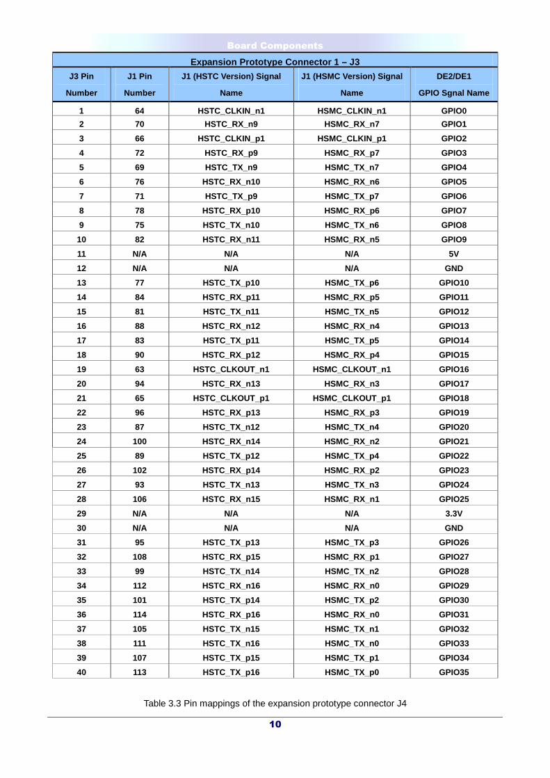
Expansion Prototype Connector 1 – J2
J2 Pin
Number
J1 Pin
Number
J1 (HSTC Version) Signal
Name
J1 (HSMC Version) Signal
Name
DE2/DE1
GPIO Sgnal Name
1 4 HSTC_CLKIN_n0 HSMC_CLKIN_n2 GPIO0
2 10 HSTC_RX_n0 HSMC_RX_n16 GPIO1
3 6 HSTC_CLKIN_p0 HSMC_CLKIN_p2 GPIO2
4 12 HSTC_RX_p0 HSMC_RX_p16 GPIO3
5 9 HSTC_TX_n0 HSMC_TX_n16 GPIO4
6 16 HSTC_RX_n1 HSMC_RX_n15 GPIO5
7 11 HSTC_TX_p0 HSMC_TX_p16 GPIO6
8 18 HSTC_RX_p1 HSMC_RX_p15 GPIO7
9 15 HSTC_TX_n1 HSMC_TX_n15 GPIO8
10 22 HSTC_RX_n2 HSMC_RX_n14 GPIO9
11 N/A N/A N/A 5V
12 N/A N/A N/A GND
13 17 HSTC_TX_p1 HSMC_TX_p15 GPIO10
14 24 HSTC_RX_p2 HSMC_RX_p14 GPIO11
15 21 HSTC_TX_n2 HSMC_TX_n14 GPIO12
16 28 HSTC_RX_n3 HSMC_RX_n13 GPIO13
17 23 HSTC_TX_p2 HSMC_TX_p14 GPIO14
18 30 HSTC_RX_p3 HSMC_RX_p13 GPIO15
19 3 HSTC_CLKOUT_n0 HSMC_CLKOUT_n2 GPIO16
20 34 HSTC_RX_n4 HSMC_RX_n12 GPIO17
21 5 HSTC_CLKOUT_p0 HSMC_CLKOUT_p2 GPIO18
22 36 HSTC_RX_p4 HSMC_RX_p12 GPIO19
23 27 HSTC_TX_n3 HSMC_TX_n13 GPIO20
24 40 HSTC_RX_n5 HSMC_RX_n11 GPIO21
25 29 HSTC_TX_p3 HSMC_TX_p13 GPIO22
26 42 HSTC_RX_p5 HSMC_RX_p11 GPIO23
27 33 HSTC_TX_n4 HSMC_TX_n12 GPIO24
28 46 HSTC_RX_n6 HSMC_RX_n10 GPIO25
29 N/A N/A N/A 3.3V
30 N/A N/A N/A GND
31 35 HSTC_TX_p4 HSMC_TX_p12 GPIO26
32 48 HSTC_RX_p6 HSMC_RX_p10 GPIO27
33 39 HSTC_TX_n5 HSMC_TX_n11 GPIO28
34 52 HSTC_RX_n7 HSMC_RX_n9 GPIO29
35 41 HSTC_TX_p5 HSMC_TX_p11 GPIO30
36 54 HSTC_RX_p7 HSMC_RX_p9 GPIO31
37 45 HSTC_TX_n6 HSMC_TX_n10 GPIO32
38 51 HSTC_TX_n7 HSMC_TX_n9 GPIO33
39 47 HSTC_TX_p6 HSMC_TX_p10 GPIO34
40 53 HSTC_TX_p7 HSMC_TX_p9 GPIO35
Table 3.2 Pin mappings of the expansion prototype connector J3
Board Components
10
Expansion Prototype Connector 1 – J3
J3 Pin
Number
J1 Pin
Number
J1 (HSTC Version) Signal
Name
J1 (HSMC Version) Signal
Name
DE2/DE1
GPIO Sgnal Name
1 64 HSTC_CLKIN_n1 HSMC_CLKIN_n1 GPIO0
2 70 HSTC_RX_n9 HSMC_RX_n7 GPIO1
3 66 HSTC_CLKIN_p1 HSMC_CLKIN_p1 GPIO2
4 72 HSTC_RX_p9 HSMC_RX_p7 GPIO3
5 69 HSTC_TX_n9 HSMC_TX_n7 GPIO4
6 76 HSTC_RX_n10 HSMC_RX_n6 GPIO5
7 71 HSTC_TX_p9 HSMC_TX_p7 GPIO6
8 78 HSTC_RX_p10 HSMC_RX_p6 GPIO7
9 75 HSTC_TX_n10 HSMC_TX_n6 GPIO8
10 82 HSTC_RX_n11 HSMC_RX_n5 GPIO9
11 N/A N/A N/A 5V
12 N/A N/A N/A GND
13 77 HSTC_TX_p10 HSMC_TX_p6 GPIO10
14 84 HSTC_RX_p11 HSMC_RX_p5 GPIO11
15 81 HSTC_TX_n11 HSMC_TX_n5 GPIO12
16 88 HSTC_RX_n12 HSMC_RX_n4 GPIO13
17 83 HSTC_TX_p11 HSMC_TX_p5 GPIO14
18 90 HSTC_RX_p12 HSMC_RX_p4 GPIO15
19 63 HSTC_CLKOUT_n1 HSMC_CLKOUT_n1 GPIO16
20 94 HSTC_RX_n13 HSMC_RX_n3 GPIO17
21 65 HSTC_CLKOUT_p1 HSMC_CLKOUT_p1 GPIO18
22 96 HSTC_RX_p13 HSMC_RX_p3 GPIO19
23 87 HSTC_TX_n12 HSMC_TX_n4 GPIO20
24 100 HSTC_RX_n14 HSMC_RX_n2 GPIO21
25 89 HSTC_TX_p12 HSMC_TX_p4 GPIO22
26 102 HSTC_RX_p14 HSMC_RX_p2 GPIO23
27 93 HSTC_TX_n13 HSMC_TX_n3 GPIO24
28 106 HSTC_RX_n15 HSMC_RX_n1 GPIO25
29 N/A N/A N/A 3.3V
30 N/A N/A N/A GND
31 95 HSTC_TX_p13 HSMC_TX_p3 GPIO26
32 108 HSTC_RX_p15 HSMC_RX_p1 GPIO27
33 99 HSTC_TX_n14 HSMC_TX_n2 GPIO28
34 112 HSTC_RX_n16 HSMC_RX_n0 GPIO29
35 101 HSTC_TX_p14 HSMC_TX_p2 GPIO30
36 114 HSTC_RX_p16 HSMC_RX_n0 GPIO31
37 105 HSTC_TX_n15 HSMC_TX_n1 GPIO32
38 111 HSTC_TX_n16 HSMC_TX_n0 GPIO33
39 107 HSTC_TX_p15 HSMC_TX_p1 GPIO34
40 113 HSTC_TX_p16 HSMC_TX_p0 GPIO35
Table 3.3 Pin mappings of the expansion prototype connector J4
Board Components
11
Expansion Prototype Connector 1 – J4
J4 Pin
Number
J1 Pin
Number
J1 (HSTC Version) Signal
Name
J1 (HSMC Version) Signal
Name
DE2/DE1
GPIO Sgnal Name
1 133 HSTC_TX_n18 ND GPIO0
2 134 HSTC_RX_n18 ND GPIO1
3 135 HSTC_TX_p18 HSMC_TXVR_TXn0 GPIO2
4 136 HSTC_RX_p18 HSMC_TXVR_RXn0 GPIO3
5 137 HSTC_TX_n19 HSMC_TXVR_TXp0 GPIO4
6 138 HSTC_RX_n19 HSMC_TXVR_RXp0 GPIO5
7 139 HSTC_TX_p19 ND GPIO6
8 140 HSTC_RX_p19 ND GPIO7
9 141 HSTC_TX_n20 HSMC_TXVR_TXn1 GPIO8
10 142 HSTC_RX_n20 HSMC_TXVR_RXn1 GPIO9
11 N/A N/A N/A 5V
12 N/A N/A N/A GND
13 143 HSTC_TX_p20 HSMC_TXVR_TXp1 GPIO10
14 144 HSTC_RX_p20 HSMC_TXVR_RXp1 GPIO11
15 145 HSTC_TX_n21 ND GPIO12
16 146 HSTC_RX_n21 ND GPIO13
17 147 HSTC_TX_p21 HSMC_TXVR_TXn2 GPIO14
18 148 HSTC_RX_p21 HSMC_TXVR_RXn2 GPIO15
19 149 HSTC_TX_n22 HSMC_TXVR_TXp2 GPIO16
20 150 HSTC_RX_n22 HSMC_TXVR_RXp2 GPIO17
21 151 HSTC_TX_p22 ND GPIO18
22 152 HSTC_RX_p22 ND GPIO19
23 153 HSTC_TX_n23 HSMC_TXVR_TXn3 GPIO20
24 154 HSTC_RX_n23 HSMC_TXVR_RXn3 GPIO21
25 155 HSTC_TX_p23 HSMC_TXVR_TXp3 GPIO22
26 156 HSTC_RX_p23 HSMC_TXVR_RXp3 GPIO23
27 157 HSTC_TX_n24 ND GPIO24
28 158 HSTC_RX_n24 ND GPIO25
29 N/A N/A N/A 3.3V
30 N/A N/A N/A GND
31 159 HSTC_TX_p24 HSMC_TXVR_TXn4 GPIO26
32 160 HSTC_RX_p24 HSMC_TXVR_RXn4 GPIO27
33 161 HSTC_TX_n25 HSMC_TXVR_TXp4 GPIO28
34 166 HSTC_RX_n26 HSMC_TXVR_RXn5 GPIO29
35 163 HSTC_TX_p25 ND GPIO30
36 168 HSTC_RX_p26 HSMC_TXVR_RXp5 GPIO31
37 165 HSTC_TX_n26 HSMC_TXVR_TXn5 GPIO32
38 162 HSTC_TX_n25 HSMC_TXVR_RXp4 GPIO33
39 167 HSTC_TX_p26 HSMC_TXVR_TXp5 GPIO34
40 164 HSTC_TX_p25 ND GPIO35

Board Components
12
1-7Cyclone III Starter Board HSMC Connector The naming convention used to assign the pin names for the HSMC connector is different for the Cyclone III
Starter Board and the standard HSMC connector. Figure 3.4 shows the pin-outs of the expansion prototype
connectors for Cyclone III Starter board HSMC version.
Figure 3.4 Pin-outs of the expansion prototype connectors for Cyclone III Starter board HSMC version
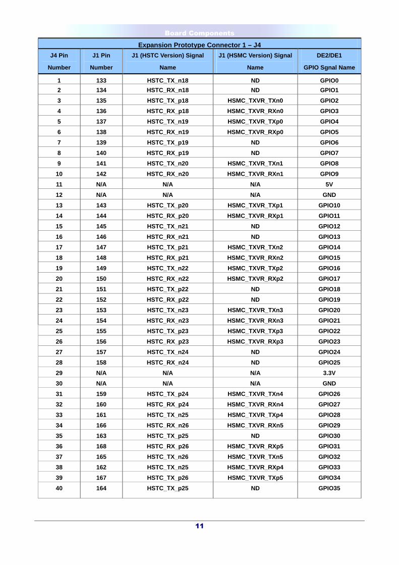
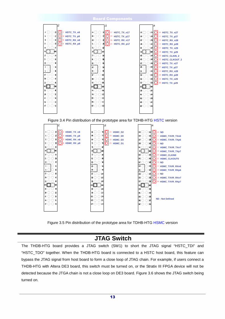
1-8Prototyping Area The THDB-HTG board provides users a prototyping area for signal measurement or debug. These
prototyping points are connected to the HSTC/HSMC connector directly. Detailed I/O maps for HSTC and
HSMC version are provided to help users locate the corresponding prototyping points, as shown in Figure 3.4
and Figures 3.5, respectively.
Board Components
13
HSTC_TX_n8
HSTC_TX_p8
HSTC_RX_n8
HSTC_RX_p8
HSTC_TX_n17
HSTC_TX_p17
HSTC_RX_n17
HSTC_RX_p17
HSTC_TX_n27
HSTC_TX_p27
HSTC_RX_n28
HSTC_RX_p28
HSTC_TX_n29
HSTC_TX_p29
HSTC_CLKIN_2
HSTC_CLKOUT_2
HSTC_TX_n27
HSTC_TX_p27
HSTC_RX_n28
HSTC_RX_p28
HSTC_TX_n29
HSTC_TX_p29
Figure 3.4 Pin distribution of the prototype area for TDHB-HTG HSTC version
HSMC_TX_n8
HSMC_TX_p8
HSMC_RX_n8
HSMC_RX_p8
HSMC_D2
HSMC_D0
HSMC_D3
HSMC_D1
ND
HSMC_TXVR_TXn6
HSMC_TXVR_TXp6
ND
HSMC_TXVR_TXn7
HSMC_TXVR_TXp7
HSMC_CLKIN0
HSMC_CLKOUT0
ND
HSMC_TXVR_RXn6
HSMC_TXVR_RXp6
ND
HSMC_TXVR_RXn7
HSMC_TXVR_RXp7
ND : Not Defined
Figure 3.5 Pin distribution of the prototype area for TDHB-HTG HSMC version
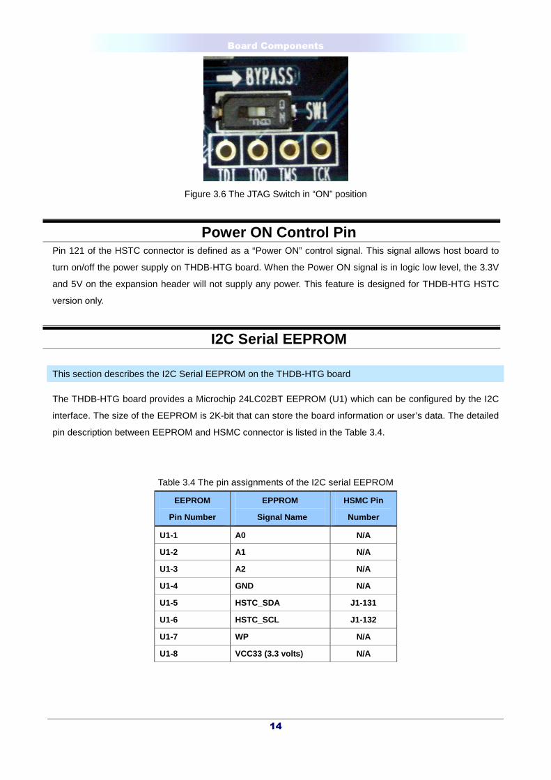
1-9JTAG Switch The THDB-HTG board provides a JTAG switch (SW1) to short the JTAG signal “HSTC_TDI” and
“HSTC_TDO” together. When the THDB-HTG board is connected to a HSTC host board, this feature can
bypass the JTAG signal from host board to form a close loop of JTAG chain. For example, if users connect a
THDB-HTG with Altera DE3 board, this switch must be turned on, or the Stratix III FPGA device will not be
detected because the JTGA chain is not a close loop on DE3 board. Figure 3.6 shows the JTAG switch being
turned on.
Board Components
14
Figure 3.6 The JTAG Switch in “ON” position
1-10Power ON Control Pin Pin 121 of the HSTC connector is defined as a “Power ON” control signal. This signal allows host board to
turn on/off the power supply on THDB-HTG board. When the Power ON signal is in logic low level, the 3.3V
and 5V on the expansion header will not supply any power. This feature is designed for THDB-HTG HSTC
version only.
1-11I2C Serial EEPROM
This section describes the I2C Serial EEPROM on the THDB-HTG board
The THDB-HTG board provides a Microchip 24LC02BT EEPROM (U1) which can be configured by the I2C
interface. The size of the EEPROM is 2K-bit that can store the board information or user’s data. The detailed
pin description between EEPROM and HSMC connector is listed in the Table 3.4.
Table 3.4 The pin assignments of the I2C serial EEPROM
EEPROM
Pin Number
EPPROM
Signal Name
HSMC Pin
Number
U1-1 A0 N/A
U1-2 A1 N/A
U1-3 A2 N/A
U1-4 GND N/A
U1-5 HSTC_SDA J1-131
U1-6 HSTC_SCL J1-132
U1-7 WP N/A
U1-8 VCC33 (3.3 volts) N/A
Board Components
15
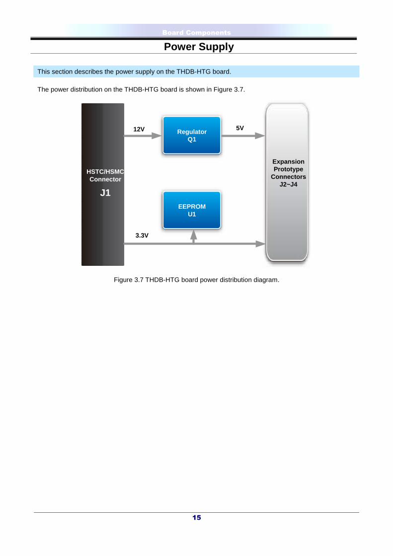
1-12Power Supply
This section describes the power supply on the THDB-HTG board.
The power distribution on the THDB-HTG board is shown in Figure 3.7.
EEPROMU1
12V
J1
RegulatorQ1
5V
ExpansionPrototype
ConnectorsJ2~J4
3.3V
HSTC/HSMCConnector
Figure 3.7 THDB-HTG board power distribution diagram.

Demonstration
16
4
Demonstration This chapter illustrates how to use the THDB-HTG board to a HSMC-interfaced host board.
1-13Connecting THDB-HTG Board to a Cyclone III Starter Board
This section describes how to use the THDB-HTG board with a Cyclone III Starter Board.
Figure 4.1 illustrates how the THDB-HTG board is connected to the Cyclone III starter board. Users need to
pay extra attention to the following two points:
1. Observe the orientation of the HSMC connector when connecting the THDB-HTG to the Cyclone
III Starter Board.
2. Note that there are two LVDS pairs on the HSMC connector: the HSMC_CLK_p1/n1 (form a close
loop via R3) and HSMC_CLKIN_p2/n2 (form a close loop via R4). Therefore, using any one of the
signal in a LVDS pair under single-ended mode will prevent users from using the other signal in the
same pair.
Figure 4.1 Connecting the THDB-HTG board to the Cyclone III starter board
Demonstration
17
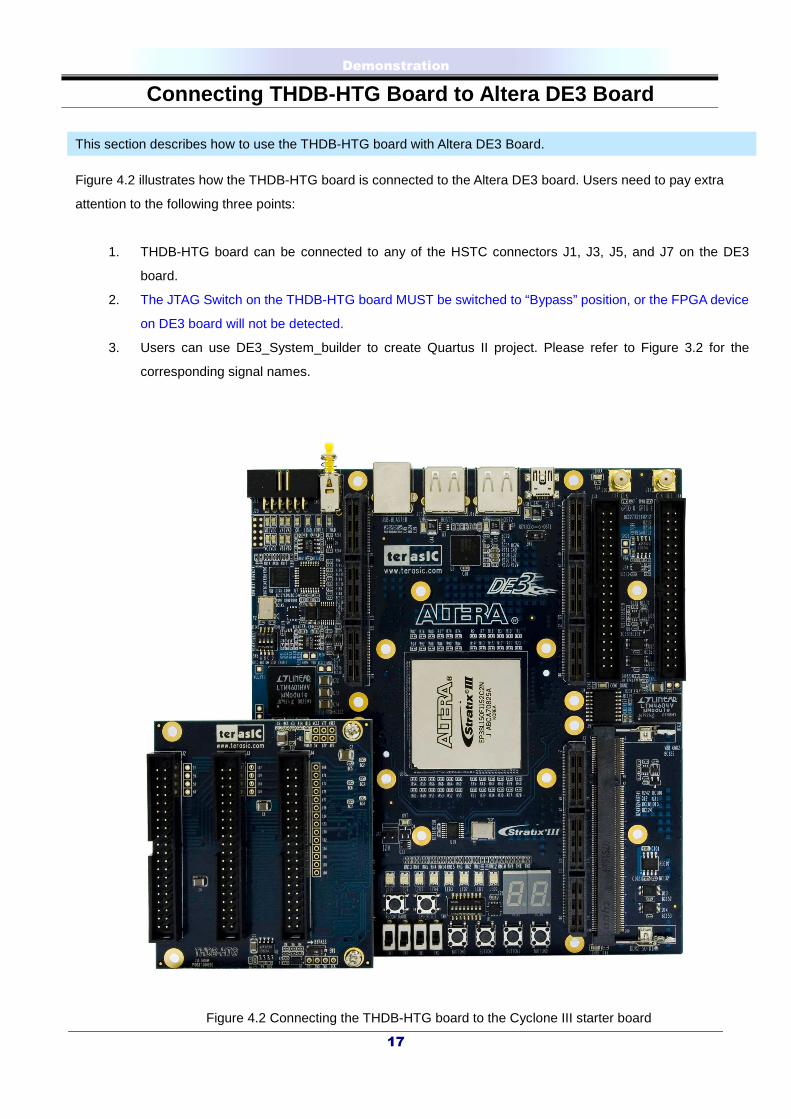
1-14Connecting THDB-HTG Board to Altera DE3 Board
This section describes how to use the THDB-HTG board with Altera DE3 Board.
Figure 4.2 illustrates how the THDB-HTG board is connected to the Altera DE3 board. Users need to pay extra
attention to the following three points:
1. THDB-HTG board can be connected to any of the HSTC connectors J1, J3, J5, and J7 on the DE3
board.
2. The JTAG Switch on the THDB-HTG board MUST be switched to “Bypass” position, or the FPGA device
on DE3 board will not be detected.
3. Users can use DE3_System_builder to create Quartus II project. Please refer to Figure 3.2 for the
corresponding signal names.
Figure 4.2 Connecting the THDB-HTG board to the Cyclone III starter board
Appendix
18
5
Appendix
1-15Revision History
Date Change Log
JAN 04, 2009 Initial Version
Oct 20, 2009 Added Cyclone III Starter Board HSMC Connector section
April 08, 2010 Modified pin names for Cyclone III Starter Board HSMC Connector
section
1-16Always Visit THDB-HTG Webpage for New Main board
We will be continuing providing interesting examples and labs on our THDB-HTG
webpage. Please visit www.altera.com or HTG.terasic.com for more information.


