P A R T N E R S L L C P RISMAR K TEST ACCESS TO TODAY’S LEADING PACKAGES February 28, 2000 P REPARED B Y : Charles L. Lassen PRISMARK PARTNERS LLC 130 Main Street Cold Spring Harbor NY 11724 Tel: 516 367-9187 Fax: 516 367-9223 e-mail: [email protected]www.prismark.com 20Test.cll
Transcript
P A R T N E R S L L CPRISMARK
TEST ACCESS TO TODAY’S LEADING PACKAGES
February 28, 2000
PREPARED BY:
Charles L. LassenPRISMARK PARTNERS LLC
130 Main Street Cold Spring Harbor NY 11724Tel: 516 367-9187 Fax: 516 367-9223
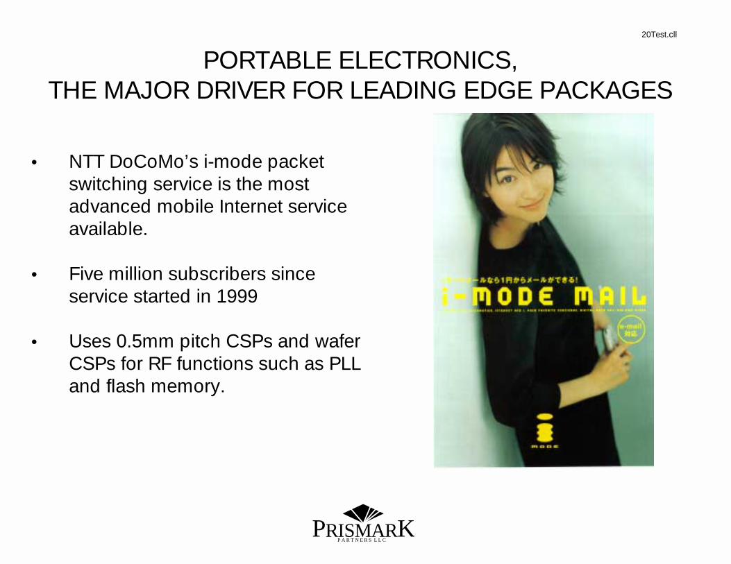
PORTABLE ELECTRONICS,THE MAJOR DRIVER FOR LEADING EDGE PACKAGES
• NTT DoCoMo’s i-mode packetswitching service is the mostadvanced mobile Internet serviceavailable.
• Five million subscribers sinceservice started in 1999
• Uses 0.5mm pitch CSPs and waferCSPs for RF functions such as PLLand flash memory.
P A R T N E R S L L CPRISMARK
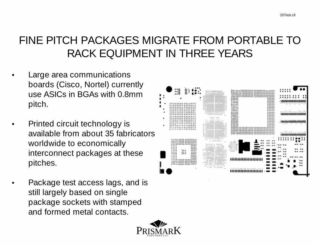
FINE PITCH PACKAGES MIGRATE FROM PORTABLE TORACK EQUIPMENT IN THREE YEARS
• Large area communicationsboards (Cisco, Nortel) currentlyuse ASICs in BGAs with 0.8mmpitch.
• Printed circuit technology isavailable from about 35 fabricatorsworldwide to economicallyinterconnect packages at thesepitches.
• Package test access lags, and isstill largely based on singlepackage sockets with stampedand formed metal contacts.
20Test.cll
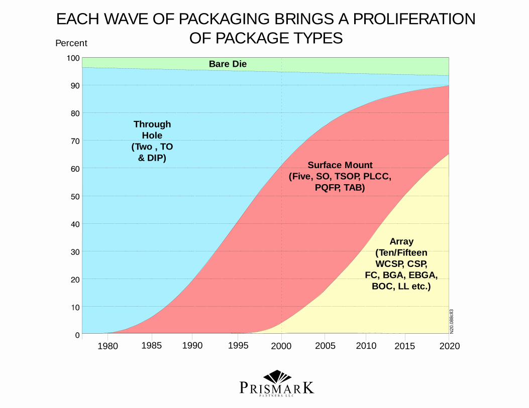
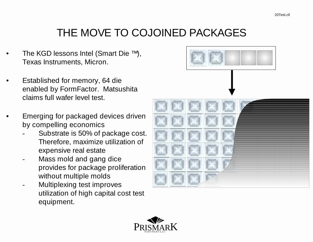
EACH WAVE OF PACKAGING BRINGS A PROLIFERATIONOF PACKAGE TYPES
1980 1985 1990 1995 2000 2005 2010 2015 2020
Percent
Bare Die
Through Hole
(Two , TO& DIP)
Surface Mount(Five, SO, TSOP, PLCC,
PQFP, TAB)
Array(Ten/FifteenWCSP, CSP,
FC, BGA, EBGA,BOC, LL etc.)
N20
.088
cll3
30%
25%
20%
15%
10%
5%
0%
<16 16-28 29-48 49-84 85-120
Leadcount
121-256 257-356 357-550 >550
N20
.088
cll1
Array Packages(3%)
90% of allSilicon hasless than100 I/O
Bare Die(7%)
Through Hole(26%)
SMT(64%)
LOW LEADCOUNT STILL DOMINATES SILICON“Market Share” by Leadcount and Package Type 1999
P A R T N E R S L L CPRISMARK
CHIP SCALE PACKAGES IN THE T28 BASEBAND SECTION
• Only one PCB assembly
– 6 layer microvia from Suzuki– 125 µm laser vias, 110 µm lines– 30 attachment pads per cm2
• Five CSP in baseband section
1. Wirebond-on-flex CSP (Signal Processor)
• 12 x 12 mm, 1.2 mm total height• 132 balls, 0.8 mm pitch• Underfilled
2. Wirebond-on-Flex CSP (SRAM)• 8 x 8 mm, 1.3 mm total height• 64 balls, 0.8 mm pitch
3. Tessera-type µBGA CSP (Flash)
• 7 x 7 mm, 1.0 mm total height• 48 balls, 0.8 mm pitch• Underfilled
4. Wirebond-on Rigid CSP (ASIC)
• 8 x 8 mm, 1.5 mm total height• 64 balls, 0.8 mm pitch
5. Wirebond-on-Rigid CSP (ASIC)
• 8 x 8 mm, 1.5 mm total height• 64 balls, 0.8 mm pitch
20.087mvc
1
3 4
2
5
P A R T N E R S L L CPRISMARK
ERICSSON ASIC IN T28 PHONE
Wirebond-on-rigid CSP
Gang mold & dice
− 8 x 8 mm− 1.5 mm total height− 64 balls, 0.8 mm pitch− No underfill
20.087mvc
P A R T N E R S L L CPRISMARK
RF MODULE INTEGRATION IN THE T28 PHONE
• Ericsson Receiver– 64 lead QFP, 0.4 mm pitch
• Conexant Power Amplifier– 9.1 x 11.6 x 1.6 mm– 4 layer BT PCB carrier– Wirebonded die and SMT
passives
• Murata Switchplexer– 6.7 x 5.0 x 2.0 mm– LTCC with integrated passives– SMT passives on top
• National Semiconductor VCO IC– 3.5 x 3.5 x 1.3 mm– Wirebond-on-rigid CSP– 16 external pads, no balls
20.087cll
Power Amplifier
AntennaConnection
Switchplexer
VCO
Filter
Inductor
Receiver
VCO
P A R T N E R S L L CPRISMARK
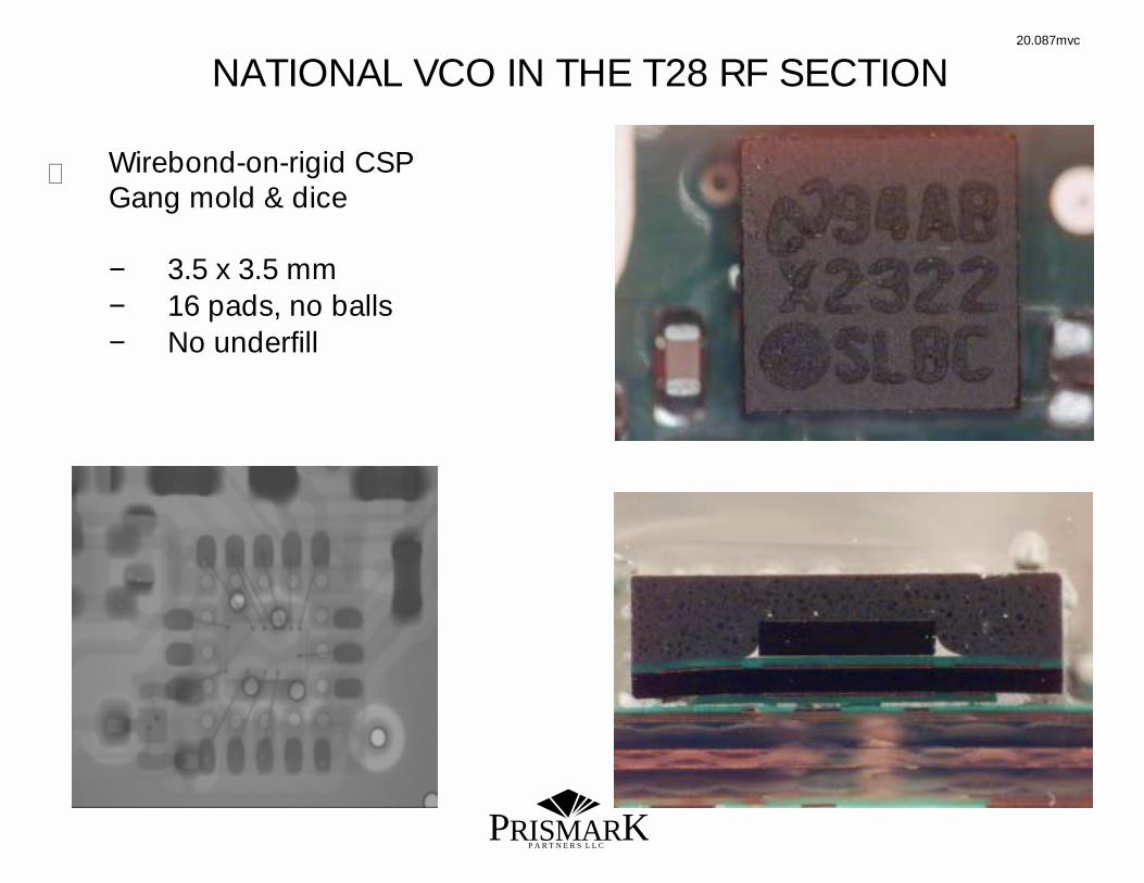
NATIONAL VCO IN THE T28 RF SECTION
Wirebond-on-rigid CSP
Gang mold & dice
− 3.5 x 3.5 mm− 16 pads, no balls− No underfill
20.087mvc
P A R T N E R S L L CPRISMARK
CONEXANT
• Components GaAs PA with integrated resistors CMOS interface die 9-16 wirebonds each 19 discrete passives, 0402 size (one 0603)
• Integrated Passives All resistors on GaAs die (cost, design flexibility) Low value inductors (<10 nH) integrated on carrier High Q passives for output match better as
discretes Multilayer carrier provides free layers for passive
integration Microvia may allow further integration
• Just started shipping in Ericsson T28 dual-band GSMphone.
1090241mvc
PACKAGE COST DOMAINSOne Million Pieces per Month - September 1999
0
Source: Prismark’s Quarterly Packaging Report and Survey.Note: All packaging costs, excluding silicon.
10 100
Leadcount
1000
0.5
1.0
1.5
2.0
3.0
2.5
3.5
Cents Per Lead
PerformanceFlip Chip
PBGA
PerformanceMemory
Work Horse PBGA
Wafer CSPLeadframe
N20
.088
cll2
MidRangeTBGA
P A R T N E R S L L CPRISMARK
20.085CLL
Dallas Semiconductors
National Semiconductor
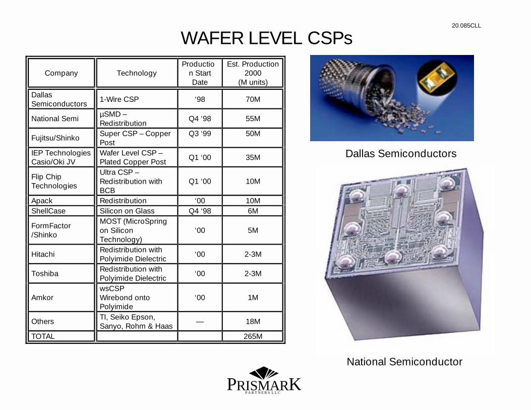
WAFER LEVEL CSPs
Company TechnologyProductio
n StartDate
Est. Production2000
(M units)
DallasSemiconductors
1-Wire CSP ‘98 70M
National Semi µSMD –Redistribution
Q4 ‘98 55M
Fujitsu/Shinko Super CSP – CopperPost
Q3 ‘99 50M
IEP TechnologiesCasio/Oki JV
Wafer Level CSP –Plated Copper Post Q1 ‘00 35M
Flip ChipTechnologies
Ultra CSP –Redistribution withBCB
Q1 ‘00 10M
Apack Redistribution ‘00 10MShellCase Silicon on Glass Q4 ‘98 6M
FormFactor/Shinko
MOST (MicroSpringon SiliconTechnology)
‘00 5M
Hitachi Redistribution withPolyimide Dielectric
‘00 2-3M
Toshiba Redistribution withPolyimide Dielectric
‘00 2-3M
AmkorwsCSPWirebond ontoPolyimide
‘00 1M
Others TI, Seiko Epson,Sanyo, Rohm & Haas
— 18M
TOTAL 265M
P A R T N E R S L L CPRISMARK
119086/076bp
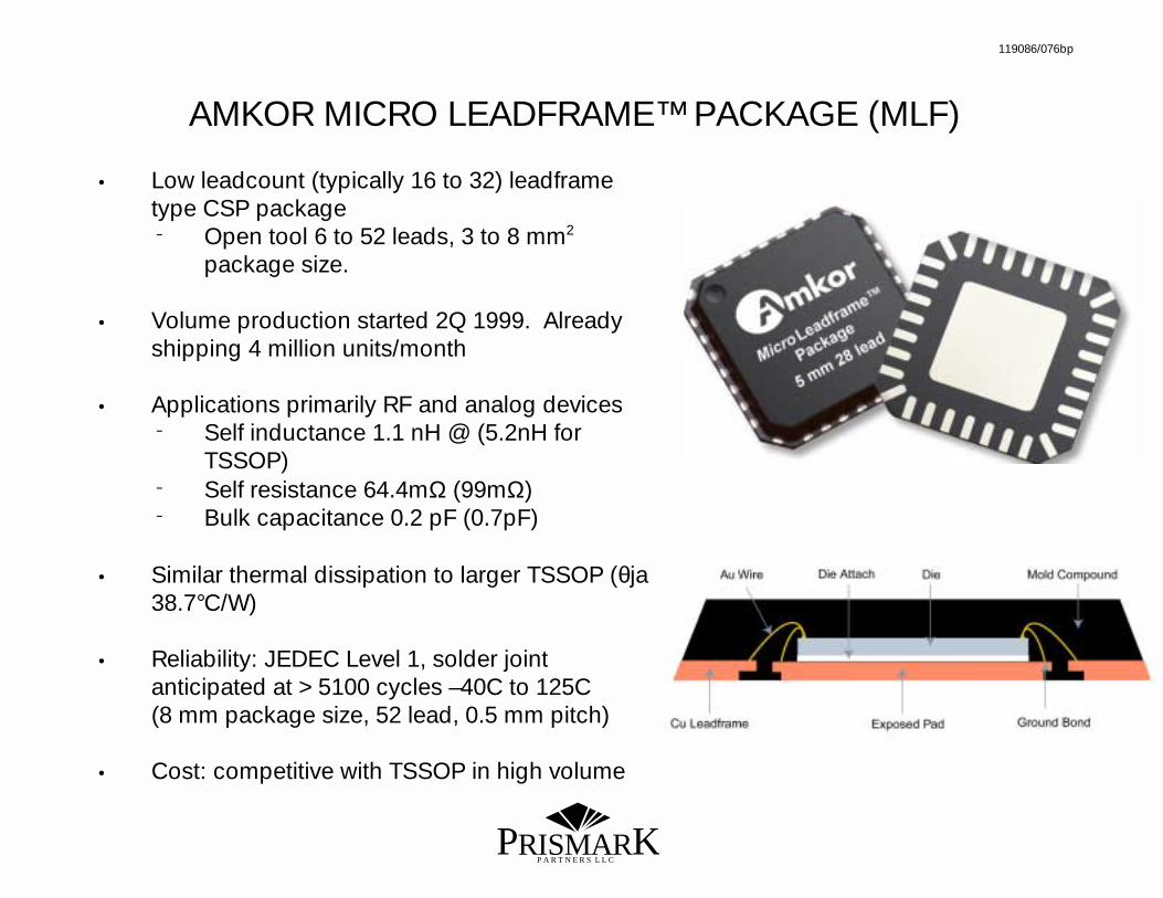
AMKOR MICRO LEADFRAME™ PACKAGE (MLF)
• Low leadcount (typically 16 to 32) leadframetype CSP package Open tool 6 to 52 leads, 3 to 8 mm2
package size.
• Volume production started 2Q 1999. Alreadyshipping 4 million units/month
• Applications primarily RF and analog devices Self inductance 1.1 nH @ (5.2nH for
• Similar thermal dissipation to larger TSSOP (θja38.7°C/W)
• Reliability: JEDEC Level 1, solder jointanticipated at >5100 cycles –40C to 125C(8 mm package size, 52 lead, 0.5 mm pitch)
• Cost: competitive with TSSOP in high volume
P A R T N E R S L L CPRISMARK
AMKOR CHIPARRAY® CSP
• Uses standard BGA assembly with 2layer BT substrate
• Targets devices with pincounts from 32to 208.
• Current applications are ASICs, PLDs,and others such as memory (flash), RF,and analog devices in portableequipment.
• Most production at 1.0 and 0.8 mmpitch, but some products now movingto 0.5 mm.
69086bp
3M ENHANCED CSP CE-CSP
• Enhanced CSP constructed bylaminating patterned 5-mil copperleadframe to the flex circuit.− IC attach to leadframe− IC is wirebonded through slots in