Page 1
8/6/2019 Testability of Integrated Systems
http://slidepdf.com/reader/full/testability-of-integrated-systems 1/24
Design Testability of Integrated systems
Butterfly’ s Page 1
Contents
1. Design Constraints 1.1 Design Rule Checking
1.2 Layout versus Schematic
1.3 Latch-Up and Electro-Static
Discharge
1.4 Electrical Rule Checking
2. Testing
3. The Rule of Ten
4. Terminology
5. Failures in CMOS
6. Combinational Logic Testing
6.1 Sensitized Path Testing
7. Practical Ad-Hoc DFT Guidelines
7.1 Improve Controllability and
Observability
7.2 Use Multiplexers
7.3 Partition Large Circuits
7.4 Divide Long Counter Chains
7.5 Initialize Sequential Logic
7.6 Avoid Asynchronous Logic
7.7 Avoid Logical Redundancy
7.8 Avoid Delay Dependent Logic
7.9 Strictly Distinguish Between
Signal and Clock
7.10 Avoid Self Resetting Logic
7.11 Use Bused Structure
7.12 Separate Analog and
Digital Circuits
7.13 Bypassing Techniques
8. Scan Design Techniques
8.1 Scan Path
8.2 Boundary Scan Test (BST)
Page 2
8/6/2019 Testability of Integrated Systems
http://slidepdf.com/reader/full/testability-of-integrated-systems 2/24
Design Testability of Integrated systems
Butterfly’ s Page 2
Testability of Integrated Systems
1. Design Constraints
The following paragraphs remind the designer of some basic rules to consider beforestarting. Each of these constraints has at least one tool helping in the development of the
design in respect to a set of rules:
1.1 Design Rule Checking
Every technology has its design rules. It consists in interpreting the possible
geometrical implementation of the chips to be manufactured. These rules are given by the
technology department in every foundry of IC. Rules are often described in a document with
boxes representing the layers available in the technology on which are indicated the sizes,
distances and geometrical constraints allowed in this technology.
Figure-1
Designer needs to execute a program called DRC to check whether his design adheres
to the rules defined by the founder. This step of verification called DRC is as important as the
simulation of the functionality of your design. A sole simulation can't take in consideration if the rules are respected in which case the manufacturing of the chip could lead to shorts or
cuts in the silicon physical implementation. Some other verification tools should also be used,
such as ERC and LVS described above.
1.2 Layout versus Schematic
As a complement to the DRC, LVS is another tool to be used especially if the design started
with a Schematic Entry tool.
Page 3
8/6/2019 Testability of Integrated Systems
http://slidepdf.com/reader/full/testability-of-integrated-systems 3/24
Design Testability of Integrated systems
Butterfly’ s Page 3
The aim of LVS is to check if the design at the layout level corresponds or is still coherent to
the schematic.
Usually, designers start with a schematic and then simulate it, if it is OK then they go to
layout. But in some cases like full-custom or some semi-custom designs the layout
implementation of the chip differs from the schematic because of some simulation results or
because of a design error that simulation can't detect easily simulation could never be
exhaustive. LVS checks that the designer did the same representation at the schematic and
layout levels, if not LVS tools indicate the occurrence. Of course a simulation of the layout
using the same stimuli used for the schematic is more secure for the final design.
1.3 Latch-Up and Electro-Static Discharge
Latch-up caused to CMOS the early problems that delayed its introduction in the
electronic industry. It also called "Thyristor effect" and could cause the destruction of the chip
or a part of it. There are no real solution to this phenomena but a set of design techniques
exist to avoid instead of solving Latch-up occurrence. The origin of Latch-up is the
distribution of the NMOS and PMOS N and P basic structures inside the silicon. In some cases,
not only PN junction are formed but also a structure like PNPN or NPNP parasitic thyristors.
these parasitic elements could feature like a real thyristor and develop a high current
destroying the area around it including the PMOS and NMOS transistors.
The most used technique in avoiding the formation of such a structure is to add
"butting contact" polarising the N-well (or P-well) to Vdd (or to Ground). This technique
cannot eliminate the Latch-up process but reduces its effect.
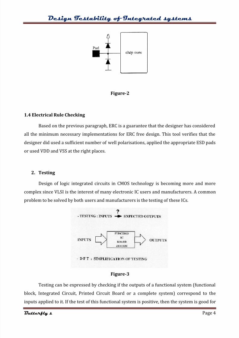
Another electrical constraint to CMOS is called ESD or Electro-Static Discharge.
Handling CMOS chip properly could be a solution to avoid gates destruction caused by
electro- static charges that people could have at the surface of their hands. This is the reason
why it is important to have a conducting bracelet linked to ground when handling CMOS ICs.
But even ground linked bracelet is not enough to protect CMOS chips from destruction due to
ESD. Two diodes at each pad inside the chip link every I/O to Vdd and Gnd. These two big
diodes protect the chip core (CMOS transistor gates) from ESD by limiting over-voltage.
Page 4
8/6/2019 Testability of Integrated Systems
http://slidepdf.com/reader/full/testability-of-integrated-systems 4/24
Design Testability of Integrated systems
Butterfly’ s Page 4
Figure-2
1.4 Electrical Rule Checking
Based on the previous paragraph, ERC is a guarantee that the designer has considered
all the minimum necessary implementations for ERC free design. This tool verifies that the
designer did used a sufficient number of well polarisations, applied the appropriate ESD pads
or used VDD and VSS at the right places.
2. Testing
Design of logic integrated circuits in CMOS technology is becoming more and more
complex since VLSI is the interest of many electronic IC users and manufacturers. A common
problem to be solved by both users and manufacturers is the testing of these ICs.
Figure-3
Testing can be expressed by checking if the outputs of a functional system (functional
block, Integrated Circuit, Printed Circuit Board or a complete system) correspond to the
inputs applied to it. If the test of this functional system is positive, then the system is good for
Page 5
8/6/2019 Testability of Integrated Systems
http://slidepdf.com/reader/full/testability-of-integrated-systems 5/24
Design Testability of Integrated systems
Butterfly’ s Page 5
use. If the outputs are different than expected, then the system has a problem: so either the
system is rejected (Go/No Go test), or a diagnosis is applied to it, in order to point out and
probably eliminate the problem's causes.
Testing is applied to detect faults after several operations : design, manufacturing, packaging
and especially during the active life of a system, and thus since failures caused by wear-out
can occur at any moment of its usage.
Design for Testability (DfT) is the ability of simplifying the test of any system. DfT could be
synthesized by a set of techniques and design guidelines where the goals are :
minimizing costs of system production
minimizing system test complexity : test generation and application
improving quality
avoiding problems of timing discordance or block nature incompatibility.
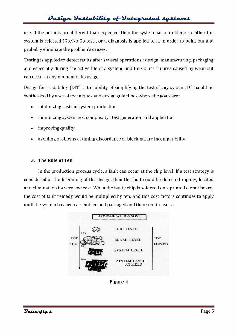
3. The Rule of Ten
In the production process cycle, a fault can occur at the chip level. If a test strategy is
considered at the beginning of the design, then the fault could be detected rapidly, located
and eliminated at a very low cost. When the faulty chip is soldered on a printed circuit board,
the cost of fault remedy would be multiplied by ten. And this cost factors continues to apply
until the system has been assembled and packaged and then sent to users.
Figure-4
Page 6
8/6/2019 Testability of Integrated Systems
http://slidepdf.com/reader/full/testability-of-integrated-systems 6/24
Design Testability of Integrated systems
Butterfly’ s Page 6
4. Terminology
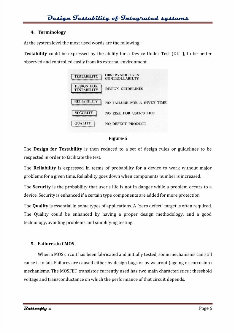
At the system level the most used words are the following:
Testability could be expressed by the ability for a Device Under Test (DUT), to be better
observed and controlled easily from its external environment.
Figure-5
The Design for Testability is then reduced to a set of design rules or guidelines to be
respected in order to facilitate the test.
The Reliability is expressed in terms of probability for a device to work without major
problems for a given time. Reliability goes down when components number is increased.
The Security is the probability that user's life is not in danger while a problem occurs to a
device. Security is enhanced if a certain type components are added for more protection.
The Quality is essential in some types of applications. A "zero defect" target is often required.
The Quality could be enhanced by having a proper design methodology, and a good
technology, avoiding problems and simplifying testing.
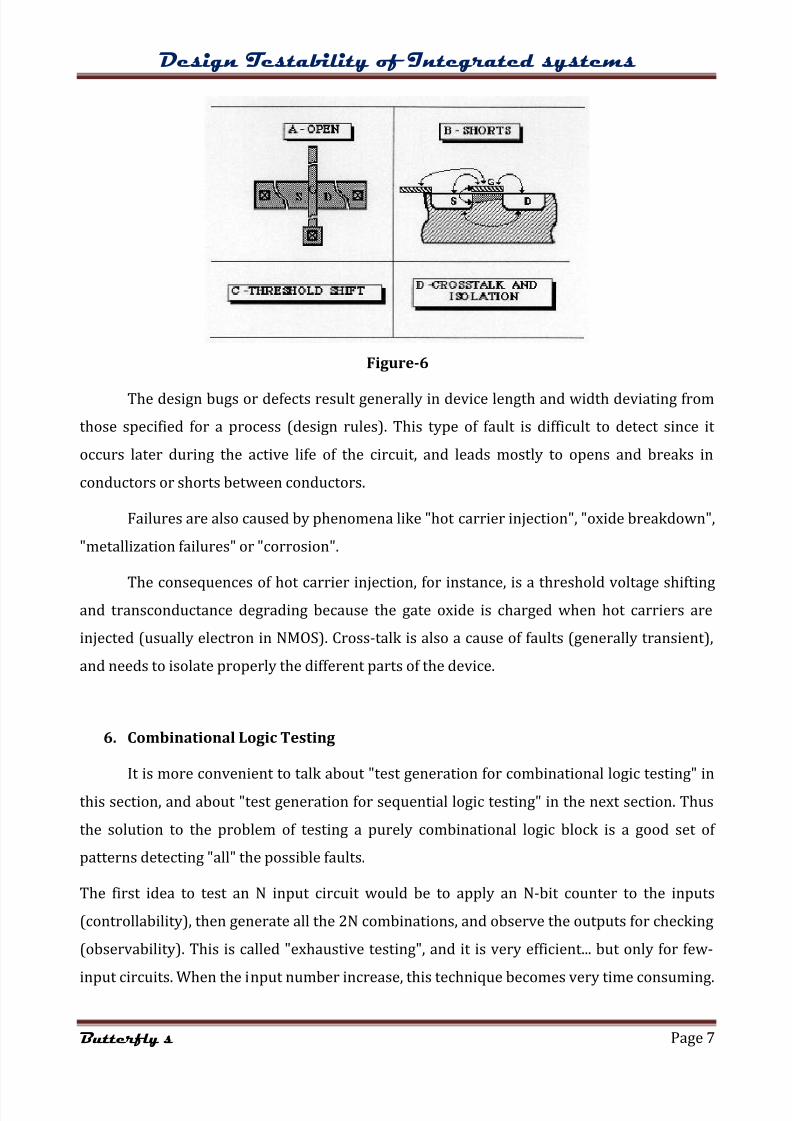
5. Failures in CMOS
When a MOS circuit has been fabricated and initially tested, some mechanisms can still
cause it to fail. Failures are caused either by design bugs or by wearout (ageing or corrosion)
mechanisms. The MOSFET transistor currently used has two main characteristics : threshold
voltage and transconductance on which the performance of that circuit depends.
Page 7
8/6/2019 Testability of Integrated Systems
http://slidepdf.com/reader/full/testability-of-integrated-systems 7/24
Design Testability of Integrated systems
Butterfly’ s Page 7
Figure-6
The design bugs or defects result generally in device length and width deviating from
those specified for a process (design rules). This type of fault is difficult to detect since it
occurs later during the active life of the circuit, and leads mostly to opens and breaks in
conductors or shorts between conductors.
Failures are also caused by phenomena like "hot carrier injection", "oxide breakdown",
"metallization failures" or "corrosion".
The consequences of hot carrier injection, for instance, is a threshold voltage shiftingand transconductance degrading because the gate oxide is charged when hot carriers are
injected (usually electron in NMOS). Cross-talk is also a cause of faults (generally transient),
and needs to isolate properly the different parts of the device.
6. Combinational Logic Testing
It is more convenient to talk about "test generation for combinational logic testing" in
this section, and about "test generation for sequential logic testing" in the next section. Thus
the solution to the problem of testing a purely combinational logic block is a good set of
patterns detecting "all" the possible faults.
The first idea to test an N input circuit would be to apply an N-bit counter to the inputs
(controllability), then generate all the 2N combinations, and observe the outputs for checking
(observability). This is called "exhaustive testing", and it is very efficient... but only for few-
input circuits. When the input number increase, this technique becomes very time consuming.
Page 8
8/6/2019 Testability of Integrated Systems
http://slidepdf.com/reader/full/testability-of-integrated-systems 8/24
Design Testability of Integrated systems
Butterfly’ s Page 8
Figure-7
6.1 Sensitized Path Testing
Most of the time, in exhaustive testing, many patterns do not occur during the
application of the circuit. So instead of spending a huge amount of time searching for faults
everywhere, the possible faults are first enumerated and a set of appropriate vectors are then
generated. This is called "single-path sensitization" and it is based on "fault oriented testing".
Figure-8
The basic idea is to select a path from the site of a fault, through a sequence of gates leading to
an output of the combinational logic under test. The process is composed of three steps :
Manifestation : gate inputs, at the site of the fault, are specified as to generate the
opposite value of the faulty value (0 for SA1, 1 for SA0).
Propagation : inputs of the other gates are determined so as to propagate the fault
signal along the specified path to the primary output of the circuit. This is done by
setting these inputs to "1" for AND/NAND gates and "0" for OR/NOR gates.
Page 9
8/6/2019 Testability of Integrated Systems
http://slidepdf.com/reader/full/testability-of-integrated-systems 9/24
Design Testability of Integrated systems
Butterfly’ s Page 9
Consistency : or justification. This final step helps finding the primary input pattern
that will realize all the necessary input values. This is done by tracing backward from
the gate inputs to the primary inputs of the logic in order to receive the test patterns.
Figure-9
EXAMPLE1 - SA1 of line1 (L1) : the aim is to find the vector(s) able to detect this fault.
Manifestation : L1 = 0 , then input A = 0. In a fault-free situation, the output F changes
with A if B,C and D are fixed : for B,C and D fixed, L1 is SA1 gives F = 0, for instance,
even if A = 0 (F = 1 for fault-free).
Propagation : Through the AND-gate : L5 = L8 = 1, this condition is necessary for the
propagation of the " L1 = 0 ". This leads to L10 = 0. Through the NOR-gate, and since
L10 = 0, then L11 = 0, so the propagated manifestation can reach the primary output F.
F is then read and compared with the fault-free value : F = 1.
Consistency : From the AND-gate : L5=1, and then L2=B=1. Also L8=1, and then L7=1.
Until now we found the values of A and B. When C and D are found, then the test
vectors are generated, in the same manner, and ready to be applied to detect L1= SA1.
From the NOT-gate, L11=0, so L9=L7=1 (coherency with L8=L7). From the OR-gate
L7=1, and since L6=L2=B=1, so B+C+D=L7=1, then C and D can have either 1 or 0.
These three steps have led to four possible vectors detecting L1=SA1.
Page 10
8/6/2019 Testability of Integrated Systems
http://slidepdf.com/reader/full/testability-of-integrated-systems 10/24
Design Testability of Integrated systems
Butterfly’ s Page 10
Figure-10
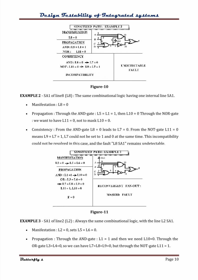
EXAMPLE 2 - SA1 of line8 (L8) : The same combinational logic having one internal line SA1.
Manifestation : L8 = 0
Propagation : Through the AND-gate : L5 = L1 = 1, then L10 = 0 Through the NOR-gate
: we want to have L11 = 0, not to mask L10 = 0.
Consistency : From the AND-gate L8 = 0 leads to L7 = 0. From the NOT-gate L11 = 0
means L9 = L7 = 1, L7 could not be set to 1 and 0 at the same time. This incompatibility
could not be resolved in this case, and the fault "L8 SA1" remains undetectable.
Figure-11
EXAMPLE 3 - SA1 of line2 (L2) : Always the same combinational logic, with the line L2 SA1.
Manifestation : L2 = 0, sets L5 = L6 = 0.
Propagation : Through the AND-gate : L1 = 1 and then we need L10=0. Through the
OR-gate L3=L4=0, so we can have L7=L8=L9=0, but through the NOT-gate L11 = 1.
Page 11
8/6/2019 Testability of Integrated Systems
http://slidepdf.com/reader/full/testability-of-integrated-systems 11/24
Design Testability of Integrated systems
Butterfly’ s Page 11
The propagated error "L2 SA1" across a reconvergent path is masked since the NOR-gate does
not distinguish the origin of the propagation.
7. Practical Ad-Hoc DFT Guidelines
This section provides a set of practical Design for Testability guidelines classified into
three types: those who are facilitating test generation, test application and those avoiding
timing problems.
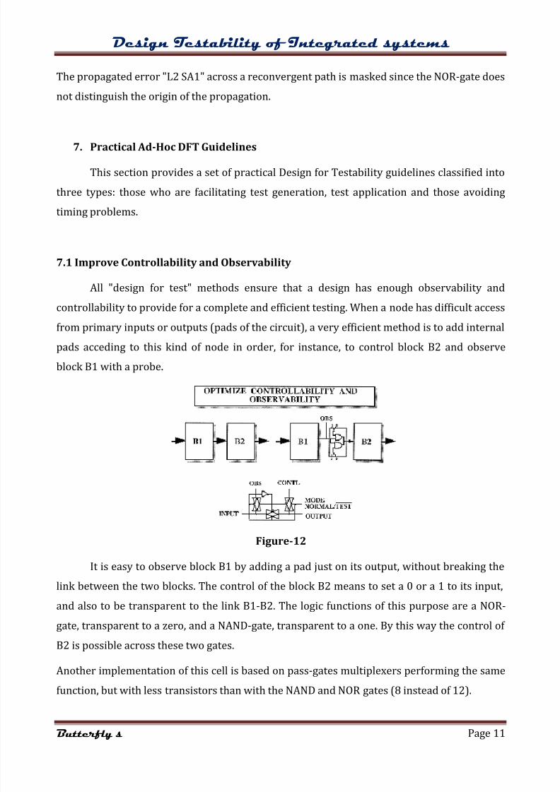
7.1 Improve Controllability and Observability
All "design for test" methods ensure that a design has enough observability and
controllability to provide for a complete and efficient testing. When a node has difficult access
from primary inputs or outputs (pads of the circuit), a very efficient method is to add internal
pads acceding to this kind of node in order, for instance, to control block B2 and observe
block B1 with a probe.
Figure-12
It is easy to observe block B1 by adding a pad just on its output, without breaking the
link between the two blocks. The control of the block B2 means to set a 0 or a 1 to its input,
and also to be transparent to the link B1-B2. The logic functions of this purpose are a NOR-
gate, transparent to a zero, and a NAND-gate, transparent to a one. By this way the control of
B2 is possible across these two gates.
Another implementation of this cell is based on pass-gates multiplexers performing the same
function, but with less transistors than with the NAND and NOR gates (8 instead of 12).
Page 12
8/6/2019 Testability of Integrated Systems
http://slidepdf.com/reader/full/testability-of-integrated-systems 12/24
Design Testability of Integrated systems
Butterfly’ s Page 12
The simple optimization of observation and control is not enough to guarantee a full
testability of the blocks B1 and B2. This technique has to be completed with some other
techniques of testing depending on the internal structures of blocks B1 and B2.
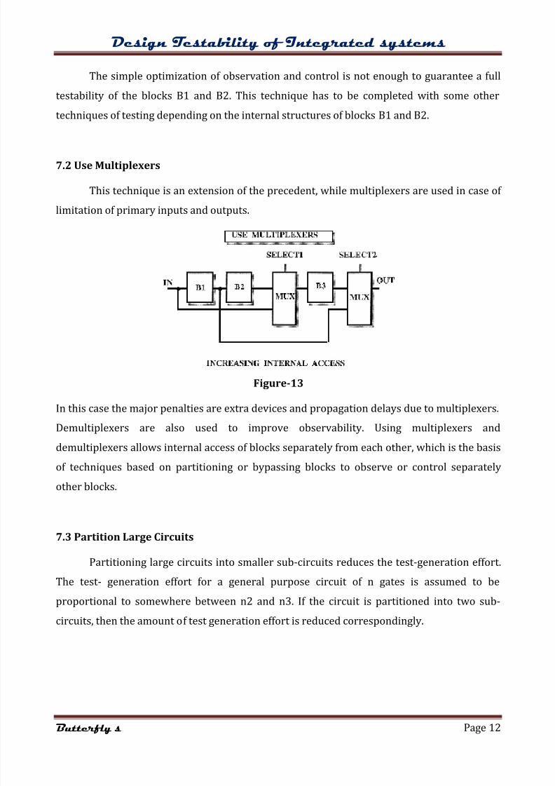
7.2 Use Multiplexers
This technique is an extension of the precedent, while multiplexers are used in case of
limitation of primary inputs and outputs.
Figure-13
In this case the major penalties are extra devices and propagation delays due to multiplexers.Demultiplexers are also used to improve observability. Using multiplexers and
demultiplexers allows internal access of blocks separately from each other, which is the basis
of techniques based on partitioning or bypassing blocks to observe or control separately
other blocks.
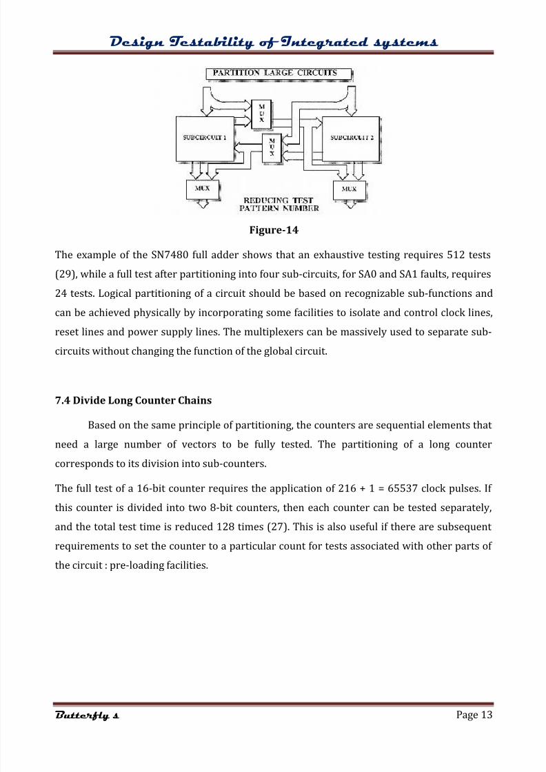
7.3 Partition Large Circuits
Partitioning large circuits into smaller sub-circuits reduces the test-generation effort.
The test- generation effort for a general purpose circuit of n gates is assumed to be
proportional to somewhere between n2 and n3. If the circuit is partitioned into two sub-
circuits, then the amount of test generation effort is reduced correspondingly.
Page 13
8/6/2019 Testability of Integrated Systems
http://slidepdf.com/reader/full/testability-of-integrated-systems 13/24
Design Testability of Integrated systems
Butterfly’ s Page 13
Figure-14
The example of the SN7480 full adder shows that an exhaustive testing requires 512 tests
(29), while a full test after partitioning into four sub-circuits, for SA0 and SA1 faults, requires
24 tests. Logical partitioning of a circuit should be based on recognizable sub-functions and
can be achieved physically by incorporating some facilities to isolate and control clock lines,
reset lines and power supply lines. The multiplexers can be massively used to separate sub-
circuits without changing the function of the global circuit.
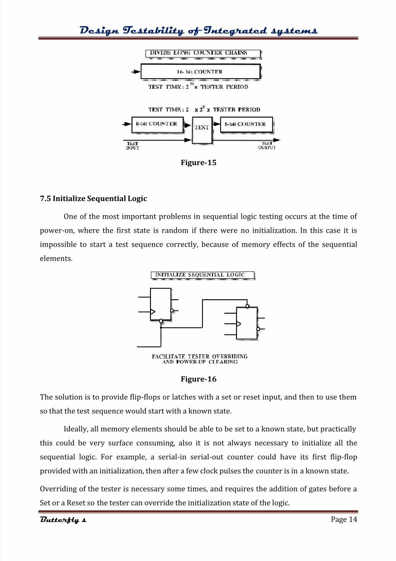
7.4 Divide Long Counter Chains
Based on the same principle of partitioning, the counters are sequential elements that
need a large number of vectors to be fully tested. The partitioning of a long counter
corresponds to its division into sub-counters.
The full test of a 16-bit counter requires the application of 216 + 1 = 65537 clock pulses. If
this counter is divided into two 8-bit counters, then each counter can be tested separately,
and the total test time is reduced 128 times (27). This is also useful if there are subsequent
requirements to set the counter to a particular count for tests associated with other parts of
the circuit : pre-loading facilities.
Page 14
8/6/2019 Testability of Integrated Systems
http://slidepdf.com/reader/full/testability-of-integrated-systems 14/24
Design Testability of Integrated systems
Butterfly’ s Page 14
Figure-15
7.5 Initialize Sequential Logic
One of the most important problems in sequential logic testing occurs at the time of
power-on, where the first state is random if there were no initialization. In this case it is
impossible to start a test sequence correctly, because of memory effects of the sequential
elements.
Figure-16
The solution is to provide flip-flops or latches with a set or reset input, and then to use them
so that the test sequence would start with a known state.
Ideally, all memory elements should be able to be set to a known state, but practically
this could be very surface consuming, also it is not always necessary to initialize all the
sequential logic. For example, a serial-in serial-out counter could have its first flip-flop
provided with an initialization, then after a few clock pulses the counter is in a known state.
Overriding of the tester is necessary some times, and requires the addition of gates before aSet or a Reset so the tester can override the initialization state of the logic.
Page 15
8/6/2019 Testability of Integrated Systems
http://slidepdf.com/reader/full/testability-of-integrated-systems 15/24
Design Testability of Integrated systems
Butterfly’ s Page 15
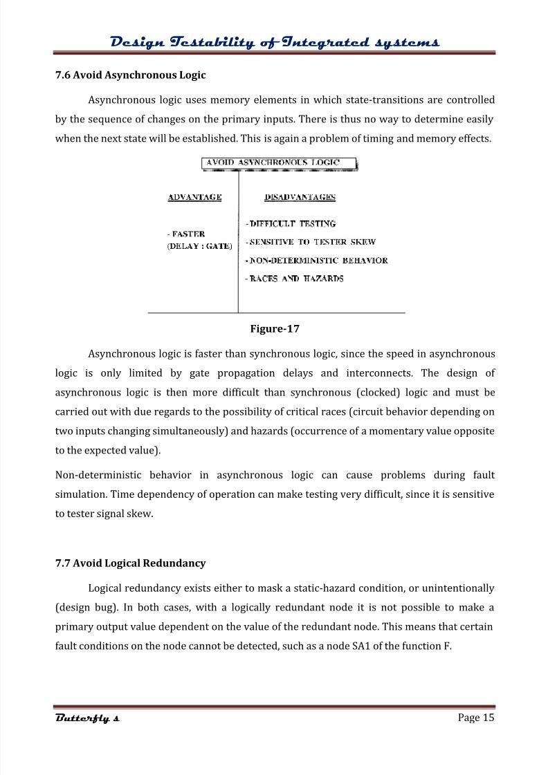
7.6 Avoid Asynchronous Logic
Asynchronous logic uses memory elements in which state-transitions are controlled
by the sequence of changes on the primary inputs. There is thus no way to determine easily
when the next state will be established. This is again a problem of timing and memory effects.
Figure-17
Asynchronous logic is faster than synchronous logic, since the speed in asynchronous
logic is only limited by gate propagation delays and interconnects. The design of
asynchronous logic is then more difficult than synchronous (clocked) logic and must be
carried out with due regards to the possibility of critical races (circuit behavior depending on
two inputs changing simultaneously) and hazards (occurrence of a momentary value opposite
to the expected value).
Non-deterministic behavior in asynchronous logic can cause problems during fault
simulation. Time dependency of operation can make testing very difficult, since it is sensitive
to tester signal skew.
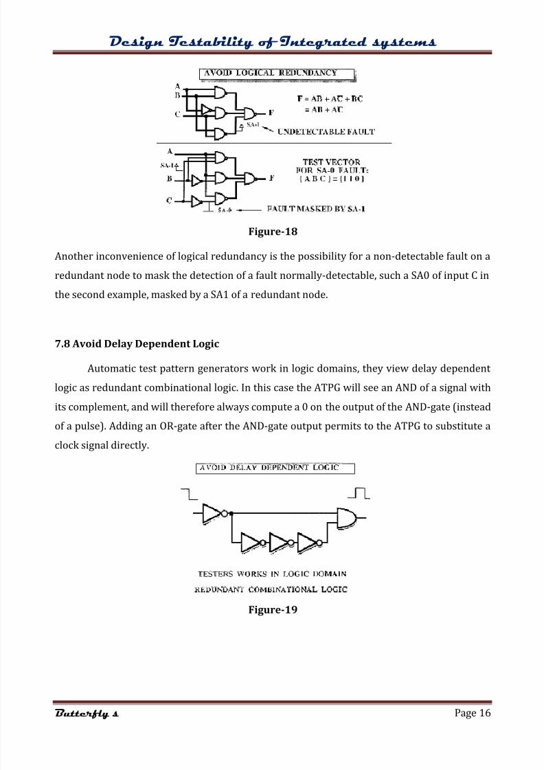
7.7 Avoid Logical Redundancy
Logical redundancy exists either to mask a static-hazard condition, or unintentionally
(design bug). In both cases, with a logically redundant node it is not possible to make a
primary output value dependent on the value of the redundant node. This means that certain
fault conditions on the node cannot be detected, such as a node SA1 of the function F.
Page 16
8/6/2019 Testability of Integrated Systems
http://slidepdf.com/reader/full/testability-of-integrated-systems 16/24
Design Testability of Integrated systems
Butterfly’ s Page 16
Figure-18
Another inconvenience of logical redundancy is the possibility for a non-detectable fault on a
redundant node to mask the detection of a fault normally-detectable, such a SA0 of input C in
the second example, masked by a SA1 of a redundant node.
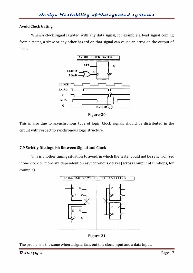
7.8 Avoid Delay Dependent Logic
Automatic test pattern generators work in logic domains, they view delay dependent
logic as redundant combinational logic. In this case the ATPG will see an AND of a signal with
its complement, and will therefore always compute a 0 on the output of the AND-gate (instead
of a pulse). Adding an OR-gate after the AND-gate output permits to the ATPG to substitute a
clock signal directly.
Figure-19
Page 17
8/6/2019 Testability of Integrated Systems
http://slidepdf.com/reader/full/testability-of-integrated-systems 17/24
Design Testability of Integrated systems
Butterfly’ s Page 17
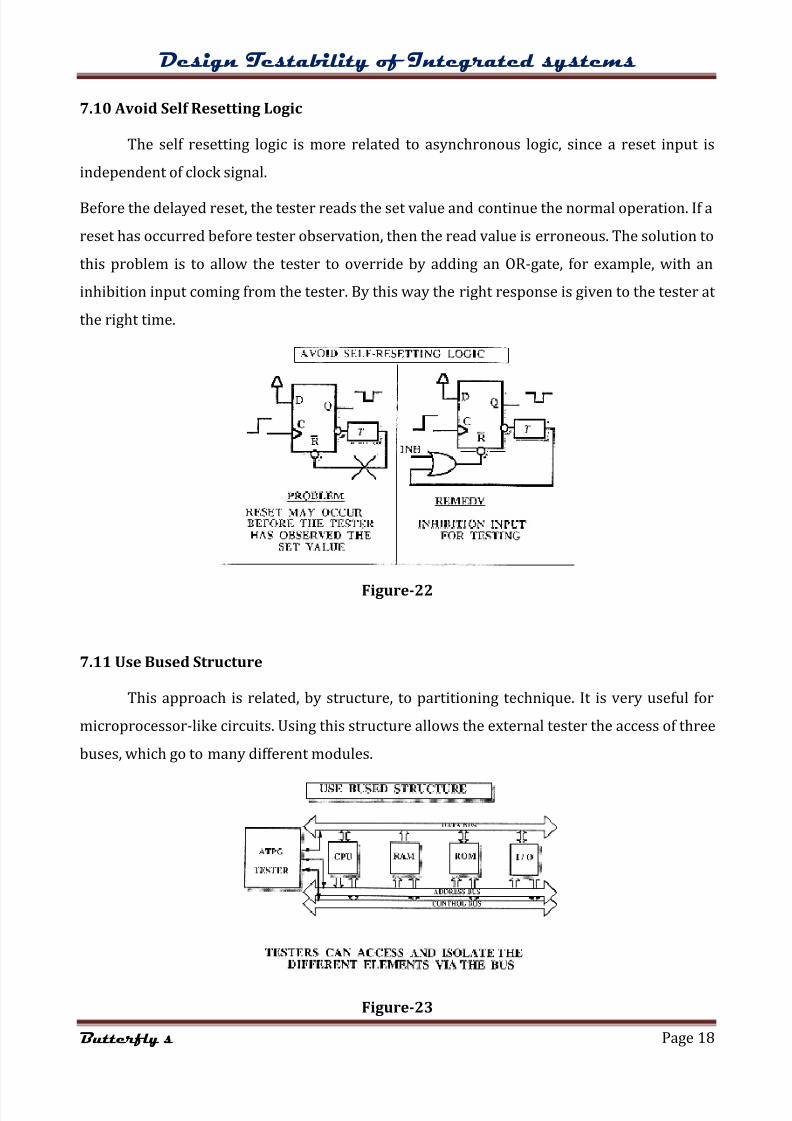
Avoid Clock Gating
When a clock signal is gated with any data signal, for example a load signal coming
from a tester, a skew or any other hazard on that signal can cause an error on the output of
logic.
Figure-20
This is also due to asynchronous type of logic. Clock signals should be distributed in the
circuit with respect to synchronous logic structure.
7.9 Strictly Distinguish Between Signal and Clock
This is another timing situation to avoid, in which the tester could not be synchronized
if one clock or more are dependent on asynchronous delays (across D-input of flip-flops, for
example).
Figure-21
The problem is the same when a signal fans out to a clock input and a data input.
Page 18
8/6/2019 Testability of Integrated Systems
http://slidepdf.com/reader/full/testability-of-integrated-systems 18/24
Design Testability of Integrated systems
Butterfly’ s Page 18
7.10 Avoid Self Resetting Logic
The self resetting logic is more related to asynchronous logic, since a reset input is
independent of clock signal.
Before the delayed reset, the tester reads the set value and continue the normal operation. If a
reset has occurred before tester observation, then the read value is erroneous. The solution to
this problem is to allow the tester to override by adding an OR-gate, for example, with an
inhibition input coming from the tester. By this way the right response is given to the tester at
the right time.
Figure-22
7.11 Use Bused Structure
This approach is related, by structure, to partitioning technique. It is very useful for
microprocessor-like circuits. Using this structure allows the external tester the access of three
buses, which go to many different modules.
Figure-23
Page 19
8/6/2019 Testability of Integrated Systems
http://slidepdf.com/reader/full/testability-of-integrated-systems 19/24
Design Testability of Integrated systems
Butterfly’ s Page 19
The tester can then disconnect any module from the buses by putting its output into a high-
impedance state. Test patterns can then be applied to each module separately.
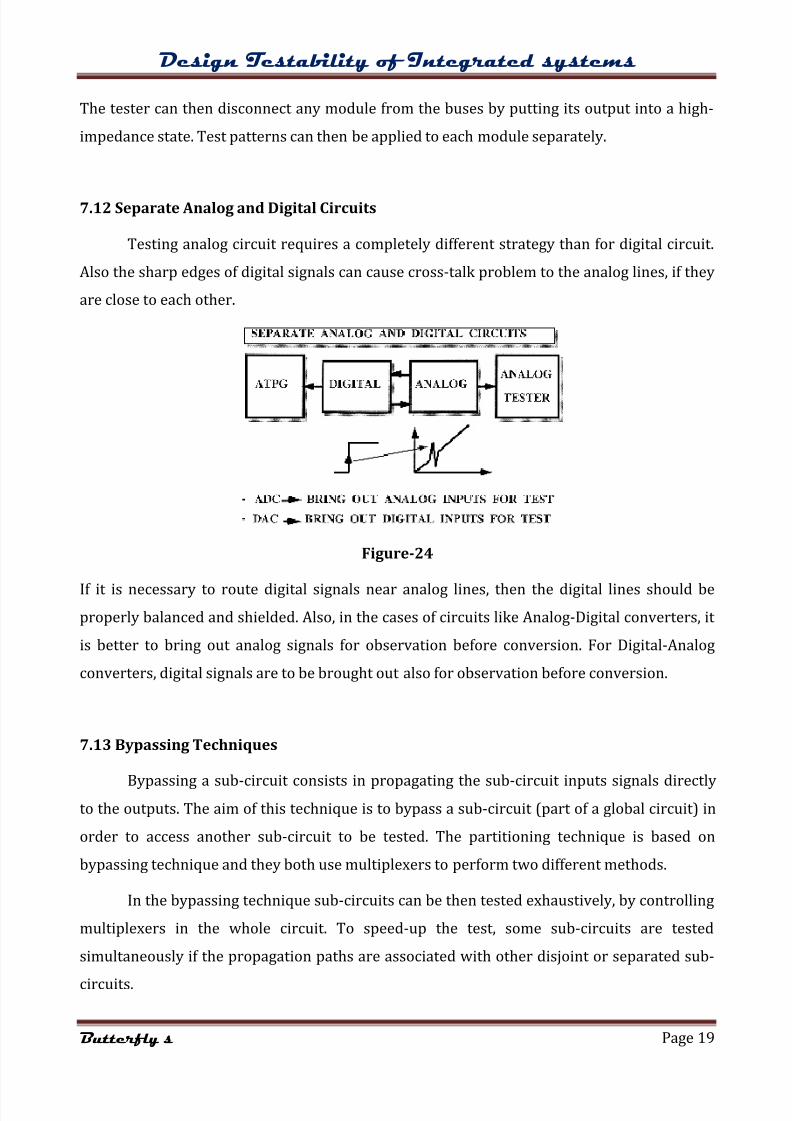
7.12 Separate Analog and Digital Circuits
Testing analog circuit requires a completely different strategy than for digital circuit.
Also the sharp edges of digital signals can cause cross-talk problem to the analog lines, if they
are close to each other.
Figure-24
If it is necessary to route digital signals near analog lines, then the digital lines should be
properly balanced and shielded. Also, in the cases of circuits like Analog-Digital converters, it
is better to bring out analog signals for observation before conversion. For Digital-Analog
converters, digital signals are to be brought out also for observation before conversion.
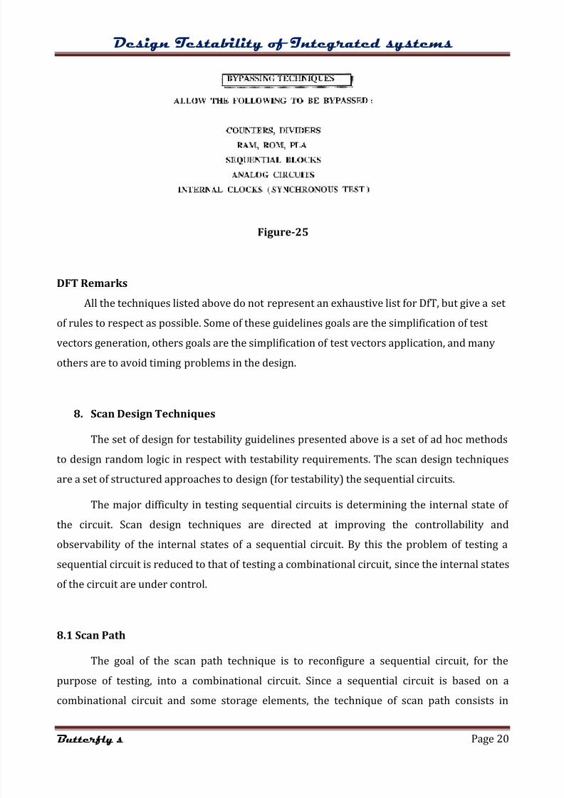
7.13 Bypassing Techniques
Bypassing a sub-circuit consists in propagating the sub-circuit inputs signals directlyto the outputs. The aim of this technique is to bypass a sub-circuit (part of a global circuit) in
order to access another sub-circuit to be tested. The partitioning technique is based on
bypassing technique and they both use multiplexers to perform two different methods.
In the bypassing technique sub-circuits can be then tested exhaustively, by controlling
multiplexers in the whole circuit. To speed-up the test, some sub-circuits are tested
simultaneously if the propagation paths are associated with other disjoint or separated sub-
circuits.
Page 20
8/6/2019 Testability of Integrated Systems
http://slidepdf.com/reader/full/testability-of-integrated-systems 20/24
Design Testability of Integrated systems
Butterfly’ s Page 20
Figure-25
DFT Remarks
All the techniques listed above do not represent an exhaustive list for DfT, but give a set
of rules to respect as possible. Some of these guidelines goals are the simplification of test
vectors generation, others goals are the simplification of test vectors application, and many
others are to avoid timing problems in the design.
8. Scan Design Techniques
The set of design for testability guidelines presented above is a set of ad hoc methods
to design random logic in respect with testability requirements. The scan design techniques
are a set of structured approaches to design (for testability) the sequential circuits.
The major difficulty in testing sequential circuits is determining the internal state of
the circuit. Scan design techniques are directed at improving the controllability and
observability of the internal states of a sequential circuit. By this the problem of testing a
sequential circuit is reduced to that of testing a combinational circuit, since the internal states
of the circuit are under control.
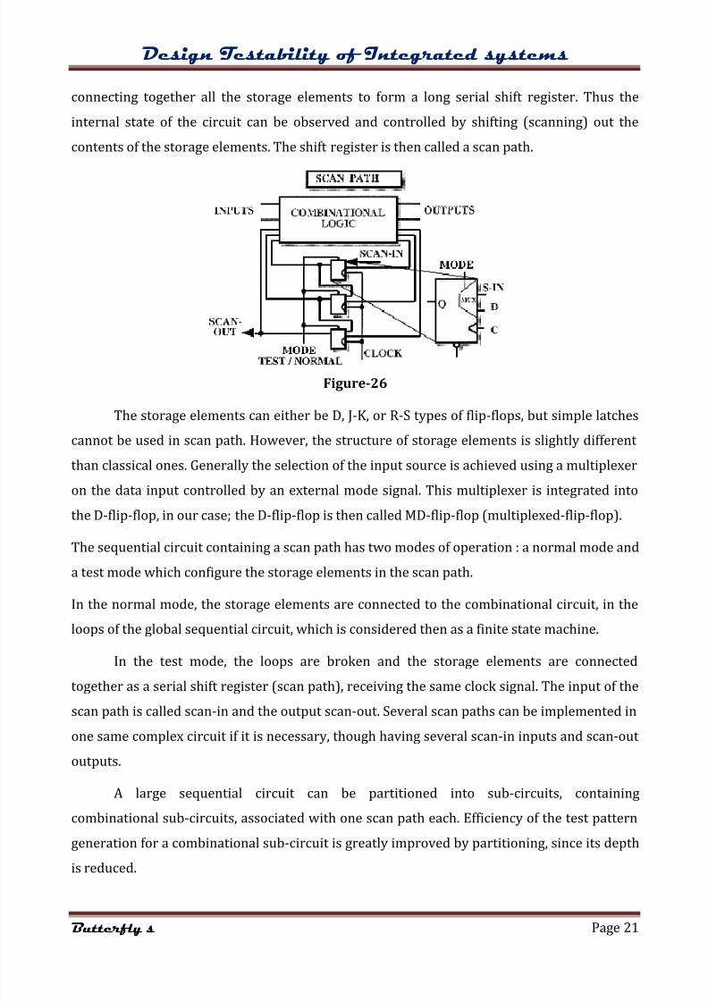
8.1 Scan Path
The goal of the scan path technique is to reconfigure a sequential circuit, for the
purpose of testing, into a combinational circuit. Since a sequential circuit is based on a
combinational circuit and some storage elements, the technique of scan path consists in
Page 21
8/6/2019 Testability of Integrated Systems
http://slidepdf.com/reader/full/testability-of-integrated-systems 21/24
Design Testability of Integrated systems
Butterfly’ s Page 21
connecting together all the storage elements to form a long serial shift register. Thus the
internal state of the circuit can be observed and controlled by shifting (scanning) out the
contents of the storage elements. The shift register is then called a scan path.
Figure-26
The storage elements can either be D, J-K, or R-S types of flip-flops, but simple latches
cannot be used in scan path. However, the structure of storage elements is slightly different
than classical ones. Generally the selection of the input source is achieved using a multiplexer
on the data input controlled by an external mode signal. This multiplexer is integrated into
the D-flip-flop, in our case; the D-flip-flop is then called MD-flip-flop (multiplexed-flip-flop).
The sequential circuit containing a scan path has two modes of operation : a normal mode and
a test mode which configure the storage elements in the scan path.
In the normal mode, the storage elements are connected to the combinational circuit, in the
loops of the global sequential circuit, which is considered then as a finite state machine.
In the test mode, the loops are broken and the storage elements are connected
together as a serial shift register (scan path), receiving the same clock signal. The input of the
scan path is called scan-in and the output scan-out. Several scan paths can be implemented in
one same complex circuit if it is necessary, though having several scan-in inputs and scan-out
outputs.
A large sequential circuit can be partitioned into sub-circuits, containing
combinational sub-circuits, associated with one scan path each. Efficiency of the test pattern
generation for a combinational sub-circuit is greatly improved by partitioning, since its depth
is reduced.
Page 22
8/6/2019 Testability of Integrated Systems
http://slidepdf.com/reader/full/testability-of-integrated-systems 22/24
Design Testability of Integrated systems
Butterfly’ s Page 22
Before applying test patterns, the shift register itself has to be verified by shifting in all ones
i.e. 111...11, or zeros i.e. 000...00, and comparing.
The method of testing a circuit with the scan path is as follows:
1. Set test mode signal, flip-flops accept data from input scan-in
2. Verify the scan path by shifting in and out test data
3. Set the shift register to an initial state
4. Apply a test pattern to the primary inputs of the circuit
5. Set normal mode, the circuit settles and can monitor the primary outputs of the circuit
6.
Activate the circuit clock for one cycle
7. Return to test mode
8. Scan out the contents of the registers, simultaneously scan in the next pattern
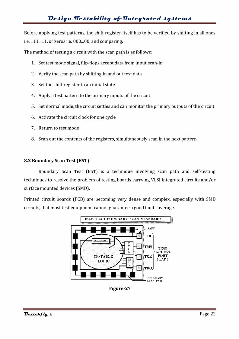
8.2 Boundary Scan Test (BST)
Boundary Scan Test (BST) is a technique involving scan path and self-testing
techniques to resolve the problem of testing boards carrying VLSI integrated circuits and/or
surface mounted devices (SMD).
Printed circuit boards (PCB) are becoming very dense and complex, especially with SMD
circuits, that most test equipment cannot guarantee a good fault coverage.
Figure-27
Page 23
8/6/2019 Testability of Integrated Systems
http://slidepdf.com/reader/full/testability-of-integrated-systems 23/24
Design Testability of Integrated systems
Butterfly’ s Page 23
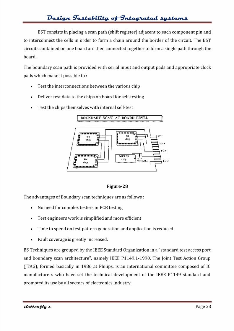
BST consists in placing a scan path (shift register) adjacent to each component pin and
to interconnect the cells in order to form a chain around the border of the circuit. The BST
circuits contained on one board are then connected together to form a single path through the
board.
The boundary scan path is provided with serial input and output pads and appropriate clock
pads which make it possible to :
Test the interconnections between the various chip
Deliver test data to the chips on board for self-testing
Test the chips themselves with internal self-test
Figure-28
The advantages of Boundary scan techniques are as follows :
No need for complex testers in PCB testing
Test engineers work is simplified and more efficient
Time to spend on test pattern generation and application is reduced
Fault coverage is greatly increased.
BS Techniques are grouped by the IEEE Standard Organization in a "standard test access port
and boundary scan architecture", namely IEEE P1149.1-1990. The Joint Test Action Group
(JTAG), formed basically in 1986 at Philips, is an international committee composed of IC
manufacturers who have set the technical development of the IEEE P1149 standard and
promoted its use by all sectors of electronics industry.
Page 24
8/6/2019 Testability of Integrated Systems
http://slidepdf.com/reader/full/testability-of-integrated-systems 24/24
Design Testability of Integrated systems
B fl ’ P 24
The IEEE 1149 is a family of overall testability bus standards, defined by the Joint Test Action
Group (JTAG), formed basically in 1986 at Philips. JTAG is an international committee
composed of European and American IC manufacturers. The "standard Test Access Port and
Boundary Scan architecture", namely IEEE P1149.1 accepted by the IEEE standard committeein February1990, is the first one of this family. Several other ongoing standards are developed
and suggested as drafts to the technical committee of the IEEE 1149 standard in order to
promote their use by all sectors of electronics industry.