Page 1
© February 7, 2013 Dr. Lynn Fuller
Testing – Device Problem Analysis
Page 1
Rochester Institute of Technology
Microelectronic Engineering
ROCHESTER INSTITUTE OF TECHNOLOGYMICROELECTRONIC ENGINEERING
Testing – Device Problem Analysis
Dr. Lynn FullerWebpage: http://people.rit.edu/lffeee
Microelectronic EngineeringRochester Institute of Technology
82 Lomb Memorial DriveRochester, NY 14623-5604
Tel (585) 475-2035Fax (585) 475-5041
Email: [email protected] webpage: http://www.microe.rit.edu
2-7-2013 Testing-Device-Problem-Analysis.ppt
Page 2
© February 7, 2013 Dr. Lynn Fuller
Testing – Device Problem Analysis
Page 2
Rochester Institute of Technology
Microelectronic Engineering
OUTLINE
IntroductionGood Device CharacteristicsVarious Not So Good Device CharacteristicsDiscussion of CharacteristicsDesign Errors Fabrication Problems
Page 3
© February 7, 2013 Dr. Lynn Fuller
Testing – Device Problem Analysis
Page 3
Rochester Institute of Technology
Microelectronic Engineering
INTRODUCTION
This document is a collection of test results showing problems with various semiconductor devices made in the microelectronics fabrication laboratory. The objective is to provide useful information for identification of the source of problems and to enhance the education of our students.
Page 4
© February 7, 2013 Dr. Lynn Fuller
Testing – Device Problem Analysis
Page 4
Rochester Institute of Technology
Microelectronic Engineering
GOOD NMOS DEVICE CHARACTERISTICS
Page 5
© February 7, 2013 Dr. Lynn Fuller
Testing – Device Problem Analysis
Page 5
Rochester Institute of Technology
Microelectronic Engineering
GOOD PMOS DEVICE CHARACTERISTICS
Page 6
© February 7, 2013 Dr. Lynn Fuller
Testing – Device Problem Analysis
Page 6
Rochester Institute of Technology
Microelectronic Engineering
NON OHMIC CONTACT TO NMOS DRAIN/SOURCE IN SUB-CMOS PROCESS
Page 7
© February 7, 2013 Dr. Lynn Fuller
Testing – Device Problem Analysis
Page 7
Rochester Institute of Technology
Microelectronic Engineering
NON OHMIC CONTACT TO NMOS DRAIN/SOURCE IN SUB-CMOS PROCESS
N-N+
Over etched contact cuts makes a non-ohmic (rectifying or Schottky) contact with the lighter doped n-type area of the drain/source. P-type devices have ohmic contacts.
< 1um
Page 8
© February 7, 2013 Dr. Lynn Fuller
Testing – Device Problem Analysis
Page 8
Rochester Institute of Technology
Microelectronic Engineering
CONTACTS TO SILICON
Ideal OhmicAl/p-silicon
Tunneling OhmicAl/n+-silicon
RectifyingAl/n-silicon
V
I
V
I
V
I
Page 9
© February 7, 2013 Dr. Lynn Fuller
Testing – Device Problem Analysis
Page 9
Rochester Institute of Technology
Microelectronic Engineering
NON OHMIC CONTACT TO NMOS DRAIN/SOURCE IN ADV-CMOS PROCESS
0
20
40
60
80
100
120
140
0 1 2 3 4
VD (volts)
ID (
µA
/um
)
VG=3.5V
VG=2.92V
VG=2.33V
VG=1.75V
VG=1.17V
VG=0.58V
Lmask drawn = 0.6 µm
Leffective = 0.4 µm
*This is RIT’s first sub-0.5 µm Transistor*
Gate
Source Drain
ID-VD for NMOS Transistor
Mike Aquilino May 2004
Page 10
© February 7, 2013 Dr. Lynn Fuller
Testing – Device Problem Analysis
Page 10
Rochester Institute of Technology
Microelectronic Engineering
SILICIDE FORMATION CONSUMES SILICON
N+< 1um
IMEC MeetingDecember 1999
Too much silicide formation makes a non-ohmic (rectifying or Schottky) contact with the lighter doped n-type area of the drain/source.
TiSi2
N-
Page 11
© February 7, 2013 Dr. Lynn Fuller
Testing – Device Problem Analysis
Page 11
Rochester Institute of Technology
Microelectronic Engineering
EFFECT OF SINTER ON IV CHARACTERISTICS
Native Oxide
Before Sinter After Sinter
Page 12
© February 7, 2013 Dr. Lynn Fuller
Testing – Device Problem Analysis
Page 12
Rochester Institute of Technology
Microelectronic Engineering
DIFFERENT LOOKING FAMILY OF CURVES AT DIFFERENT LOCATIONS ON THE WAFER
2µm/32µm L/W NMOS AND PMOS
Family of curves for L=2µm MOSFETs
Page 13
© February 7, 2013 Dr. Lynn Fuller
Testing – Device Problem Analysis
Page 13
Rochester Institute of Technology
Microelectronic Engineering
NON UNIFORMITY IN PLASMA ETCH OF POLY
2µm/32µm L/W NMOS AND PMOS
Family of curves for L=2µm MOSFETs
Page 14
© February 7, 2013 Dr. Lynn Fuller
Testing – Device Problem Analysis
Page 14
Rochester Institute of Technology
Microelectronic Engineering
GOOD DEVICE SUB THRESHOLD CHARACTERISTICS
Occasionally our 1um Devices WorkWhy does the sub-threshold plot not flatten out at the bottom?
Answer: Vt is ~0.5 volt and swing is ~100mV/decade so at zero voltsthe device can be down 5 decades of current which is 10-10 it should flatten out at ~ 10-11 or 10-12 …… need higher Vt or smaller swing
Page 15
© February 7, 2013 Dr. Lynn Fuller
Testing – Device Problem Analysis
Page 15
Rochester Institute of Technology
Microelectronic Engineering
SHORT CHANNEL – BAD SUB THESHOLD
Page 16
© February 7, 2013 Dr. Lynn Fuller
Testing – Device Problem Analysis
Page 16
Rochester Institute of Technology
Microelectronic Engineering
REALLY SHORT CHANNEL
Page 17
© February 7, 2013 Dr. Lynn Fuller
Testing – Device Problem Analysis
Page 17
Rochester Institute of Technology
Microelectronic Engineering
DRAIN INDUCED BARRIER LOWERING
DIBL = change in VG /change in VDat ID=1E-9 amps/µmor 1.6E-8 amps for thissize transistor
= ~ (1.1957-1.1463)/(5-0.1)= ~ 10mV/V
L/W=2/16
Page 18
© February 7, 2013 Dr. Lynn Fuller
Testing – Device Problem Analysis
Page 18
Rochester Institute of Technology
Microelectronic Engineering
PUNCH THROUGH
Page 19
© February 7, 2013 Dr. Lynn Fuller
Testing – Device Problem Analysis
Page 19
Rochester Institute of Technology
Microelectronic Engineering
MOBILITY DEGRADATION
32/16
Page 20
© February 7, 2013 Dr. Lynn Fuller
Testing – Device Problem Analysis
Page 20
Rochester Institute of Technology
Microelectronic Engineering
VELOCITY SATURATION
Page 21
© February 7, 2013 Dr. Lynn Fuller
Testing – Device Problem Analysis
Page 21
Rochester Institute of Technology
Microelectronic Engineering
RIT’s FIRST SUB MICRON TRANSISTOR
Mark Klare 7/22/94 Electron beam direct write on wafer, n-well process 5E12 dose, P+ Poly Gate PMOS, shallow BF2 D/S implant, no Vt adjust implant.
L=0.75 umXox=300 ÅD/S Xj = 0.25 µmP+ polyNd well ~3E16
Vt = -0.15Sub Vt Slope=130 mV/dec
-3.0-2.5-2.0-1.5-1.0-0.5
0 3.0Vds VoltsId
s (m
A)
0
-8
Page 22
© February 7, 2013 Dr. Lynn Fuller
Testing – Device Problem Analysis
Page 22
Rochester Institute of Technology
Microelectronic Engineering
WHAT IS WRONG?
NO CONNECTION
Switch Matrix Programmed WrongSwitch Matrix Not CopiedIncomplete Contact Cut EtchAluminum Oxide Between M1 and M2
Page 23
© February 7, 2013 Dr. Lynn Fuller
Testing – Device Problem Analysis
Page 23
Rochester Institute of Technology
Microelectronic Engineering
GOOD RESISTOR CHARACTERISTICS
Page 24
© February 7, 2013 Dr. Lynn Fuller
Testing – Device Problem Analysis
Page 24
Rochester Institute of Technology
Microelectronic Engineering
IS THIS GOOD?
NO
Open Circuit, both electrical and visual evidence
Page 25
© February 7, 2013 Dr. Lynn Fuller
Testing – Device Problem Analysis
Page 25
Rochester Institute of Technology
Microelectronic Engineering
IS THIS GOOD?
NO
R = 1/ slope = 1/.03357m = 29,788 ohmswhich is 58 ohms/contact512 Vias
Page 26
© February 7, 2013 Dr. Lynn Fuller
Testing – Device Problem Analysis
Page 26
Rochester Institute of Technology
Microelectronic Engineering
IS THIS GOOD?
F081201
YESM1-M2 Via chain with 512 Vias and total resistance of 118 ohms or 0.231 ohms per contact
512 Vias
Page 27
© February 7, 2013 Dr. Lynn Fuller
Testing – Device Problem Analysis
Page 27
Rochester Institute of Technology
Microelectronic Engineering
WHAT IS WRONG?
Testing PMOS with NMOS-1 Setup Testing PMOS with PMOS-1 Setup
Page 28
© February 7, 2013 Dr. Lynn Fuller
Testing – Device Problem Analysis
Page 28
Rochester Institute of Technology
Microelectronic Engineering
WHAT IS WRONG?
Leff is almost zero
Poly over etched making L too smallPMOS works at L/W = 2/4 but not at 1/4
Page 29
© February 7, 2013 Dr. Lynn Fuller
Testing – Device Problem Analysis
Page 29
Rochester Institute of Technology
Microelectronic Engineering
NON UNIFORMITY IN PLASMA ETCH OF POLY
2µm/32µm L/W NMOS AND PMOS
Family of curves for L=2µm MOSFETs
Lot Number = F050118 Wafer Number = D3
Page 30
© February 7, 2013 Dr. Lynn Fuller
Testing – Device Problem Analysis
Page 30
Rochester Institute of Technology
Microelectronic Engineering
SINGLE AND DUAL PHOTO CELL
Isc = 0.585 uAor 3.25 A/m2
Isc = 1.088 uAor 6 A/m2
Diode CharacteristicsShifts Down with Light
Page 31
© February 7, 2013 Dr. Lynn Fuller
Testing – Device Problem Analysis
Page 31
Rochester Institute of Technology
Microelectronic Engineering
8-CELL PHOTO BATTERY – NOT CORRECT
Design ErrorsN-Wells too closeN+ and P+ not correct
Page 32
© February 7, 2013 Dr. Lynn Fuller
Testing – Device Problem Analysis
Page 32
Rochester Institute of Technology
Microelectronic Engineering
8-CELL PHOTO BATTERY
Design Errors FixedDiode CharacteristicsShifts Down with Light
Page 33
© February 7, 2013 Dr. Lynn Fuller
Testing – Device Problem Analysis
Page 33
Rochester Institute of Technology
Microelectronic Engineering
WHAT IS WRONG WITH THIS DIGITAL CIRCUIT
Design Errors – Missing Contact Cuts
Page 34
© February 7, 2013 Dr. Lynn Fuller
Testing – Device Problem Analysis
Page 34
Rochester Institute of Technology
Microelectronic Engineering
MASK DEFECTS
Page 35
© February 7, 2013 Dr. Lynn Fuller
Testing – Device Problem Analysis
Page 35
Rochester Institute of Technology
Microelectronic Engineering
JOHN GALT CMOS TESTCHIP
2010
Defect
Page 36
© February 7, 2013 Dr. Lynn Fuller
Testing – Device Problem Analysis
Page 36
Rochester Institute of Technology
Microelectronic Engineering
MASK DEFECT
160 um
100 um
Defect
This defect will cause a short through the pn junction of our solar cell.
Chrome Side of
N-well Mask
Page 37
© February 7, 2013 Dr. Lynn Fuller
Testing – Device Problem Analysis
Page 37
Rochester Institute of Technology
Microelectronic Engineering
LARGE 5mm X 5mm PHOTODIODE
Isc = 0.15mA (short circuit current)or 9.09 A/m2
5mmx
3.33mm
Page 38
© February 7, 2013 Dr. Lynn Fuller
Testing – Device Problem Analysis
Page 38
Rochester Institute of Technology
Microelectronic Engineering
73 STAGE RING OSCILLATOR
73 Stage4X Buffer
L=2µm5Volt Supply
Frequency = 4.37MHzPeriod = T = 2 N td = 230ns
td = 1.58ns
Design Photo
Electrical Test Results
The Ring Oscillator WorksIs It Working Correctly?
Page 39
© February 7, 2013 Dr. Lynn Fuller
Testing – Device Problem Analysis
Page 39
Rochester Institute of Technology
Microelectronic Engineering
RING OSCILLATOR LAYOUTS
17 Stage Un-buffered Output
L/W 8/16 4/16 2/16
L/W=2/30 Buffered Output
73 Stage 37 Stage
Page 40
© February 7, 2013 Dr. Lynn Fuller
Testing – Device Problem Analysis
Page 40
Rochester Institute of Technology
Microelectronic Engineering
MOSFETS IN THE INVERTER OF 73 RING OSCILLATOR
nmosfet pmosfet
73 Stage Ring Oscillator
Page 41
© February 7, 2013 Dr. Lynn Fuller
Testing – Device Problem Analysis
Page 41
Rochester Institute of Technology
Microelectronic Engineering
FIND DIMENSIONS OF THE TRANSISTORS
NMOS PMOS
L 2u 2u
W 12u 30u
AD 12ux12u=144p 12ux30u=360p
AS 12ux12u=144p 12ux30u=360p
PD 2x(12u+12u)=48u 2x(12u+30u)=84u
PS 2x(12u+12u)=48u 2x(12u+30u)=84u
NRS 1 0.3
NRD 1 0.3
Use Ctrl Click on all NMOS on OrCad SchematicUse Ctrl Click on all PMOS on OrCad SchematicThen Enter Dimensions
73 Stage
Page 42
© February 7, 2013 Dr. Lynn Fuller
Testing – Device Problem Analysis
Page 42
Rochester Institute of Technology
Microelectronic Engineering
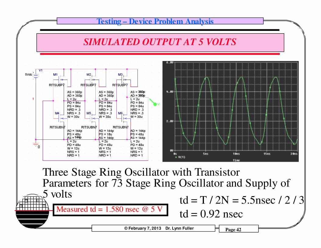
SIMULATED OUTPUT AT 5 VOLTS
Three Stage Ring Oscillator with Transistor Parameters for 73 Stage Ring Oscillator and Supply of 5 volts td = T / 2N = 5.5nsec / 2 / 3
td = 0.92 nsecMeasured td = 1.580 nsec @ 5 V
360p360p
144p
Page 43
© February 7, 2013 Dr. Lynn Fuller
Testing – Device Problem Analysis
Page 43
Rochester Institute of Technology
Microelectronic Engineering
REFERENCES
1. Dr Fuller’s webpage on CMOS testing, http://people.rit.edu/lffeee/CMOS.htm
2. other
Page 44
© February 7, 2013 Dr. Lynn Fuller
Testing – Device Problem Analysis
Page 44
Rochester Institute of Technology
Microelectronic Engineering
HOMEWORK
1. Problem 12. other