An effective ppt to study test proceess and economics
49
VLSI Test: Lecture 2 1 Lecture 2 VLSI Test Process and Equipment Motivation Types of Testing Test Specifications and Plan Test Programming Test Data Analysis Automatic Test Equipment Parametric Testing Summary
Transcript
VLSI Test: Lecture 2 1
Lecture 2VLSI Test Process and
Equipment
Lecture 2VLSI Test Process and
Equipment Motivation
Types of Testing
Test Specifications and Plan
Test Programming
Test Data Analysis
Automatic Test Equipment
Parametric Testing
Summary
VLSI Test: Lecture 2 2
MotivationMotivation
Need to understand Automatic Test Equipment (ATE) technology Influences what tests are possible Serious analog measurement limitations at high
digital frequency or in the analog domain Understand capabilities for digital logic, memory,
and analog test for testing System-on-a-Chip (SOC)
Need to understand parametric testing For setup and hold time measurements For determination of VIL , VIH , VOL , VOH , tr , tf , td , IOL,
IOH , IIL, IIH
VLSI Test: Lecture 2 3
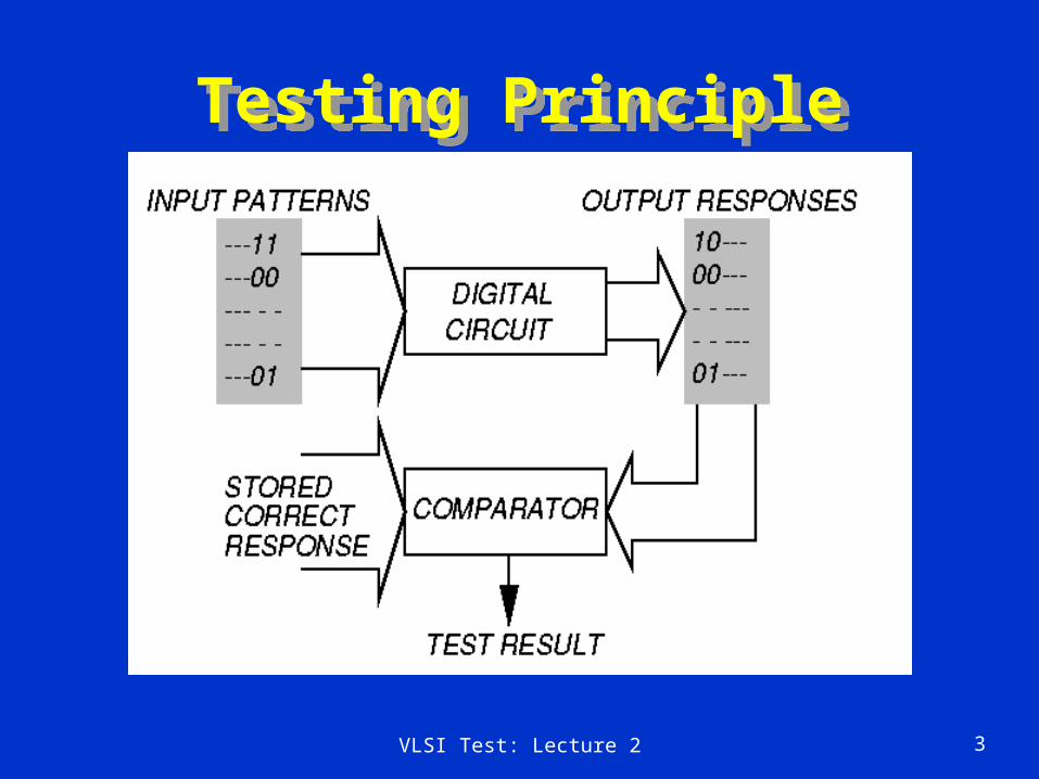
Testing PrincipleTesting Principle
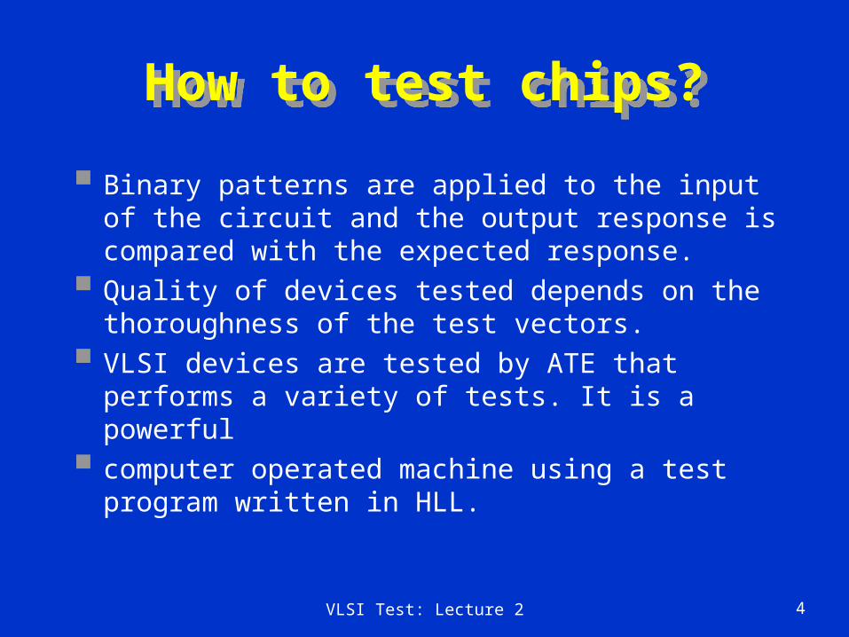
How to test chips?How to test chips?
Binary patterns are applied to the input of the circuit and the output response is compared with the expected response.
Quality of devices tested depends on the thoroughness of the test vectors.
VLSI devices are tested by ATE that performs a variety of tests. It is a powerful
computer operated machine using a test program written in HLL.
VLSI Test: Lecture 2 4
VLSI Test: Lecture 2 5
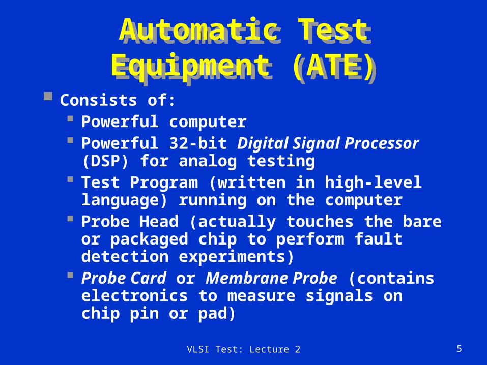
Automatic Test Equipment (ATE)Automatic Test
Equipment (ATE) Consists of:
Powerful computer Powerful 32-bit Digital Signal Processor (DSP)
for analog testing Test Program (written in high-level language)
running on the computer Probe Head (actually touches the bare or
packaged chip to perform fault detection experiments)
Probe Card or Membrane Probe (contains electronics to measure signals on chip pin or pad)
VLSI Test: Lecture 2 6
Characterization or Verification Test
Characterization or Verification Test
Ferociously expensive Applied to selected (not all) parts Used prior to production or manufacturing test
May comprise: Scanning Electron Microscope tests Bright-Lite detection of defects Electron beam testing Artificial intelligence (expert system) methods Repeated functional tests
Test at rated speed or at maximum speed guaranteed by supplier
VLSI Test: Lecture 2 8
Burn-in or Stress TestBurn-in or Stress Test
Process: Subject chips to high temperature and over-
voltage supply, while running production tests
Catches: Infant mortality cases – these are damaged or
weak (low reliability) chips that will fail in the first few days of operation – burn-in causes bad devices to fail before they are shipped to customers
Freak failures – devices having same failure mechanisms as reliable devices
VLSI Test: Lecture 2 9
Incoming InspectionIncoming Inspection
Can be: Similar to production testing More comprehensive than production testing Tuned to specific system application
Often done for a random sample of devices Sample size depends on device quality and
system reliability requirements Avoids putting defective device in a system
where cost of diagnosis and repair exceeds incoming inspection cost
VLSI Test: Lecture 2 10
Manufacturing Test Scenarios
Manufacturing Test Scenarios
Wafer sort or probe test – done before wafer is scribed and cut into chips Includes test site characterization – specific
test devices are checked with specific patterns to measure:
Gate threshold Polysilicon field threshold Poly sheet resistance, etc.
Packaged device tests
VLSI Test: Lecture 2 11
Types of TestsTypes of Tests
Parametric – measures electrical properties of pin electronics – delay, voltages, currents, etc. – fast and cheap
Functional – used to cover very high % of modeled faults – test every transistor and wire in digital circuits – long and expensive – main topic of tutorial
VLSI Test: Lecture 2 12
Two Different Meanings of Functional Test
Two Different Meanings of Functional Test
ATE and Manufacturing World – any vectors applied to cover high % of faults during manufacturing test
Automatic Test-Pattern Generation World – testing with verification vectors, which determine whether hardware matches its specification – typically have low fault coverage (< 70 %)
VLSI Test: Lecture 2 13
Test ProgrammingTest Programming
VLSI Test: Lecture 2 14
Test Data AnalysisTest Data Analysis
Uses of ATE test data: Reject bad DUTs Fabrication process information Design weakness information
Devices that did not fail are good only if tests covered 100% of faults
Failure mode analysis (FMA): Diagnose reasons for device failure, and find
design and process weaknesses Improve logic and layout design rules
VLSI Test: Lecture 2 15
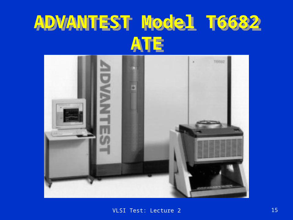
ADVANTEST Model T6682 ATE
ADVANTEST Model T6682 ATE
VLSI Test: Lecture 2 16
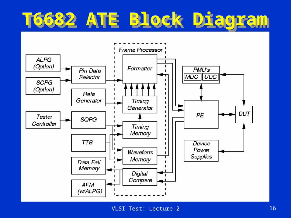
T6682 ATE Block Diagram
T6682 ATE Block Diagram
VLSI Test: Lecture 2 17
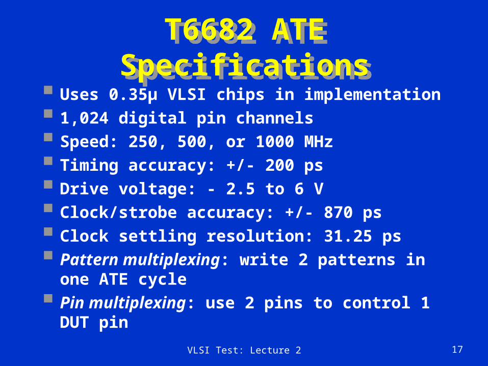
T6682 ATE Specifications
T6682 ATE Specifications
Uses 0.35μ VLSI chips in implementation
1,024 digital pin channels
Speed: 250, 500, or 1000 MHz
Timing accuracy: +/- 200 ps
Drive voltage: - 2.5 to 6 V
Clock/strobe accuracy: +/- 870 ps
Clock settling resolution: 31.25 ps
Pattern multiplexing: write 2 patterns in one ATE cycle
Mvectors of patterns to apply to DUT -- vector width determined by # DUT pins
Algorithmic pattern generator (ALPG): 32 independent address bits, 36 data bits For memory test – has address descrambler Has address failure memory
Scan pattern generator (SCPG) supports JTAG boundary scan, greatly reduces test vector memory for full-scan testing 2 Gvector or 8 Gvector sizes
VLSI Test: Lecture 2 19
Electrical Parametric Testing
Electrical Parametric Testing
VLSI Test: Lecture 2 20
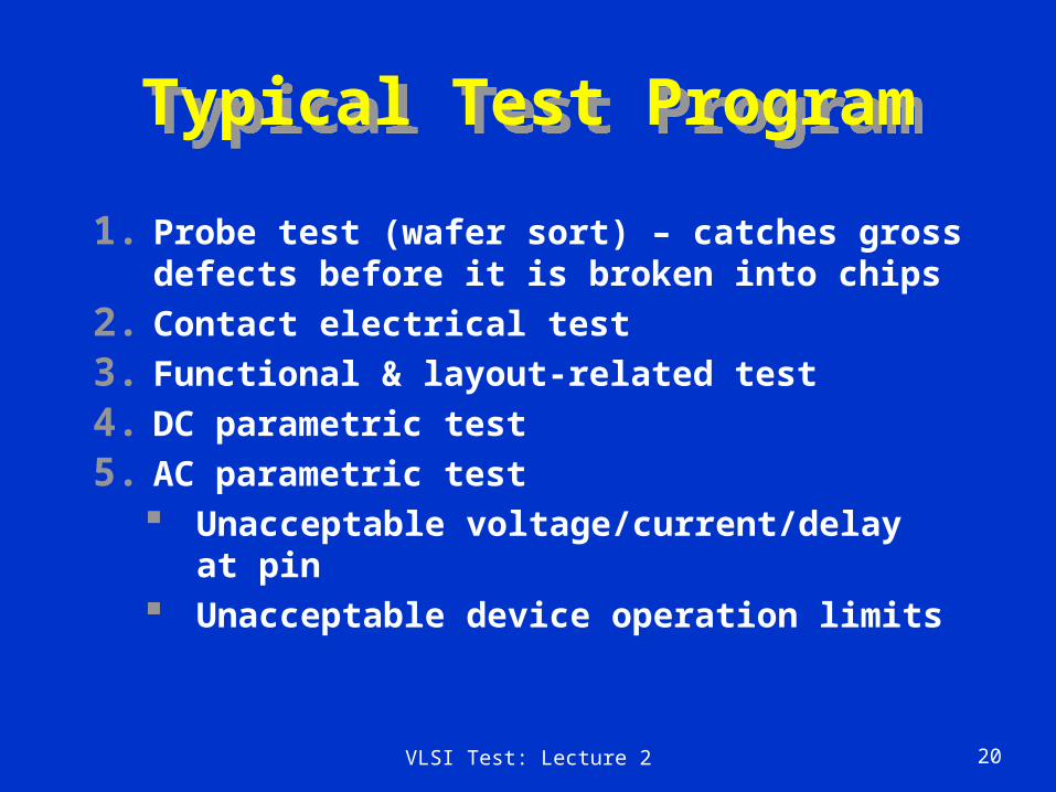
Typical Test ProgramTypical Test Program
1. Probe test (wafer sort) – catches gross defects before it is broken into chips
2. Contact electrical test
3. Functional & layout-related test
4. DC parametric test
5. AC parametric test Unacceptable voltage/current/delay at pin Unacceptable device operation limits
VLSI Test: Lecture 2 21
DC Parametric TestsDC Parametric Tests
VLSI Test: Lecture 2 22
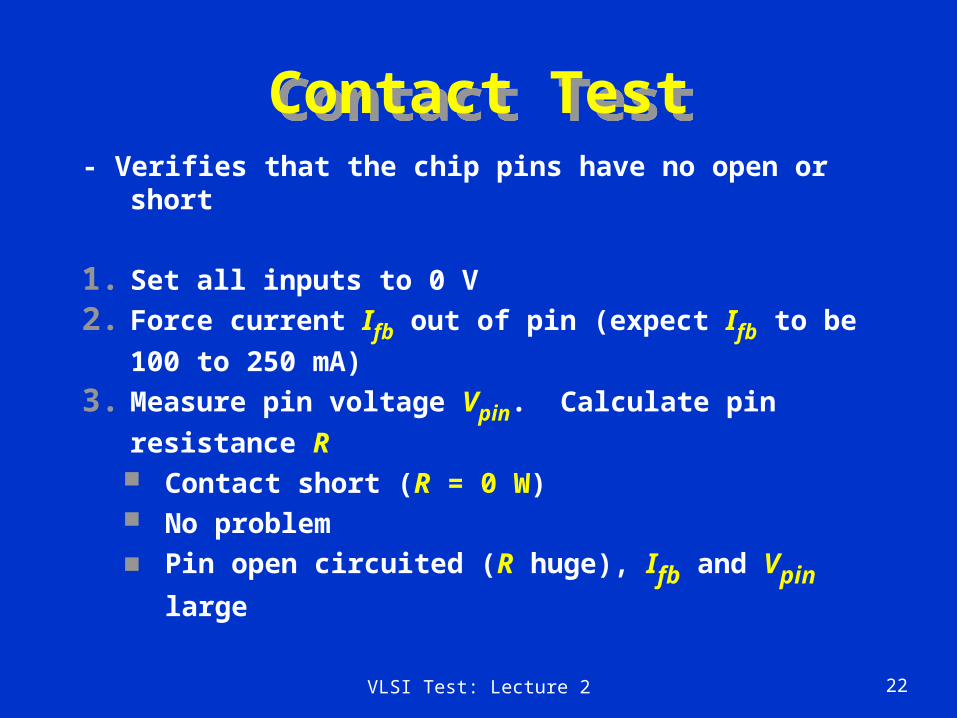
Contact TestContact Test- Verifies that the chip pins have no open or short
1. Set all inputs to 0 V
2. Force current Ifb out of pin (expect Ifb to be 100
to 250 mA)
3. Measure pin voltage Vpin. Calculate pin
resistance R Contact short (R = 0 W) No problem
Pin open circuited (R huge), Ifb and Vpin large
VLSI Test: Lecture 2 23
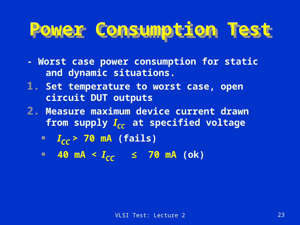
Power Consumption Test
Power Consumption Test
- Worst case power consumption for static and dynamic situations.
1. Set temperature to worst case, open circuit DUT outputs
2. Measure maximum device current drawn from supply ICC at specified voltage
ICC > 70 mA (fails)
40 mA < ICC ≤ 70 mA (ok)
VLSI Test: Lecture 2 24
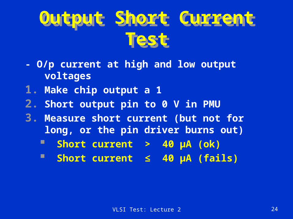
Output Short Current Test
Output Short Current Test
- O/p current at high and low output voltages
1. Make chip output a 1
2. Short output pin to 0 V in PMU
3. Measure short current (but not for long, or the pin driver burns out)
Short current > 40 μA (ok) Short current ≤ 40 μA (fails)
VLSI Test: Lecture 2 25
Output Drive Current Test
Output Drive Current Test
- For a output specified current o/p voltage must be maintained
1. Apply vector forcing pin to 0
2. Simultaneously force VOL voltage and measure IOL
3. Repeat Step 2 for logic 1
IOL < 2.1 mA (fails)
IOH < -1 mA (fails)
VLSI Test: Lecture 2 26
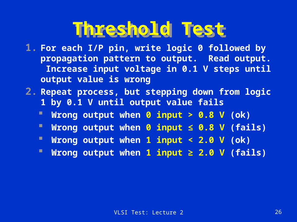
Threshold TestThreshold Test1. For each I/P pin, write logic 0 followed by
propagation pattern to output. Read output. Increase input voltage in 0.1 V steps until output value is wrong
2. Repeat process, but stepping down from logic 1 by 0.1 V until output value fails Wrong output when 0 input > 0.8 V (ok) Wrong output when 0 input ≤ 0.8 V (fails) Wrong output when 1 input < 2.0 V (ok) Wrong output when 1 input ≥ 2.0 V (fails)
VLSI Test: Lecture 2 27
AC Parametric TestsAC Parametric Tests
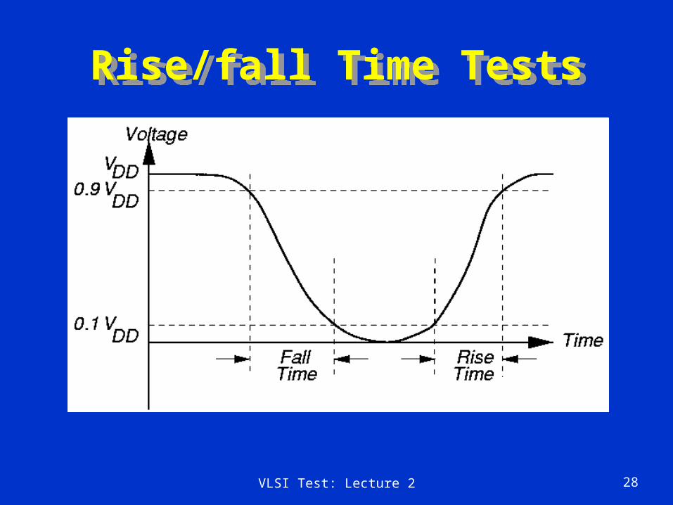
VLSI Test: Lecture 2 28
Rise/fall Time TestsRise/fall Time Tests
VLSI Test: Lecture 2 29
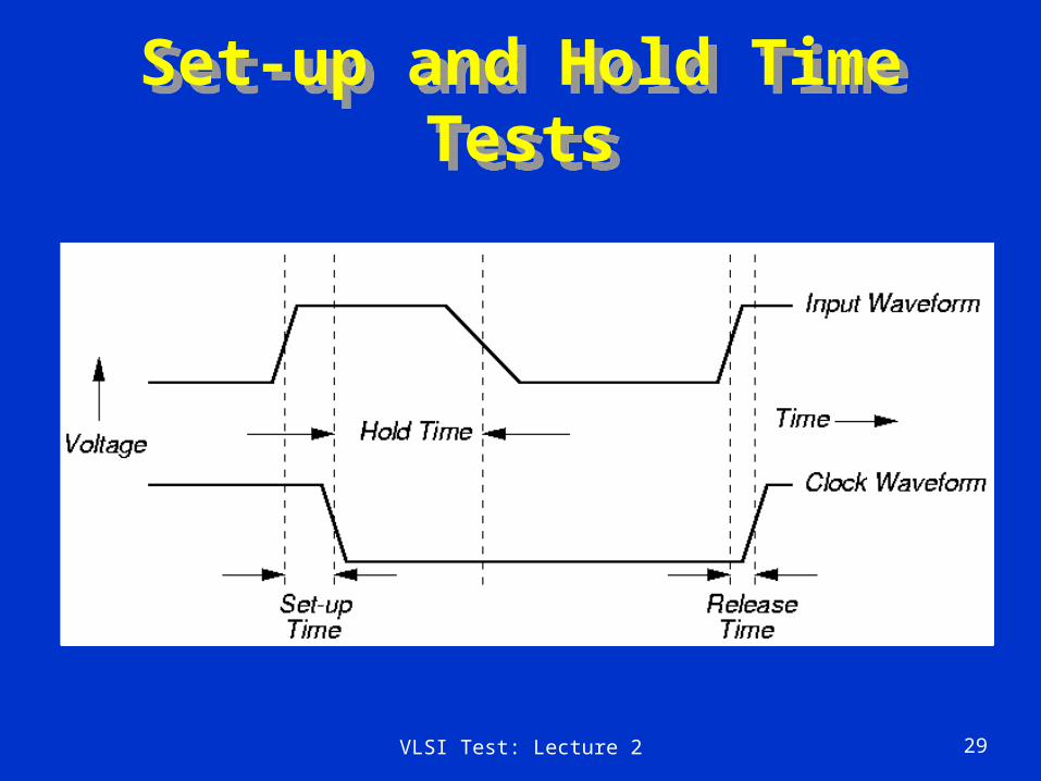
Set-up and Hold Time Tests
Set-up and Hold Time Tests
VLSI Test: Lecture 2 30
Propagation Delay Tests
Propagation Delay Tests
1. Apply standard output pin load (RC or RL)
2. Apply input pulse with specific rise/fall
3. Measure propagation delay from input to output Delay between 5 ns and 40 ns (ok) Delay outside range (fails)
ATE Cost Problems Pin inductance (expensive probing) Multi-GHz frequencies High pin count (1024)
ATE Cost Reduction Multi-Site Testing DFT methods like Built-In Self-Test
VLSI Test: Lecture 3 32
Lecture 3Test Economics
Lecture 3Test Economics
Economics defined
Costs
Production
Benefit - cost analysis
Economics of design-for-testability (DFT)
Quality and yield loss
Summary
VLSI Test: Lecture 3 33
The Meaning of Economics
The Meaning of Economics
Economics is the study of how men choose touse scarce or limited productive resources(land, labor, capital goods such as machinery,and technical knowledge) to produce variouscommodities (such as wheat, overcoats, roads,concerts, and yachts) and to distribute themto various members of society for theirconsumption.
-- Paul Samuelson
VLSI Test: Lecture 3 34
Engineering EconomicsEngineering Economics
Engineering Economics is the study of howengineers choose to optimize their designsand construction methods to produce objects and systems that will optimize their efficiency and hence the satisfaction of their clients.
VLSI Test: Lecture 3 35
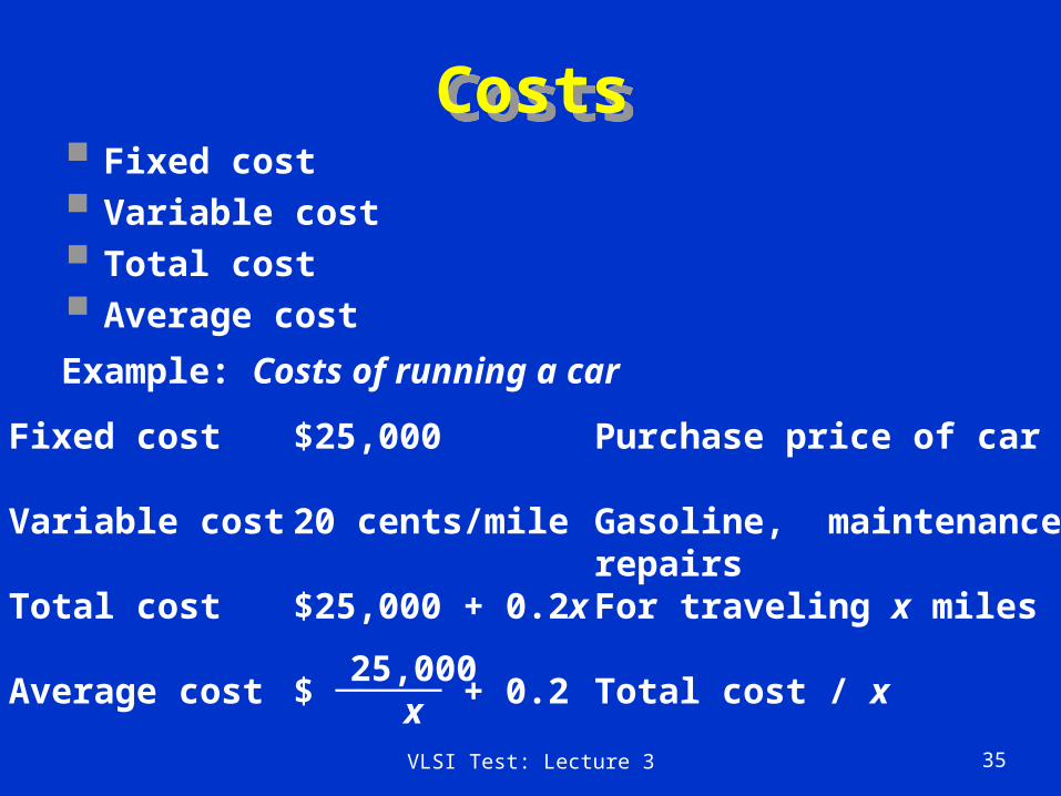
CostsCosts Fixed cost
Variable cost
Total cost
Average cost
Example: Costs of running a car
Fixed cost
Variable cost
Total cost
Average cost
$25,000
20 cents/mile
$25,000 + 0.2x
$ ───── + 0.225,000
x
Purchase price of car
Gasoline, maintenance,repairsFor traveling x miles
Total cost / x
VLSI Test: Lecture 3 36
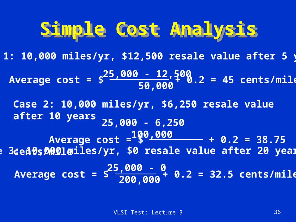
Simple Cost AnalysisSimple Cost AnalysisCase 1: 10,000 miles/yr, $12,500 resale value after 5 years
Case 2: 10,000 miles/yr, $6,250 resale value after 10 years
Average cost = $ ───────── + 0.2 = 38.75 cents/mile
Case 3: 10,000 miles/yr, $0 resale value after 20 years
Average cost = $ ─────── + 0.2 = 32.5 cents/mile
25,000 - 6,250 100,000
25,000 - 0 200,000
VLSI Test: Lecture 3 37
Example: A PCB Repair ShopExample: A PCB Repair Shop
Average cost of repair = $350, includes Cost of diagnostic test = $300 Cost of replacement chip = $ 10 Cost of assembly and test = $ 40
Failure data for 100 chips on PCB Chip A failure rate = 90% Chip B failure rate = 90% Collective failure rate for chips A and B
= 0.9 + 0.9 – 0.81 = 0.99
VLSI Test: Lecture 3 38
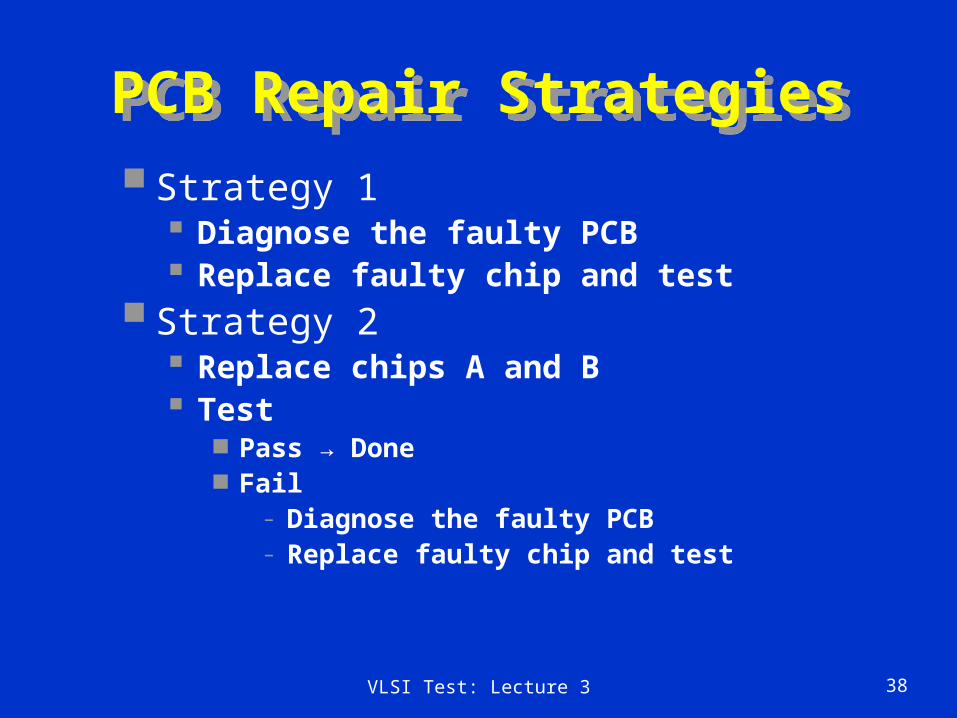
PCB Repair StrategiesPCB Repair Strategies
Strategy 1 Diagnose the faulty PCB Replace faulty chip and test
Strategy 2 Replace chips A and B Test
Pass → Done Fail
– Diagnose the faulty PCB– Replace faulty chip and test
VLSI Test: Lecture 3 39
PCB Repair StrategiesPCB Repair Strategies
Faulty PCB
Apply diagnosticTest
Cost = $300
Replace faultyChip and testCost = $50
Faulty PCB
Replace chipsA and B and test
Cost = $60
Replace faultyChip and testCost = $50
PCB passesTest?
Apply diagnosticTest
Cost = $300
Repair completedAv. Cost = $63.50
Repair completedAv. Cost = $350.50
Yes Prob=0.99
No
Prob=0.01
Strategy 1
Strategy 2
VLSI Test: Lecture 3 40
Economics of Design for Testability (DFT)Economics of Design for Testability (DFT)
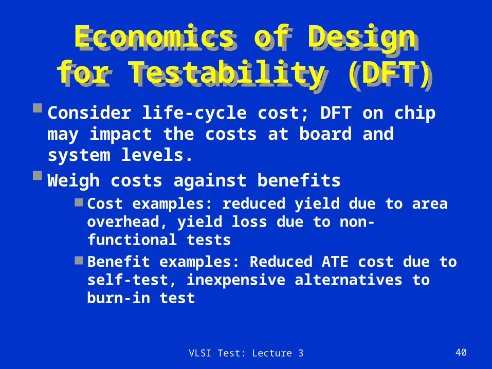
Consider life-cycle cost; DFT on chip may impact the costs at board and system levels.
Weigh costs against benefits Cost examples: reduced yield due to area
overhead, yield loss due to non-functional tests Benefit examples: Reduced ATE cost due to
self-test, inexpensive alternatives to burn-in test
VLSI Test: Lecture 3 41
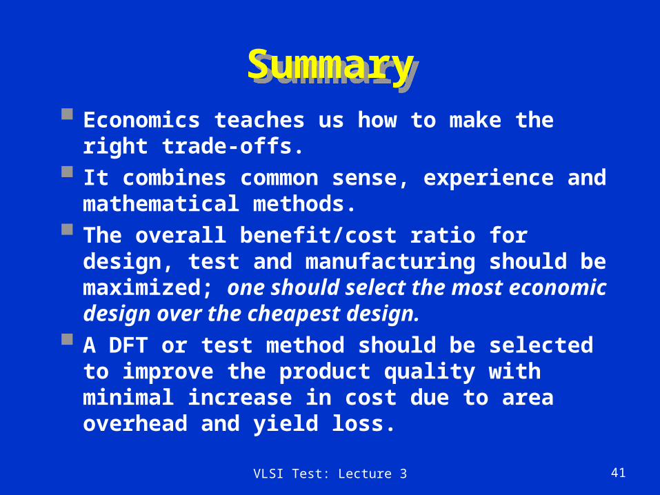
SummarySummary Economics teaches us how to make the right
trade-offs.
It combines common sense, experience and mathematical methods.
The overall benefit/cost ratio for design, test and manufacturing should be maximized; one should select the most economic design over the cheapest design.
A DFT or test method should be selected to improve the product quality with minimal increase in cost due to area overhead and yield loss.
VLSI Test: Lecture 4 42
Lecture 4Yield Analysis and Product
Quality
Lecture 4Yield Analysis and Product
Quality
Yield and manufacturing cost
Clustered defect yield formula
Defect level
Test data analysis
Example: SEMATECH chip
Summary
VLSI Test: Lecture 4 43
VLSI Chip YieldVLSI Chip Yield
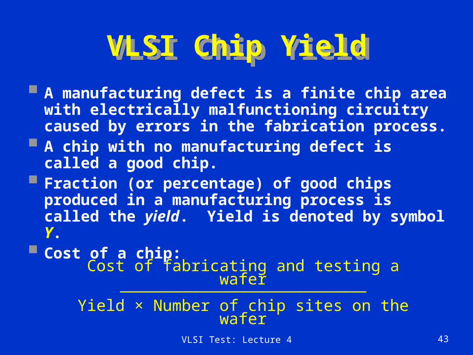
A manufacturing defect is a finite chip area with electrically malfunctioning circuitry caused by errors in the fabrication process.
A chip with no manufacturing defect is called a good chip.
Fraction (or percentage) of good chips produced in a manufacturing process is called the yield. Yield is denoted by symbol Y.
Cost of a chip:
Cost of fabricating and testing a wafer──────────────────────────
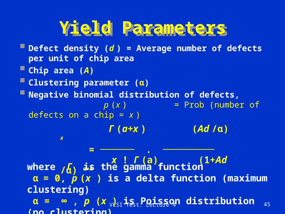
Yield ParametersYield Parameters Defect density (d ) = Average number of defects per
unit of chip area
Chip area (A)
Clustering parameter (α)
Negative binomial distribution of defects, p (x ) = Prob (number of defects on a chip = x )
Γ (a+x ) (Ad /α) x
= ────── . ───────── x ! Γ (a) (1+Ad /α) α+x
where Γ is the gamma function α= 0, p (x ) is a delta function (maximum clustering) α = ∞ , p (x ) is Poisson distribution (no clustering)
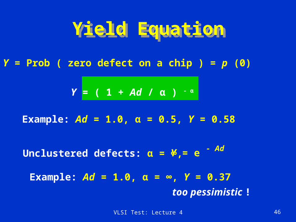
VLSI Test: Lecture 4 46
Yield EquationYield Equation
Y = Prob ( zero defect on a chip ) = p (0)
Y = ( 1 + Ad / α ) - α
Example: Ad = 1.0, α = 0.5, Y = 0.58
Unclustered defects: α = ∞, Y = e - Ad
Example: Ad = 1.0, α = ∞, Y = 0.37
too pessimistic !
VLSI Test: Lecture 4 47
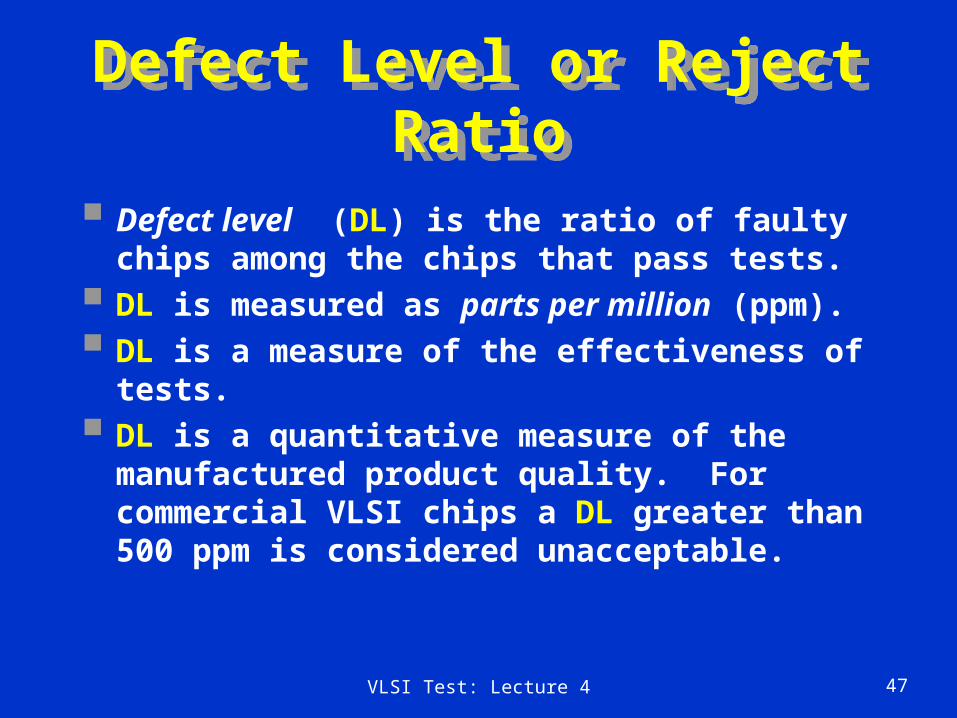
Defect Level or Reject RatioDefect Level or Reject Ratio
Defect level (DL) is the ratio of faulty chips among the chips that pass tests.
DL is measured as parts per million (ppm).
DL is a measure of the effectiveness of tests.
DL is a quantitative measure of the manufactured product quality. For commercial VLSI chips a DL greater than 500 ppm is considered unacceptable.
VLSI Test: Lecture 4 48
Determination of DLDetermination of DL
From field return data: Chips failing in the field are returned to the manufacturer. The number of returned chips normalized to one million chips shipped is the DL.
From test data: Fault coverage of tests and chip fallout rate are analyzed. A modified yield model is fitted to the fallout data to estimate the DL.
VLSI Test: Lecture 4 49
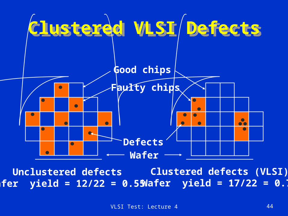
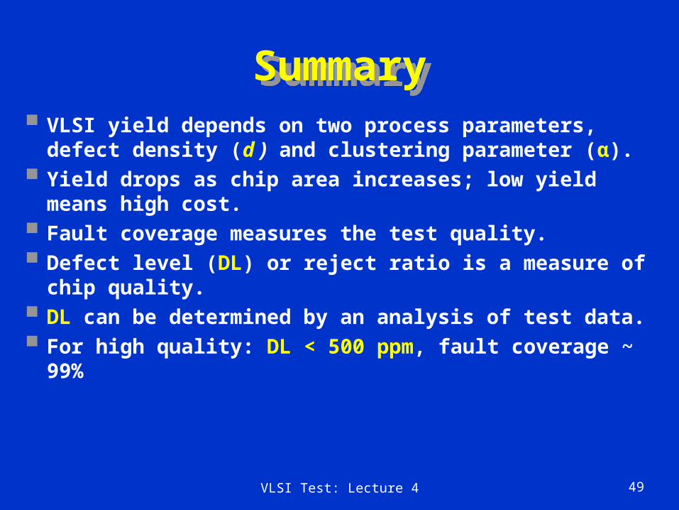
SummarySummary VLSI yield depends on two process parameters, defect
density (d ) and clustering parameter (α).
Yield drops as chip area increases; low yield means high cost.
Fault coverage measures the test quality.
Defect level (DL) or reject ratio is a measure of chip quality.
DL can be determined by an analysis of test data.
For high quality: DL < 500 ppm, fault coverage ~ 99%