Testing To Investigate Stress-Lifetime Characteristics Of High Voltage Printed Circuit Boards IEPC-2015-b-490p Presented at Joint Conference of 30th International Symposium on Space Technology and Science 34th International Electric Propulsion Conference and 6th Nano-satellite Symposium, Hyogo-Kobe, Japan July 4 – 10, 2015 Oliver El Korashy 1 and Andreas Franke 2 ESA, TEC-EP Keplerlaan 1, Noordwijk Zh, 2201AZ, Netherlands Matthias Gollor 3 ESA, EOP-PX Keplerlaan 1, Noordwijk Zh, 2201AZ, Netherlands Abstract: Printed circuit boards (PCBs) are typically used in all electronic equipment, including those conditioning or controlling high voltage (HV) for space satellite applications. With the use of new subsystems that require higher voltages (generally several hundred volts up to tens of kV), stress-lifetime issues are becoming more complex. In order to allow compact design and cost efficient production of HV modules, there is an increasing demand to improve the design of PCBs with encapsulation or conformal coating at higher voltages. Within a PCB there are a number of electrical field interfaces each of which can have individual stress-lifetime characteristics, and the influence of environmental aging should also be considered, which means a large number of sample types should be tested to gain experimental evidence to define the margin for each interface. This paper demonstrates a method to test multiple samples at a fixed DC voltage stress until the event of a breakdown, and presents test results from 6 single-sided encapsulated PCB samples. I. Introduction N the space industry high voltage (HV) modules are produced with different packaging techniques and different uses of printed circuit boards (PCBs) for the various applications which include: communication travelling wave tube amplifiers, electric propulsion power conditioning electronics, instrument radar tube amplifiers, and scientific experiments 1 . Due to an increasing demand of HV applications for space, there is a growing desire to gain more knowledge of design rule margins and extend the range of use for PCBs at higher voltages. The number of criterion that apply to HV PCB design for space applications are extensive and include: single sided, double sided, multilayer, slots in the substrate, surface treatments, guard rings, component footprint shapes, flooding holes, visibility optimization and solder joint shapes. Samples are defined according to PCB substrate material, track thickness and encapsulation (potting) or conformal coating material. The aging factors that can influence the HV stress-lifetime of the samples include humidity and temperature (constant or cycling). As the temperature can affect the breakdown voltage, HV stress-lifetime testing should be done in the qualification temperature range. For a comprehensive knowledge of HV stress-lifetime which considers all criterion with all materials and environmental aging conditions, a huge number of samples are required. To derive a stress life-time curve, endurance testing at a minimum of 3 voltages is needed. It is expected that breakdown testing at the lowest voltage level takes at least 3 months. Testing a large amount of samples simultaneously means tests can be completed and results presented in an acceptable timeframe. 1 Power Conditioning Engineer, Power Management and Distribution, [email protected]2 High-Voltage and Power Conditioning Engineer, Power Management and Distribution, [email protected]3 Principal Electrical Engineer, Earth Observation Projects, [email protected]I Joint Conference of 30th ISTS, 34th IEPC and 6th NSAT, Kobe-Hyogo, Japan July 4 – 10, 2015 1
Transcript
Testing To Investigate Stress-Lifetime Characteristics Of High Voltage Printed Circuit Boards
IEPC-2015-b-490p
Presented at Joint Conference of 30th International Symposium on Space Technology and Science34th International Electric Propulsion Conference and 6th Nano-satellite Symposium,
Hyogo-Kobe, JapanJuly 4 – 10, 2015
Oliver El Korashy1 and Andreas Franke2
ESA, TEC-EP Keplerlaan 1, Noordwijk Zh, 2201AZ, Netherlands
Matthias Gollor3
ESA, EOP-PX Keplerlaan 1, Noordwijk Zh, 2201AZ, Netherlands
Abstract: Printed circuit boards (PCBs) are typically used in all electronic equipment, including those conditioning or controlling high voltage (HV) for space satellite applications. With the use of new subsystems that require higher voltages (generally several hundred volts up to tens of kV), stress-lifetime issues are becoming more complex. In order to allow compact design and cost efficient production of HV modules, there is an increasing demand to improve the design of PCBs with encapsulation or conformal coating at higher voltages. Within a PCB there are a number of electrical field interfaces each of which can have individual stress-lifetime characteristics, and the influence of environmental aging should also be considered, which means a large number of sample types should be tested to gain experimental evidence to define the margin for each interface. This paper demonstrates a method to test multiple samples at a fixed DC voltage stress until the event of a breakdown, and presents test results from 6 single-sided encapsulated PCB samples.
I. IntroductionN the space industry high voltage (HV) modules are produced with different packaging techniques and different uses of printed circuit boards (PCBs) for the various applications which include: communication travelling wave
tube amplifiers, electric propulsion power conditioning electronics, instrument radar tube amplifiers, and scientific experiments1. Due to an increasing demand of HV applications for space, there is a growing desire to gain more knowledge of design rule margins and extend the range of use for PCBs at higher voltages.
The number of criterion that apply to HV PCB design for space applications are extensive and include: single sided, double sided, multilayer, slots in the substrate, surface treatments, guard rings, component footprint shapes, flooding holes, visibility optimization and solder joint shapes. Samples are defined according to PCB substrate material, track thickness and encapsulation (potting) or conformal coating material. The aging factors that can influence the HV stress-lifetime of the samples include humidity and temperature (constant or cycling). As the temperature can affect the breakdown voltage, HV stress-lifetime testing should be done in the qualification temperature range. For a comprehensive knowledge of HV stress-lifetime which considers all criterion with all materials and environmental aging conditions, a huge number of samples are required. To derive a stress life-time curve, endurance testing at a minimum of 3 voltages is needed. It is expected that breakdown testing at the lowest voltage level takes at least 3 months. Testing a large amount of samples simultaneously means tests can be completed and results presented in an acceptable timeframe.
1 Power Conditioning Engineer, Power Management and Distribution, [email protected] High-Voltage and Power Conditioning Engineer, Power Management and Distribution, [email protected] Principal Electrical Engineer, Earth Observation Projects, [email protected]
I
Joint Conference of 30th ISTS, 34th IEPC and 6th NSAT, Kobe-Hyogo, JapanJuly 4 – 10, 2015
1
ESA has a strong motivation to provide industry with a clear design philosophy and justified safety margins on existing and new technologies, compiled into a new published standard or guideline which would aim to improve the work flow and design of HV PCBs. The work described herein demonstrates the development of a test setup which is able to long-term breakdown (BD) test up to 90 samples simultaneously and is the first stage of a study to assess different HV PCB solutions on the basis of statistical evaluation of life test data.
The principle method used by the test setup described herein, is to apply a fixed DC high voltage to samples until a breakdown inside the isolation material occurs. Depending on the application, the rules for a PCB design may need to be defined for each voltage type including direct current (DC), pulsed, and alternating current (AC). Testing at DC voltage was selected based on the following rationale: a) space HV PCBs usually have to deal with DC voltages as one of the main applications, b) this is a baseline study, c) test setup simplicity.
For statistical evaluation of an intrinsic property of a PCB design it is important to have a test sample which is not sensitive to any unwanted side effects. For example, in order to measure the strengths of the insulations gap between two parallel PCB tracks the sample should breakdown in the area of the parallel tracks and not at the connections to the terminal or at curvature tracks of internal interconnection. Furthermore, in order to determine a stress-lifetime curve the sample should be able to be tested at HV level to detect the short-term breakdown. For example, a 1mm gap in PCB encapsulated in epoxy is likely to have a short-term capability of 50 kV or higher, but might fail in long-term at much lower voltages after many years. Consequently the sample needs to have a simple geometry in the area under investigation, and needs to be easily reproducible with different substrate and encapsulation materials. It should be small enough to allow parallel testing of many samples but must be large enough to avoid breakdown in the surrounding air environment.
Therefore, a PCB was designed that is able to test the characteristics across the tracks of a single sided PCB, using a 1mm spacing between the terminals. 6 of these samples were encapsulated in an epoxy resin, and 1 of these samples was tested with a short-term break down test. Afterwards, it has been analyzed to locate the origin of the breakdown and to trace its path was performed on the sample, which broke down at 27.62kV. The other 5 samples were simultaneously long-term breakdown tested at 20kV and the time until breakdown was recorded. 20kV was selected on the rationale that it is 72% of the breakdown voltage so all samples would endure the voltage stress for some time before breakdown.
In terms of similar published research, some investigations have been made into HV stress aging on epoxy insulation and the papers are listed in the references. None of this research is considering space applications or PCBs designed for use in space. Therefore the investigation into HV PCB stresses and aging has been performed before by individual space companies, but is so far
Figure 1. Breakdown location in a potted single sided PCB under HV stress.
Figure 2. Field strength for a 1mm gap between tracks including a rounded shape for termination.
Figure 3. The bare PCB sample – single sided 70μm tinned copper on FR4 substrate with 1mm spacing.
Joint Conference of 30th ISTS, 34th IEPC and 6th NSAT, Kobe-Hyogo, JapanJuly 4 – 10, 2015
2
unexplored by formal peer reviewed research. There is an existing ECSS standard which applies to design and procuring of PCBs, ECSS-Q-ST-70-11C (soon to be superseded by ECSS-Q-ST-70-12C which covers PCBs working up to 500V). There is also information regarding HV PCB design contained in Ref. 1.
II. Description and Rationale of Study Method
A. HV PCB Test Sample DesignBetween the parallel tracks of a PCB, it is
assumed that the weakest point of the insulation isthe direct path lateral to the surface of the PCB and between the two tracks of different voltage, as shown in Fig. 1. This has to be proven for different encapsulation and substrate materials.
In order to achieve a significant length of this insulating gap a layout with a meander shaped track was chosen. By using finite element (FEM) analysis the shape of the terminating ends and bends of the tracks are optimized to avoid significant field enhancement at that location. As mentioned above it is useful to have a test sample which is stressed to a maximum in the areas under investigation, which are the parallel tracks and not the curvatures, terminations and terminals. Fig. 2 shows the result of this optimization – there is only a small enhancement of the electrical field at the curvatures.
B. Tested Sample DescriptionThe PCB design of the test sample is shown in
Fig. 3. As intended it provides a number of parallel tracks of 1mm distance, which is connected to terminals allowing the application of a voltage difference. The figure shows a single layer PCB, however a similar configuration might be also be realized as double sided or multilayer, depending on the objectives of further investigations.
The bare PCB samples, were designed and procured according to standard ECSS-Q-ST-70-11C and were manufactured by an ESA qualified contractor. The dimensions are 220mm x 100mm x 1.6mm. The materials selected were FR4 (flame retardant glass-reinforced epoxy) PCB substrate with 70μm tinned copper printing.
As the concept of the intended study is focused on the composite of a PCB substrate with tracks, and an encapsulation material, a fully potted version was made and is shown in Fig. 4. These samples were potted in a filled epoxy resin by an ESA qualified contractor. Screening of the completed samples was limited to confirming the resistance between the terminals was greater than
-ray radiography.
C. ESA Long Life Test FacilityBased on the above sample design and
definition, an ESA long life lest facility was defined, developed and validated. The objective is for the facility to be capable to test a high number of samples in parallel to allow a statistical
Figure 4. The potted PCB sample – bare PCB sample encapsulated in epoxy resin.
DC HVPOWER SUPPLY PCB SAMPLE
BDU
+
+-
-
ISOLATEDDIGITAL SIGNAL
DATAACQUISITION
UNIT
OPU
Figure 5. Principle of endurance HV stress test and breakdown detection.
Uin
Uout
0V 0V
VaristorS20K30
TVS8.2V
R100Ohm
Figure 6. Schematic of OPU.
Joint Conference of 30th ISTS, 34th IEPC and 6th NSAT, Kobe-Hyogo, JapanJuly 4 – 10, 2015
3
evaluation under thermal cycling and high voltage stress.
General experience from high voltage breakdown test indicates that there might be a high scatter in the test results. This leads to the assumption that a minimum of 5 to 10 samples of identical type need to be tested under the same conditions. Furthermore, in order to allow assessment of types of samples, it was finally decided to allow simultaneous testing of up to 90 samples. This had been defined as a compromise in view of the available space in an available thermal cycling chamber. It was required to have an autonomously running long life test setup. Therefore it was specified to have an individual breakdown detection per sample.
Fig. 5 shows a basic block diagram of the test setup. The diagram shows how a breakdown in a sample is detected and the digital signal acquired. The positive terminals of the samples are connected to the HV power supplyoutput and each negative terminal is shunted to ground via a circuit called the “overvoltage protection unit” (OPU). The schematic of the OPU is shown in Fig. 6. In the event of a breakdown, the breakdown current passes through a varistor which has a clamping voltage of 90V. Across the varistor, a resistor is connected in series with a transient voltage suppressor (TVS) 8.2V zener diode. In the event of a breakdown of the sample, the varistor conducts the majority of the breakdown current, and the lower power TVS absorbs the remaining current, generating a 8.2V signal pulse across the zener diode.
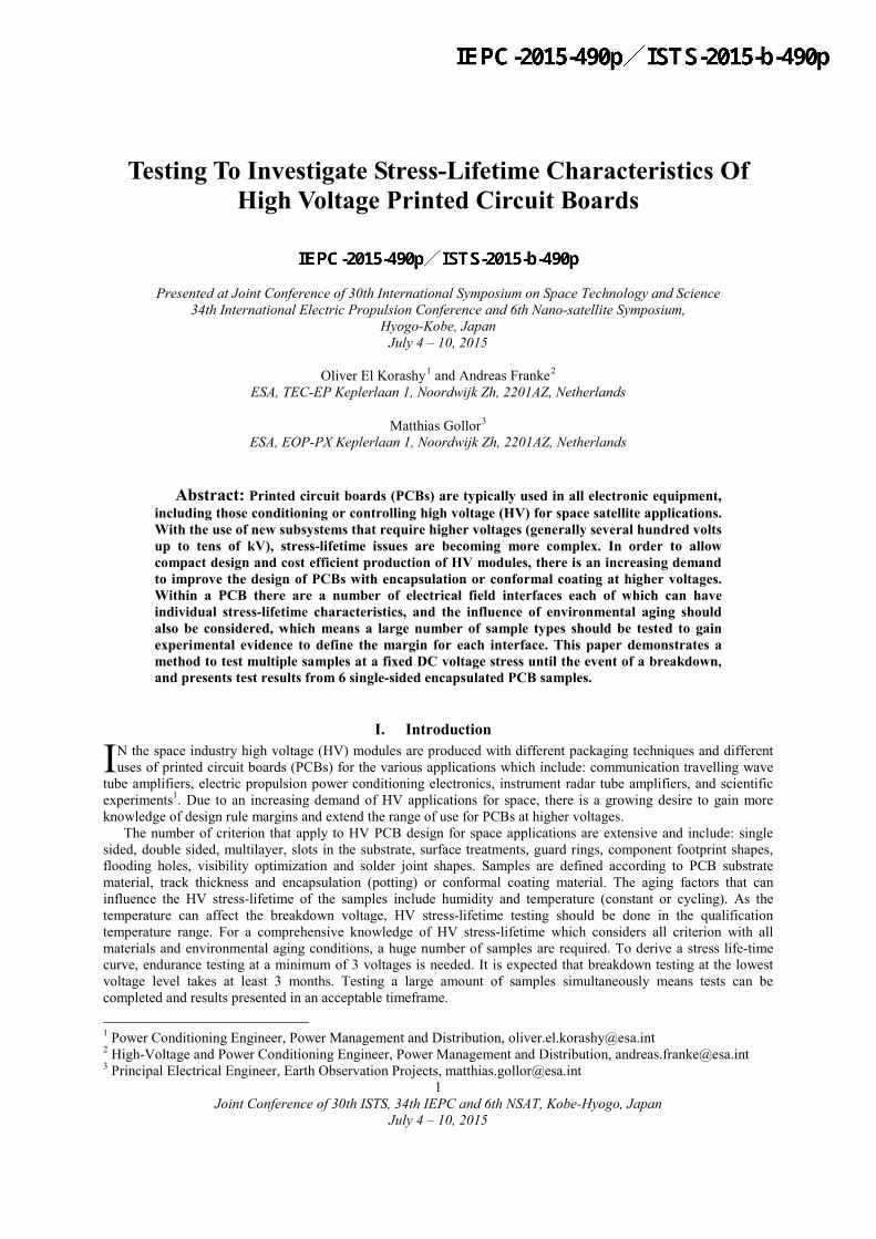
The output of the OPU is connected to a circuit called the “breakdown detection unit” (BDU) which is designed to interface with the signal pulse generated by the OPU to produce a latching digital isolated output with a LED visual display. The BDU has been designed into a rack mounted unit with 90 channels. A schematic of a single channel is shown in Fig. 7. To prevent damage to digital circuitry, isolation between the HV ground and digital ground is required. For this reason the circuit features two grounds and DC auxiliary power supplies, and an optocoupler is used to provide galvanic isolation between the input and output. The pulse generated by the OPU stimulates the input of the BDU channel which results in the triggering of the latching of a flip-flop.
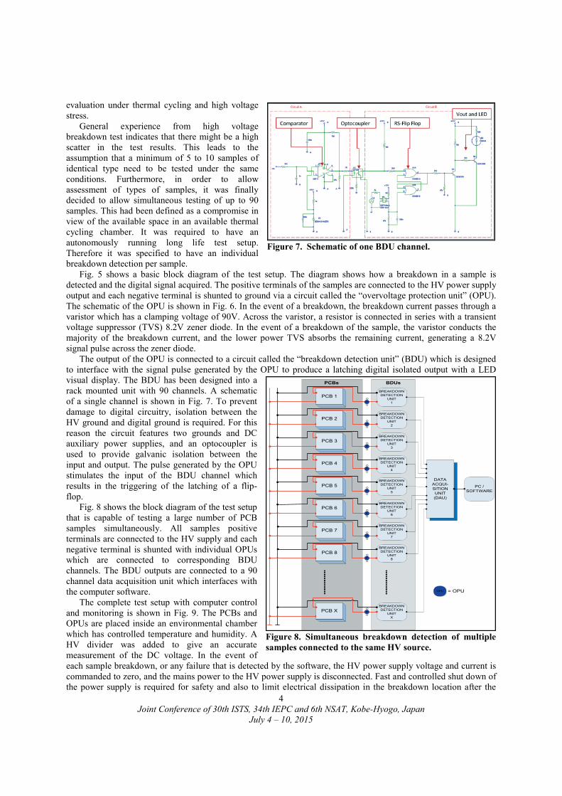
Fig. 8 shows the block diagram of the test setup that is capable of testing a large number of PCB samples simultaneously. All samples positive terminals are connected to the HV supply and each negative terminal is shunted with individual OPUs which are connected to corresponding BDU channels. The BDU outputs are connected to a 90 channel data acquisition unit which interfaces with the computer software.
The complete test setup with computer control and monitoring is shown in Fig. 9. The PCBs and OPUs are placed inside an environmental chamberwhich has controlled temperature and humidity. A HV divider was added to give an accurate measurement of the DC voltage. In the event of each sample breakdown, or any failure that is detected by the software, the HV power supply voltage and current is commanded to zero, and the mains power to the HV power supply is disconnected. Fast and controlled shut down of the power supply is required for safety and also to limit electrical dissipation in the breakdown location after the
Figure 7. Schematic of one BDU channel.………….
PCB 1
PCB 3
PCB 5
PCB 4
PCB 2
PCB 6
PCB 7
PCB 8
PCB X
PCBs
BREAKDOWNDETECTION
UNIT1
BREAKDOWNDETECTION
UNIT2
BREAKDOWNDETECTION
UNIT3
BREAKDOWNDETECTION
UNIT4
BREAKDOWNDETECTION
UNIT5
BREAKDOWNDETECTION
UNIT6
BREAKDOWNDETECTION
UNIT7
BREAKDOWNDETECTION
UNIT8
BREAKDOWNDETECTION
UNITX
DATAACQUI-SITIONUNIT(DAU)
PC /SOFTWARE
BDUs
………….
OPU
OPU
OPU
OPU
OPU
OPU
OPU
OPU
OPU
OPU = OPU
Figure 8. Simultaneous breakdown detection of multiple samples connected to the same HV source.
Joint Conference of 30th ISTS, 34th IEPC and 6th NSAT, Kobe-Hyogo, JapanJuly 4 – 10, 2015
4
breakdown has occurred. All components that share the HV ground are star connected and a single connection made between the star point and the main building earth.
The computer software controls:- HV power supply mains On/Off- HV power supply current limit- HV power supply voltage
The computer software monitors:- HV power supply current read back- HV power supply voltage read back- voltage divider- BDU channels- time- temperature- humidity
Error alarms are set to immediately shut down the HV power system in the following events:
- HV power supply current read back out of limit (OOL)
- HV power supply voltage read back OOL- voltage divider OOL- error current threshold exceeded- BDU event detected- software crash- computer crash
The software sends the command to set the DC voltage and current limit level of the HV power supply, commanding the gradual increase in step increments. The software error current threshold setting is implemented as a 2nd mechanism to detect sample failure – by setting the threshold level to detect if any sample fails to low impedance. HV measurements and criticalmonitoring are using the voltage divider output which is more accurate, faster and reliable than the power supply voltage read back.
For the breakdown tests in chapters 5 and 6 of this paper, the current limit was set to 0.5mA and the current alarm limit was set to 0.3mA, and the environmental conditions were controlled at temperature of 20°C (+/- 5%) and 45% (+/- 10%) relative humidity (RH). Prior to HV stress testing, the samples were stored at ambient conditions in the Netherlands for approximately 12 months.
In the event of a breakdown the surge current occurs too fast for the output current limitation mechanism of the power supply to have any action. Therefore the energy that is discharged by the breakdown is determined by the output impedance of the power supply, combined with the impedances the cable, HV rails, samples connected, and voltage divider.
D. Short-Term Breakdown Test and Sample Analysis
For reference, a bare PCB in Fig. 3 was tested using the setup in Fig. 9, increasing the voltage by 100V every 30 seconds until a breakdown is detected by the test setup. The breakdown was detected by the BDU at 1.77kV. The resistance was measured and was still the same as before the
Figure 9. Full system block diagram (showing only 1 PCBsample under test).
Figure 10. Identify breakdown location by thermal imaging of resistive power dissipation.
Figure 11. X-ray radiography of breakdown observed from underside and top side of PCB.
Joint Conference of 30th ISTS, 34th IEPC and 6th NSAT, Kobe-Hyogo, JapanJuly 4 – 10, 2015
5
with exactly the same results.Next a potted PCB sample in Fig. 4 was
subjected to the same tests as above, and the breakdown event was measured when voltage applied was 27.62kV. After breakdown the resistance across the terminalThe sample was then imaged with X-ray radiography to try to determine the location of the breakdown, but it was unsuccessful because the sample size was too large in relation to the small size of the breakdown. An investigative method was applied to find the approximate location: byapplying a low DC voltage across the sample terminals while thermal imaging to see if the heat dissipation in the
iled insulation could be observed.The applied voltage was 3V for 1 minute, which results in current of 3mA, power dissipation of 3mW and a total
absorbed energy of 180mJ. The image taken at 1 minute is shown in Fig. 10, and a dissipative hot spot is clearly visible. After this test had been performed the resistance measured acrosless than the measurement taken directly after breakdown which suggests that the test may have affected the sample.
With the approximate possible breakdown location identified, X-ray radiography was performed again at a higher resolution and focused on the suspect area. This time the possible breakdown location was found and images were taken from the underside and topside of the PCB sample, shown in Fig. 11. A circular feature was observed in the 1mm spacing between the tracks, which indicated slight damage to the edge of the PCB tracks with a change of state in the insulation materials between them.
With the precise location now visible, it was possible to take a more detailed look by destructive parts analysis, by taking two micro section slices at normal angle to the PCB substrate top surface. Two positions for micro section were selected, as seen in Fig. 12, one is just outside where the breakdown occurred (Pos 1) and one is through the center of the breakdown (Pos 2).
The cross section just outside of the circular feature, shown in Fig. 13, revealed evidence of separation of the PCB substrate glass fiber layers just below the surface, which can possibly be resulting from dissipation of the breakdown current leading to thermal-mechanical stresses deforming the insulation materials.
The cross section taken then directly though the center, shown in Fig. 14, revealed a build-up of carbonized insulation material around the breakdown location. The extensive heat damage suggests there was electrical overstress as a consequence of the dielectric breakdownconducting after the initial arc. It is suggested that the breakdown path was approximately through the center of the circular feature, based on the assumption that heat damage propagated from this location.
E. Long-Term Breakdown Test At 20kv5 encapsulated PCB samples were endurance tested in parallel with the test setup described by Fig. 9. The
voltage is increased from 0V in 250V steps, taking 11 minutes to reach 20kV. In the event of a breakdown, the system shuts down the HV power supply, and the broken down sample is removed and the resistance across the terminals is measured. Afterwards the HV power supply voltage is increased again to 20kV. The time until breakdown is recorded from when the 20kV is reached, up until the breakdown event. The time under voltage stress
Figure 12. Micro section locations, Position 1 and 2.
Figure 14. Micro section Pos 2, location of breakdown and build-up of carbonized material.
Joint Conference of 30th ISTS, 34th IEPC and 6th NSAT, Kobe-Hyogo, JapanJuly 4 – 10, 2015
6
is accumulated and for samples a – e is shown in Fig. 15. Note that sample b is still under test and as of the date 16 March 2014 it has lasted for 620 hours. For the 4 samples the resistance measured across the terminals was between
1 sample broke down after only 40 minutes, the next two lasted under 8 hours, but the other 2 samples lasted considerably longer: 1 broke down after 180 hours, and 1 is still surviving after 620 hours. High scattering could possibly be due to differences in sample quality. Furthermore, it is possible that testing at a lower voltage or testing after aging of samples would result in less scattering. Parts analysis data is not yet available for these samples.
F. Evaluation Of Test Setup And Suggestions For ImprovementsThere is a limitation of the setup in that it does not measure the energy of each breakdown. This could be
achieved by adding a current probe in the discharge path of the samples to ground. This probe would be connected to a digital storage oscilloscope, which triggered on a current level that is above the quiescent current, so that for each discharge a waveform capture occurs and hence the transient breakdown current that flows through the sample is measured. If the discharge energy was too high it could be limited by adding a series resistor to the HV power supply output. This test is useful for verification of the test setup onselected samples.
Visual inspection of the samples after the terminals had been soldered revealed a slight discoloration of the substrate near to the solder pad, and X-ray radiography of the samples after they had been potted revealed unwanted solder deposits on the tracks near to the pad where the terminals were soldered. The connecting terminals used were too heavy and required too much heat to solder which resulted in a risk of damaging the PCB substrate and track when soldering. Future PCB sample designs will use connecting terminals which require less heat to solder.
The screening for quality and consistency of the potted HV PCB samples could be improved by including isolation and partial discharge testing of each sample, prior to breakdown testing.
The samples were larger than necessary which means they are more expensive to produce and it is harder to find the breakdown location. It is recommended to reduce the sample size to reduce the cost of a large scale study.
For the identification of the breakdown location with thermal imaging, the energy dissipated should be reduced to the minimum possible. A low voltage should be used and the time duration controlled in order to limit the heat that the breakdown path absorbs, so that the temperature gradient on the sample is close to the temperature resolution of the thermal camera. For the follow up study, it has been decided though to use computed tomography imaging on selected samples, instead of the thermal method.
It is noted that each time a breakdown occurs, all of the samples connected in parallel are subjected to a transient of the HV decreasing to zero. This is unavoidable if testing samples in parallel connected to a single HV power supply and it is not expected that these transients can affect the HV stress to lifetime characteristic of the samples.
III. ConclusionThe test setup development is considered successful in that it has run autonomously for over 1 month and has
detected the breakdowns on 6 samples, with no anomaly or error events occurring. The principle of the design of a HV PCB sample to test a single electrical interface within a PCB has been
demonstrated successfully, with micro section analysis showing that the breakdown occurred in the 1mm spacing between the tracks.
Considering the broader objective, much research is to be done before a standardized set of PCB layout design rules are available for HV PCBs that are potted or conformably coated. ESA now has a test setup available to gain data for a comprehensive study that represents the different manufacturers in the European space industry and the different materials and processes that are used. This setup will be utilized in a long term study which will test over 500 samples of different types, including single sided PCB, double sided PCB, encapsulated insulation and
Figure 15. Time for breakdown for epoxy resin encapsulated FR4 single sided PCB with 1mm spacing.
Joint Conference of 30th ISTS, 34th IEPC and 6th NSAT, Kobe-Hyogo, JapanJuly 4 – 10, 2015
7
conformal coated insulation. This project will be managed by Airbus DS GmbH. The study method will be updated to include the improvements suggested in chapter II.F. For this activity the results are expected in 2017.
AcknowledgmentsThe authors of this paper and ESA would like to thank Airbus DS GmbH for their support in providing their
valuable expertise to this research and for their commitment to continue to support in the future.
References1 ESA Requirements and Standards Division, ECSS-E-HB-20-05A: High voltage engineering and design handbook, ECSS,
2012, URL: http://www.ecss.nl.2U. Fromm, The Ageing Behavior of Epoxy Resin at DC Voltage, Electrical Insulation and Dielectric Phenomena, Annual
Report, 1995, pp. 235 – 238.3G.C. Stone & R.G. van Heeswijk, Investigation of the Effect of Repetitive Voltage Surges on Epoxy Insulation, IEEE
Transactions on Energy Conversion, 1992, pp 754 – 760.4S. Malrieu & P. Notingeer et al (1997) , Influence of Space Charge on the Breakdown of Multilayered Epoxy: A Study by
the Thermal Step Method, Electrical Insulation and Dielectric Phenomena, IEEE, Vol. 1, 1997, pp 88 – 91.5Y. Li &, J. Unsworth (1993), The Effect of Electrical Aging on a Cast Epoxy Insulation, Electrical Electronics Insulation
Conference and Electrical Manufacturing & Coil Winding Conference, 1993, pp. 1 – 5.
Joint Conference of 30th ISTS, 34th IEPC and 6th NSAT, Kobe-Hyogo, JapanJuly 4 – 10, 2015