Module 9 : Controller Area Network C28x. 32-Bit-Digital Signal Controller TMS320F2812. Texas Instruments Incorporated European Customer Training Centre University of Applied Sciences Zwickau (FH). What is “CAN”. what does CAN mean ? it stands for : Controller Area Network - PowerPoint PPT Presentation
32
9 - 9 - 1 Texas Instruments Incorporated European Customer Training Centre University of Applied Sciences Zwickau (FH) Module 9 : Controller Area Network C28x Module 9 : Controller Area Network C28x 32-Bit-Digital Signal Controller TMS320F2812
Transcript
9 - 9 - 11
Texas Instruments Incorporated
European Customer Training Centre
University of Applied Sciences Zwickau (FH)
Module 9 : Controller Area Network C28xModule 9 : Controller Area Network C28x
32-Bit-Digital Signal ControllerTMS320F2812
9 - 9 - 22
What is “CAN”What is “CAN” what does CAN mean ?
it stands for : Controller Area Network• it is a dedicated development of the automotive electronic
industry• it is a digital bus system for the use between electronic
systems inside a car• it uses a synchronous serial data transmission
why is it important to know about CAN ? among the car network systems it is the market leader
• it is the in car backbone network of BMW, Volkswagen , Daimler-Chrysler , Porsche and more manufacturers
• CAN covers some unique internal features you can’t find elsewhere..
• there is an increasing number of CAN-applications also outside the automotive industry
9 - 9 - 33
ECU’s of a carECU’s of a carThe number of microcontrollers inside a car :
break control ABS ( 1 + 4)keyless entry system(1) active wheel drive control (4)engine control (2)airbag sensor(6++)seat occupation sensors(4)automatic gearbox(1)electronic park brake(1)diagnostic computer(1)driver display unit(1)air conditioning system(1)
adaptive cruise control(1)radio / CD-player(2)collision warning radar(2)rain/ice/snow sensor systems (1
each)dynamic drive control(4)active damping system (4)driver information system(1)GPS navigation system(3)
9 - 9 - 44
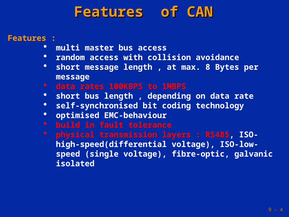
Features of CANFeatures of CAN
Features : multi master bus access random access with collision avoidance short message length , at max. 8 Bytes per message data rates 100KBPS to 1MBPS short bus length , depending on data rate self-synchronised bit coding technology optimised EMC-behaviour build in fault tolerance physical transmission layers : RS485, ISO-high-
Implementation / Classification of CANImplementation / Classification of CAN The Implementation of CAN in Silicon
Don’t get confused !
Communication is identical for all implementations of CAN. However, there are two principal hardware implementations and two additional versions of data formats :
CAN-Implementation
Full-CANBASIC-CAN
9 - 9 - 88
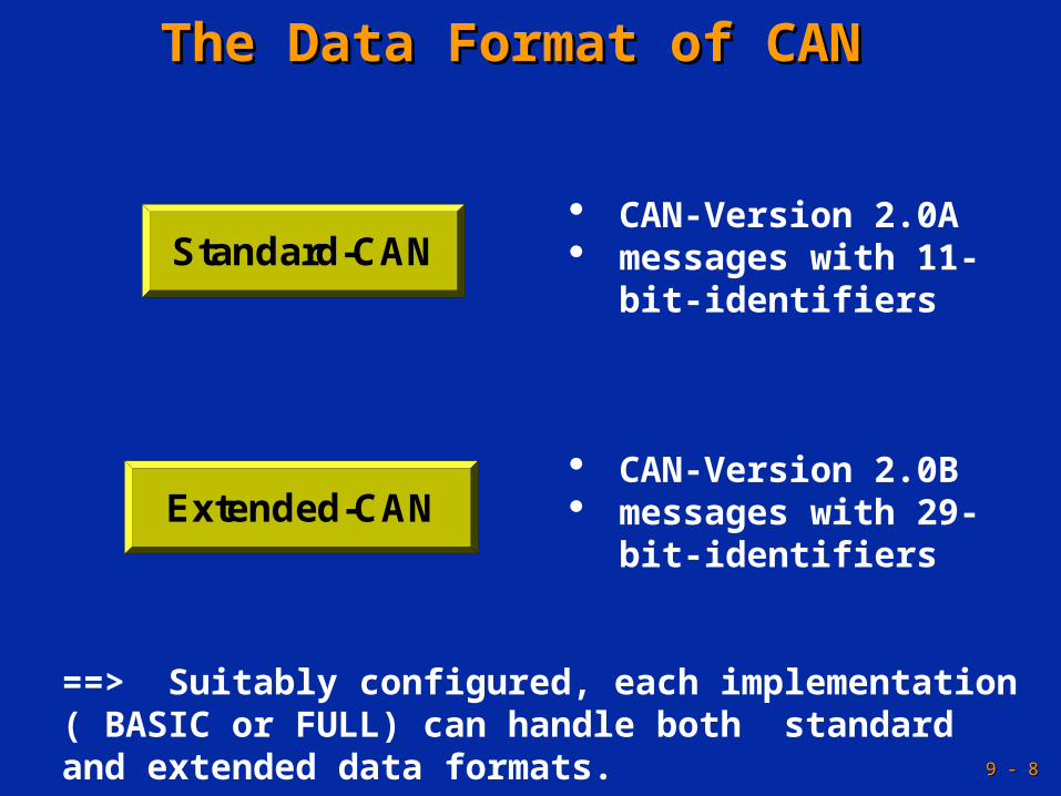
The Data Format of CAN The Data Format of CAN
CAN-Version 2.0A messages with 11-bit-
identifiers
CAN-Version 2.0B messages with 29-bit-
identifiers
==> Suitably configured, each implementation ( BASIC or FULL) can handle both standard and extended data formats.
Standard-CAN
Extended-CAN
9 - 9 - 99
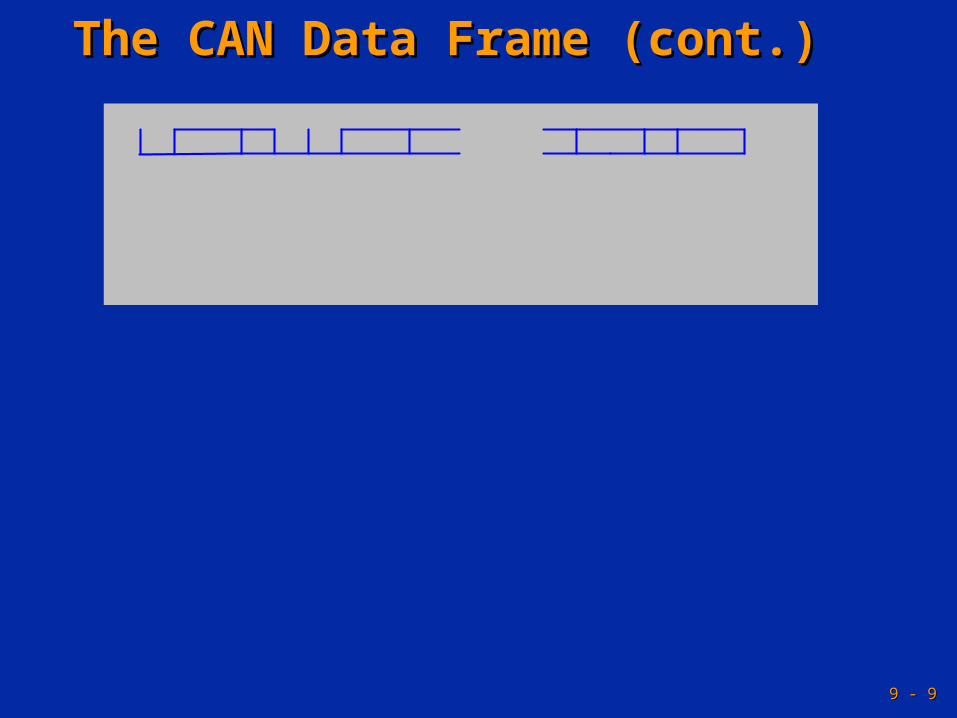
The CAN Data Frame (cont.) The CAN Data Frame (cont.)
EOF + IFS10 bits
ACK2 bits
CRC15 bits
data0...8 byte
DLC4 bits
r01 bit
IDE1 bit
RTR1bit
Identifier11 bits
start1 bit
Identifier11 bits
start1 bit EOF + IFS
10 bits
ACK2 bits
CRC15 bits
data0...8 byte
DLC4 bits
r01 bit
r11bit
RTR1bitSRR
1bit
IDE1bit
Identifier18bit
DATA-Frame CAN 2.0A ( 11-bit-identifier )
DATA-Frame CAN 2.0B ( 29-bit-identifier )
9 - 9 - 1010
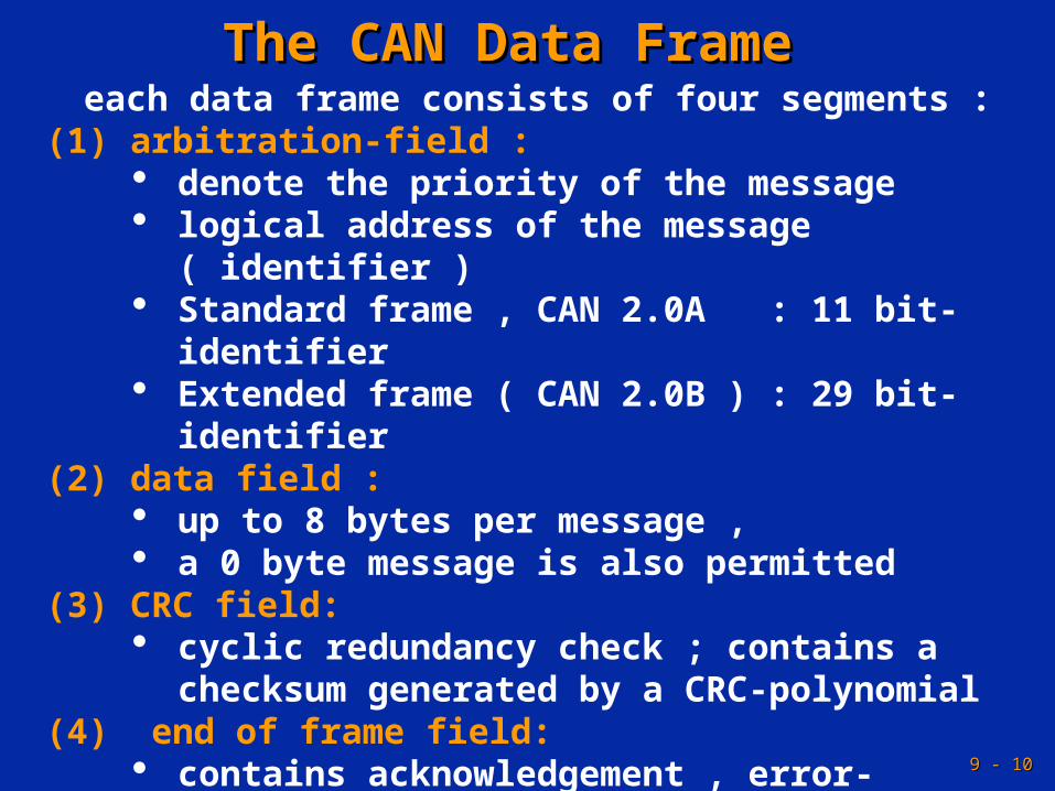
The CAN Data Frame The CAN Data Frame each data frame consists of four segments :
(1) arbitration-field : denote the priority of the message logical address of the message ( identifier ) Standard frame , CAN 2.0A : 11 bit-identifier Extended frame ( CAN 2.0B ) : 29 bit-identifier
(2) data field : up to 8 bytes per message , a 0 byte message is also permitted
(3) CRC field: cyclic redundancy check ; contains a checksum
generated by a CRC-polynomial(4) end of frame field:
contains acknowledgement , error-messages, end of message
9 - 9 - 1111
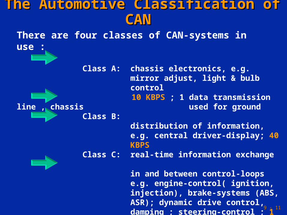
The Automotive Classification of CAN The Automotive Classification of CAN
There are four classes of CAN-systems in use :
Class A: chassis electronics, e.g. mirror adjust, light & bulb control10 KBPS ; 1 data transmission line ,
chassis used for groundClass B: distribution of information, e.g. central
driver-display; 40 KBPSClass C: real-time information exchange
in and between control-loops e.g. engine-control( ignition, injection), brake-systems (ABS, ASR); dynamic drive control, damping ; steering-control ; 1 MBPS
Class D: network with large number of data’s ( > 10KB/frame) , e.g. radio, telephone, navigation-systems
9 - 9 - 1212
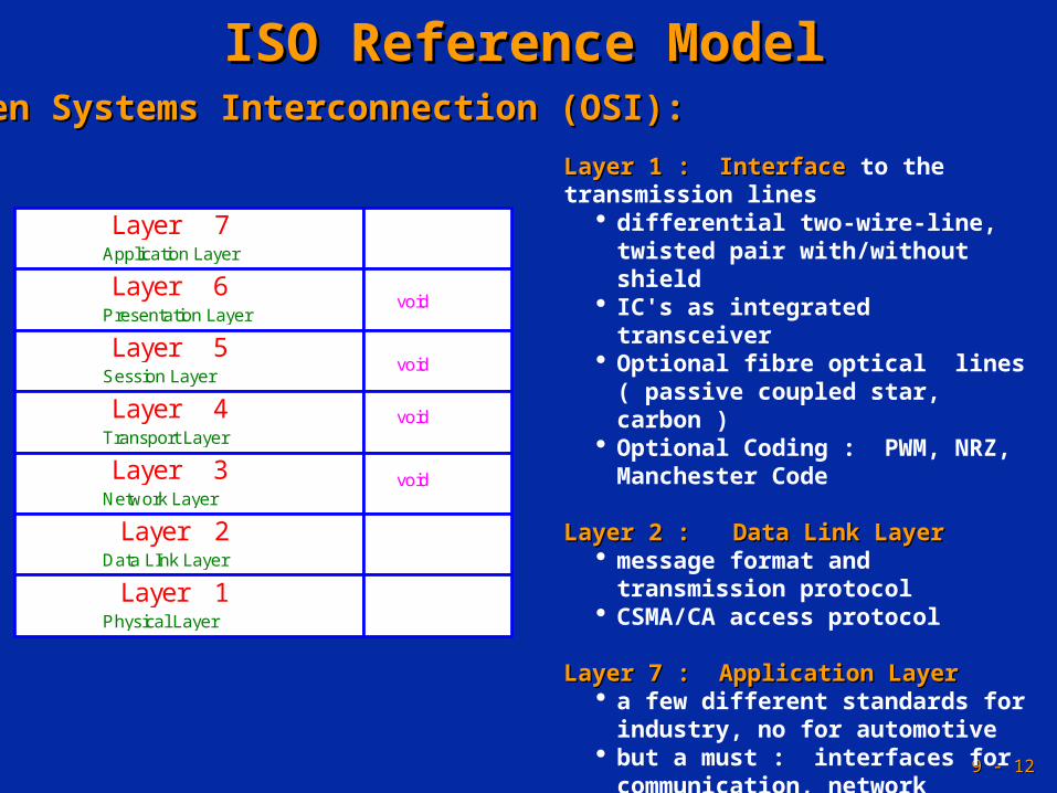
ISO Reference ModelISO Reference ModelOpen Systems Interconnection (OSI):Open Systems Interconnection (OSI):
Layer 7
Layer 6
Layer 5
Layer 4
Layer 3
Layer 2
Layer 1
Application Layer
Presentation Layer
Session Layer
Transport Layer
Network Layer
Data LInk Layer
Physical Layer
void
void
void
void
Layer 1Layer 1 :: InterfaceInterface to the transmission lines differential two-wire-line, twisted pair
CAN Access Procedure: CSMA/CACAN Access Procedure: CSMA/CA
node A
node B
bus line
Tx
Rx
Tx
Rx
start id10id9
id8 id7id6
CSMA/ CA = Carrier Sense Multiple Access with Collision Avoidance
access-control with non destructive bit-wide arbitration
if there is a collision , ”the winner takes the bus”
the message with higher priority is not delayed !
real-time capability for high prioritised messages
the lower the identifier, the higher the priority
9 - 9 - 1515
CSMA/CA (cont.)CSMA/CA (cont.)CSMA / CA =CSMA / CA ="bit - wide arbitration during transmission with simultaneous receiving and comparing of the transmitted message" means :
• if there is a collision within the arbitration-field, only the node with the lower priority cancels its transmission.
• The node with the highest priority continues with the transmission of the message.
node 1 node 2 node 3
high : reccessive
low : dominant
node 1 node 2 node 3 bus high high high high high low high low low low high low
Vcc
R
9 - 9 - 1616
CAN Physical LayersCAN Physical LayersCAN - High - Speed ( ISO 11898 ) :CAN - High - Speed ( ISO 11898 ) :
node 1 node 30
120
Ohm120
Ohm
CAN_H
CAN_L
Voltage
time
2,5V
3,5V
1,5V
CAN_H
CAN_L
recessive dominant recessicve
CAN high-speed , nominal bus levels
9 - 9 - 1717
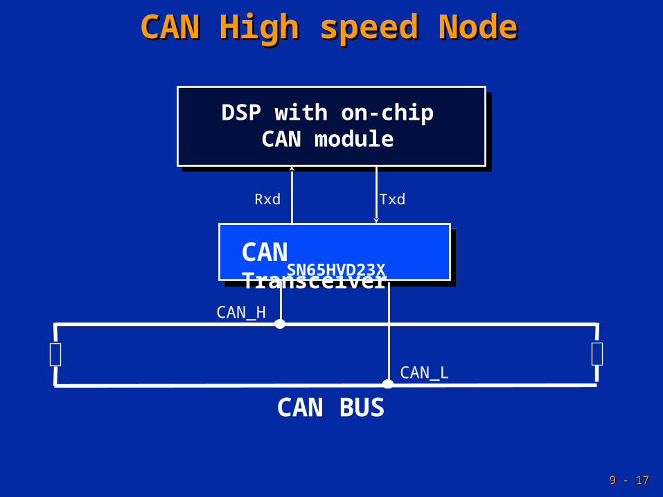
CAN High speed NodeCAN High speed Node
DSP with on-chipCAN module
CAN Transceiver
CAN BUS
TxdRxd
CAN_L
CAN_H
SN65HVD23X
9 - 9 - 1818
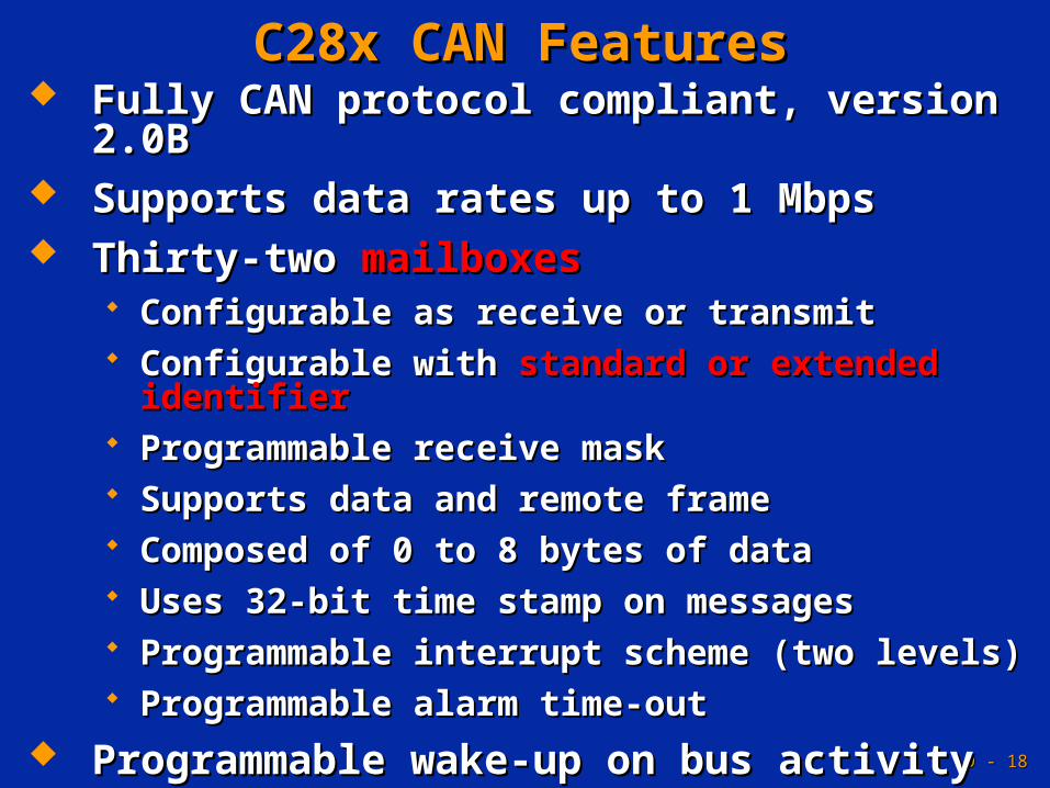
C28x CAN FeaturesC28x CAN Features Fully CAN protocol compliant, version 2.0BFully CAN protocol compliant, version 2.0B Supports data rates up to 1 MbpsSupports data rates up to 1 Mbps Thirty-two Thirty-two mailboxesmailboxes
Configurable as receive or transmitConfigurable as receive or transmit Configurable with Configurable with standard or extended identifierstandard or extended identifier Programmable receive maskProgrammable receive mask Supports data and remote frameSupports data and remote frame Composed of 0 to 8 bytes of dataComposed of 0 to 8 bytes of data Uses 32-bit time stamp on messagesUses 32-bit time stamp on messages Programmable interrupt scheme (two levels)Programmable interrupt scheme (two levels) Programmable alarm time-outProgrammable alarm time-out
Programmable wake-up on bus activityProgrammable wake-up on bus activity Self-test mode Self-test mode
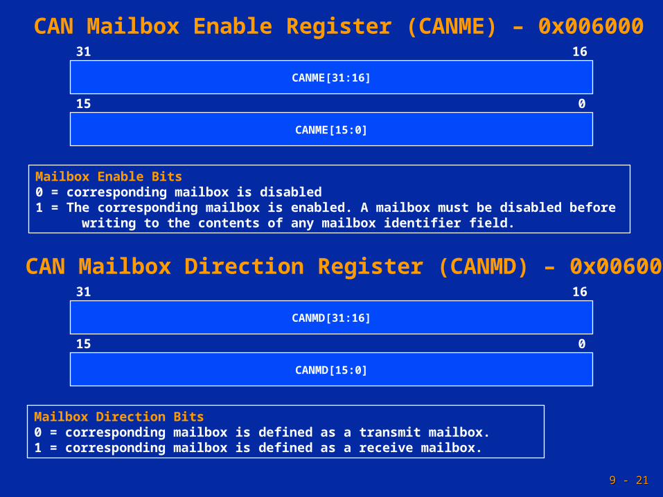
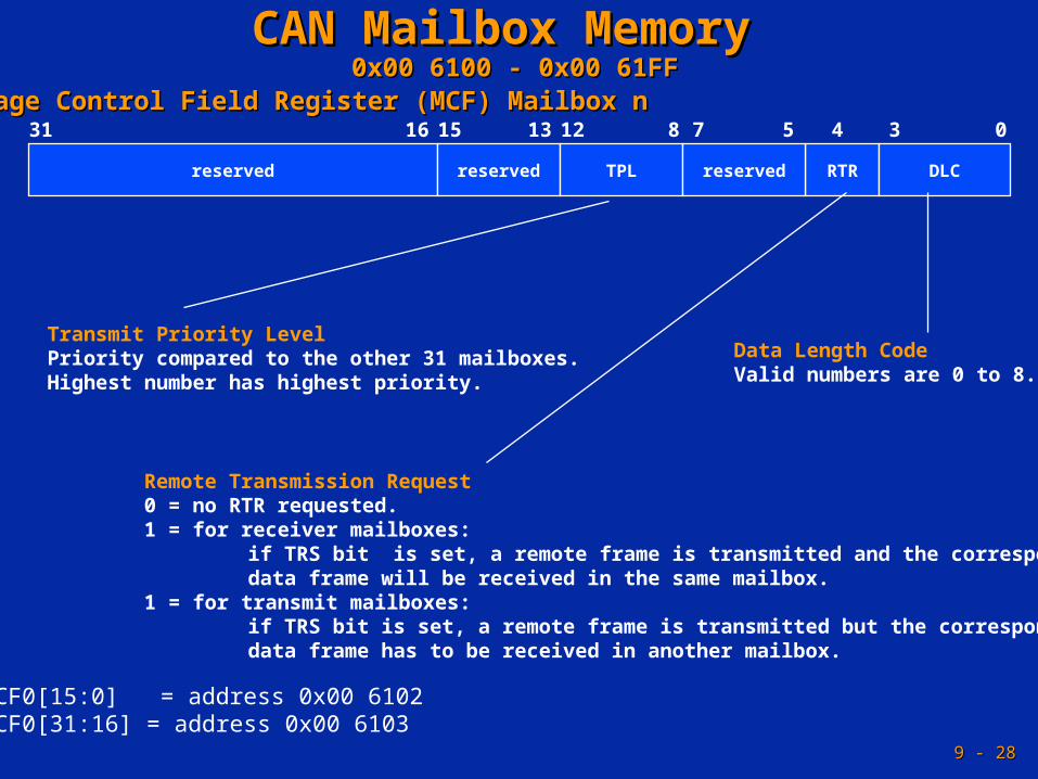
Mailbox Enable Bits0 = corresponding mailbox is disabled1 = The corresponding mailbox is enabled. A mailbox must be disabled before writing to the contents of any mailbox identifier field.
CAN Mailbox Direction Register (CANMD) – 0x006002
15
1631
CANMD[15:0]
CANMD[31:16]
0
Mailbox Direction Bits0 = corresponding mailbox is defined as a transmit mailbox.1 = corresponding mailbox is defined as a receive mailbox.
9 - 9 - 2222
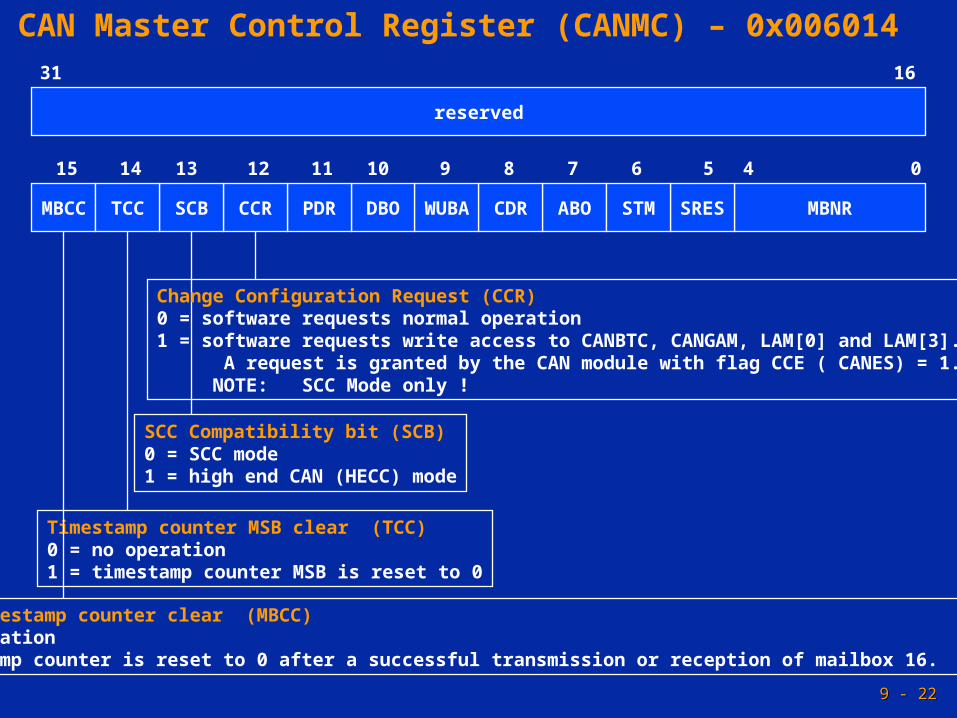
CAN Master Control Register (CANMC) – 0x006014
15
1631
reserved
0
MBCC MBNR
Mailbox Timestamp counter clear (MBCC)0 = no operation 1 = timestamp counter is reset to 0 after a successful transmission or reception of mailbox 16.
ABOCDRWUBADBOPDRCCRSCBTCC SRESSTM
414 13 12 11 10 9 8 7 6 5
Timestamp counter MSB clear (TCC)0 = no operation 1 = timestamp counter MSB is reset to 0
SCC Compatibility bit (SCB)0 = SCC mode 1 = high end CAN (HECC) mode
Change Configuration Request (CCR)0 = software requests normal operation 1 = software requests write access to CANBTC, CANGAM, LAM[0] and LAM[3]. A request is granted by the CAN module with flag CCE ( CANES) = 1. NOTE: SCC Mode only !
9 - 9 - 2323
CAN Master Control Register (CANMC) – 0x006014 (cont.)
15 0
MBCC MBNRABOCDRWUBADBOPDRCCRSCBTCC SRESSTM
414 13 12 11 10 9 8 7 6 5
Data Byte Order (DBO) in Mailbox RegistersMDH[31:0] and MDL[31:0]0 = MDH[31:0] : Byte 4,5,6,7 ; MDL[31:0] : Byte 0,1,2,3 1 = MDH[31:0] : Byte 7,6,5,4 ; MDL[31:0] : Byte 3,2,1,0
Wake up on bus activity (WUBA)0 = Module leaves power down only after writing a 0 to PDR 1 = Module leaves power down on any bus activity
Change data field request (CDR)0 = normal operation 1 = software requests access to the data field in 2MBNR”. NOTE: software must clear this bit after access is done.
Auto bus on (ABO)0 = “bus off’ state is permanent. 1 = “bus off” state is left into “bus on” after 128*11 recessive bits have been received.
Self Test Mode (STM)0 = normal mode 1 = Module generates its own ACK
Software Reset(SRES)0 = no effect 1 = CAN Module reset
Mailbox Number(MBNR)Number , used for CDR
Power Down Mode Request (PDR)0 = normal operation 1 = power down mode is requested.NOTE: bit is automatically cleared upon wakeup from power down!
9 - 9 - 2424
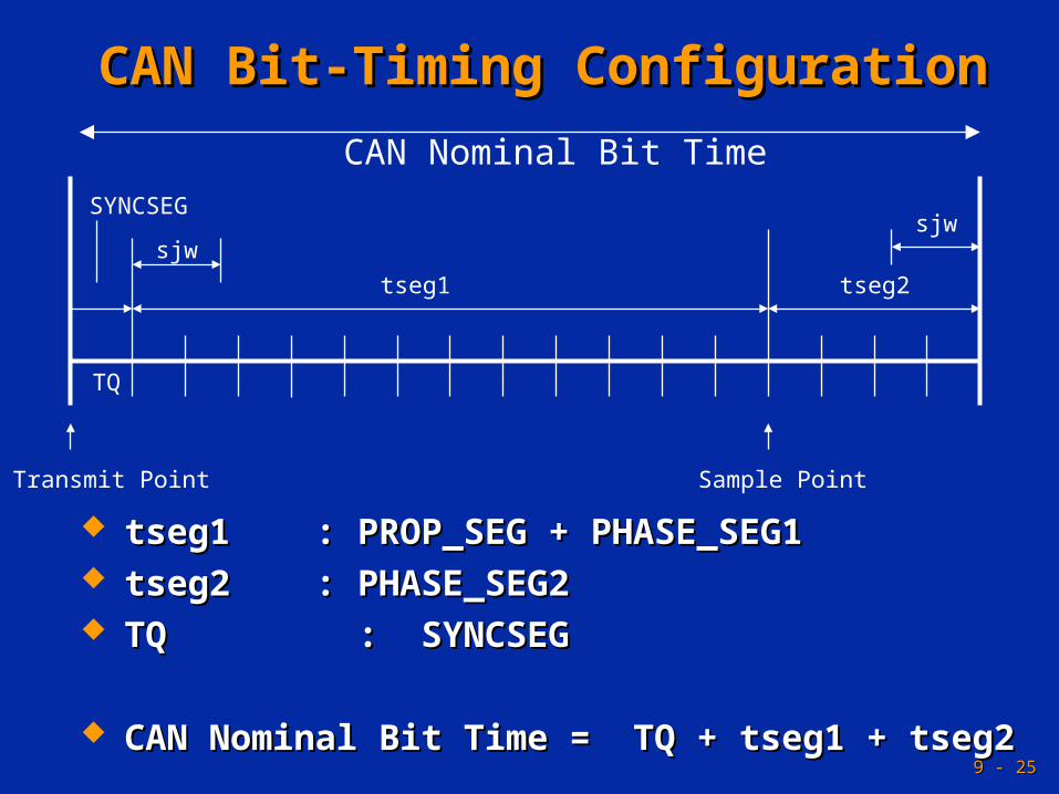
CAN Bit-Timing ConfigurationCAN Bit-Timing Configuration CAN protocol specification splits the nominal bit CAN protocol specification splits the nominal bit
time into four different time segments:time into four different time segments: SYNC_SEGSYNC_SEG
Used to synchronize nodesUsed to synchronize nodes Length : always 1 Time Quantum (TQ)Length : always 1 Time Quantum (TQ)
PROP_SEGPROP_SEG Compensation time for the physical delay times within the netCompensation time for the physical delay times within the net Twice the sum of the signal’s propagation time on the bus line, the input Twice the sum of the signal’s propagation time on the bus line, the input
comparator delay and the output driver delay.comparator delay and the output driver delay. Programmable from 1 to 8 TQProgrammable from 1 to 8 TQ
PHASE_SEG1PHASE_SEG1 Compensation for positive edge phase shiftCompensation for positive edge phase shift Programmable from 1 to 8 TQProgrammable from 1 to 8 TQ
PHASE_SEG2PHASE_SEG2 Compensation time for negative edge phase shiftCompensation time for negative edge phase shift Programmable from 2 to 8 TQProgrammable from 2 to 8 TQ
9 - 9 - 2525
CAN Bit-Timing ConfigurationCAN Bit-Timing Configuration
Acceptance Mask Enable Bit ( receiver only)0 = no Acceptance Mask used. All identifier bits must match to receive the message1 = the corresponding Acceptance Mask is used)
Auto Answer Mode Bit ( transmitter only)0 = mailbox does not reply to remote requests.1 = if a matching Remote Request is received, the contents of this mailbox will be sent.
Message IdentifierStandard Frames : IDn[28:18] are usedExtended Frames : IDn[28:0] are used
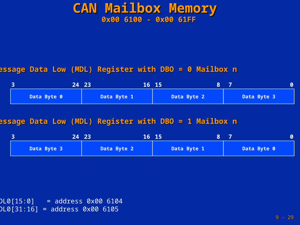
Message Data High (MDH) Register with DBO = 1 Mailbox nMessage Data High (MDH) Register with DBO = 1 Mailbox n
16 8 7
Data Byte 6 Data Byte 4Data Byte 5
9 - 9 - 3131
CAN Example : transmit a frameCAN Example : transmit a frame Lab 9: Transmit a CAN message
CAN baud rate : 100 KBPS ( CAN low speed ) Transmit a one byte message every second Message Identifier 0x 1000 0000 ( extended frame) Use Mailbox #5 as transmit mailbox Message content: status of the input switches
( GPIO B15-B8) CAN transceiver SN 65 HVD 230 ( Zwickau Adapter
Board) : Set jumper JP5 and JP6 to 1-2 Set jumper JP4 to 2-3 ( enables on board line
terminator of 120 Ohm) DB9 (male) to connect the Adapter Board to CAN
Pin 2 : CAN_L ; Pin 7 : CAN_H ; Pin 3 : GND
9 - 9 - 3232
CAN Example : receive a frameCAN Example : receive a frame Lab 10: Receive a CAN message
CAN baud rate : 100 KBPS ( can low speed ) Receive a one byte message and show it on GPIO-
Port B7…B0 ( 8 LED’s) Message Identifier 0x 1000 0000 ( extended frame) Use Mailbox #1 as receive mailbox CAN Transceiver SN 65 HVD 230 ( Zwickau
Adapter Board) : Set jumper JP5 and JP6 to 1-2 Set jumper JP4 to 2-3 ( enables on board line
terminator of 120 Ohm) DB9 (male) to connect the Adapter Board to CAN


![Retriggerable Monostable Multivibrators€¦ · Retriggerable Monostable Multivibrators Author: Texas Instruments, Incorporated [SDLS043,*] Subject: Data Sheet Keywords: SDLS043 Created](https://static.documents.pub/doc/80x56/605c572698fa48206917a2eb/retriggerable-monostable-multivibrators-retriggerable-monostable-multivibrators.jpg)