26
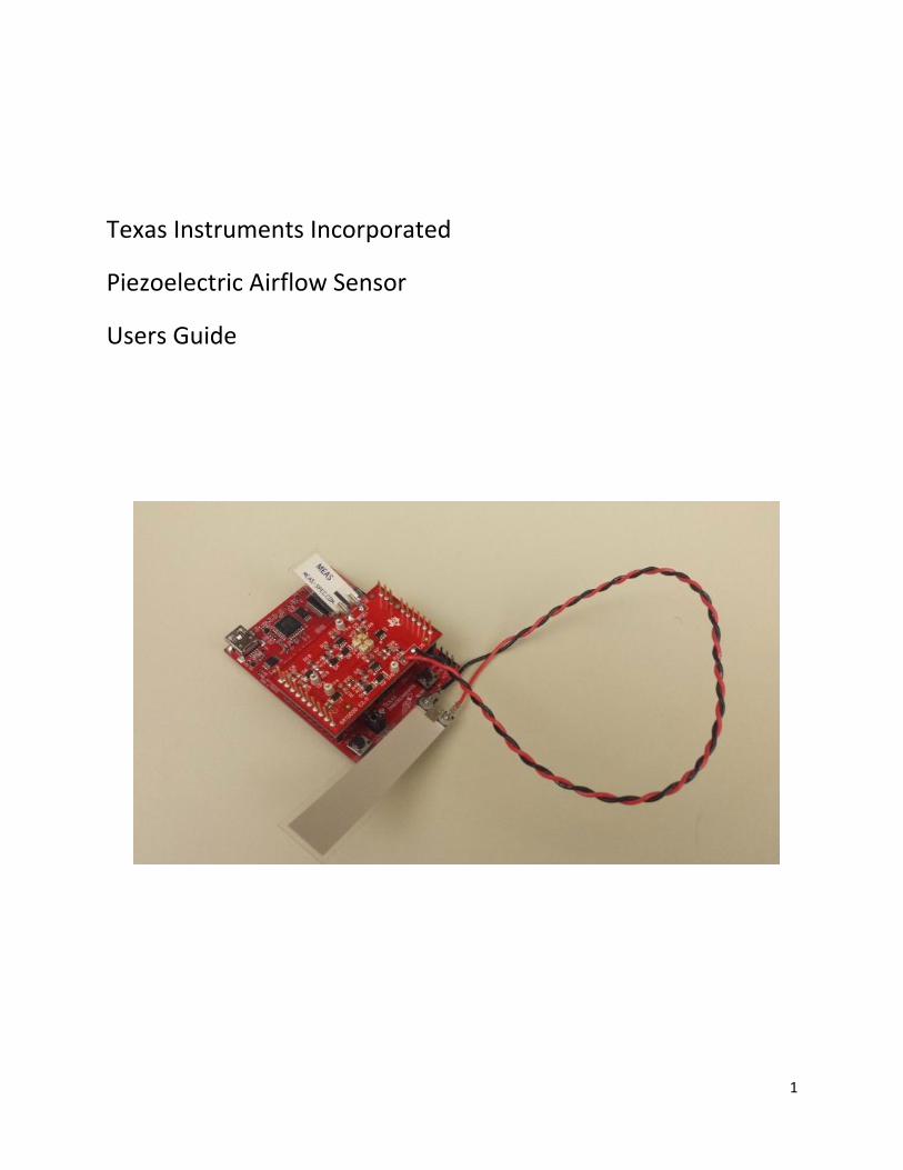
1 Texas Instruments Incorporated Piezoelectric Airflow Sensor Users Guide
| Date post: | 04-Jun-2018 |
| Category: |
Documents |
| Upload: | nguyenminh |
| View: | 218 times |
| Download: | 1 times |
1
Texas Instruments Incorporated
Piezoelectric Airflow Sensor
Users Guide

2
Table of Contents
Design Goals .................................................................................................................................................. 3
Features ........................................................................................................................................................ 3
Piezoelectric Air Flow Features ..................................................................................................................... 3
TI Part Number Features ............................................................................................................................... 3
Featured Applications ................................................................................................................................... 4
Highlighted Products ..................................................................................................................................... 4
Block Diagram ............................................................................................................................................... 5
Hardware Description ................................................................................................................................... 6
Getting Started: What's Needed ................................................................................................................... 6
Functional Test Information.......................................................................................................................... 8
Test Setup .................................................................................................................................................... 8
Test Considerations..................................................................................................................................... 11
Test Results ................................................................................................................................................. 13
EVM Design Considerations and Simulations ............................................................................................. 17
Simulations .................................................................................................................................................. 19
Design Optimizations .................................................................................................................................. 22
Final Conclusions ........................................................................................................................................ 24
References Section ..................................................................................................................................... 25
3
Design Goals
To understand the design it is important to understand the conditions we began with as well as the goal of the design. The overarching goal is to create a simple solution to detect airflow and trigger an alarm or indicate to a user when it has stopped. We had some initial specific design requirements:
Use a Piezoelectric sensing element which can be either board mounted or remote. We chose to use sensors from the DT Series by Measurement Specialties. We want to fit multiple channels on the board if possible.
Work with the MSP430 Launchpad and its integrated ADC as the "signal processor." This necessitates using the BoosterPack form factor
Operate off of the Launchpad's power, so we are limited to a single 3.3V power rail. This also means our ADC will be using this as a reference.
Need visual way to see the output of the circuit Detect a lack of airflow within a few seconds of the source being removed, and avoid
false alarms Minimize the cost and size of the solution
The above few requirements actually leave the design rather open, but gave us a good point to begin with.
Features
Piezoelectric Air Flow Features
MSP430 LaunchPad BoosterPack form factor Reference design for customers wishing to incorporate piezoelectric airflow sensing into
their systems
TI Part Number Features
MSP-EXP430G2 o 14-/20-pin DIP (N) socket o Built-in flash emulation for debugging and programming o 2 programmable LEDs o 1 power LED o 1 programmable button o 1 reset button o Features MSP430G2553 Value-Line low-power microcontroller

4
OPA2337 o Channels: 2 o Supply Voltage: 2.7 V to 5.5 V o Quiescent Current: 525 µA (typ) o Bandwidth: 3 MHz o Slew Rate: 1.2 V/µs o Settling Time: 2 µs (2VSTEP) o Overdrive Recovery Time: 2 µs o THD: 0.001% at 1 kHz o Input Bias Current: 10pA (max) o Input Voltage Noise Density: 26 nV/rtHz (f = 1 kHz) o Input Offset Voltage: 500 µV (3 mV max) o CMRR: 74 dB o RRO – Rail-to-Rail Output o Operating Temperature Range: –40°C–85°C
Featured Applications
The Piezoelectric Airflow Sensor was designed to demonstrate how a piezoelectric film sensor can be used in conjunction with an MSP430 microcontroller to provide a low-cost solution to detecting the presence or absence of fan airflow:
Server exhaust airflow detection Desktop computer exhaust airflow detection
Highlighted Products
The Platform features the following device:
OPA2337 - Dual-channel, Single Supply, CMOS Amplifier MSP430G2553 - Low-cost, Ultra Low Power 16-bit Microcontroller

5
Block Diagram

6
Hardware Description
Getting Started: What's Needed
MSP430 LaunchPad with MSP430G2553 Code Composer Studio to load firmware onto the MSP430G2553 Piezoelectric Airflow Sensor BoosterPack Windows GUI (optional)
Easy Steps to Get Going
Typical configuration of the module is as follows:
Step 1:
Plug Piezoelectric Airflow Sensor BoosterPack into MSP430 LaunchPad, as pictured below.

7
Step 2:
Load firmware onto MSP430 LaunchPad using Code Composer Studio v5.4 or later
Step 3:
Run Piezoelectric Airflow Sensor GUI program Choose proper COM port, corresponding to MSP430 LaunchPad UART module
o Check using Windows Device Manager -> Ports Observe signal on GUI, as well as red & green LEDs on LaunchPad
o Red LED indicates insufficient airflow detected o Green LED indicates good airflow detected

8
Functional Test Information
Test Setup
The Piezoelectric Airflow Sensor was tested first in a makeshift "wind tunnel" in direct airflow from a variable speed PC fan (4", variable voltage up to 12V). The PVC pipes serves to shield disturbances from the airflow in the room. It also better conditions the airflow to simulate the tight dimensions of a server. In the picture below, the 4" fan is mounted on the left end of a 2'x4" PVC pipe, and the sensor is inserted in the right end.
Test set up. The airflow sensor is "mounted" inside the PVC wind tunnel with a clamp.

9
Looking down the wind tunnel from the perspective of the fan.
We also used an anemometer (airflow meter) to roughly measure the airspeed at different settings of the PC fan for reference. You can see the anemometer setup in the picture below. It should be noted that since we are working with relatively low air speeds and in a tight flow cross section, the measurement is very rough and depends on the orientation of the probe and where in the PVC the flow was measured.

10
Image showing the use of the anemometer to measure air flow speeds.

11
Test Considerations
Several things need to be noted about the test set-up.
First of all, the positioning and mounting of the airflow sensor itself (the piezo element) is extremely critical to the test output in several ways that were observed during testing:
The airspeed seemed to be higher locally around the edges of the 'wind tunnel' and calmer in the center. This is most likely due to the fact that the airflow is more turbulent at the edges and indicates that, in an end application, the presence of other objects around the sensor can affect how relatively sensitive it is to the "same" airflow. For our testing we found placing the sensor near the sides of the PVC gave best results for the sensitivity of our particular sensor element.
The orientation of the sensor with respect to the airflow is very important. On the left of the image below you can see 3 ways in which the airflow could hit the sensor; either on-edge to the length (red), on-edge to the width (blue), or catching it broad-side (green). We found that the blue option seems to be the best, with the sensor just slightly askew from being directly on-edge. The red option gave good sensitivity but a less consistent amplitude/frequency. The green option was very poor in low conditions and almost no response except when the airflow was quite high. All tests performed below were done with the 'blue' option.

12
The way that the sensor is mounted was quite important to the sensitivity. On the right side of the picture above there are 3 different arrows indicating different options for where to "hold" the sensor; held by the wires near the sensor element, held just on the edge of the sensor laminate material, and held on the sensor element itself. The main affect of this is affecting the rigidity of the sensor and therefore the level of airflow it is sensitive to: the less rigidly held, lower airspeeds gave good response, but not at higher speeds. The opposite is true for more rigid sensors. The length of the sensor used is actually also very important; the longer the sensor, the more responsive it is to low air speed. The sensor we used was ~3" long and best results were found by mounting it just on the edge of the laminate material. In our testing, almost no response is seen when using very short sensors, especially when board-mounted, or longer sensors 'choked' by mounting them further up the sensor element.
13
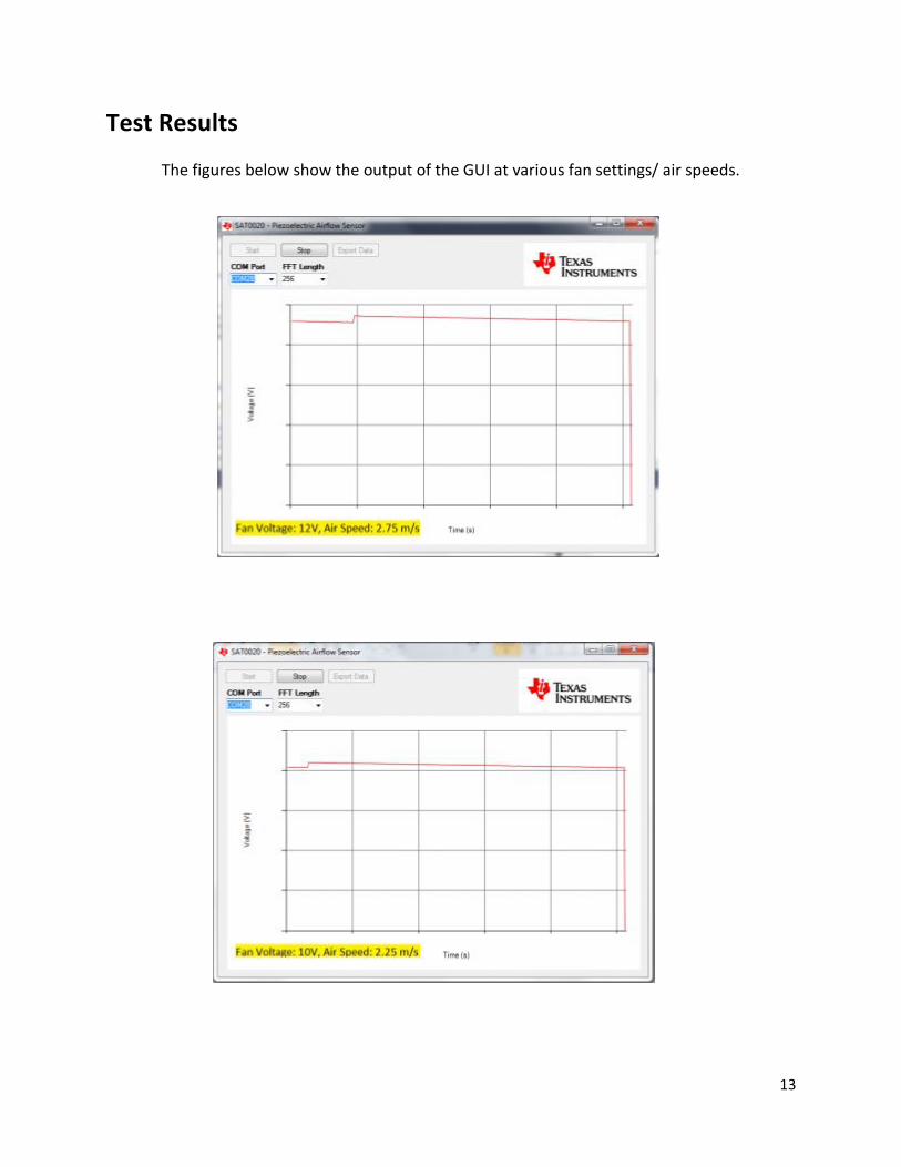
Test Results
The figures below show the output of the GUI at various fan settings/ air speeds.

14

15
GUI output of piezo sensor exposed to different air speeds. Note that the GUI is scaled for 0-
>3.3V although the operational range is just 1.65->3.3V.
16
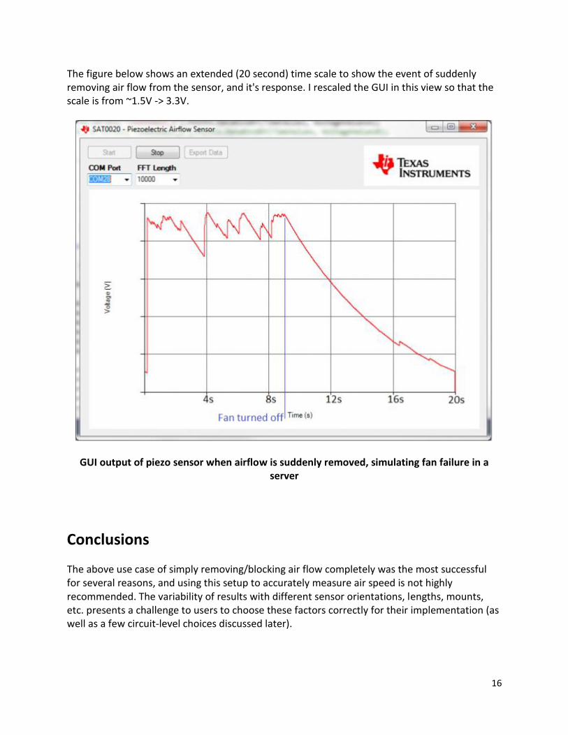
The figure below shows an extended (20 second) time scale to show the event of suddenly removing air flow from the sensor, and it's response. I rescaled the GUI in this view so that the scale is from ~1.5V -> 3.3V.
GUI output of piezo sensor when airflow is suddenly removed, simulating fan failure in a server
Conclusions
The above use case of simply removing/blocking air flow completely was the most successful for several reasons, and using this setup to accurately measure air speed is not highly recommended. The variability of results with different sensor orientations, lengths, mounts, etc. presents a challenge to users to choose these factors correctly for their implementation (as well as a few circuit-level choices discussed later).
17
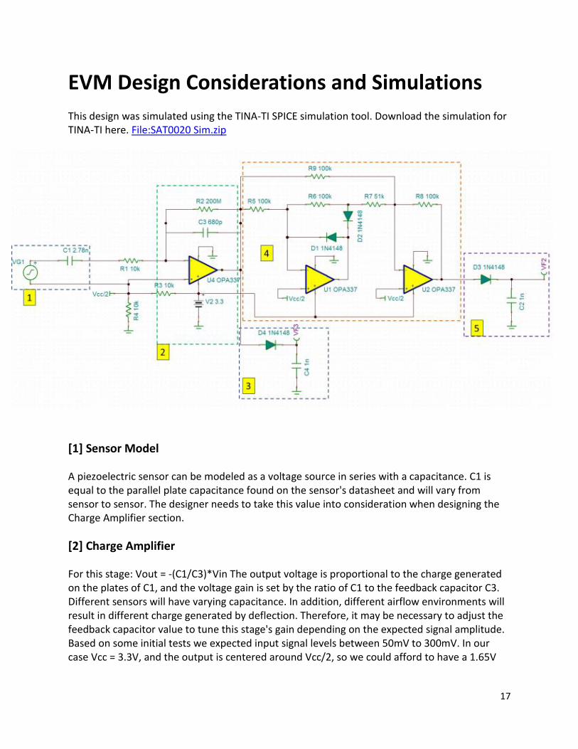
EVM Design Considerations and Simulations
This design was simulated using the TINA-TI SPICE simulation tool. Download the simulation for TINA-TI here. File:SAT0020 Sim.zip
[1] Sensor Model
A piezoelectric sensor can be modeled as a voltage source in series with a capacitance. C1 is equal to the parallel plate capacitance found on the sensor's datasheet and will vary from sensor to sensor. The designer needs to take this value into consideration when designing the Charge Amplifier section.
[2] Charge Amplifier
For this stage: Vout = -(C1/C3)*Vin The output voltage is proportional to the charge generated on the plates of C1, and the voltage gain is set by the ratio of C1 to the feedback capacitor C3. Different sensors will have varying capacitance. In addition, different airflow environments will result in different charge generated by deflection. Therefore, it may be necessary to adjust the feedback capacitor value to tune this stage's gain depending on the expected signal amplitude. Based on some initial tests we expected input signal levels between 50mV to 300mV. In our case Vcc = 3.3V, and the output is centered around Vcc/2, so we could afford to have a 1.65V

18
swing before clipping the signal. We chose to go with a gain of 4, a maximum swing of 1.2V or 2.4V peak-to-peak, which fits into our desired range with some overhead left over.
As charge is generated on C1 (the sensor), it will transfer to C3 and begin to build there. Without R2 this would quickly lead to the capacitor fully charging and the amplifier would drift into saturation. R2 slowly bleeds the charge off of the capacitor to prevent this. The combination of C3 and R2 in the feedback network also create a high-pass filter on the incoming signal. The corner frequency of this filter should be set very low since we are working with low frequencies.
The last thing to consider is that R2 will provide a DC bias path for the input bias current, and will create an offset of V_offset = I_bias * R2. This is why it is important to choose an opamp with very low input bias current.
[3] Half-wave Rectification & Smoothing
On the physical board, this is actually not present and is just used for simulation. Instead of a separate diode & cap, there is an option to route the output of the Charge Amplifier directly to block 5, which we discuss below.
[4]&[5] Absolute Value circuit and smoothing
For the absolute value stage: Vout = abs(Vin) [Unity gain] Since our goal is to produce a quasi-DC signal from the input, the first step will be rectification. This is an "Absolute Value" circuit which does full-wave rectification of the input signal to produce an output which is all greater than the offset voltage. See the simulations below for an example of the output at this stage.
The resistors used for R5-R9 should be 1% tolerance. This is to leave the gain unaffected, as well as to ensure that both the positive and negative inputs are rectified equally. If R9 and R6 differ in value, this will be seen on the output as every other peak being lower than the others. Small tolerance resistors help maintain symmetry.
The output diode and capacitor serve to smooth the output and provide as close to a DC signal as possible for reading by the ADC. The actual output will not be as smooth as the simulations show due to the sporadic nature of the input signal, however.
19
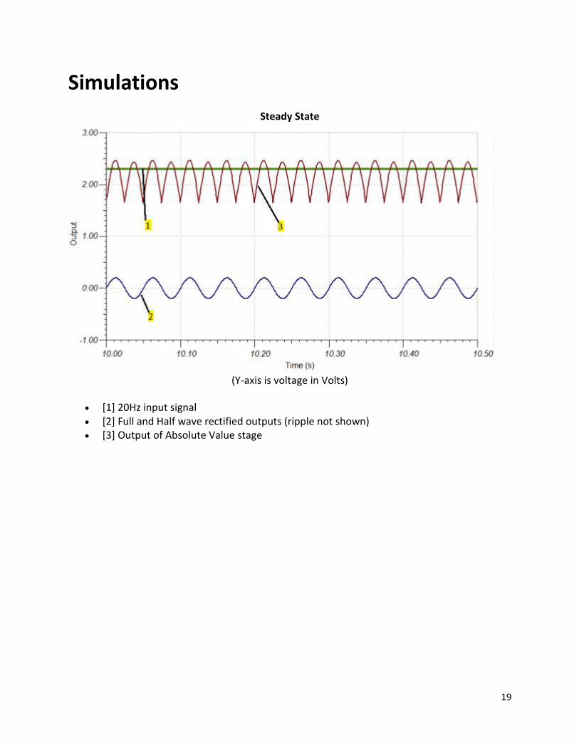
Simulations
Steady State
(Y-axis is voltage in Volts)
[1] 20Hz input signal [2] Full and Half wave rectified outputs (ripple not shown) [3] Output of Absolute Value stage

20
Starting Behavior
(Y-axis is voltage in Volts)
[1] 100Hz input signal (modeling sensor input) [2] Full-wave rectified output [3] Half-wave rectified output
It is not immediately clear from this image, but the ripple voltage of the half-wave rectified output is obviously 2x of the full-wave. The choice between the two depends on the level of accuracy needed.

21
[1] Red, frequency response of the half-wave rectified output [2] Green, frequency response of the full-wave rectified output
Design Errors
If using board version SAT0020 E2.0, pin 17 of the Launchpad has been mistakenly grounded by the BoosterPack. This prevents the MSP430 from being programmed while the BoosterPack is plugged in as it grounds the JTAG TEST pin. A simple workaround is either to clip the pin from the header on the launchpad (it's only function is TEST which is not required on the Boosterpack), or simply program the device with the BoosterPack unplugged.
This error has been corrected in rev E2.1, which is the version who's design files are presented here.

22
Design Optimizations
Alternate Parts
Here are some alternative part numbers to the OPA2337.
IVC102 - Precision Switched Integrator Transimpedance Amplifier o Pros
This amplifier is similar to the OPA337/OPA2337 in that it has extremely low bias current, which is very important for the Charge Amplifier stage (1st stage) of our circuit
The device has some integrated feedback capacitors and thus reduces the number of components needed and saves the cost of external passive resistors and capacitors
o Cons This part is a significant price increase over the OPA337/OPA2337, and is
a bit more complicated to use The IVC part only comes in a single-channel, 14-pin SOIC package, and is
therefore unlikely to save any board space
LMV772 - Dual Channel Low offset, Low Noise Amplifier o Pros
Lower Bias Current, Offset, and Voltage noise than the OPA2337 Also available in quad channel package (LMV774)
o Cons More expensive than the OPA337 Poorer CMRR than OPA337
LMP7702MM - Dual Channel Precision Amplifier o Pros
Lower Bias Current, Offset, and Voltage noise than the OPA2337 Huge improvement in CMRR as compared to other alternatives Also available in quad channel package (LMV774)
o Cons Larger package than OPA337 or LMV772 More expensive than the OPA337
Output Configurations
There are three ways in which the output of the first amplifier stage can be monitored, each offering its own set of advantages
Full rectification and filtering using precision Absolute Value circuit
23
o This configuration uses dual OPA337s to translate the output of the charge amplifier to a DC value which corresponds to the peak amplitude of the input signal. The action of the amplifiers corrects for the diode drops associated with rectification. Using high-precision feedback resistors allows for a highly accurate output
o The absolute value circuit has the highest component count of all three options, however it has the most precise output and requires little signal processing to interpret (aside from averaging)
o This is selectable via a 0 ohm resistor on the SAT0020 board (populate R18/R20 and depopulate R19/R17)
Half-wave rectification and filtering o This configuration uses only a diode and an output capacitor to rectify and
smooth the output of the charge amplifier. Like the absolute-value circuit, it will be read by the MSP430 as a DC value and therefore requires very little signal processing (averaging is still done in the example code)
o This option requires very few components, only one rectifying diode and an output filter
o For a perfect sine wave this will have about 2x the ripple voltage on the output as compared to the absolute-value circuit. However, the output of the sensor is much more sporadic and not guaranteed to be symmetric between it's positive and negative outputs (this depends on the way in which the sensor is deflected). Since the half-wave rectification will essentially block half of the incoming signal, it's possible that the final output won't be completely representative of the sensor signal.
o This configuration is selectable via a 0 ohm resistor on the SAT0020 board (populate R19/R17 and depopulate R18/R20)
Direct output from the charge amplifier o This configuration requires no additional components past the charge amplifier
(first stage) o The MSP430 will need to do "peak detection" and some averaging to get use out
of this signal. However, since this configuration can feed the "raw" data to the PC, there is the opportunity to have access to the frequency content of the incoming signal, which is lost in the other two configurations.
o Due to the overhead of the signal processing, this configuration does not scale as well to multiple sensors as the other two configurations
o This signal is available via headers (J3 and J4) on the SAT0020 and the user has the option to feed this to open analog channels on the MSP430 via jumper wire

24
Output Capacitor Sizing
The value of the output capacitor (or "smoothing capacitor"), C2/C4 in the simulation above, can be important to the final implementation of this design. It becomes especially important in the use case where the user simply wants to detect the absence of airflow. The value of the capacitor will affect the fall-off time of the signal, so it affects the delay between when the airflow is stopped and when the signal falls below some threshold to indicate the event. Larger values will result in slower fall-off times, but will also have a "smoother" output. Smaller values will fall off faster, but given the sporadic and low frequency nature of the incoming signal, they are more sensitive to large swings in the output.
The RC time constant relationship is used to choose a specific capacitor value, tau = RC. The choice of capacitor value will depend on the load being driven by the output of this circuit (in our case a SAR ADC on the MSP430, giving the R and part of the C value) and the desired fall-off time of the output (used to choose a tau value). With these values known, the user can solve for C and choose a broadly available SMD capacitor value which is close to this. The user can also choose to include an output resistor to create an RC filter with a specific tau value. The capacitor used during our tests was 1uF. Unfortunately due to the switching action of the SAR ADC, we don't have a clean value for R, and the value was chosen by trial and error.
Final Conclusions
The Piezoelectric Airflow Sensor was designed to demonstrate how a piezoelectric film sensor can be used in conjunction with an OPA2337 CMOS amplifier and an MSP430 microcontroller to provide a low-cost solution for detecting the presence or absence of fan airflow. The design goal of creating a simple solution to enable easy integration into a system was achieved. Providing a complete schematic, bill of materials list, relevant test data, and complementary design considerations all captured within this users guide, allows the end system designer flexibility to optimize the performance of the Piezoelectric Airflow Sensor for their end application.

25
Reference Section
Bartolome, Eduardo “Signal Conditioning for Piezoelectric Sensors” Doc ID: SLYT369, Analog
Applications Journal 1Q2010. http://www.ti.com/lit/an/slyt369/slyt369.pdf
Karki, James “Signal Conditioning Piezoelectric Sensors” Doc ID: SLOA033A, Application Report,
September 2000. http://www.ti.com/lit/an/sloa033a/sloa033a.pdf
Piezo Airflow Design Wiki Page: http://processors.wiki.ti.com/index.php/SAT_-
_Piezoelectric_Air_Flow_Sensor
OPA2337 Datasheet and Product Page. http://www.ti.com/product/OPA2337
MSP430G2553 Datasheet and Product Page. http://www.ti.com/product/MSP430G2553

IMPORTANT NOTICE FOR TI REFERENCE DESIGNSTexas Instruments Incorporated ("TI") reference designs are solely intended to assist designers (“Buyers”) who are developing systems thatincorporate TI semiconductor products (also referred to herein as “components”). Buyer understands and agrees that Buyer remainsresponsible for using its independent analysis, evaluation and judgment in designing Buyer’s systems and products.TI reference designs have been created using standard laboratory conditions and engineering practices. TI has not conducted anytesting other than that specifically described in the published documentation for a particular reference design. TI may makecorrections, enhancements, improvements and other changes to its reference designs.Buyers are authorized to use TI reference designs with the TI component(s) identified in each particular reference design and to modify thereference design in the development of their end products. HOWEVER, NO OTHER LICENSE, EXPRESS OR IMPLIED, BY ESTOPPELOR OTHERWISE TO ANY OTHER TI INTELLECTUAL PROPERTY RIGHT, AND NO LICENSE TO ANY THIRD PARTY TECHNOLOGYOR INTELLECTUAL PROPERTY RIGHT, IS GRANTED HEREIN, including but not limited to any patent right, copyright, mask work right,or other intellectual property right relating to any combination, machine, or process in which TI components or services are used.Information published by TI regarding third-party products or services does not constitute a license to use such products or services, or awarranty or endorsement thereof. Use of such information may require a license from a third party under the patents or other intellectualproperty of the third party, or a license from TI under the patents or other intellectual property of TI.TI REFERENCE DESIGNS ARE PROVIDED "AS IS". TI MAKES NO WARRANTIES OR REPRESENTATIONS WITH REGARD TO THEREFERENCE DESIGNS OR USE OF THE REFERENCE DESIGNS, EXPRESS, IMPLIED OR STATUTORY, INCLUDING ACCURACY ORCOMPLETENESS. TI DISCLAIMS ANY WARRANTY OF TITLE AND ANY IMPLIED WARRANTIES OF MERCHANTABILITY, FITNESSFOR A PARTICULAR PURPOSE, QUIET ENJOYMENT, QUIET POSSESSION, AND NON-INFRINGEMENT OF ANY THIRD PARTYINTELLECTUAL PROPERTY RIGHTS WITH REGARD TO TI REFERENCE DESIGNS OR USE THEREOF. TI SHALL NOT BE LIABLEFOR AND SHALL NOT DEFEND OR INDEMNIFY BUYERS AGAINST ANY THIRD PARTY INFRINGEMENT CLAIM THAT RELATES TOOR IS BASED ON A COMBINATION OF COMPONENTS PROVIDED IN A TI REFERENCE DESIGN. IN NO EVENT SHALL TI BELIABLE FOR ANY ACTUAL, SPECIAL, INCIDENTAL, CONSEQUENTIAL OR INDIRECT DAMAGES, HOWEVER CAUSED, ON ANYTHEORY OF LIABILITY AND WHETHER OR NOT TI HAS BEEN ADVISED OF THE POSSIBILITY OF SUCH DAMAGES, ARISING INANY WAY OUT OF TI REFERENCE DESIGNS OR BUYER’S USE OF TI REFERENCE DESIGNS.TI reserves the right to make corrections, enhancements, improvements and other changes to its semiconductor products and services perJESD46, latest issue, and to discontinue any product or service per JESD48, latest issue. Buyers should obtain the latest relevantinformation before placing orders and should verify that such information is current and complete. All semiconductor products are soldsubject to TI’s terms and conditions of sale supplied at the time of order acknowledgment.TI warrants performance of its components to the specifications applicable at the time of sale, in accordance with the warranty in TI’s termsand conditions of sale of semiconductor products. Testing and other quality control techniques for TI components are used to the extent TIdeems necessary to support this warranty. Except where mandated by applicable law, testing of all parameters of each component is notnecessarily performed.TI assumes no liability for applications assistance or the design of Buyers’ products. Buyers are responsible for their products andapplications using TI components. To minimize the risks associated with Buyers’ products and applications, Buyers should provideadequate design and operating safeguards.Reproduction of significant portions of TI information in TI data books, data sheets or reference designs is permissible only if reproduction iswithout alteration and is accompanied by all associated warranties, conditions, limitations, and notices. TI is not responsible or liable forsuch altered documentation. Information of third parties may be subject to additional restrictions.Buyer acknowledges and agrees that it is solely responsible for compliance with all legal, regulatory and safety-related requirementsconcerning its products, and any use of TI components in its applications, notwithstanding any applications-related information or supportthat may be provided by TI. Buyer represents and agrees that it has all the necessary expertise to create and implement safeguards thatanticipate dangerous failures, monitor failures and their consequences, lessen the likelihood of dangerous failures and take appropriateremedial actions. Buyer will fully indemnify TI and its representatives against any damages arising out of the use of any TI components inBuyer’s safety-critical applications.In some cases, TI components may be promoted specifically to facilitate safety-related applications. With such components, TI’s goal is tohelp enable customers to design and create their own end-product solutions that meet applicable functional safety standards andrequirements. Nonetheless, such components are subject to these terms.No TI components are authorized for use in FDA Class III (or similar life-critical medical equipment) unless authorized officers of the partieshave executed an agreement specifically governing such use.Only those TI components that TI has specifically designated as military grade or “enhanced plastic” are designed and intended for use inmilitary/aerospace applications or environments. Buyer acknowledges and agrees that any military or aerospace use of TI components thathave not been so designated is solely at Buyer's risk, and Buyer is solely responsible for compliance with all legal and regulatoryrequirements in connection with such use.TI has specifically designated certain components as meeting ISO/TS16949 requirements, mainly for automotive use. In any case of use ofnon-designated products, TI will not be responsible for any failure to meet ISO/TS16949.
Mailing Address: Texas Instruments, Post Office Box 655303, Dallas, Texas 75265Copyright © 2014, Texas Instruments Incorporated


