1. General description The TFA9882 is a mono, filter-free class-D audio amplifier in a 9-bump WLCSP (Wafer Level Chip-Size Package) with a 400 μm pitch. It receives audio and control settings via an I 2 S digital interface. The Power-down to Operating mode transition is triggered when a clock signal is detected on the bit clock input (BCK). Two devices can be combined to build a stereo application. In stereo applications, the left or right I 2 S audio stream is selected by connecting the word select signal to, respectively, pin WSL or pin WSR. Mono mixing can be achieved by connecting the word select signal to both WSL and WSR. Switching off the word select signal selects Mute mode. The device features low RF susceptibility because it has a digital input interface that is insensitive to clock jitter. The second order closed loop architecture used in the TFA9882 provides excellent audio performance and high supply voltage ripple rejection. 2. Features and benefits Small outline WLCSP9 package: 1.27 × 1.49 × 0.6 mm Wide supply voltage range (fully operational from 2.5 V to 5.5 V) High efficiency (90 %, 4 Ω/20 μH load) and low power dissipation Quiescent power: 6.5 mW (V DDD = 1.8 V, V DDP = 3.6 V, 4 Ω/20 μH load, f s = 32 kHz) 7.65 mW (V DDD = 1.8 V, V DDP = 3.6 V, 4 Ω/20 μH load, f s = 48 kHz) Output power: 1.4 W into 4 Ω at 3.6 V supply (THD = 1 %) 2.7 W into 4 Ω at 5.0 V supply (THD = 1 %) 3.4 W into 4 Ω at 5.0 V supply (THD = 10 %) Output noise voltage: 24 μV (A-weighted) Signal-to-noise ratio: 103 dB (V DDP = 5 V, A-weighted) Fully short-circuit proof across load and to supply lines Current limiting to avoid audio holes Thermally protected Undervoltage and overvoltage protection High-pass filter for DC blocking Simplified interface for audio and control settings Left/right selection and mono mixing Three gain settings: −3 dB, 0 dB and +3 dB TFA9882 3.4 W I2S input mono class-D audio amplifier Rev. 2 — 20 April 2011 Product data sheet
Transcript
1. General description
The TFA9882 is a mono, filter-free class-D audio amplifier in a 9-bump WLCSP (Wafer Level Chip-Size Package) with a 400 μm pitch.
It receives audio and control settings via an I2S digital interface. The Power-down to Operating mode transition is triggered when a clock signal is detected on the bit clock input (BCK). Two devices can be combined to build a stereo application.
In stereo applications, the left or right I2S audio stream is selected by connecting the word select signal to, respectively, pin WSL or pin WSR. Mono mixing can be achieved by connecting the word select signal to both WSL and WSR. Switching off the word select signal selects Mute mode.
The device features low RF susceptibility because it has a digital input interface that is insensitive to clock jitter. The second order closed loop architecture used in the TFA9882 provides excellent audio performance and high supply voltage ripple rejection.
2. Features and benefits
Small outline WLCSP9 package: 1.27 × 1.49 × 0.6 mmWide supply voltage range (fully operational from 2.5 V to 5.5 V)High efficiency (90 %, 4 Ω/20 μH load) and low power dissipationQuiescent power:
Output power:1.4 W into 4 Ω at 3.6 V supply (THD = 1 %)2.7 W into 4 Ω at 5.0 V supply (THD = 1 %)3.4 W into 4 Ω at 5.0 V supply (THD = 10 %)
Output noise voltage: 24 μV (A-weighted)Signal-to-noise ratio: 103 dB (VDDP = 5 V, A-weighted)Fully short-circuit proof across load and to supply lines Current limiting to avoid audio holesThermally protectedUndervoltage and overvoltage protectionHigh-pass filter for DC blockingSimplified interface for audio and control settingsLeft/right selection and mono mixingThree gain settings: −3 dB, 0 dB and +3 dB
TFA98823.4 W I2S input mono class-D audio amplifierRev. 2 — 20 April 2011 Product data sheet
NXP Semiconductors TFA98823.4 W I2S input mono class-D audio amplifier
Output slope setting for EMI reductionClip control for smooth clippingMute modeLow RF susceptibilityInsensitive to input clock jitter‘Pop noise' free at all mode transitionsShort power-up time: 4 msShort power-down time: 5 μs1.8 V/3.3 V tolerant digital inputsOnly two external components required
3. Applications
PDAsMobile phonesPortable gaming devicesPortable Navigation Devices (PND)Notebooks/netbooksPortable media players
NXP Semiconductors TFA98823.4 W I2S input mono class-D audio amplifier
8. Functional description
The TFA9882 is a high-efficiency mono Bridge Tied Load (BTL) class-D audio amplifier with a digital stereo I2S input interface. A High-Pass (HP) filter removes the DC components from the incoming I2S stream. This stream is subsequently converted into two Pulse Width Modulated (PWM) signals. A 3-level PWM scheme supports filterless speaker drive.
8.1 Mode selection and interfacingThe TFA9882 supports four operating modes:
• Power-down mode, with low supply current• Mute mode, in which the output stages are floating so that the audio input signal is
suppressed• Operating mode, in which the amplifier is fully operational, delivering an output signal• Fault mode
The TFA9882 switches to Fault mode automatically when a protection mechanism is activated (see Section 8.8). The defined patterns required on the BCK, WSL and WSR inputs to select the other three modes are given in Table 4.
Power-down mode is selected when there is no bit clock signal on the BCK input. Applying the bit clock signal will cause the TFA9882 to switch from Power-down mode to Operating mode (provided the word select signal is switched on).
Mute mode is activated when the word select signal is switched off.
The left or right channel is selected by applying the word select signal to, respectively, the WSL or the WSR terminal. The word select terminal not connected should be connected to VDDP or to PCB ground. This simplifies the connection to the VDDP terminal in the WLCSP9 package.
When the word select signal is connected to both terminals, the TFA9882 amplifies the sum of both channels divided by two.
Table 4. Mode selectionMode Channel Frequency on BCK Frequency on WSL Frequency on WSR OUTA, OUTBPower-down 0 Hz don’t care don’t care floating
Mute 2.048 MHz to 3.072 MHz 0 Hz 0 Hz floating
Operating left 2.048 MHz to 3.072 MHz 32 kHz to 48 kHz 0 Hz switching
right 2.048 MHz to 3.072 MHz 0 Hz 32 kHz to 48 kHz switching
(left + right) / 2 2.048 MHz to 3.072 MHz 32 kHz to 48 kHz 32 kHz to 48 kHz switching
NXP Semiconductors TFA98823.4 W I2S input mono class-D audio amplifier
8.2 I2S formatThe TFA9882 supports the Philips I2S standard with a BCK frequency 64 times greater than the sampling rate (64fs). The bit length can be from 8 to 32 bits. Supported I2S sample rates are listed in Table 5 while Figure 5 illustrates the I2S data transfer format.
8.3 Power-up/power-down sequenceThe TFA9882 power-up/power-down sequence is shown in Figure 6. External powersupplies VDDP and VDDD should be within their operating limits before the TFA9882 switches to Operating mode. The TFA9882 should be switched to Power-down mode before the power supplies are disconnected or turned off.
NXP Semiconductors TFA98823.4 W I2S input mono class-D audio amplifier
[1] RL = load resistance; LL = load inductance.
[2] Inversely proportional to fs.
8.4 Control settingsIf the device can operate effectively with the default settings, the control settings don’t need to be changed.
8.4.1 Control setting pattern recognitionThe TFA9882 can detect control settings via the I2S input. Control settings are selected by transmitting control patterns on the DATA input during the power-up sequence (the first 12288 bit clock cycles). The word select signal (WS) must be switched off during this interval. Figure 7 illustrates the control setting sequence. After receiving 128 consecutive control setting bytes, the TFA9882 activates the appropriate control setting (see the third column of Table 7). Control settings remain unchanged in all modes unless control pattern 0xAA is received or the VDDD supply voltage is removed.
[1] The related bytes are the bytes from the first column phase shifted by 1, 2, 3, 4, 5, 6 and 7 bits.
NXP Semiconductors TFA98823.4 W I2S input mono class-D audio amplifier
8.4.2 Clip controlTFA9882 clip control is off by default. Clip control can be turned on via control setting 0xD2 (see Section 8.4.1). The TFA9882 clips smoothly with clip control on. Output power is at maximum with clip control off.
8.4.3 Gain selectionSignal conversion from digital audio to PWM modulated audio out is independent of supply voltages VDDP and VDDD. At the default gain setting (0 dB), the audio output signal level is just below the clipping point at a supply voltage of 3.6 V at −6 dBFS (peak) input. The TFA9882 supports two further gain settings to support full output power at VDDP = 2.5 V and VDDP = 5.0 V. The gain settings can be selected via control settings 0xD4 and 0xD8 (see Section 8.4.1).
Table 8 details the corresponding peak output voltage level at −6 dBFS for the three gain settings.
[1] RL = load resistance; LL = load inductance.
8.4.4 PWM slope selectionThe rise and fall times of the PWM output edges can be set to one of two values, as detailed in Table 9. The default setting is ‘slope normal’ (10 ns with VDDP = 3.6 V). ‘Slope low’ is selected via control setting 0xE1 (see Section 8.4.1). This function is implemented to reduce ElectroMagnetic Interference (EMI).
8.4.5 Dynamic Power Stage Activation (DPSA)The TFA9882 uses DPSA to regulate current consumption in line with the level of the incoming audio stream. This function switches off power stage sections that are not needed, reducing current consumption.
Each of the TFA9882 H-bridge power stages is divided into eight sections. The number of power stage sections activated depends on the level of the incoming audio stream. The thresholds used by the DPSA to determine how many stages are switched on are given in Table 10. The DPSA signal is used as a reference signal for switching power stage sections on and off. The DPSA signal will rise in tandem with the rectified audio input signal. When the rectified audio input signal falls, the DPSA decreases with a negative exponential function, as illustrated in Figure 8.
NXP Semiconductors TFA98823.4 W I2S input mono class-D audio amplifier
The DPSA function can be switched off via control setting 0xE2 (see Section 8.4.1). When DPSA is off, all power stage sections are activated in Operating mode.
8.5 High-pass filterThe high-pass filter blocks the DC components in the incoming audio stream. The cut-off frequency, fhigh(−3dB), is determined by the sampling frequency, fs, and is defined in Equation 1:
(1)
fhigh(−3dB) is about 1.9 Hz at a sampling frequency of 48 kHz. The high-pass filter is always enabled.
8.6 PWM frequencyThe TFA9882 translates the I2S input stream into an amplified 3-level PWM output signal. The PWM switching frequency is linearly proportional to the sampling frequency, and is defined in Equation 2.
(2)
The PWM switching frequency equals 384 kHz when the sampling frequency is 48 kHz.
Table 10. DPSA input levelsSetting Number of power stage sections active≤ 0.035 × full scale (−29 dBFS) 1
NXP Semiconductors TFA98823.4 W I2S input mono class-D audio amplifier
8.7 BandwidthThe TFA9882 output spectrum has a sigma-delta converter characteristic. Figure 9 illustrates the output power spectrum of the TFA9882 when it is receiving an I2S input stream without audio content. The quantization noise is shaped above the band of interest. The band of interest (bandwidth) is determined by the high corner frequency where the noise is increasing. The bandwidth in Figure 9 scales with the sampling frequency and is defined in Equation 3:
(3)
8.8 Protection mechanismsThe following protection circuits are included in the TFA9882:
The reaction of the device to fault conditions differs depending on the protection circuit involved.
8.8.1 OverTemperature Protection (OTP)OTP prevents heat damage to the TFA9882. It is triggered when the junction temperature exceeds Tact(th_prot). When this happens, the output stages are set floating. OTP is cleared automatically via an internal timer (200 ms), after which the output stages will start to operate normally again.
Product data sheet Rev. 2 — 20 April 2011 10 of 31
NXP Semiconductors TFA98823.4 W I2S input mono class-D audio amplifier
8.8.2 Supply voltage protection mechanisms (UVP and OVP)UVP is activated, setting the outputs floating, if the supply voltage drops below the undervoltage protection threshold, VP(uvp). This transition will be silent, without pop noise. When the supply voltage rises above VP(uvp) again, the system will be restarted after 200 ms.
OVP is activated, setting the power stages floating, if the supply voltage rises above the overvoltage protection threshold, VP(ovp). The power stages are re-enabled as soon as the supply voltage drops below VP(ovp) again. The system will be restarted after 200 ms.
8.8.3 OverCurrent Protection (OCP)OCP will detect a short circuit across the load or between one of the amplifier outputs and one of the supply lines. If the output current exceeds the overcurrent protection threshold (IO(ocp)), it will be limited to IO(ocp) while the amplifier outputs are switching (the amplifier is not powered down completely). This is called current limiting. The amplifier can distinguish between an impedance drop at the loudspeaker and a low-ohmic short circuit across the load or to one of the supply lines. The impedance threshold depends on which supply voltage is being used:
• In the event of a short circuit across the load or a short to one of the supply lines, the audio amplifier is switched off completely. It will try to restart again after approximately 200 ms. If the short-circuit condition is still present after this time, this cycle will be repeated. Average dissipation will be low because of the short duty cycle.
• In the event of an impedance drop (e.g. due to dynamic behavior of the loudspeaker), the same protection mechanism will be activated. The maximum output current is again limited to IO(ocp), but the amplifier will not switch off completely (thus preventing audio holes from occurring). This will result in a clipped output signal without artifacts.
Product data sheet Rev. 2 — 20 April 2011 12 of 31
NXP Semiconductors TFA98823.4 W I2S input mono class-D audio amplifier
[1] Measurements taken on the TFA9882 in a HVSON10 package (engineering samples) due to handling restrictions with WLCSP9.
11. Thermal characteristics
[1] Measured on a JEDEC high K-factor test board (standard EIA/JESD 51-7).
[2] Value depends on where measurement is taken on package.
12. Characteristics
12.1 DC characteristics
VESD electrostatic discharge voltage according to the Human Body Model (HBM) [1]
pins OUTA and OUTB −8 +8 kV
any other pin −2 +2 kV
according to the Charge Device Model (CDM) [1] −500 +500 V
according to the Machine Model (MM) [1] −200 +200 V
Table 12. Limiting values …continuedIn accordance with the Absolute Maximum Rating System (IEC 60134).
Symbol Parameter Conditions Min Max Unit
Table 13. Thermal characteristicsSymbol Parameter Conditions Typ UnitRth(j-a) thermal resistance from junction to ambient in free air; natural convection
JEDEC test board [1] 128 K/W
2-layer application board 97 K/W
Ψj-top thermal characterization parameter from junction to top of package
[2] 12 K/W
Table 14. DC characteristicsAll parameters are guaranteed for VDDP = 3.6 V; VDDD = 1.8 V; RL = 4 Ω[1]; LL = 20 μH[1]; fi = 1 kHz; fs = 48 kHz; Tamb = 25 °C, default slope and gain settings; unless otherwise specified.
Symbol Parameter Conditions Min Typ Max UnitVDDP power supply voltage on pin VDDP 2.5 - 5.5 V
VDDD digital supply voltage on pin VDDD 1.65 1.8 1.95 V
IDDP power supply current Operating mode with load
Product data sheet Rev. 2 — 20 April 2011 16 of 31
NXP Semiconductors TFA98823.4 W I2S input mono class-D audio amplifier
13. Application information
13.1 ElectroMagnetic Compatibility (EMC)EMC standards define to what degree a (sub)system is susceptible to externally imposed electromagnetic influences and to what degree a (sub)system is responsible for emitting electromagnetic signals, when in Standby mode or Operating mode.
EMC immunity and emission values are normally measured over a frequency range from 180 kHz up to 3 GHz.
13.1.1 ImmunityA major reason why amplifier devices pick up high frequency signals, and (after detection) manifest these in the device's audio band, is the presence of analog circuits inside the device or in the (sub)system.
The TFA9882 has digital inputs and digital outputs. Comparative tests on a TFA9882-based (sub)system show that the impact of externally imposed electromagnetic signals on the device is negligible in both Standby and Operating modes.
13.1.2 EmissionsSince the TFA9882 is a class-D amplifier with digitally switched outputs in a BTL configuration, it can potentially generate emissions due to the steep edges on the amplifier outputs. External components can be used to suppress these emissions. However, the TFA9882 features built-in slope control to suppress such emissions by reducing the slew rate of the BTL output signals. By reducing the slew rate, the emissions are reduced by some 10 dB when compared with full-speed operation.
13.2 Supply decoupling and filteringA ceramic decoupling capacitor of between 4.7 μF and 10 μF should be placed close to the TFA9882 for decoupling the VDDP supply. This minimizes the size of the high-frequency current loop, thereby optimizing EMC performance.
Product data sheet Rev. 2 — 20 April 2011 18 of 31
NXP Semiconductors TFA98823.4 W I2S input mono class-D audio amplifier
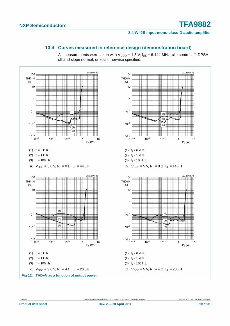
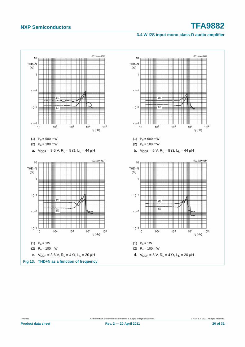
13.4 Curves measured in reference design (demonstration board)All measurements were taken with VDDD = 1.8 V, fclk = 6.144 MHz, clip control off, DPSA off and slope normal, unless otherwise specified.
Product data sheet Rev. 2 — 20 April 2011 24 of 31
NXP Semiconductors TFA98823.4 W I2S input mono class-D audio amplifier
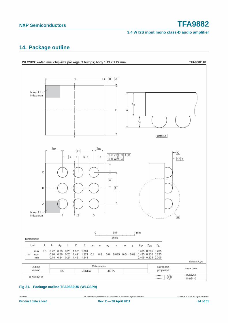
15. Soldering of WLCSP packages
15.1 Introduction to soldering WLCSP packagesThis text provides a very brief insight into a complex technology. A more in-depth account of soldering WLCSP (Wafer Level Chip-Size Packages) can be found in application note AN10439 “Wafer Level Chip Scale Package” and in application note AN10365 “Surface mount reflow soldering description”.
Wave soldering is not suitable for this package.
All NXP WLCSP packages are lead-free.
15.2 Board mountingBoard mounting of a WLCSP requires several steps:
1. Solder paste printing on the PCB2. Component placement with a pick and place machine3. The reflow soldering itself
15.3 Reflow solderingKey characteristics in reflow soldering are:
• Lead-free versus SnPb soldering; note that a lead-free reflow process usually leads to higher minimum peak temperatures (see Figure 22) than a PbSn process, thus reducing the process window
• Solder paste printing issues, such as smearing, release, and adjusting the process window for a mix of large and small components on one board
• Reflow temperature profile; this profile includes preheat, reflow (in which the board is heated to the peak temperature), and cooling down. It is imperative that the peak temperature is high enough for the solder to make reliable solder joints (a solder paste characteristic) while being low enough that the packages and/or boards are not damaged. The peak temperature of the package depends on package thickness and volume and is classified in accordance with Table 17.
Moisture sensitivity precautions, as indicated on the packing, must be respected at all times.
Studies have shown that small packages reach higher temperatures during reflow soldering, see Figure 22.
Table 17. Lead-free process (from J-STD-020C)Package thickness (mm) Package reflow temperature (°C)
Product data sheet Rev. 2 — 20 April 2011 25 of 31
NXP Semiconductors TFA98823.4 W I2S input mono class-D audio amplifier
For further information on temperature profiles, refer to application note AN10365 “Surface mount reflow soldering description”.
15.3.1 Stand offThe stand off between the substrate and the chip is determined by:
• The amount of printed solder on the substrate• The size of the solder land on the substrate• The bump height on the chip
The higher the stand off, the better the stresses are released due to TEC (Thermal Expansion Coefficient) differences between substrate and chip.
15.3.2 Quality of solder jointA flip-chip joint is considered to be a good joint when the entire solder land has been wetted by the solder from the bump. The surface of the joint should be smooth and the shape symmetrical. The soldered joints on a chip should be uniform. Voids in the bumps after reflow can occur during the reflow process in bumps with high ratio of bump diameter to bump height, i.e. low bumps with large diameter. No failures have been found to be related to these voids. Solder joint inspection after reflow can be done with X-ray to monitor defects such as bridging, open circuits and voids.
15.3.3 ReworkIn general, rework is not recommended. By rework we mean the process of removing the chip from the substrate and replacing it with a new chip. If a chip is removed from the substrate, most solder balls of the chip will be damaged. In that case it is recommended not to re-use the chip again.
MSL: Moisture Sensitivity Level
Fig 22. Temperature profiles for large and small components
001aac844
temperature
time
minimum peak temperature= minimum soldering temperature
Product data sheet Rev. 2 — 20 April 2011 26 of 31
NXP Semiconductors TFA98823.4 W I2S input mono class-D audio amplifier
Device removal can be done when the substrate is heated until it is certain that all solder joints are molten. The chip can then be carefully removed from the substrate without damaging the tracks and solder lands on the substrate. Removing the device must be done using plastic tweezers, because metal tweezers can damage the silicon. The surface of the substrate should be carefully cleaned and all solder and flux residues and/or underfill removed. When a new chip is placed on the substrate, use the flux process instead of solder on the solder lands. Apply flux on the bumps at the chip side as well as on the solder pads on the substrate. Place and align the new chip while viewing with a microscope. To reflow the solder, use the solder profile shown in application note AN10365 “Surface mount reflow soldering description”.
15.3.4 CleaningCleaning can be done after reflow soldering.
Product data sheet Rev. 2 — 20 April 2011 28 of 31
NXP Semiconductors TFA98823.4 W I2S input mono class-D audio amplifier
17. Legal information
17.1 Data sheet status
[1] Please consult the most recently issued document before initiating or completing a design.
[2] The term ‘short data sheet’ is explained in section “Definitions”.
[3] The product status of device(s) described in this document may have changed since this document was published and may differ in case of multiple devices. The latest product status information is available on the Internet at URL http://www.nxp.com.
17.2 DefinitionsDraft — The document is a draft version only. The content is still under internal review and subject to formal approval, which may result in modifications or additions. NXP Semiconductors does not give any representations or warranties as to the accuracy or completeness of information included herein and shall have no liability for the consequences of use of such information.
Short data sheet — A short data sheet is an extract from a full data sheet with the same product type number(s) and title. A short data sheet is intended for quick reference only and should not be relied upon to contain detailed and full information. For detailed and full information see the relevant full data sheet, which is available on request via the local NXP Semiconductors sales office. In case of any inconsistency or conflict with the short data sheet, the full data sheet shall prevail.
Product specification — The information and data provided in a Product data sheet shall define the specification of the product as agreed between NXP Semiconductors and its customer, unless NXP Semiconductors and customer have explicitly agreed otherwise in writing. In no event however, shall an agreement be valid in which the NXP Semiconductors product is deemed to offer functions and qualities beyond those described in the Product data sheet.
17.3 DisclaimersLimited warranty and liability — Information in this document is believed to be accurate and reliable. However, NXP Semiconductors does not give any representations or warranties, expressed or implied, as to the accuracy or completeness of such information and shall have no liability for the consequences of use of such information.
In no event shall NXP Semiconductors be liable for any indirect, incidental, punitive, special or consequential damages (including - without limitation - lost profits, lost savings, business interruption, costs related to the removal or replacement of any products or rework charges) whether or not such damages are based on tort (including negligence), warranty, breach of contract or any other legal theory.
Notwithstanding any damages that customer might incur for any reason whatsoever, NXP Semiconductors’ aggregate and cumulative liability towards customer for the products described herein shall be limited in accordance with the Terms and conditions of commercial sale of NXP Semiconductors.
Right to make changes — NXP Semiconductors reserves the right to make changes to information published in this document, including without limitation specifications and product descriptions, at any time and without notice. This document supersedes and replaces all information supplied prior to the publication hereof.
Suitability for use — NXP Semiconductors products are not designed, authorized or warranted to be suitable for use in life support, life-critical or safety-critical systems or equipment, nor in applications where failure or
malfunction of an NXP Semiconductors product can reasonably be expected to result in personal injury, death or severe property or environmental damage. NXP Semiconductors accepts no liability for inclusion and/or use of NXP Semiconductors products in such equipment or applications and therefore such inclusion and/or use is at the customer’s own risk.
Applications — Applications that are described herein for any of these products are for illustrative purposes only. NXP Semiconductors makes no representation or warranty that such applications will be suitable for the specified use without further testing or modification.
Customers are responsible for the design and operation of their applications and products using NXP Semiconductors products, and NXP Semiconductors accepts no liability for any assistance with applications or customer product design. It is customer’s sole responsibility to determine whether the NXP Semiconductors product is suitable and fit for the customer’s applications and products planned, as well as for the planned application and use of customer’s third party customer(s). Customers should provide appropriate design and operating safeguards to minimize the risks associated with their applications and products.
NXP Semiconductors does not accept any liability related to any default, damage, costs or problem which is based on any weakness or default in the customer’s applications or products, or the application or use by customer’s third party customer(s). Customer is responsible for doing all necessary testing for the customer’s applications and products using NXP Semiconductors products in order to avoid a default of the applications and the products or of the application or use by customer’s third party customer(s). NXP does not accept any liability in this respect.
Limiting values — Stress above one or more limiting values (as defined in the Absolute Maximum Ratings System of IEC 60134) will cause permanent damage to the device. Limiting values are stress ratings only and (proper) operation of the device at these or any other conditions above those given in the Recommended operating conditions section (if present) or the Characteristics sections of this document is not warranted. Constant or repeated exposure to limiting values will permanently and irreversibly affect the quality and reliability of the device.
Terms and conditions of commercial sale — NXP Semiconductors products are sold subject to the general terms and conditions of commercial sale, as published at http://www.nxp.com/profile/terms, unless otherwise agreed in a valid written individual agreement. In case an individual agreement is concluded only the terms and conditions of the respective agreement shall apply. NXP Semiconductors hereby expressly objects to applying the customer’s general terms and conditions with regard to the purchase of NXP Semiconductors products by customer.
No offer to sell or license — Nothing in this document may be interpreted or construed as an offer to sell products that is open for acceptance or the grant, conveyance or implication of any license under any copyrights, patents or other industrial or intellectual property rights.
Export control — This document as well as the item(s) described herein may be subject to export control regulations. Export might require a prior authorization from national authorities.
NXP Semiconductors TFA98823.4 W I2S input mono class-D audio amplifier
Quick reference data — The Quick reference data is an extract of the product data given in the Limiting values and Characteristics sections of this document, and as such is not complete, exhaustive or legally binding.
Non-automotive qualified products — Unless this data sheet expressly states that this specific NXP Semiconductors product is automotive qualified, the product is not suitable for automotive use. It is neither qualified nor tested in accordance with automotive testing or application requirements. NXP Semiconductors accepts no liability for inclusion and/or use of non-automotive qualified products in automotive equipment or applications.
In the event that customer uses the product for design-in and use in automotive applications to automotive specifications and standards, customer (a) shall use the product without NXP Semiconductors’ warranty of the
product for such automotive applications, use and specifications, and (b) whenever customer uses the product for automotive applications beyond NXP Semiconductors’ specifications such use shall be solely at customer’s own risk, and (c) customer fully indemnifies NXP Semiconductors for any liability, damages or failed product claims resulting from customer design and use of the product for automotive applications beyond NXP Semiconductors’ standard warranty and NXP Semiconductors’ product specifications.
17.4 TrademarksNotice: All referenced brands, product names, service names and trademarks are the property of their respective owners.
18. Contact information
For more information, please visit: http://www.nxp.com
For sales office addresses, please send an email to: [email protected]