The ALMA Correlator Gianni Comoretto, J.C. Webber, A. Baudry, C.M. Broadwell, R. P. Escoffier, J.H. Greenberg, R.R. Treacy, P. Cais, B Quertier, P. Camino, A. Bos, W Gunst, Workshop on New Generation Correlators Groningen, 27th-29th June, 2006
Transcript
The ALMA Correlator
Gianni Comoretto, J.C. Webber, A. Baudry, C.M. Broadwell,
R. P. Escoffier, J.H. Greenberg, R.R. Treacy, P. Cais, B Quertier,
P. Camino, A. Bos, W Gunst,
Workshop on New Generation Correlators
Groningen, 27th-29th June, 2006
Contents
• The ALMA interferometer
• The correlator
• Time and frequency division modes
• Characteristics and operating modes
• First test results
• Summary
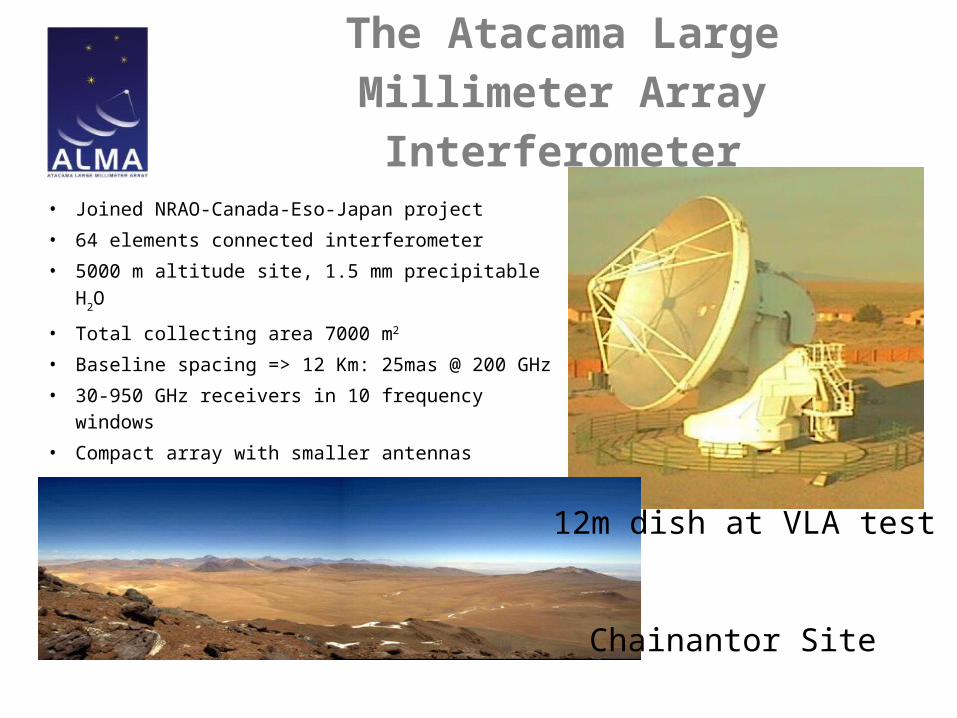
The Atacama Large Millimeter Array
Interferometer
• Joined NRAO-Canada-Eso-Japan project
• 64 elements connected interferometer
• 5000 m altitude site, 1.5 mm precipitable H2O
• Total collecting area 7000 m2
• Baseline spacing => 12 Km: 25mas @ 200 GHz
• 30-950 GHz receivers in 10 frequency windows
• Compact array with smaller antennas
12m dish at VLA test site
Chainantor Site
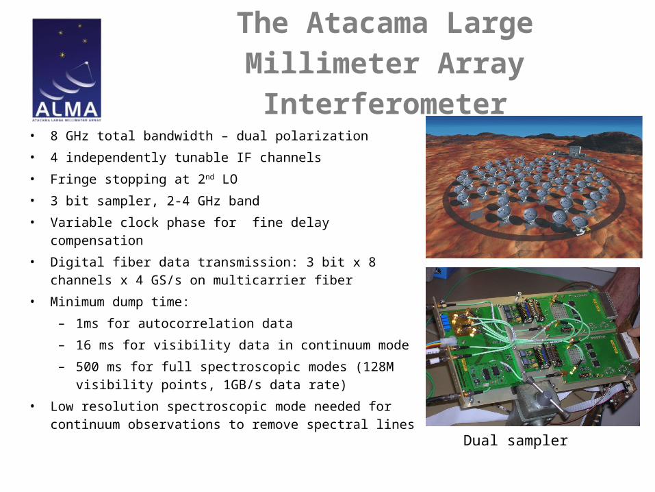
The Atacama Large Millimeter Array
Interferometer
• 8 GHz total bandwidth – dual polarization
• 4 independently tunable IF channels
• Fringe stopping at 2nd LO
• 3 bit sampler, 2-4 GHz band
• Variable clock phase for fine delay compensation
• Digital fiber data transmission: 3 bit x 8 channels x 4 GS/s on
multicarrier fiber
• Minimum dump time:
– 1ms for autocorrelation data
– 16 ms for visibility data in continuum mode
– 500 ms for full spectroscopic modes (128M visibility
points, 1GB/s data rate)
• Low resolution spectroscopic mode needed for continuum
observations to remove spectral lines Dual sampler
The ALMA correlator
• 4 quadrants, each one processing single 2 GHz IF channel
• 4 polarization products, 64 antennas
• Correlator chip: 4K lags at 125 MHz clock, 2 bit sampling
• 4 cards process 1/32 of the IF bandwidth: 512 cards total
• Time division and frequency division modesOne quadrant
Station rack Correlator rackpowersupply
Computer
System design evolution
• Initial design: pure lag correlator, with band selecting digital filter
– Time division architecture: each correlator plane analyzes a time segment
of the input data
– Limited frequency resolution at full BW: 64 points/IF (31 MHz)
– Full resolution (2K points) at 1/32 BW
• Retrofitted with digital filterboard, to implement a frequency division FXF
architecture
– Filterbank performs 32 point frequency division
– Each correlator plane analyzes one frequency segment
– Resolution increases by up to 32 (1 MHz at full BW)
– Filterboard mechanically, electrically and cost compatible with old digital
filter
• Full BW time division mode mantained for “continuum” observations
Correlator structure
• Antenna based design
• Antenna unit: delay compensation, filtering,
recirculating memory
• Correlator unit: 64x64x4 correlators, Long
Term Accumulator
• Minimum number of inteconnections:
– Each antenna unit sends 2 pol. data to 32
correlator units
– Each correlator unit receives data from 64
antenna units
– Point-to-point interconnections, without
data duplication
– LVDS interconnections with 250 MS/s
data rate
Correlator structureAlma Correlator block Diagram
The ALMA correlator chip
• Full custom ASIC at 125 MHz clock
• Conventional lag type real correlator
• 2 bit full multiplication table. 4 blocks can be joined for 4 bit operation
• Individual block: 2 polarization per antenna
– 4x64 lags at full polarization (HH, HV, VH, VV)
– 2x128 lags at dual polarization (HH, VV)
– 256 lags with one polarization
• No cascading of blocks. Larger delays implemented using station based
buffer memory
• 20 bit integration and 16 bit secondary storage
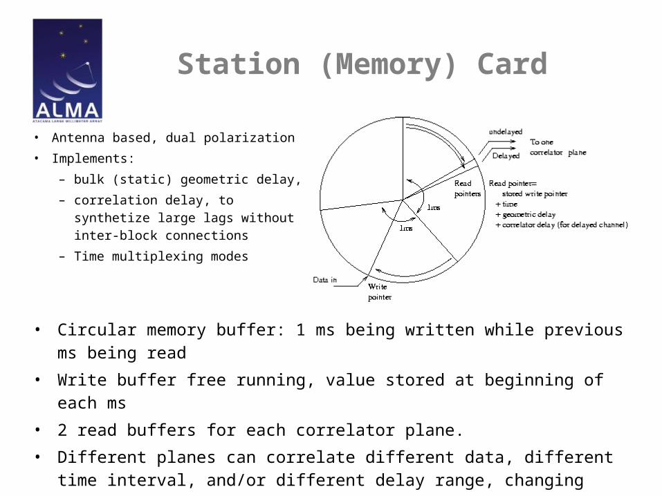
Station (Memory) Card
• Antenna based, dual polarization
• Implements:
– bulk (static) geometric delay,
– correlation delay, to synthetize
large lags without inter-block
connections
– Time multiplexing modes
• Circular memory buffer: 1 ms being written while previous ms being read
• Write buffer free running, value stored at beginning of each ms
• 2 read buffers for each correlator plane.
• Different planes can correlate different data, different time interval, and/or different
delay range, changing only read pointer offset
Time division mode
• 1 ms data block divided into (up to) 32 shorter blocks
• Each block sent at 125 MS/s to one correlator plane
• At 2 GHz BW, 32 correlator planes needed: 64 spectral points total (4 pol. mode)
• At reduced BW, more planes available: each plane processed data with different
delay offset => more lags
• No interconnections between planes, all “routing” performed in memory board
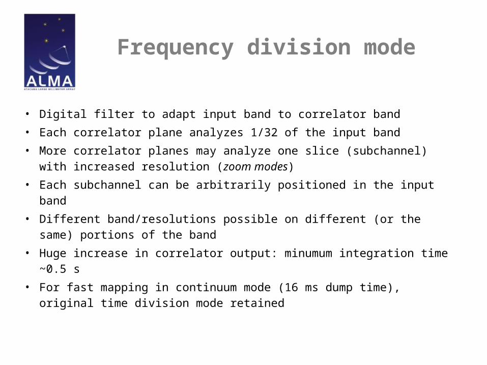
Frequency division mode
• Digital filter to adapt input band to correlator band
• Each correlator plane analyzes 1/32 of the input band
• More correlator planes may analyze one slice (subchannel) with increased
resolution (zoom modes)
• Each subchannel can be arbitrarily positioned in the input band
• Different band/resolutions possible on different (or the same) portions of
the band
• Huge increase in correlator output: minumum integration time ~0.5 s
• For fast mapping in continuum mode (16 ms dump time), original time
division mode retained
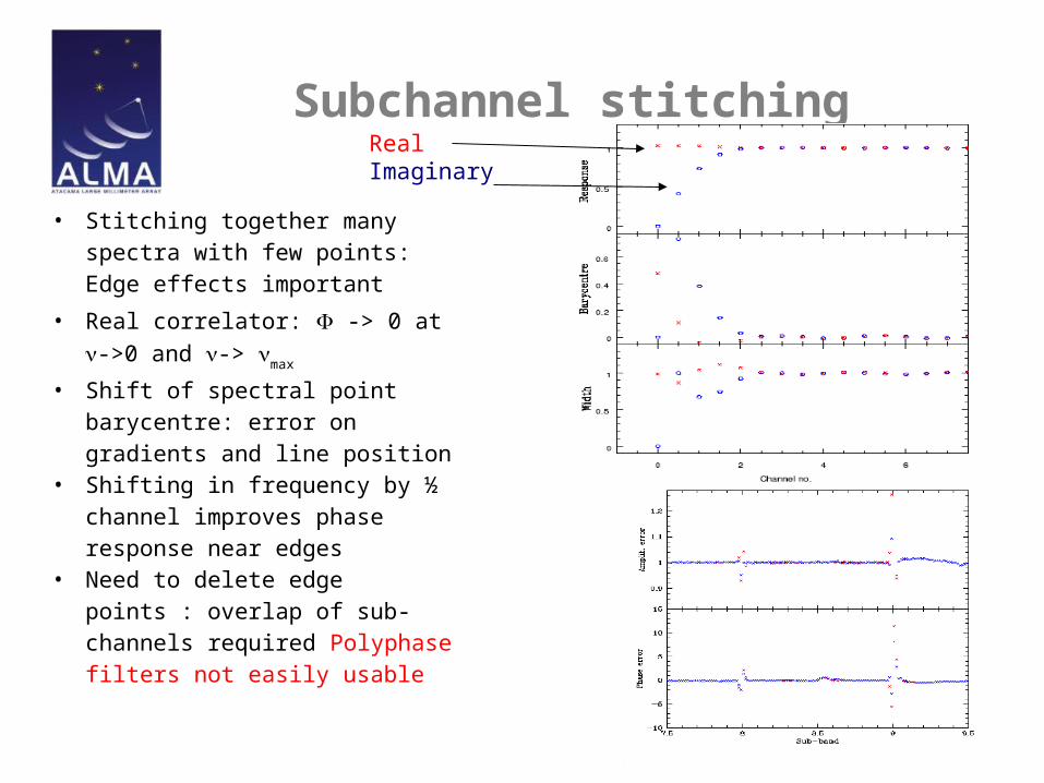
Subchannel stitching
• Stitching together many spectra
with few points: Edge effects
important
• Real correlator: -> 0 at ->0 and
-> max
• Shift of spectral point barycentre:
error on gradients and line position• Shifting in frequency by ½ channel
improves phase response near
edges• Need to delete edge points :
overlap of sub-channels required
Polyphase filters not easily usable
RealImaginary
Tunable Filter Bank
• Array of digital receivers
• Each receiver selects and
downconverts a 62.5 MHz frequency
slot in the input 2 GHz band
• Delay compensation for short term
geometric delay variations
• Implemented using 16 FPGAs
(Altera Stratix2 EP2S30)
• Prone to single-event upset in
configuration RAM: internal CRC
monitor to detect configuration faults
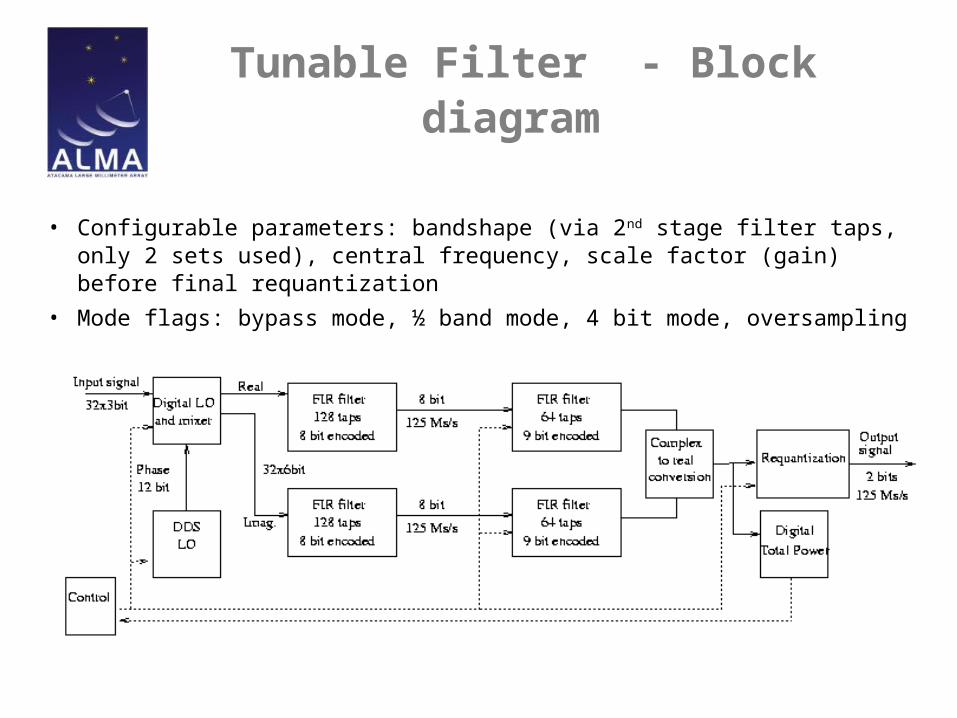
Tunable Filter - Block diagram
• Configurable parameters: bandshape (via 2nd stage filter taps, only 2 sets used), central frequency, scale factor (gain) before final requantization
• Mode flags: bypass mode, ½ band mode, 4 bit mode, oversampling
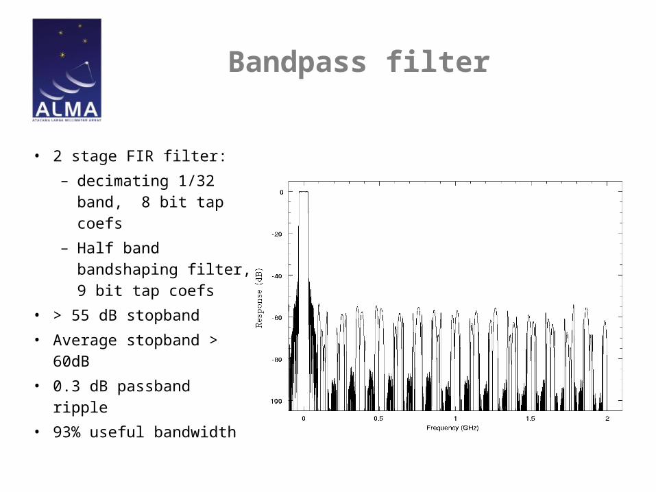
Bandpass filter
• 2 stage FIR filter:
– decimating 1/32 band,
8 bit tap coefs
– Half band
bandshaping filter, 9
bit tap coefs
• > 55 dB stopband
• Average stopband > 60dB
• 0.3 dB passband ripple
• 93% useful bandwidth
Dynamic range and noise
• Dynamic range
– Polyphase digital LO/mixer using 6 bit
lookup tables: 0.9% loss, > 52 dB SFDR
– Filter: 55 dB stopband rejection
• Excess noise:
– 3 bit + 2 bit quantizations increase quant.
noise
– Possibility of trading BW for sensitivity
Sampler Mixer Total
Bypass 2 bit 13.6 13.6
Bypass 3 bit 4.1 4.1
Freq. division:
2 bit 4.1 0.1 13.6 18.3
4.1 0.1 ~8.0 ~12.0
2nd Quant
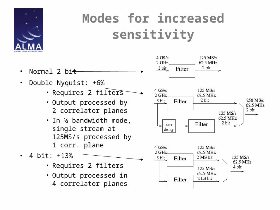
Modes for increased sensitivity
• Normal 2 bit
• Double Nyquist: +6%
• Requires 2 filters
• Output processed by 2 correlator planes
• In ½ bandwidth mode, single stream at 125MS/s processed by 1 corr. plane
• 4 bit: +13%
• Requires 2 filters
• Output processed in 4 correlator planes
Implementation
• Signal distribution direct point-to-point
LVCMOS
• Connections only between adjacent
chips
• Interboard connections point-to-point
PECL
• Signal integrity checkers on each data
path. Programmable signal phase
• Clock distribution using internal FPGA
PLL.
• Inter-rack connections 250 MHz LVDS
cables
• Power distribution using onboard DC-
DC converter, 48V busDigital filterboard
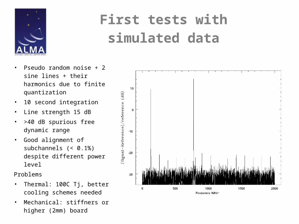
First tests with simulated data
• Pseudo random noise + 2 sine
lines + their harmonics due to
finite quantization
• 10 second integration
• Line strength 15 dB
• >40 dB spurious free dynamic
range
• Good alignment of subchannels
(< 0.1%) despite different power
level
Problems
• Thermal: 100C Tj, better cooling
schemes needed
• Mechanical: stiffners or higher
(2mm) board
Summary
• Connected element interferometer, using digital fiber link interconnection• Spectral line output, full polarization (4 pol channels)• Total BW 8+8 GHz, digitized as 4+4 channels 2 GHz, 3 bit• Resolution channels mode over 2 GHz IF (single quadrant):
– 31 MHz 64 fast continuum mode, full polarization – 1 MHz 2048 Frequency division mode, full band & polarization– 250 KHz 8192 Full band, single polarization– 3.8 KHz 8192 minimum band (31 MHz/IF), single polarization
• 64 antennas: 64 ACF, 2K CCF, with up to 1K frequency and polarization channels per baseline,
total of up to 128M lags • Dump time, limited by total data rate (1 GB/s): 16 ms / 500 ms. Typ. up to minutes• Dynamic range: ~50 dB• Technology: full custom ASIC for correlator, FPGA for filterbank • Correlator board size limits n. of antennas. All ACF and CCF on one board group. Scalable in
bandwidth and resolution, adding “planes”• FXF with first F stage performed using tunable filterbank