832 IEEETRANSACTIONSON MICROWAVETHEORYAND TECHNIQUES, VOL. MTT-30, NO. 5, MAY 1982 isolator at all. Examination of Figs. 3(b), (c), and (d) reveals that a TE,0 signal incident from the right at port 2 exits port 1 in the TEO1 -mode, is reflected, exits port 2 in the same mode, is again reflected, and ultimately exits port 1 unimpeded in the TE lo-mode. III. DISCUSSION Our motivation for examining the inherent noise of isolators came from the fact that we wished to use them in a noise measurement system at 94 GHz, with the goal of detecting the quantum noise of devices at 2 K. Some details of the measure- ment system envisioned are given in a companion paper [2]. It became obvious that the Nyquist noise due to the termination of port 3 of a circulator used as an isolator would be intolerable for our purpose. Naively, we thought that a Faraday rotation isolator embodied in the form of Fig. 2 might behave differently. We then undertook the analysis given above and discovered, much to our surprise, that it behaved exactly as a terminated circulator. Only then did we discover Siegman’s incontrovertible and beautifully simple proof of that fact. IV. CONCLUSION To achieve isolation between its input and output ports, an isolator must include at least one resistive source of Nyquist noise. That noise emanates from its input port. Siegman’s ther- modynamic proof cannot be denied. ACKNOWLEDGMENT This work was supported by National Science Foundation Grant ECS-8007623. A. van der Ziel sumested to the author that the [1] [~] .. inherent noise of an isolator required exploration. l@FERENCES A E S1egman, “Thermal noise m mrcrowave systems, part I,” Mzcro- uaoe J., VOI 4. pp. 81–90, Mar 1961. A. D. Sutherland and A. van der Ziel, “Some pitfalls in rndhmeter-wave noise measurements utdrr.ing a cross-correlation recemer,” IEEE Trans. A4wrowaoe Theoty Tech., this issue, 715-718. The Exact Noise Figure of Amplifiers with Parallel Feedback and Lossy Matching Circuits KARL B, NICLAS, SENIOR MEMBER, IEEE .4stracf —Exact formulas for the noise parameters and noise figure of amplifiers with parallel feedback and Iossy input and output matching circuits are derived. The formulas wkich take into account the thermal agitation of all circuit elements are applicable to feedback and Iossy match amplifiers, as well as amplifiers that employ both principles simultaneously. I. INTRODUCTION Recent developments in the design of single-ended GRAS MESFET amplifiers have focused on two principles, parallel feedback and lossy matching [1 ]–[3]. Either principle has enor- mous bandwidth potential, ranging from a few megahertz all the way into Ku-band. Investigation of the noise in microwave Manuscnpt recewed October 12, 1981; revised December 15, 1981. The author M with the Devices Group, Watkins-Johnson Company, 3333 Hdlview Ave , Stanford Industrml Park, Palo Alto, CA 94304. amplifiers with parallel feedback have proven their feasibility y for low-noise amplification [4]. When comparing noise figures of feedback amplifiers with those of equivalent amplifiers that use Iossy matching circuits, the latter exhibit both, higher theoretical and measured values [5]. However, the lossy match amplifier has the advantage that de-biasing can be accomplished without ser- iously reducing the amplifier’s bandwidth potential in the mega- hertz region. A compromise in electncaf performance may be found in the combination of both principles. Employing parallel feedback and/or lossy matching for low- noise applications requires a qualitative study of the influence of all circuit components on the amplifier’s noise figure. Several papers on the noise figure of amplifiers with parallel feedback have been published over the last eight years [6]–[9]. Howeverj except for [9] the published results do not take into account the inherent noise sources of the transforming two-ports and there- fore cannot be applied to amplifiers that make use of resistive feedback and/or lossy matching networks. This paper develops the exact formulas for the equivalent noise parameters and the noise figure of an amplifier that simultaneously uses parallel feedback and lossy matching while allowing for the thermaf noise agitation of all circuit elements. Due to the fact that the results presented here differ from those obtained by applying the for- mulas presented in [9], a step-by-step account of the derivations is given in the Appendix. II. NOISE FIGURE AND EQUIVALENT NOISE PARAMETERS To study the noise of a two-port with internal noise sources, it is replaced by a noise-free two-port preceded by a simple circuit containing its equivalent noise parameters [1 O]. The latter consists of the equivalent noise resistance R., the equivalent noise con- ductance G., and the correlation admittance & = GCO,+ jBCOr. The parameters R., G., and YCO,can be calculated in case the noise figure for optimum noise matching F~,n, the corresponding signal source admittance Y,mn = G,~,. + Jll,m., and one other noise figure F and its corresponding signal source admittance ~ = G, + jl?,, preferably Y,= Z;’, are known. The noise figure of a two-port can be expressed by the well- known formulas [10], [11] F=Fro,. +:( Gs-G,m,n)2+~(~s -~stin)2 (1) s s with F~,n= 1+2[RtiGCOr+~~] (2) The circuit whose overall noise figure we want to determine is shown in Fig. 1(a). It consists of a noisy two-port at temperature T embedded in a n-shaped network of three admittances Y~, YF~, and Y~. They contain the conductance G~, GFB, and G~ which inject noise into the overall two-port of Fig. 1(a) and thereby contribute to the noise figure of the overall network. In Fig. l(b) all intemaf noise sources of the embedded two-port and the surrounding admittances have been extracted and are represented as external noise voltages (o,, OFB ) and noise cur- rents (i,, z~, z~). This step puts all circuit elements and the embedded two-port at T= O K. The network of Fig. 1(b) will now be used to determine the noise parameters as shown in Fig. 1(c). In doing so, we follow the procedure as outlined in [4] based on [10]. The admittance matrix of the noiseless network of Fig. 1(c) representing the signal voltages and currents takes the form 0018-9480/82 /0500-0832 $00.75 ~1982 IEEE
Transcript
832 IEEETRANSACTIONSON MICROWAVETHEORYAND TECHNIQUES, VOL. MTT-30, NO. 5, MAY 1982
isolator at all. Examination of Figs. 3(b), (c), and (d) reveals that
a TE,0 signal incident from the right at port 2 exits port 1 in the
TEO1 -mode, is reflected, exits port 2 in the same mode, is again
reflected, and ultimately exits port 1 unimpeded in the TE lo-mode.
III. DISCUSSION
Our motivation for examining the inherent noise of isolators
came from the fact that we wished to use them in a noise
measurement system at 94 GHz, with the goal of detecting the
quantum noise of devices at 2 K. Some details of the measure-
ment system envisioned are given in a companion paper [2]. It
became obvious that the Nyquist noise due to the termination of
port 3 of a circulator used as an isolator would be intolerable for
our purpose. Naively, we thought that a Faraday rotation isolator
embodied in the form of Fig. 2 might behave differently. We then
undertook the analysis given above and discovered, much to our
surprise, that it behaved exactly as a terminated circulator. Only
then did we discover Siegman’s incontrovertible and beautifully
simple proof of that fact.
IV. CONCLUSION
To achieve isolation between its input and output ports, an
isolator must include at least one resistive source of Nyquist
noise. That noise emanates from its input port. Siegman’s ther-
modynamic proof cannot be denied.
ACKNOWLEDGMENT
This work was supported by National Science Foundation
Grant ECS-8007623. A. van der Ziel sumested to the author that
the
[1]
[~]
. .inherent noise of an isolator required exploration.
l@FERENCES
A E S1egman, “Thermal noise m mrcrowave systems, part I,” Mzcro-
uaoe J., VOI 4. pp. 81–90, Mar 1961.
A. D. Sutherland and A. van der Ziel, “Some pitfalls in rndhmeter-wave
noise measurements utdrr.ing a cross-correlation recemer,” IEEE Trans.
A4wrowaoe Theoty Tech., this issue, 715-718.
The Exact Noise Figure of Amplifiers with Parallel
Feedback and Lossy Matching Circuits
KARL B, NICLAS, SENIOR MEMBER, IEEE
.4stracf —Exact formulas for the noise parameters and noise figure of
amplifiers with parallel feedback and Iossy input and output matching
circuits are derived. The formulas wkich take into account the thermal
agitation of all circuit elements are applicable to feedback and Iossy match
amplifiers, as well as amplifiers that employ both principles simultaneously.
I. INTRODUCTION
Recent developments in the design of single-ended GRAS
MESFET amplifiers have focused on two principles, parallel
feedback and lossy matching [1 ]–[3]. Either principle has enor-
mous bandwidth potential, ranging from a few megahertz all the
way into Ku-band. Investigation of the noise in microwave
Manuscnpt recewed October 12, 1981; revised December 15, 1981.
The author M with the Devices Group, Watkins-Johnson Company, 3333
Hdlview Ave , Stanford Industrml Park, Palo Alto, CA 94304.
amplifiers with parallel feedback have proven their feasibility y for
low-noise amplification [4]. When comparing noise figures of
feedback amplifiers with those of equivalent amplifiers that use
Iossy matching circuits, the latter exhibit both, higher theoretical
and measured values [5]. However, the lossy match amplifier has
the advantage that de-biasing can be accomplished without ser-
iously reducing the amplifier’s bandwidth potential in the mega-
hertz region. A compromise in electncaf performance may be
found in the combination of both principles.
Employing parallel feedback and/or lossy matching for low-
noise applications requires a qualitative study of the influence of
all circuit components on the amplifier’s noise figure. Several
papers on the noise figure of amplifiers with parallel feedback
have been published over the last eight years [6]–[9]. Howeverj
except for [9] the published results do not take into account the
inherent noise sources of the transforming two-ports and there-
fore cannot be applied to amplifiers that make use of resistive
feedback and/or lossy matching networks. This paper develops
the exact formulas for the equivalent noise parameters and the
noise figure of an amplifier that simultaneously uses parallel
feedback and lossy matching while allowing for the thermaf noise
agitation of all circuit elements. Due to the fact that the results
presented here differ from those obtained by applying the for-
mulas presented in [9], a step-by-step account of the derivations
is given in the Appendix.
II. NOISE FIGURE AND EQUIVALENT NOISE PARAMETERS
To study the noise of a two-port with internal noise sources, it
is replaced by a noise-free two-port preceded by a simple circuit
containing its equivalent noise parameters [1 O]. The latter consists
of the equivalent noise resistance R., the equivalent noise con-
ductance G., and the correlation admittance & = GCO,+ jBCOr.
The parameters R., G., and YCO,can be calculated in case the
noise figure for optimum noise matching F~,n, the corresponding
signal source admittance Y,mn = G,~,. + Jll,m., and one other
noise figure F and its corresponding signal source admittance
~ = G, + jl?,, preferably Y,= Z;’, are known.
The noise figure of a two-port can be expressed by the well-
known formulas [10], [11]
F=Fro,.+:( Gs-G,m,n)2+~(~s-~stin)2 (1)s s
with
F~,n= 1+2[RtiGCOr+~~] (2)
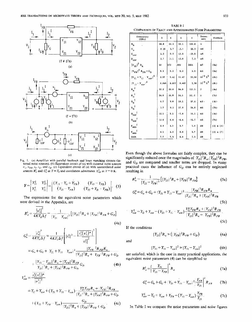
The circuit whose overall noise figure we want to determine is
shown in Fig. 1(a). It consists of a noisy two-port at temperature
T embedded in a n-shaped network of three admittances Y~, YF~,
and Y~. They contain the conductance G~, GFB, and G~ which
inject noise into the overall two-port of Fig. 1(a) and thereby
contribute to the noise figure of the overall network.
In Fig. l(b) all intemaf noise sources of the embedded two-port
and the surrounding admittances have been extracted and are
represented as external noise voltages (o,, OFB ) and noise cur-
rents (i,, z~, z~). This step puts all circuit elements and the
embedded two-port at T= O K.
The network of Fig. 1(b) will now be used to determine the
noise parameters as shown in Fig. 1(c). In doing so, we follow the
procedure as outlined in [4] based on [10]. The admittance matrix
of the noiseless network of Fig. 1(c) representing the signal
voltages and currents takes the form
0018-9480/82 /0500-0832 $00.75 ~1982 IEEE
IEEETRANSACTIONSON MICROWAVETHEORYAND TECHNIQUES, VOL. MTT-30, NO. 5, MAY 1982 833
— 1— —_
II I
“diiil!av’I
(T+ O°K)
(a)
‘FE
(b)
“&‘2
m
I I’11 ’12
I I‘2
’21 ’22
(c)
Fig. 1. (a) Amplifier with parallel feedback and lossy matching circmts (in-
ternal noise sources), (b) Equivalent circuit of (a) with external noise sources
o,, OFB, t,, LG. and ~~. (c) Equivalent circuit of (a) with uncorrelated noise
sources R\ and G; at T = TO and correlation admittance YC~r at T’= O K.