40
Enabling a Microelectronic World ® R. Huemoeller SVP, Adv. Product / Platform Develop June 2013 The Future of Packaging ~ Advanced System Integration
| Date post: | 04-Jun-2018 |
| Category: |
Documents |
| Upload: | dinhkhuong |
| View: | 222 times |
| Download: | 1 times |

Enabling a
Microelectronic
World®
R. Huemoeller
SVP, Adv. Product / Platform Develop
June 2013
The Future of Packaging
~ Advanced System Integration
Jun-13, R.Huemoeller 2 Amkor Info for Controlled Release at Russia Semi
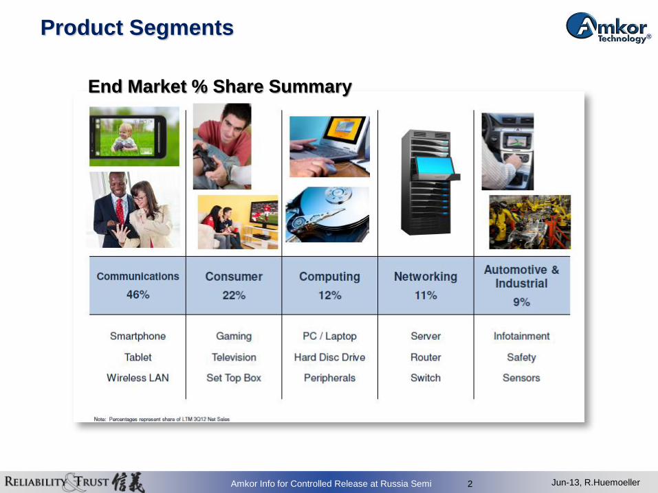
Product Segments
End Market % Share Summary
Jun-13, R.Huemoeller 3 Amkor Info for Controlled Release at Russia Semi
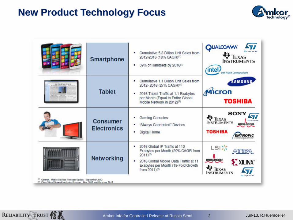
New Product Technology Focus

Jun-13, R.Huemoeller 4 Amkor Info for Controlled Release at Russia Semi
Market Direction & Drivers

Jun-13, R.Huemoeller 5 Amkor Info for Controlled Release at Russia Semi
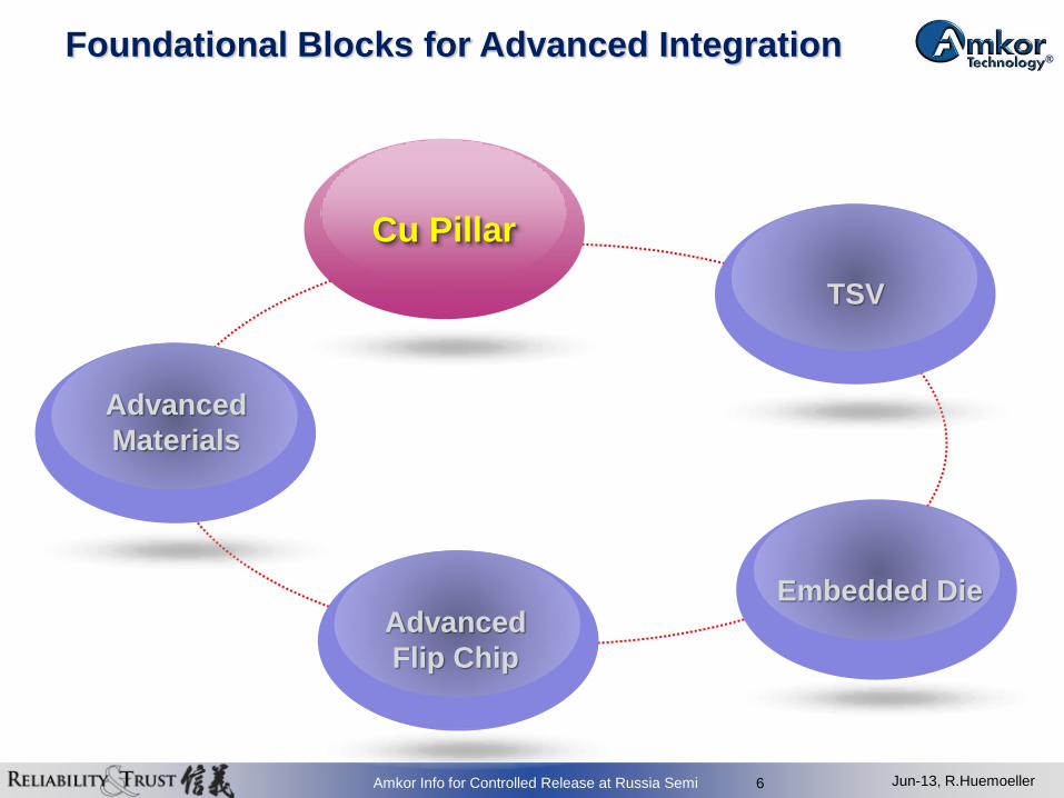
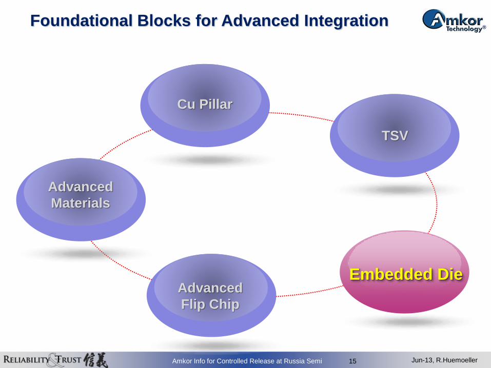
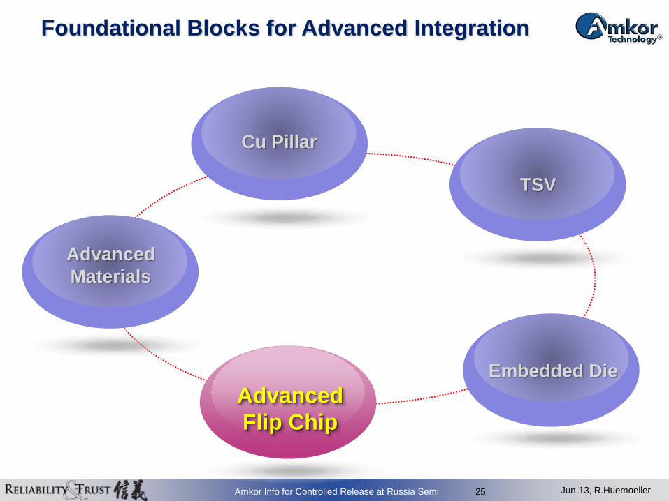
Foundational Blocks for Advanced Integration
Embedded Die
Advanced
Materials
Cu Pillar
TSV
Advanced
Flip Chip
Jun-13, R.Huemoeller 6 Amkor Info for Controlled Release at Russia Semi
Foundational Blocks for Advanced Integration
Embedded Die
Advanced
Materials
Cu Pillar
TSV
Advanced
Flip Chip
Jun-13, R.Huemoeller 7 Amkor Info for Controlled Release at Russia Semi
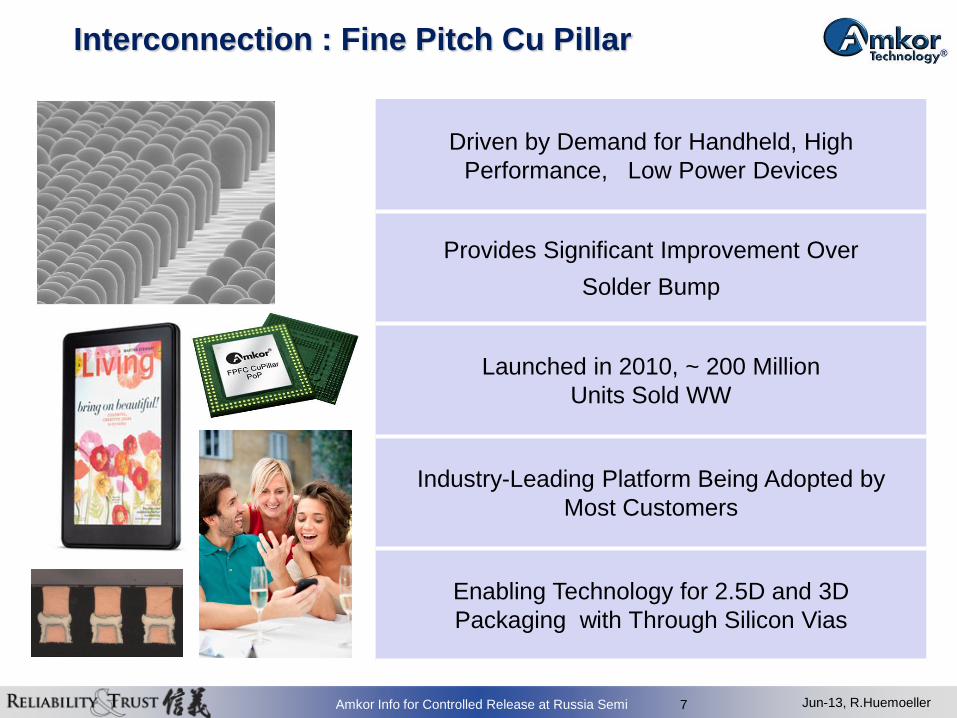
Interconnection : Fine Pitch Cu Pillar
Driven by Demand for Handheld, High
Performance, Low Power Devices
Provides Significant Improvement Over
Solder Bump
Launched in 2010, ~ 200 Million
Units Sold WW
Industry-Leading Platform Being Adopted by
Most Customers
Enabling Technology for 2.5D and 3D
Packaging with Through Silicon Vias

Jun-13, R.Huemoeller 8 Amkor Info for Controlled Release at Russia Semi
Digital Baseband
Applications Processor
Networking ASICs
Digital TV ASICs
Power Management
Embedded Processing – DSP, MCU,
Digital Media
Function Integration in All Three
Dimensions
Silicon Node “Shrinks” But Die
Size Remains Unchanged
Increased I/O Density
Finer BGA Pitch
More Demanding Warpage and
Coplanarity Criteria
Technology Trends Devices
Why the Need for Cu Pillar?

Jun-13, R.Huemoeller 9 Amkor Info for Controlled Release at Russia Semi
Amkor FPFC Technology
• From Standard CSP Package Structure
• To Broad Package Application
PSfcCSP fcCSP
TMV™ PoP FCBGA
Fine Pitch Cu Pillar Formats

Jun-13, R.Huemoeller 10 Amkor Info for Controlled Release at Russia Semi
WLFO
Thermal &
Adv. Materials
Cu Pillar
TSV
High-End FC
Foundational Blocks for Advanced Integration
Jun-13, R.Huemoeller 11 Amkor Info for Controlled Release at Russia Semi
Integration : Through Silicon Via (TSV)
• Current Status
World‟s first production fully integrated TSV package platform completed
“Logic dies on Si interposer” product is being produced
Large number of customers engaged in active TSV development
Future Target devices
Logics on Si interposer
Logics + memories on Si interposer
Memory / Memory stack
Memory / Logic combination
Jun-13, R.Huemoeller 12 Amkor Info for Controlled Release at Russia Semi
2.5D Multi-Chip Interposer Breakdown
• High End Products : Networking, Servers
─ Silicon interposers ; < 2um L/S, < 15nsec latency, > 25k µbumps per die
─ Several foundries delivering silicon interposers today
─ Others in consideration of adding capability to make use of unused assets
• Mid Range Products : Gaming, Graphics, HDTV, Adv. Tablets
─ Silicon or Glass interposers ; < 3um L/S, < 25nsec latency, ~10k µbumps/die
─ Glass may provide cost reduction path in future
─ Glass interposers infrastructure still immature, but improving
• Low Cost Products : Lower End Tablets, Smart Phones
─ Organic interposer?? ; < 8um L/S, low resistance, ~2k µbumps
─ Must provide cost reduction path to enable this sector ; thick copper traces
─ Possible elimination of laminate substrate, but organic interposer as substrate!!
Jun-13, R.Huemoeller 13 Amkor Info for Controlled Release at Russia Semi
Memory
• Sources
─ End customer choosing memory supplier
─ Memory supply chain is constrained today
─ 2 different sources – Elpida (Micron) & Hynix
• Logistics
─ Plan is to receive memory as „KGM‟ on tape and reel
─ End customer will manage logistics through consignment models
• Activity
─ Multiple programs in progress with stacked memory in wide I/O format
HBM or Wide-IO2
– Shipping single die, 2 die stacks and 4 die stacks already
– Most development being completed with 4 die stacks now
Jun-13, R.Huemoeller 14 Amkor Info for Controlled Release at Russia Semi
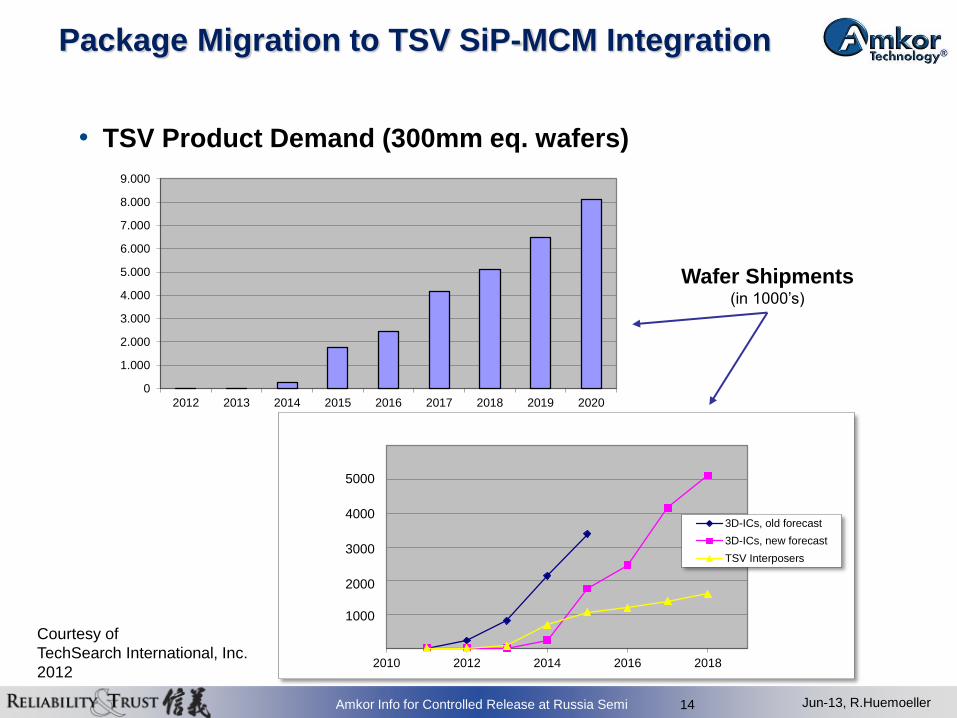
0
1.000
2.000
3.000
4.000
5.000
6.000
7.000
8.000
9.000
2012 2013 2014 2015 2016 2017 2018 2019 2020
2010 2012 2014 2016 2018
3D-ICs, old forecast
3D-ICs, new forecast
TSV Interposers
5000
4000
3000
2000
1000
Package Migration to TSV SiP-MCM Integration
Wafer Shipments (in 1000‟s)
• TSV Product Demand (300mm eq. wafers)
Courtesy of
TechSearch International, Inc.
2012
Jun-13, R.Huemoeller 15 Amkor Info for Controlled Release at Russia Semi
Embedded Die
Advanced
Materials
Cu Pillar
TSV
Advanced
Flip Chip
Foundational Blocks for Advanced Integration

Jun-13, R.Huemoeller 16 Amkor Info for Controlled Release at Russia Semi
Embedded Die : 3 Levels of Architecture
Wafer Level
Die
Substrate Level
Passive Components
Active Die
Single Die
Multi-Die
3D Package
Single Die
Multi-Die
3D Pkg
– Passive integration
– Internal EMI shielding possibilities
– Multi-die capability – more than one die may be embedded
– Two-sided construction – top side components may be mounted
Jun-13, R.Huemoeller 17 Amkor Info for Controlled Release at Russia Semi
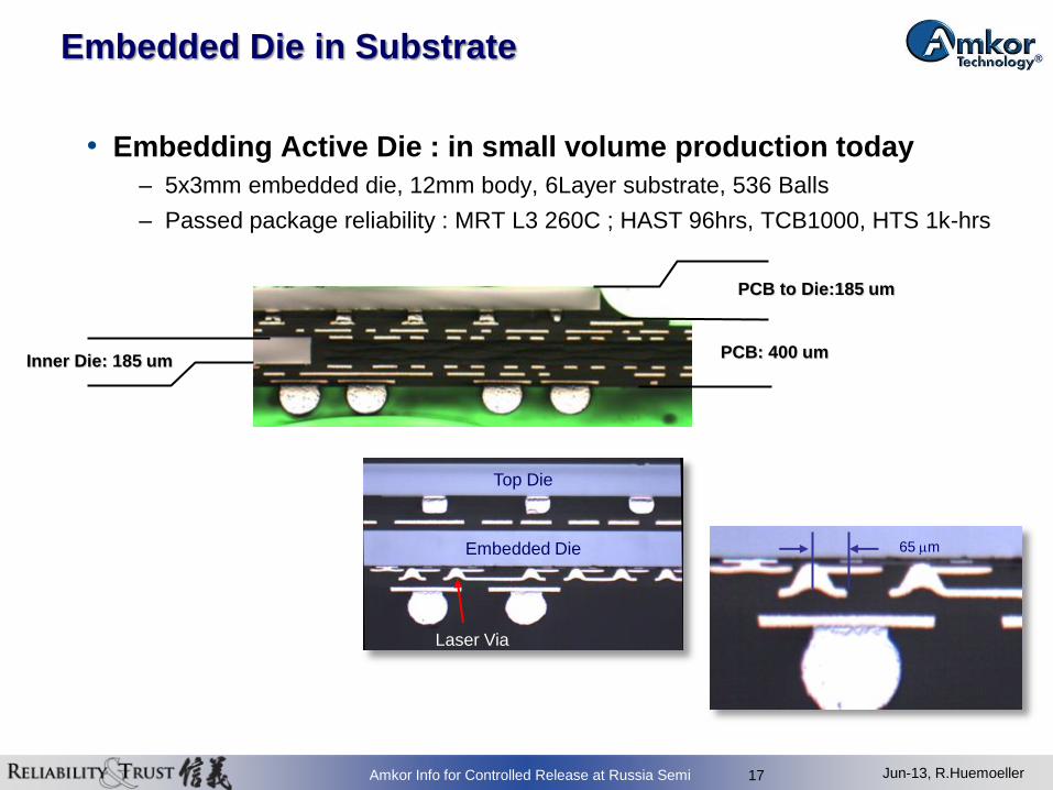
• Embedding Active Die : in small volume production today
– 5x3mm embedded die, 12mm body, 6Layer substrate, 536 Balls
– Passed package reliability : MRT L3 260C ; HAST 96hrs, TCB1000, HTS 1k-hrs
Embedded Die
Top Die
Laser Via
65 mm
Embedded Die in Substrate
PCB: 400 um
PCB to Die:185 um
Inner Die: 185 um
Jun-13, R.Huemoeller 18 Amkor Info for Controlled Release at Russia Semi
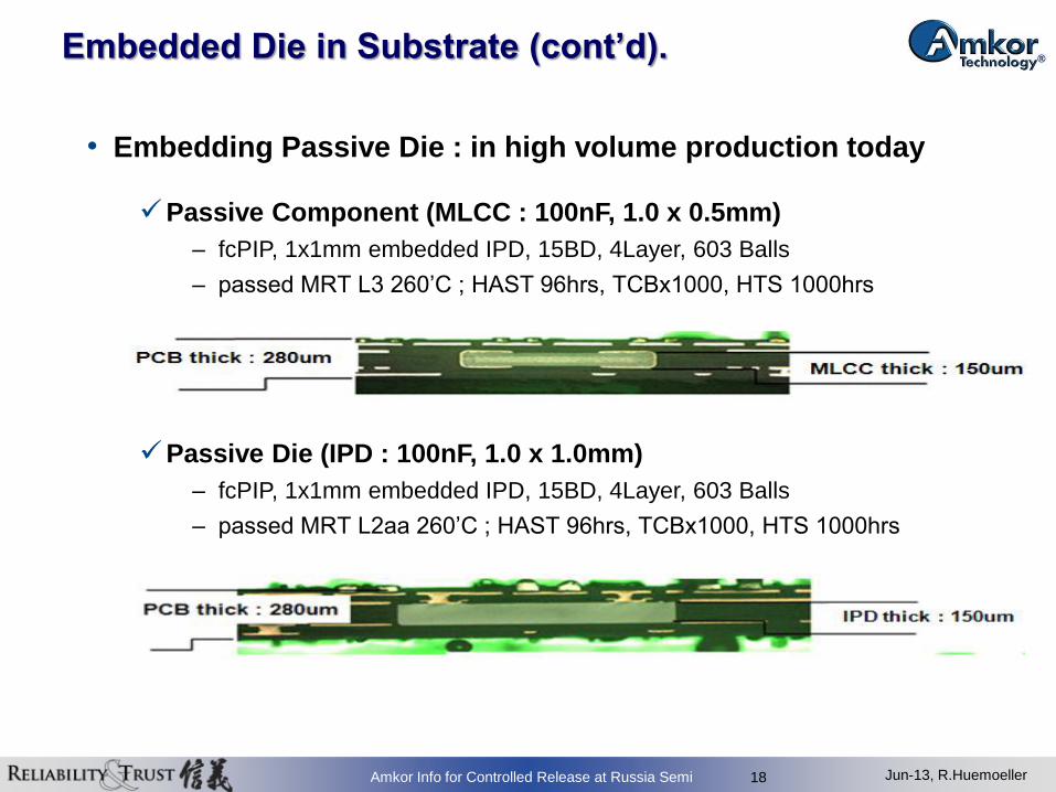
Embedded Die in Substrate (cont’d).
Passive Component (MLCC : 100nF, 1.0 x 0.5mm)
– fcPIP, 1x1mm embedded IPD, 15BD, 4Layer, 603 Balls
– passed MRT L3 260‟C ; HAST 96hrs, TCBx1000, HTS 1000hrs
Passive Die (IPD : 100nF, 1.0 x 1.0mm)
– fcPIP, 1x1mm embedded IPD, 15BD, 4Layer, 603 Balls
– passed MRT L2aa 260‟C ; HAST 96hrs, TCBx1000, HTS 1000hrs
• Embedding Passive Die : in high volume production today

Jun-13, R.Huemoeller 19 Amkor Info for Controlled Release at Russia Semi
• Embedded die on Wafer
– Product capability up to 15x15mm, 0.4mm pitch, 1000 I/O+
– 300mm formats
– Fully deployed for several years now
Advanced Platform : Wafer Based Fan Out

Jun-13, R.Huemoeller 20 Amkor Info for Controlled Release at Russia Semi
Large I/O Count Without Die Increase
3D PKG Platform Creation
Core Technology Development
Entry
Expand
Cost Reduce
Die
Die
Die Shrink Continuing
Face to Face
Customer / Product Base Widens
PoP/Sensor Application
No Wire or Substrate
• Customer Interest
– Hybrid Packages, RF Connectivity, Audio modules & Sensor Applications
Advanced Platform : Wafer Based Fan Out (Cont’d)
niche
growing

Jun-13, R.Huemoeller 21 Amkor Info for Controlled Release at Russia Semi
Market Growth for Wafer Fan Out Packages
• Single die solutions remain niche to market ; primarily one customer driving use

Jun-13, R.Huemoeller 22 Amkor Info for Controlled Release at Russia Semi
Evolution of Wafer Based Fan Out
• Wafer Fan Out 3D Products
– Customer interest expanding to two sided structures
– Requiring more functionality
– Ultimate goal is multi chip in smallest form factor
Die
Die
.
3D-WLFO Benefits
H
Die
Die
Die
Die
Die
Die
3D-WLFO Benefits
Die
Die
Thru
Mold Via

Jun-13, R.Huemoeller 23 Amkor Info for Controlled Release at Russia Semi
Market Growth for Wafer Fan Out Packages
• Multi die solutions will drive future market ; triggers growth phase
Jun-13, R.Huemoeller 24 Amkor Info for Controlled Release at Russia Semi
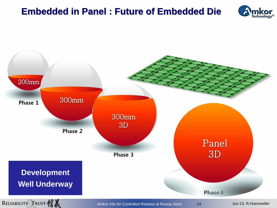
200mm
Phase 1 300mm
Phase 2
Embedded in Panel : Future of Embedded Die
Phase 3
300mm 300mm
3D
Development
Well Underway Phase 4
Panel3D
Jun-13, R.Huemoeller 25 Amkor Info for Controlled Release at Russia Semi
Embedded Die
Advanced
Materials
Cu Pillar
TSV
Advanced
Flip Chip
Foundational Blocks for Advanced Integration
Jun-13, R.Huemoeller 26 Amkor Info for Controlled Release at Russia Semi
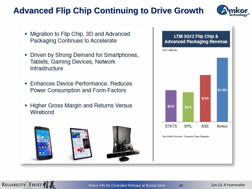
Advanced Flip Chip Continuing to Drive Growth

Jun-13, R.Huemoeller 27 Amkor Info for Controlled Release at Russia Semi
• Industry Direction
Increasing body size (>55mm BD)
Increasing die size (>26mm)
32/28nm in production with 20nm qualification in progress
Cu Pillar to enable density / pitch below 150um bump pitch
Coreless substrates in use for 32/28nm
Multiple die per package …. With die count continuing to increase
High Performance Flip Chip
Jun-13, R.Huemoeller 28 Amkor Info for Controlled Release at Russia Semi
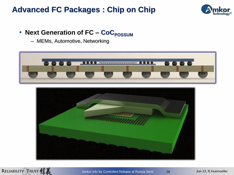
Advanced FC Packages : Chip on Chip
• Next Generation of FC – CoCPOSSUM
– MEMs, Automotive, Networking

Jun-13, R.Huemoeller 29 Amkor Info for Controlled Release at Russia Semi
LOGIC (780um thickness)
ASIC (60um thickness)
40um bump pitch CoC Technology
Heat Spreader
200um bump pitch
LOGIC
Substrate
Cu pillar with LF solder
+ microbump
Advanced FC Packages : Chip on Chip, cont.
• 2014 Targeted production
Networking ASIC + FPGA
Microcontroller ASIC + Memory
Automotive ASIC + Memory

Jun-13, R.Huemoeller 30 Amkor Info for Controlled Release at Russia Semi
Embedded Die
Cu Pillar
TSV
Advanced
Flip Chip
Advanced
Materials
Foundational Blocks for Advanced Integration
Jun-13, R.Huemoeller 31 Amkor Info for Controlled Release at Russia Semi
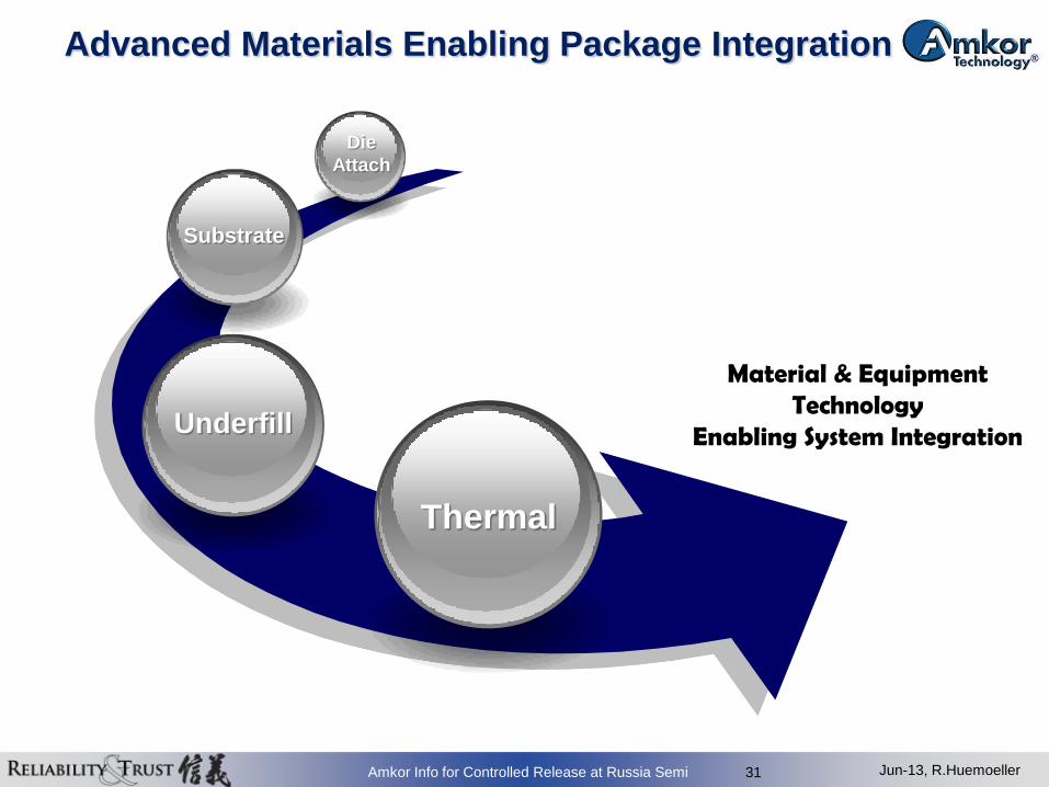
Substrate
Material & Equipment Technology
Enabling System Integration
Advanced Materials Enabling Package Integration
Die
Attach
Underfill
Thermal
Jun-13, R.Huemoeller 32 Amkor Info for Controlled Release at Russia Semi
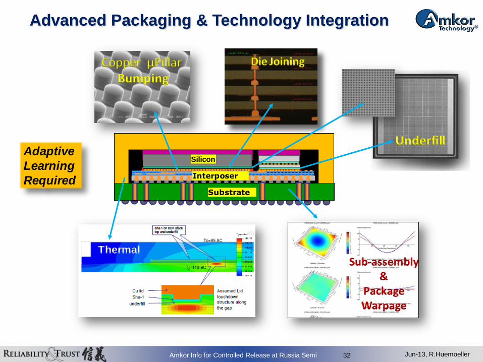
Advanced Packaging & Technology Integration
Copper µPillar Bumping
Underfill
Sub-assembly &
Package Warpage
Thermal
Substrate
Interposer
Silicon
Die Joining
Adaptive
Learning
Required

Jun-13, R.Huemoeller 33 Amkor Info for Controlled Release at Russia Semi
Embedded Die
Advanced
Materials
Cu Pillar
TSV
Advanced
Flip Chip
Foundational Blocks for Advanced Integration

Jun-13, R.Huemoeller 34 Amkor Info for Controlled Release at Russia Semi
Advanced Package Integration Becoming Clearer Sm
aller F
orm
Facto
r Larg
er
Interconnect Density & Functionality : Increasing
Wafer Level
Die
Board Level
LOGIC
ASIC
CoCpossum™
Die Level
Jun-13, R.Huemoeller 35 Amkor Info for Controlled Release at Russia Semi
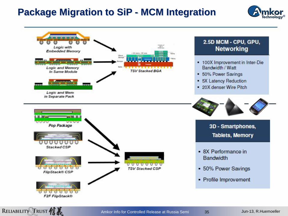
Package Migration to SiP - MCM Integration
Jun-13, R.Huemoeller 36 Amkor Info for Controlled Release at Russia Semi
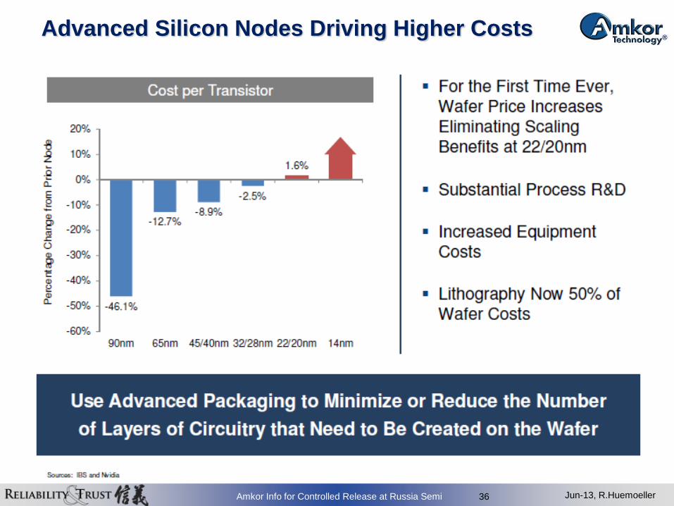
Advanced Silicon Nodes Driving Higher Costs

Jun-13, R.Huemoeller 37 Amkor Info for Controlled Release at Russia Semi
Logic SoC
Logic 1
Logic 3
Logic 2
Logic 4
• Focus Process Node Development on Specific Application Functionalities
Reduces complexity and mask layer count of process node
Improves wafer yield
Reduces wafer start cost
Improves performance, power, and area of each application
Multi-Die
Interposer
SiP
Monolithic
22nm SOC
Type 1
Multi-Die
Interposer
SiP
Monolithic
22nm SOC
Type 2 SoC
Logic 1
Logic 1
Cache
Logic 2
Logic
1
Logic
2
Cache
Analog
Lo
gic
1
Lo
gic
2
Logic
3
Lo
gic
4
SoC Logic 1
Analog Logic 2
SOC to 2.5D TSV MCM SiP Drivers
Jun-13, R.Huemoeller 38 Amkor Info for Controlled Release at Russia Semi
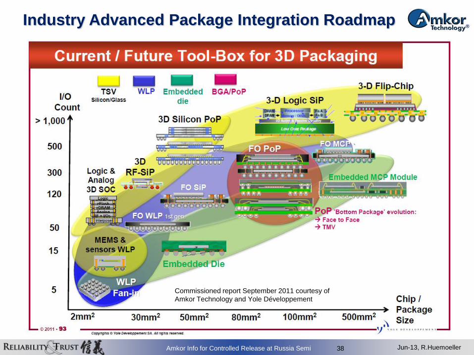
Commissioned report September 2011 courtesy of
Amkor Technology and Yole Développement
Industry Advanced Package Integration Roadmap
Jun-13, R.Huemoeller 39 Amkor Info for Controlled Release at Russia Semi
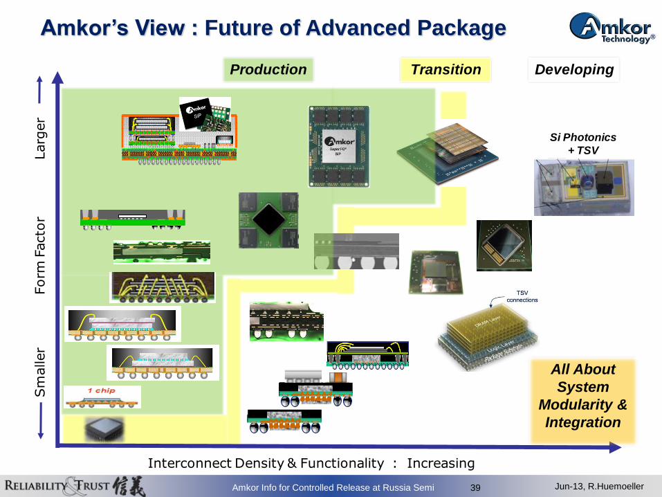
Amkor’s View : Future of Advanced Package Sm
aller F
orm
Facto
r Larg
er
Interconnect Density & Functionality : Increasing
Production TransitionDie
Developing
Die
Si Photonics
+ TSV
All About
System
Modularity &
Integration

Enabling a
Microelectronic
World®
Thank You!


