The impact of Ill-V semiconductors on microelectromechanical systems by R. C. Woods and A. L. Powell This article examines the special-fiatures ofthe III- V semiconductors, such as gallium arsenide and chemically related compounds, which make them an attractive alternative to silicon-based technology in thefield of microelectromechanical systems. As in conventional electronic systems, it is not expected that the III- V compounds will become exclusively used in all instances, but rather a substantial niche market-exploiting the special advantages of the compound semiconductors-is likely to be established. Introduction o far, the vast bulk of the research worldwide in the field of microelectromechanical systems , (MEMS) has been performed by laboratorie5 using silicon-based processing techniques. The precise reasons for this appear to have been, to some extent, historical. It is true that silicon offers some desirable features when used as a substrate for certain types of micromachines, mainly dependent on favourable mechanical properties such as its relatively high yield stress and Young’s modulus, when used in single-crystal form as readily available to the micro- electronics industry. Nevertheless, semiconductors in the 111-V compound family (made from elenients in group 111 and group V of the periodic table, such as GaAs, InP, InSb, Ids, U s , Gap, Ale and intermediate alloy compositions) have other, comple- mentary advantages which will increasingly be harnessed effectively in the future in the MEMS field. The Sheffield Ill-V technology base Epitaxial growth of 111-V compounds within the Department of Electronic and Electrical Engineering at the University of She5eld dates from 1972, whilst 111-V device work has been carried out in the Department since the 1960s. The Sheffield Central Facility for 111-V Semiconductors was founded in the Department by the Science and Engineering Research Council (SEKC) in 1978. Its primary role is to develop 111-V technolog, to assist with the fabrication of appropriate devices, and to supply 111-V semiconductor materials to UK universities (including She5eld). Work can also be undertaken for commercial and other research organisations. Currently, two metal-organic vapour phase epitaxy (MOVPE) and two molecular beam epitaxy (MBE) reactors (Fig. l), combined with the extensive fabrication (Fig. 2) and assessment facilities (Fig. 3), provide a wide range of state-of-the-art material systems, structures, and devices. MOVPE and MBE are the leading methods of deposition of epitaxial layers of 111-V semiconductors; other techniques, such as cheniical beam epitaxy (CBE) and the established method of liquid-phase epitaxy (LPE), are also available. These techniques make feasible the precise control of semiconductor layer thicknesses, by depositing materials closely related to GaAs which have properties sufficiently different that they can be distinguished using chemically active etching processes (either wet or dry). Control of the laycr deposition to within one monatonlic (single atom) layer of semiconductor is now routine. This could lead to extremely fine scale engineering of mechanical structures, a possibility which so far has not been seriously addressed by the MEMS conlmunity. The full details of these deposition techniques are comprehensively described in many places elsewhere. Although much ofthe traditional expense of setting up ENGINEERING SCIENCE ANI1 EIIUCATION JOURNAL DECEMBER 1994 27 1
Transcript
The impact of Ill-V semiconductors on microelectromechanical systems by R. C. Woods and A. L. Powell This article examines the special-fiatures ofthe III- V semiconductors, such as gallium arsenide and chemically related compounds, which make them an attractive alternative to silicon-based technology in the field o f microelectromechanical systems. As in conventional electronic systems, it is not expected that the III- V compounds will become exclusively used in all instances, but rather a substantial niche market-exploiting the special advantages o f the compound semiconductors-is likely to be established.
Introduction
o far, the vast bulk of the research worldwide in the field of microelectromechanical systems , (MEMS) has been performed by laboratorie5 using silicon-based processing techniques. The
precise reasons for this appear to have been, to some extent, historical. It is true that silicon offers some desirable features when used as a substrate for certain types of micromachines, mainly dependent on favourable mechanical properties such as its relatively high yield stress and Young’s modulus, when used in single-crystal form as readily available to the micro- electronics industry. Nevertheless, semiconductors in the 111-V compound family (made from elenients in group 111 and group V of the periodic table, such as GaAs, InP, InSb, I d s , U s , Gap, Ale and intermediate alloy compositions) have other, comple- mentary advantages which will increasingly be harnessed effectively in the future in the MEMS field.
The Sheffield Ill-V technology base
Epitaxial growth of 111-V compounds within the Department of Electronic and Electrical Engineering at the University of She5eld dates from 1972, whilst 111-V device work has been carried out in the Department since the 1960s. The Sheffield Central Facility for 111-V Semiconductors was founded in the Department by the Science and Engineering
Research Council (SEKC) in 1978. Its primary role is to develop 111-V technolog, to assist with the fabrication of appropriate devices, and to supply 111-V semiconductor materials to UK universities (including She5eld). Work can also be undertaken for commercial and other research organisations. Currently, two metal-organic vapour phase epitaxy (MOVPE) and two molecular beam epitaxy (MBE) reactors (Fig. l), combined with the extensive fabrication (Fig. 2) and assessment facilities (Fig. 3) , provide a wide range of state-of-the-art material systems, structures, and devices.
MOVPE and MBE are the leading methods of deposition of epitaxial layers of 111-V semiconductors; other techniques, such as cheniical beam epitaxy (CBE) and the established method of liquid-phase epitaxy (LPE), are also available. These techniques make feasible the precise control of semiconductor layer thicknesses, by depositing materials closely related to GaAs which have properties sufficiently different that they can be distinguished using chemically active etching processes (either wet or dry). Control of the laycr deposition to within one monatonlic (single atom) layer of semiconductor is now routine. This could lead to extremely fine scale engineering of mechanical structures, a possibility which so far has not been seriously addressed by the MEMS conlmunity. The full details of these deposition techniques are comprehensively described in many places elsewhere. Although much ofthe traditional expense of setting up
ENGINEERING SCIENCE ANI1 EIIUCATION JOURNAL DECEMBER 1994
27 1
Fig. 1 This equipment is used for depositing ultra-thin epitaxial films of Ill-V semiconductors
a processing house for 111-V semiconductor devices is concerned with these epitaxial techniques, the costs There are obvious intrinsic advantages in using a incurred in establishing a basic capability can be material which is naturally tailored for optical minimised by collaboration with a third party such as applications’ since devices made from it will be easily the MEMS Unit at Sheffield, which interfaced with other mainstream has strong links with the 111-V Central optical technologie5 such as fibre- Facility. optics. The latter provides high
immunity to electromagnetic Advantages given by interference and relatively few EMC material properties of Ill-V problems so that the associated compounds security is high and interchannel
crosstalk low. There is also the Clearly, one major advantage of the possibility of exploiting the electrical 111-V materials will be that of optical isolation between different MEMS activity. Silicon has an indirect energy subsystems, and the possibility of gap, whose value is 1.12 eV at mom wide-bandwidth optical con- temperature; these two facts niunications both inside and outside effectively have ruled out the use of the complete system of which the silicon for optoelectronic applications, MEMS is a component. (Integrated because it is difficult to adjust the 111-V electronic active devices are also energy gap to a value which is technologically ideal for such systems as they offer a significant speed important for fibre-optical applications (although one new method of doing this is to use ‘porous silicon’ A further natural advantage, which is important prepared by a special etching technique which is still in in certain specialised tnarkets, is that the 111-V its infancy). By contrast, GaAs has a direct energy gap semiconductors generally have a relatively low defect of value 1.42 eV at room temperature’, corresponding generation rate when subjected to high-energy to optical activity at a wavelength of h = 0.9 pm. The ionising radiation, in contrast to silicon in which defect other 111-V compounds have differing energy gaps and generation rates are much higher under similar can be utilised for applications requiring different conditions. This means that silicon devices malhnction optical wavelengths, ranging from the infra-red a t under such conditions whereas an equivalent 111-V
Molecular-beam epitaxy equipment at the Central Facility for Ill-V Material Growth at the University of Sheffield
1.5 km to the visible red at around 0.7 pm.
increase over equivalent silicon devices.)
ENGINEERING SCIENCE AND EDUCATION JOURNAL DECEMBER 1994
272
device will not be subject to failure. Because of this, circuit designs using these materials have for some years been contenders in applications subject to high doses of radiation where reliable operation is essential and safety-critical. These applications include control systems in nuclear power plants and some aerospace applications.
Other potential advantages from using the Ill-V semiconductors arise from the ease of integration of a MEMS sensor device together with closely associated circuitry, e.g. recovery amplifiers, zero offsetting, bandwidth limiters, frequency-lock subsystems, linearisers, analogue and dlgital signal-processors, analogue-to-dlgital and dgital-to-analogue converters, control circuimy, and microprocessor subsystem control, as needed in any particular design example. T h s would turn a basic sensor into a ‘smart’ sensor (which can be interfaced easily with external subsystems without the high-end system controller needmg to be concerned with device-specific measurement techniques), and should be possible using either silicon or Ill-V technology. The advantages of such a monolithic approach will, in many cases, far outweigh the &sadvantages ofthe constraints placed on the design by whichever of the micromechanical device or the bundled circuitry is less well suited to the technology chosen. However, the unprocessed and unamplified signals from a typical microminiaturised sensor wdl be extremely small in amplitude. Lower noise figures can be obtained using integrated circuitry based upon 111-V technology, and therefore circuitry fabricated using such low-noise 111-V technology can more easily handle the available signals with accuracy
Although the integration scales currently achievable using Ill-V semiconductors are not as large as with silicon, unless an extremely complex on-board processing system is required then current 111-V technology is able to handle the typical requirements of most smako-medium scale ‘smart’ sensor system5. In
many cases the smaller integration scales possible using III-V technology will be ofiet by the much greater speed of operation of the Ill-V devices compared to silicon devices; this is often a significant reason for choosing Ill-V based electronic circuitry in applica- tions w h c h are otherwise conventional. Using 111-V based circuitry also enables full advantage to be taken of the possibhties ofwide-bandwidth communications to the other system components.
In addition, the use of MEMS structures as an incidental feature in an otherwise conventional 111-V design should not be forgotten. For example, the use of microfabricated switches in a design with built-in redundancy4 points towards further useful future developments.
Advantages offered by the unique processing capabilities of Ill-V compounds
Current MEMS structures appear to fall into one of two broad categories:
(a) those produced on the surface of the substrate material via the deposition and patterning of additional compounds to build the required MEMS structure; and
(b) those produced primarily by etching the surface of the substrate material to create the desired physical structure below the level ofthe initial top face ofthe sample.
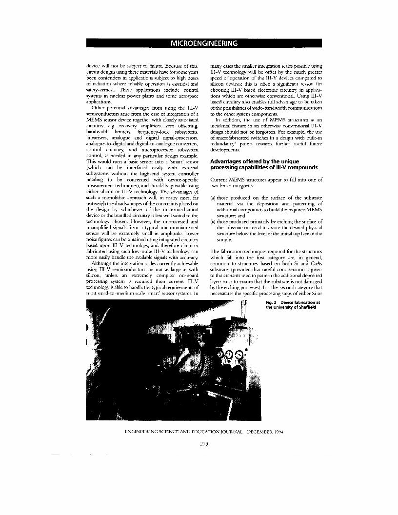
The fabrication techniques required for the structures which fall into the first category are, in general, common to structures based on both Si and GaAs substrates (provided that careful consideration is given to the etchants used to pattern the additional deposited layers so as to ensure that the substrate is not damaged by the etching processes). It is the second category that necessitates the specific processing steps of either Si or
Fig. the
2 Device University
!fabrication at of Sheffield
ENGINEERING SCIENCE ANI1 EI)UCATION JOURNAL DECEMBER 1994
273
~~ ~
Fig. 3 Optical device assessment at the University of Sheffield
111-V based technologies. Although Si based processing technology is currently considered the norm for MEMS fabrication, some of the unique properties of the competing 111-V technology should not be disregarded’-’. The relative ease of depositing epitaxial 111-V semiconductor layers (using techniques such as MOVPE or MBE) with differing chemical and/or electrical properties, combined with precise control of layer thicknesses, enabler coniplex structures to be etched using simple selective chemical etching procedures with accuracies of the order of a few nanometres. A typical cantilever structure (supported at one end as required, for example, for an accelerometer design), a suspended beam (supported at two opposite ends), or a suspended membrane (substantially supported on all sides) can then easily be produced using sacrificial etching.
Equally, there are some processing steps which can more effectively and efficiently be carried out using Si based technology However, the conflicting demands of the two competing technologies in terms ofthe capital plant investment and safety precautions, which are in several important aspects difficult to combine within a single clean-room complex, result in the fact that generally the two technologies cannot easily be mixed in the same device. It therefore follows that either a predominantly silicon based or a predominantly 111-V based approach must be used for any one particular device structure, and it will probably be difficult to use the two technologies within one device. The characteristics, function, and operation of the intended structure must be the final arbiter of the preferred technology route.
Finally, two specialired techniques should be mentioned which combine the advantages ofGaAs and Si semiconductorsx. Although Si and 111-V technology do not easily mix, nevertheless a number oflaboratories worldwide (notably AT&T Bell Laboratories) have been involved in the growth of GaAs epitaxial layers on
silicon substrates. This technology attempts to combine the relatively low cost ofsilicon substrates with the high electrical pe*brmance ofdevices fabricated using GaAs epitaxial layers. The alternative technique of epitaxy lift-off, pioneered at the University of Ghent, attempts to achieve the same result; essentially a suitable 111-V device structure is produced conventionally and then freed from its native substrate by sacrificial etchmg. It is then possible to transfer the thin-fdm epitaxial layers, as one entity forming the 111-V semiconductor device, to a separate silicon wafer. The thin layers malung up the 111-V device are held in place by van der Waals forces alone, which in most applications are sufficient for effective bonding because of the small mass of the transferred device structure and the close fit possible between the silicon wafer and 111-V structure.
Currently neither of these techniques is widely available, but they are expected to increase in importance rapidly as other laboratories gain relevant experience as they offer the first practical method of combining the two main (and normally mutually exclusive) semiconductor technologies in one structure. Their dlsadvantage, at the moment, is that their use is highly labour-intensive and so in production they will be extremely expensive unless they can be automated to a significant degree.
Conclusions
Although much of current research work in MEMS is directed towards the realisation of microscopic electromechanical structures in silicon, in certain cases there will be advantages in using one of the 111-V semiconductors instead. Generally spealang, the level of integration possible now using 111-V technology is less than the level of integration possible using silicon, but the currently attainable integration standards should still be adequate for typical MEMS applications such as ‘smart’ sensors. However, the actual processing
ENGINEERING SCIENCE AND EDUCATION JOURNAL DECEMBER 1994
271
steps for 111-V compounds have been highly developed over the last twenty years or so and in many cases will be more suitable than silicon technology for,the fabrication of microstructures. The intrinsic and unique material properties of 111-V semiconductors may give another good reason for using this material group rather than silicon. The Sheffield MEMS Unit, together with the Sheffield 111-V Central Facility, has in-house access to all ofthe process techniques required for microfabrication using 111-V materials, and is actively involved in worlung with external organisa- tions on all aspects of the development of 111-V processes, devices, and applications.
Acknowledgments
It is a pleasure to acknowledge many helpful discussions with the other members of the MEMS Unit at Sheffield, and in particular Professor I . L. Freeston, Professor C. R. Whitehouse, Dr. J. Woodhead and R. B. Yates. The Sheffield University MEMS Unit is supported by the New Academic Developments Fund of the University of Sheffield. The photographs are by Sonya Saxby.
References
1 Japanese Ministry of International Trade and Industry (MITI), 1990
2 ADACHI, S.: ’GaAs, A I A s , and Al,Gal-,As: Material para- meter5 for use in research and device applications’, J Appl. Phys., 1985, 58, pp.Rl-R29
3 DElMEL, E E: ‘Micromachining processes and structures in micro-optics and optoelectronics’, J Micromerhaniu G Micro- engineering, 1991, 1, pp.199-222
4 DRIVER, M. C., NATHANSON, H. C., FREITAG, R., ELDRIDGE, G. W., CLARKE, R. C., and SOPIRA, M. M.: ‘Wafer scale integration’. Proc. IEEE/Cornell Conf. on Adv. Concepts in High Speed Semiconductor Devices and Circuits, 1-1, 1989, pp.1-10
6 HJORT, K., SCHWEITZ, J.-A., and HOK, B.: ‘Bulk and surface nucromachining of GaAs structures’. Proc. IEEE MEMS Conf., 1990, pp.7S76
7 ZHANG, Z . L., and MACDONALD, N. C.: ‘Fabrication of submicron high-aspect-ratio GaAs actuators’, I € € € J .MEMS, 1993, 2, pp.6h-73
8 DEMEESTER, P, ACKAERT, A., GOUDENSYS, G., MOERMAN, I . , BWDENS, L., POLLENTIER, I . , and VAN DAELE, P: ‘Relaxed lattice-mismatched growth of 111-V semiconductors’. Pro,. Cryst. Growth Charact. Mater, 1991.22, pp.53-141
OIEE 1994
Dr Woods and Dr Powell are with the MEMS Umt within the Department of Electronic and Electrical Engineering, University of Sheffield, Mappin Street, Sheffield, S1 3JD. United Kngdom
This is a free listing. Please send details of events for possible inclusion to the Staff Editor, Engineering Science and EducafionJoumal, IEE, Michael Faraday House, Six Hills Way, Stevenage, Herts. SGl 2AY, UK.
*Unless otherwise stated, IEE colloquia, meetings and lectures are held at Savoy Place, London. Further details are available from the Secretary, IEE, Savoy Place, London WC2R OBL, quoting the reference LS(D)CA, or by telephoning 071-240 1871.
Readers are advised to confirm details with the event organisers
12th January 1995 French Conversation Circle. IEE SET Division SlO/EIFLG meeting*
12th January 1995 Reflections in Appleton’s Mirror-A Century of
Ionospheric Science. IEE 30th Appleton Lecture by Professor H. Rishbeth (University of Southampton)*
18th January 1995 Tomography-Calibration and Accuracy in Tomographic Measurement. IEE SET Division S4 Discussion Meeting at the University of Leeds. Free admission by ticket only from the Secretary, IEE, Savoy Place, London WC2R OBL, quoting Ref. LS(D)CA
18th January 1995 The History of Post-War Radar. IEE PGs S7 and E15 Lecture by Mr. D. Todin*
BLUMLEIN MEMORIAL LECTURE
19th January 1995 The Magic of Radio and its Musical Heritage-a chronological kaleidoscope of some of the finer moments from BBC Radio and the UK music industry; Erom the earliest recordings in the BBC’s Sound Archives, through the first stereo experiments of the 1930s, World War 11, rock ’n roll, the 45, the microgroove LP, the stereo LP, VHF and the cultural shift to ‘stereo FM’. IEE SET Lecture by Mr. D. Price (BBC)*
19th January 1995 Applications of Digital Recording and Measurement Equipment. IEE PGs P7, P11 and S4 Discussion Meeting*
24th January 1995 Chambres de Commerce en France et en Grande-Bretagne Vive la Difference. IEE SET Ilivision SlO/EIFLG Lecture in French by Mr. P H. South*
ENGINEERING SCIENCE AN11 EDUCATION JOURNAL DECEMBER 1Y94