The Impact of Nitrogen for a Robust High Yield Soldering Process The Impact of Nitrogen for a Robust High Yield Soldering Process Denis Barbini, Ph.D. Associate Director of the Advanced Process Laboratory Denis Barbini, Ph.D. Associate Director of the Advanced Process Laboratory
Transcript
The Impact of Nitrogen for a Robust High Yield Soldering Process
The Impact of Nitrogen for a Robust High Yield Soldering Process
Denis Barbini, Ph.D.Associate Director of the Advanced Process Laboratory
Denis Barbini, Ph.D.Associate Director of the Advanced Process Laboratory
About the PresenterAbout the Presenter
Denis is the Associate Director of the Universal Instruments’ Advanced Process Laboratory. He started his career in the electronics manufacturing world after earning his Doctorate in Chemistry from Binghamton University. His current focus is identifying the critical needs in emerging technologies and electronics assembly processes in order to
develop specific research and development projects. Denis has authored hundred’s of peer reviewed articles, several books and presented to thousands of his peers on the results of his research over the past 15 years.
Denis volunteers his time serving on the board of the Surface Mount Technology Association. For the past 7 years, his focus is on implementing new programs that deliver leading edge technology
solutions for the user and speaking at SMTA chapter events all over the world.
Advanced Process LaboratoryAdvanced Process Laboratory
Binghamton, NYBinghamton, NY
Founded in 1987
• First and most complete Advanced Process Laboratory in the industry generally accessible to customers
APL is made up of 3 interactive groups
• Area Consortium
• Process Support
• Failure Analysis
Founded 1st Consortium - 1992
Complete Analytical Laboratory
Full process development and production capability
ITAR Compliant
ISO 9001 Certified
A.R.E.A. Consortium
Failure
Analysis
Process
Support
Soldering 5500 years ago
Egyptian Tomb Thebe, Egypt Dated: 1475 BC
Joining of tools and ornamentals
Alloys:AuCu, AgCu and PbCu(Hard soldering >300 C)
Roman Soldering Technology - 2000 Years Ago
Romans introduced SnPb for soldering lead sheets together for transporting water in the aquaducts.
Cu and Au also used
Vitruvius:
“Water conducted through earthen pipes is more wholesome then through lead”
Soldering Technology - 2001 A.D.
Highly sophisticated process controls and optimization of process
based on materials used.
Today’s Agenda
The assembly yield of a specific electronic PCB will depend on the
interaction of two variables:
• Materials
• Process
This presentation will focus on the use of nitrogen in solderingprocesses.
•A look at Materials and the Impact of Nitrogen
•Case Study 1 – The impact of nitrogen on OSP and Optimized Processes for the Hole Fill
•Case Study 2 – The impact of nitrogen in the assembly process for a Package on Package
•Case Study 3 – The Impact of Nitrogen on the assembly process for 01005
Quality in Today’s Market
Notebooks and Laptops
Source: Consumer Reports
Materials and the Impact of Nitrogen
Content
Impact of materials on going to higher temperatures:Profile
AlloysPasteExperiments on materials with the use of nitrogen
Lead-Free Profiles: Ramp Soak Spike
Due to the higher temperatures and longer time, there is a greater chance for oxidation of metal surfaces.
Ternary Eutecticcomposition:Sn - 3.5 Ag - 0.9 Cu Melting point: 217°C
All alloys in the green area have a melting range <10°C.
Impact on materials:Solderpaste particle sizes
DIN 32 513:85% minimum between 20 and 45 µm.
10% maximum between 15 and 25 µm.
3% maximum < 15 µm.
3% maximum between 45 and 50 µm.
None larger than 50 µm.
J-STD-005:80% between 25 and 45 µm.
10% maximum < 10 µm.
Less than 1% larger than 45 µm.
None larger than 50 µm.
USL = 50 µmLSL = 10 µm
Cp = 1.45
10 types of solder paste evaluated.
Flux Compatibility Issues
Reflow Profiles are designed around material restrictions such as component, board, and flux specifications. Deviations from the recommended specifications can result in solder defects.
Determine to Use Air or Inert Atmosphere
Lab tests shows improved wetting, SnAgCu paste
Advantage:
• Nitrogen will improve wetting
Disadvantages:
• Costs
• Tombstone defects
Tsol* Tliq
(ºC) (ºC) Air Nitrogen
Sn (pure) 232
Sn-37Pb 183 417 464
Sn-3.5Ag 221 431 493 Ag3Sn
Sn-4Cu-0.5Ag 216 222 Ag3Sn, Cu6Sn5
Sn-0.7Cu 227 491 461 Cu6Sn5
Sn-58Bi 138 319 349
Sn-9Zn 199 518 487
Judith Glazer, “Microstructure and Mechanical Properties of Pb-free Solder
Alloys for Low-Cost Electronic Assembly: A Review,” J. Electronic Materials
Surface Tension
(at Tliq + 50 ºC)
(mN/mm) Intermetallic
Phases
Alloy
Nitrogen Impact on Surface Tension
Wettability Tests and Analysis
Nitrogen improves wetting.
Nitrogen protects board finishes through multiple reflow passes.
Nitrogen does not remove the micro-cracks of the SnAgCu surface.
Nitrogen increased thombstone risk.
Less oxidation on the Cu coupon.
Levels of 500 to 1000 ppm are normally sufficient to let the flux perform well.
Nitrogen (some dewetting visible)
Air (Cu more discoloured)
Nitrogen and Spreading
Solder spread test.
Sn3.5Ag0.75Cu
With nitrogen the spread
characteristics of the lead-free solder paste improves.
Air Nitrogen
Nitrogen and Solder Ball Test
Solder balling test on ceramic.
Sample 7: Sn3.0Ag0.5Cu
No significant differences in between air and nitrogen atmosphere.
The nitrogen prevents however
oxidation of the surfaces that need to be soldered.
Air
Nitrogen
Nitrogen and Miniaturisation
No-clean lead-free solder pastes are compatible to solder in
air atmosphere.
Bad coalescence of lead-free solder paste reflowing small solder paste deposits, e.g. fine pitch flip chip, 0201 and smaller.
Corrective action:
Use nitrogen, or
Apply more solder paste.
Small solder deposits, so
activators will evaporate fast.Oxidation of solder balls.
ConclusionsConclusions
Nitrogen has a positive effect on :
•Improving the wetting of the paste to pads and component terminations.
•Decreases the wetting angle
•Improves the flux residue left behind after the reflow process.
•Improves the coalescing of the particles in the solder paste.
•Improves the spreading of the paste on copper pads.
•Ultimately, nitrogen prevents the formation of metal oxides on the surfaces of the pads, components terminations/bumps/leads and paste
allowing for improved yields.
Case Study 1 – The Impact of Nitrogen on OSP and Optimized Processes for the Hole Fill
Case Study 1 – The Impact of Nitrogen on OSP and Optimized Processes for the Hole Fill
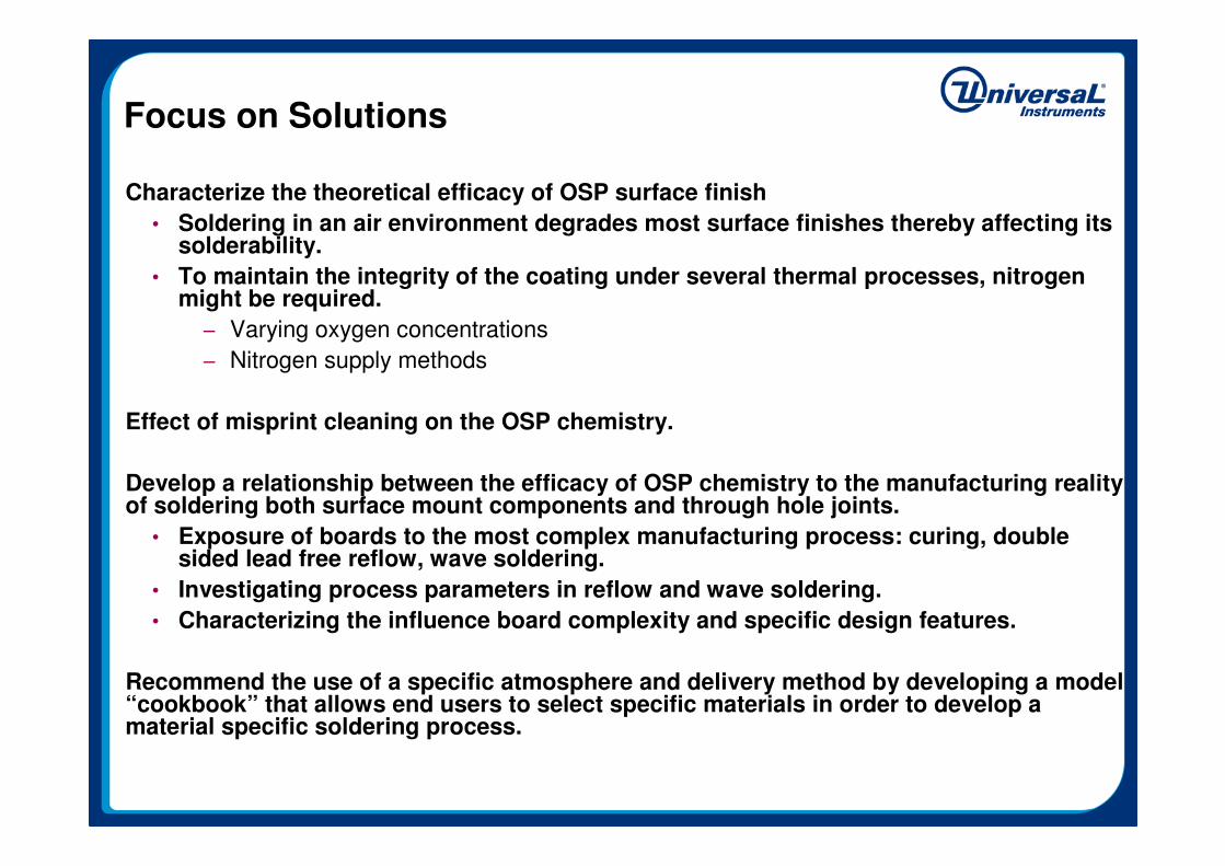
Focus on Solutions
Characterize the theoretical efficacy of OSP surface finish
• Soldering in an air environment degrades most surface finishes thereby affecting its solderability.
• To maintain the integrity of the coating under several thermal processes, nitrogen might be required.
– Varying oxygen concentrations
– Nitrogen supply methods
Effect of misprint cleaning on the OSP chemistry.
Develop a relationship between the efficacy of OSP chemistry to the manufacturing reality of soldering both surface mount components and through hole joints.
• Exposure of boards to the most complex manufacturing process: curing, double sided lead free reflow, wave soldering.
• Investigating process parameters in reflow and wave soldering.
• Characterizing the influence board complexity and specific design features.
Recommend the use of a specific atmosphere and delivery method by developing a model “cookbook” that allows end users to select specific materials in order to develop a material specific soldering process.
Why Manufacturers Use OSP
Increase popularity due to lead free requirements.
Cost effective.
Proven solder joint reliability.
• What you see is what you get.
Temporary layer of protection from oxidation of the Cu surface.
OSP is penetrated and dissolved by flux and temperature.
Able to withstand multiple thermal excursions such as reflow, wave, and rework processes.
28%
17%
14%37%
4%
OSP
Imm Ag
ENIG
HASL
Imm Sn
Source: Van Der Pas, F., Yau, Y., Wengenroth, K., and Kenny, J., “Selecting the Right Final Finish for ROHS
Compliant PCBs,” Printed Circuit Design and Manufacture, March 2007, pp 2-5.
Washing Process: change in color - from light brown to dark brown.
Nitrogen Process: no visible difference in color at any oxygen content or profile used.
Air Process: Major differences. Worse discoloration when profile 2 for pre-conditioned boards.
AIR Profile 1
AIR Profile 2
0 W 1 W 2 W
0 W 1 W 2 W
0W 1W 2W
Profile 2 FT 500 O2 ppm
2W0W
Profile 2 RO 500 O2 ppm
1W
Visual Inspection - Impact of…
Impact of Atmosphere on OSP Thickness
Initial OSP Thickness = 0.39 microns
Significant effects of Oxygen Content and Supply Method.
Mean analysis on Profile yields no impact to OSP thickness. However…
2 1 0 0 0 02 5 0 01 2 0 05 0 02 5
0 .2 0
0 .1 9
0 .1 8
0 .1 7
0 .1 6
RF
21
0 .2 0
0 .1 9
0 .1 8
0 .1 7
0 .1 6
O xyg e n Co n t e n t
Mean (Microns)
N2 su p p ly
P ro f ile
Main Effects P lot for ThicknessData M eans - Ze ro W ash
Loss of OSP
Loss of Cu OSP Surface Finish
40
45
50
55
60
65
25 500 1200 2500
Oxygen Content (ppm)
Thic
kness L
oss (%
)
RO - Profile 1
RO - Profile2
Results shown are for Reflow Only atmosphere control.
OSP thickness reduction exhibits a slight effect based on profile.
• Profile temperature exerts an inconsistent loss in OSP.
• Use of an air atmosphere results in the highest consumption of OSP.
Average reduction in OSP thickness 48.4% in N2 and 59.5% in Air.
Less OSP thickness reduction compared to full tunnel configuration.
Impact of Cleaning on OSP Thickness
2100002500120050025
0.04
0.03
0.02
RF
21
0.04
0.03
0.02
Oxygen Content
Mean
N2 supply
Profile
Main Effects Plot for ThicknessData Means - 1 Wash
• Significant reduction in
OSP thickness when
coupons subjected to either
1 or 2 wash cycles.
2100002500120050025
0.04
0.03
0.02
RF
21
0.04
0.03
0.02
Oxygen Content
Mean
N2 supply
Profile
Main Effects Plot for ThicknessData Means - 2 Wash
1 Wash + Reflow
2 Wash + Reflow
Solderability Testing
Solderability testing was performed in order to confirm impact of atmosphere on OSP efficacy.
• BGA Coupons were used to characterize solderability.
– 256 solder pads per coupon.
– 30 mil diameter.
– Solder mask defined pads.
– Coated with Entek Plus HT OSP.
– Six (6) coupons per soldering atmosphere.
• Coupons processed utilizing Profile 2.
• Selected two soldering atmospheres:
– Full tunnel <100ppm O2
– Air
• Coupons were then dipped in a rosin based flux for 1 minute. Post fluxing coupons were individually submerged into molten solder (Sn/3.9%Ag/0.6% Cu) for 5 seconds.
• Coupons were then cooled and rinsed with alcohol.
• Characterization of solderability was accomplished by counting the number of unsoldered pads.
Solderability Results
A total of 1280 opportunities exist from the five BGA coupons.
AIR results
• 41 pads not soldered
• 8.2 ±±±± 5 average defects/board
• 3.2% defects
N2 results
• 17 pads not soldered
• 3.4 ±±±± 2 average defects/board
• 1.3% defects
OSP thickness measurements showed a decrease of 18.5% from coupons processed under <100 ppm O2 versus those processed under ambient conditions.
• This confirms the significance of OSP thickness measurement as a benchmark for the OSP efficacy.
NitrogenAir
14
12
10
8
6
4
2
0
Number of Un-Solderable Pads
Boxplot of Air, Nitrogen
Flextronics Test Board
16 layers, FR4 board
93 and 125 mil thick
Cu OSP: Entek Plus HT
When Theory Meets Reality…
OSP thickness measurements were taken and analyzed. Interactions described. However, OSP efficacy can only be measured by performing various soldering operations under controlled conditions.
This investigation aims to develop a bridge and understanding between the relationship of OSP thickness and through hole penetration.
An identical experimental with no wash cycles was performed utilizing the Flextronics Test Board.
Use of N2 yielded acceptable joints. Air did not.
NitrogenA ir
1.0
0.9
0.8
0.7
0.6
ROFT
2100002500120050025
1.0
0.9
0.8
0.7
0.6
W ave Solde r Ambient
Mean
RO/FT
0.75
ppm leve l
0.75
Main Effects P lot for TH - 125 mil thick Board - Alcohol F lux
64 lead pin connector
Influence of Reflow Atmosphere on Through Hole Penetration – 125 mil
Acceptable hole fill. 75% as per IPC 610D
8642
0.8
0.7
0.6
0.5
0.4
7060 47433935
NitrogenA ir
0.8
0.7
0.6
0.5
0.4
Perpendicu larParallel
Lay ers
Mean
Pad Ho le
0.75
W av e So lder Ambient O rientation
0.75
Main Effect Plot for TH - 125 mil thick Board - A lcohol Flux - 21% - Pin Connector
>75% TH – Air
Hole: 35 mils
Layer: max. 4
Pad: 70 mils
Orientation: Parallel
Can We Achieve Acceptable Joints Under Air Atmosphere?
Yes BUT under specific process conditions and board designs.
Nit rogenA ir
0.93
0.92
0.91
0.90
0.89
AVOC
2100002500120050025
0.93
0.92
0.91
0.90
0.89
ROFT
W ave So lde r Ambient
Mean
Flux
ppm le ve l RO /FT
Main Effect Plot for TH - 93mil thick Boards
Influence of Reflow Atmosphere on Through Hole Penetration - 93 mil
• Both N2 and Air yield acceptable joints.
Effects of Process Parameters
Mean of Solder Rise by Slice
SN100SA C XSA C305
60
40
20
O SPHASL 10 6.04.53.0
321
60
40
20
321 321 10
275265255
60
40
20
DCBA 21
A lloy Brd F in A tmosphere C onv ey or Speed
Preheat F lux Q uantity F lux Ty pe C hip Wav e
Solder Temp Ground Pin C ode
Main Effects Plot - Solder Rise by Slice 0.062" Boards
Mean of Solder Rise by Slice
SN100SA CXSAC 305
50.0
47.5
45.0
O SPHA SL 10 6.04.53.0
321
50.0
47.5
45.0
321 321 10
275265255
50.0
47.5
45.0
DCBA 21
A lloy Brd F in A tmosphere C onv ey or Speed
Preheat F lux Q uantity F lux Ty pe C hip Wav e
Solder Temp Ground P in C ode
Main Effects Plot - Solder Rise by Slice 0.094" Boards
Mean of Solder Rise by Slice
SN100SAC XSA C 305
48
40
32
OSPHA SL 10 5.03.52.0
321
48
40
32
321 321 10
275265255
48
40
32
DCBA 21
A lloy Brd F in A tmosphere C onv ey or Speed
Preheat F lux Q uantity F lux Ty pe C hip Wav e
Solder Temp Ground P in C ode
Main Effects Plot - Solder Rise by Slice 0.135" Boards
++oPin Complexity
+++Solder Temperature
+o-Chip Wave
+o+Flux Type
+++Flux Quantity
+-+Preheat
++oConveyor Speed
+--Atmosphere
o+-Board Finish
++OAlloy
0.1350.0940.062
Source: iNEMI Wave Soldering Project
Findings
The reflow soldering ambient has a significant effect on the degradation of OSP thickness. After 2 reflows, the thickness is reduced by an average of 50.6% under N2 conditions versus 59.5% under ambient conditions.
For the solderability test, coupons reflowed in air were characterized having less solderability compared to those reflowed in N2.
Coupons subjected to the washing and reflow cycle(s) were characterized having OSP thickness reduction of up to 90%.
Use of N2 in reflow process for 125 mil thick Cu OSP boards is necessary to achieve > 75% T/H penetration. For 93 mil thick boards, N2 is beneficial but not necessary.
As for materials,
• The alcohol based flux was more robust than the VOC free flux.
• Optimal T/H design depends on component types.
Summary and ConclusionsSummary and Conclusions
0.1
0.12
0.14
0.16
0.18
0.2
0.22
25 500 1200 2500 210000
Oxygen Content (ppm)
OS
P T
hic
kn
ess (
mic
ron
s)
50.0%
55.0%
60.0%
65.0%
70.0%
75.0%
80.0%
85.0%
90.0%
95.0%
100.0%
T/H
Pen
etr
ati
on
(%
)
T/H Penetration
OSP Thickness
Material Impact on Through Hole Penetration
Materials are affected by the process that
they are exposed to.
Yield is directly
affected.
It is possible to model through-hole penetration
based on process attributes and
material selection.
BOTTOM LINE
Use of some N2 exerts a positive influence on OSP thickness, efficacy, and ultimately joint formation.
&Ensure your printing process is accurate and precise to avoid the
need for washing misprints.
Case Study 2 - The impact of nitrogen in the assembly process for a Package on Package
Case Study 2 - The impact of nitrogen in the assembly process for a Package on Package
Project
Background:
Stacked package technology allows for ever increasing functionality coupled with miniaturization. Through-molded-via PoP provides opportunity for much better warpage control, often a limiting factor in stacked package assembly.
Scope:
To evaluate the process and materials for robust 0.4mm pitch TMV PoP assembly.
Specifically evaluate multiple dip materials and reflow atmosphere for good soldering.
•Metrics:
• Assembly yields and Solder joint Formation
• Reliability
– Drop/shock (JEDEC JESD22-B111)
– Temp Cycling (-40/125 °C)
Through-Molded Via
Traditional “flange” style PoP.
• Bottom package overmold is concentrated at center of device,
with pads for top package soldering.
Through-Molded Via
Traditional “flange” style PoP.
• Bottom package overmold is concentrated at center of device,
with pads for top package soldering.
TMV Style PoP
• Bottom package overmold extends to edges of package
Through-Molded Via
Traditional “flange” style PoP.
• Bottom package overmold is concentrated at center of device,
with pads for top package soldering.
TMV Style PoP
• Bottom package overmold extends to edges of package
• Vias in the overmold are necessary for connection of the top package
Through-Molded Via
Traditional “flange” style PoP.
• Bottom package overmold is concentrated at center of device,
with pads for top package soldering.
TMV Style PoP
• Bottom package overmold extends to edges of package
• Vias in the overmold are necessary for connection of the top package
• Solder balls provide the via fill
*Illustration does not necessarily represent actual product of TMV technology
TMV Assembly
• Assembly process requires attachment of solder ball to solder ball
• Top Package must be dipped into flux or solder paste
• Sensitive to Material Selection
Potential site for non-
coalescing
Test Vehicle
Amkor TMV Components
• Bottom Package: TMVPSvfBGA
– 620 I/O
– 0.4mm pitch
– SAC125Ni
• Top Package: SCSP 200LD
– 200 I/O,
– 0.5mm pitch
– SAC105
TMV structuresTMV structures
Test Board
Standard layout per JEDEC drop/bend methods.
0.8mm thick
4-layer
CuOSP & ENIG versions
NSMD Pads
• 8.2 mil actual diameter
3 daisy chain nets:
• Bottom
• Top Corner
• Top Middle
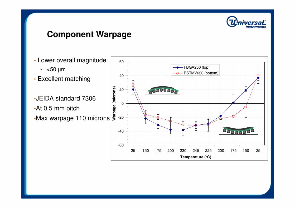
Component Warpage
• Lower overall magnitude
• <50 µm
• Excellent matching
•JEIDA standard 7306
•At 0.5 mm pitch
•Max warpage 110 microns
-60
-40
-20
0
20
40
60
25 150 175 200 230 245 225 200 175 150 25
Temperature (°C)
Wa
rpa
ge
(m
icro
ns
)
FBGA200 (top)
PSTMV620 (bottom)
Postive
Postive
Dipping Materials
•7 Materials were evaluated for top package soldering.
• 2 Fluxes
• 5 Pastes varying alloy, powder and metal content
• 2 Vendors
ID
Material
Type Alloy
Powder
Size
Metal
Content
A Flux, Non-HF -- -- 0%
B Flux, HF -- -- 0%
C Paste, HF SAC305 Type 5 80%
D Paste, HF SAC305 Type 5 80%
E Paste, HF SAC305 Type 5 79%
F Paste, HF SAC305 Type 6 79%
G Paste, HF SAC105 Type 5 79%
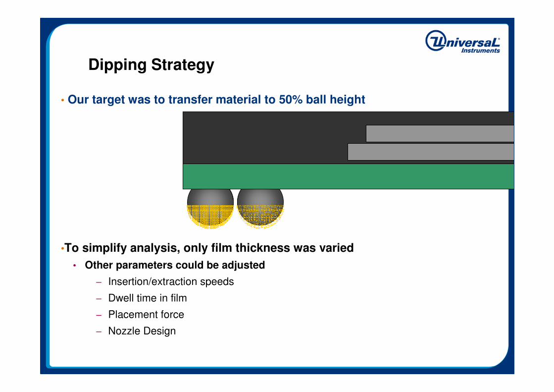
Dipping Strategy
• Our target was to transfer material to 50% ball height
•To simplify analysis, only film thickness was varied
• Other parameters could be adjusted
– Insertion/extraction speeds
– Dwell time in film
– Placement force
– Nozzle Design
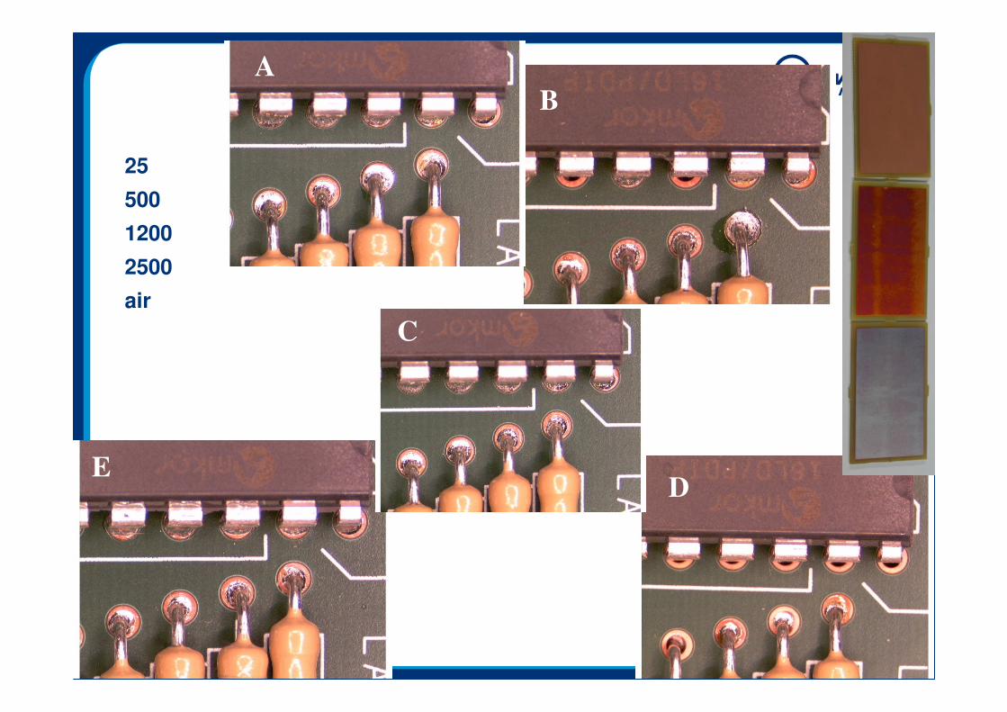
Dip Examples
D
BA
C D
BA
C
30%
40%-50%30%-40%
50%
Flux had no issue achieving 50%
Had to balance thickness with component yield from film
Flux A
Non-HF
Paste C
SAC305 Type 5
Paste F
SAC305 Type 6
Paste D
SAC305 Type 5
Assembly Study
Metrics:
•Component Yields after reflow
• Separated by Bottom and Top Package
•Reflow Conditions
• Average Ramp: 1.0 °C/s
• Peak Temp: 242-245 °C
• Environment
– Air
– N2 (<50 ppm O2)
Assembly Yields
Yields are reported on a per device basis.
30 devices were assembled for each condition
Device
Dip
Material
ID
Material
Type Alloy
Powder
Size
Metal
Content
Number of
Devices
Assembled
Number of
Devices
Open
Yield
A Flux, Non-HF -- -- 0% 30 0 100%
B Flux, HF -- -- 0% 30 0 100%
C Paste, HF SAC305 Type 5 80% 30 12 60%
D Paste, HF SAC305 Type 5 80% 30 14 53%
E Paste, HF SAC305 Type 5 79% 30 25 17%
F Paste, HF SAC305 Type 6 79% 30 25 17%
G Paste, HF SAC105 Type 5 79% 30 17 43%
Bottom All Paste SAC305 Type 5 80 210 4 98%
Device
Dip
Material
ID
Material
Type Alloy
Powder
Size
Metal
Content
Number of
Devices
Assembled
Number of
Devices
Open
Yield
A Flux, Non-HF -- -- 0% 30 0 100%
B Flux, HF -- -- 0% 30 0 100%
C Paste, HF SAC305 Type 5 80% 30 0 100%
D Paste, HF SAC305 Type 5 80% 30 0 100%E Paste, HF SAC305 Type 5 79% 30 0 100%
F Paste, HF SAC305 Type 6 79% 30 0 100%
G Paste, HF SAC105 Type 5 79% 30 0 100%
Bottom All Paste SAC305 Type 5 80 210 0 100%
Top
Top
Air Reflow Atmosphere
Nitrogen Reflow Atmosphere
Assembly Yields
0%
20%
40%
60%
80%
100%
A B C D E F G
Material ID
Asse
mb
ly Y
ield
sAir Reflow N2 Reflow
Defects: Bottom Package
• Bottom device opens were always traced back to insufficient paste transfer
• Defect only observed on assemblies reflowed in air atmosphere using a paste dip process
• Flux dipped process shows much more columnar form of the TMV joint
Paste C: SAC305 Type 5
Air Reflow
Flux A: Non-HF
Air Reflow
Defects were only observed in Air reflow
Defects: Top Package
Paste C:
SAC305 Type 5
Air Reflow
Paste C:
SAC305 Type 5
N2 Reflow
N2 reflow results in more columnar TMV joint: Better coalescing
Defects: Top Package
Paste C: SAC305 Type 5
Air Reflow
Paste C: SAC305 Type 5
N2 Reflow
Defect Analysis
• Flux dipping provides much more flux per volume than paste dipping.
• Flux can easily wet to TMV solder ball during placement.
• Paste provides only limited contact with TMV solder ball
• requires good wetting action to coalesce.
Summary
•TMV assembly is greatly dependent on dip process and materials.
•Standard dip rules apply
• Machine set up is required to optimize material transfer
• Balance quality with throughput
•Air reflow: Better solder joint formation occurs with Flux dipping.
• Flux has better chance to wet to TMV solder ball, better wetting action
• Paste dip has limited flux, poor wetting occurs and “snowman” joints are formed
– Nitrogen required for paste dipping
• Cleaning the TMV device prior to assembly achieved more acceptable yields in air
•N2 reflow: easily achieve 100% yields with all materials tested
Case Study 3 – The Impact of Nitrogen on the Assembly Process for 01005
Case Study 3 – The Impact of Nitrogen on the Assembly Process for 01005
A Challenge Based on Necessity
Chip caps and resistors are among the smallest, simplest and perhaps the least expensive parts in a printed circuit assembly.
However, they require the most attention by perhaps the most expensive investment of the assembly process: the placement machine. Printing and reflow also exert significant influences on the end result.
Developing a process that includes capability for the assembly of 0201 and 01005 components does not have to be a complicated exercise.
Using specific design rules for substrates and stencils, consistent materials, and the proper tools, an acceptable process can be developed.
01005 Component
How small is it?Size Comparison
Grain of SaltGrain of SaltGrain of SaltGrain of Salt
PennyPennyPennyPenny PencilPencilPencilPencil
01005s mixed with black pepper.
Shrinking Footprint
Common Name Capacitor Footprint
(1206) 3216 3.2 mm x 1.6 mm in 1970
(0603) 1608 1.6 mm x 0.8 mm in 1983
(0402) 1005 1.0 mm x 0.5 mm in 1990
(0201) 0603 0.6 mm x 0.3 mm in 1997
(01005) 0402 0.4 mm x 0.2 mm in 2004
•In spite of having equal capacitance the footprint in 1997 is approximately 1/6
of the size in 1990.
And the 01005 has a footprint of 0.08 mm2 vs. 5.12 mm2 of a 1206 capacitor. That is a reduction of 98.5%
The 01005 has a footprint of 44% of that of an 0201.
• Speed, placement accuracy, pick issues, placement order
Reflow: Tolerance to above imperfections?
Not All Components Are created Equally
Capacitor (Murata)
Outline and electrode vary
by each maker.
They can influence
recognition, placement accuracy and pick-up rate.
Resistor (KOA)
Resistor (Matsushita)
Resistor (Hokuriku)
0201 01005
Nozzles
Solder Paste Printing
Type 3 Type 4
Type 5
Pad size: 11x11, 5 mil space between padsAperture size 11x11Stencil thickness: 4 milArea ratio .69
Pad size 8.8 round, .4mm pitchAperture size 9.5 squareStencil thickness 3 milArea ratio .79What if….Stencil 4 mil = .59 ratio
Typical Solder Joint Defects
Component
PCB
Solder joint
Component attachment pad
Component
PCB
Solder joint
Component attachment pad Mis-placed component
Solder paste
Attachment pad
Insufficient solder volume
Excessive solder volume
Component mis alignment
Typical Defects
Open solder joints (tombstone)
Solder beads (solder balls)
Solder bridges
Typical DefectsTombstoning 0201 vs 01005
N2 reflow comparison. Resistors only. Caps may act differently.
Solder Paste Reflow for 01005
�Air or Nitrogen. Process window tighter for Air. The smaller particle sizes required for 01005 oxidize very quickly and easily resulting in a very small process window in an air atmosphere. Nitrogen provides a larger process window.
� Orientation has little effect on defect rates
0201 Experiment Data
Assembly Defects by Attachment Pad Width and Assembly Process Type
0
100
200
300
400
500
600
12 15 18Pad Width (mils)
Nu
mb
er
of
So
lde
r J
oin
t D
efe
cts
No-Clean, Air Reflow
Water-Soluble, Air Reflow
No-Clean, Nitrogen Reflow
0201 Experiment Data
Assembly Defects by Attachment Pad Spacing and Assembly Process Type
0
20
40
60
80
100
120
140
160
180
200
9 12
Attachment Pad Spacing (mils)
Nu
mb
er
of
So
lde
r Jo
int
Fa
ilu
res
No-Clean,
Air Reflow
Water-Soluble,
Air Reflow
No-Clean,
Nitrogen Reflow
Conclusions
Assembly of 01005 components is greatly influenced by materials chosen including: paste type, particle size of the paste, printing parameters, pick and place parameters, and reflow process.
Nitrogen provides the assembler with a larger process window.