39
The Impact of Reduced Solder Alloy Powder Size on Solder Paste Print Performance Presented by Karl Seelig, V.P. Technology AIM Metals & Alloys

The Impact of Reduced Solder Alloy Powder Size on Solder Paste Print Performance
Presented by Karl Seelig, V.P. Technology AIM Metals & Alloys

Solder Powder

Solder Powder Manufacturing and Classification
Type Designation
Mesh Size (lines per inch)
Particle Size, um (at least 80% in range)*
1 150-75 2 -200/+325 75–45 3 -325/+500 45–25 4 -400/+635 38–20 5 -500 25–10 6 -635 15–5 7 11–2 8 8–2

Solder Powder Classification Process
Air Classifier Powder Sieve

45μm 38μm 25μm
Type 3 -325/+500 45-25μm
Type 4 -400/+635 38-20μm
Type 5 -500
25-10μm
Type 6 -635
15-5μm
25μm 20μm
10μm
15μm
5μm
Solder Powder Mesh Size

Powder Types Tested Type 5 Type 4 Type 6

Powder Types Tested
Type 4 Type 5 Type 6

Solder Powder Mesh Size
The “5-Ball Rule”

Print Test
Goal: quantify the benefits and drawbacks derived from smaller particle sizes.
Input variables: Powder size Effect of room temperature storage – Refrigerated and 2 weeks @ room temperature (max. exposure – 80°F/22°C) Pause time – 0-30-60-90 minutes PCB feature types – Mask and non-mask defined pads (Copper) Aperture Shape – Square, Circle, Squircle Output variables: Print transfer efficiency Volume repeatability Performance stability over time

Pad Sizes, Area Ratios and Theoretical Aperture Volumes – 4mil Foil
Pad Size(mil)
AreaRatio
Ap VolCicrle
Ap VolSquare
6 0.38 113 1447 0.44 154 1968 0.50 201 2569 0.56 254 324
10 0.63 314 40011 0.69 380 48412 0.75 452 57613 0.81 531 67614 0.88 616 78415 0.94 707 900
0.4mm BGA 0.63 (sq with 3830.5mm BGA 0.73 rnd corners) 531
For more information on calculating area ratios: Design For Success - Stencil Spec Advisor

Area Ratio and Transfer Efficiency AR = D/4T
Squares & Circles 11.5/(4x4mil)
AR=72
Transfer Efficiency = Theoretical Aperture Volume vs. Solder Deposit
0.004 0.004 11.5 mil

Area Ratio and Transfer Efficiency
Transfer Efficiency = 98%
Aperture Volume
~530 mil3
11.5 mil
520 mil3
0.004 0.004

Solder Mask Defined Pads
11.5 mil
520 mil3
Solder mask defined pads offer more consistent deposits with lower
volume
0.004 0.004
520 mil3

Non-Solder Mask Defined Pad
11.5 mil
577.7 mil3 577.7 mil3
Non-solder mask defined (NSMD) pads offer higher volume with more
inconsistent deposits
0.004 0.004
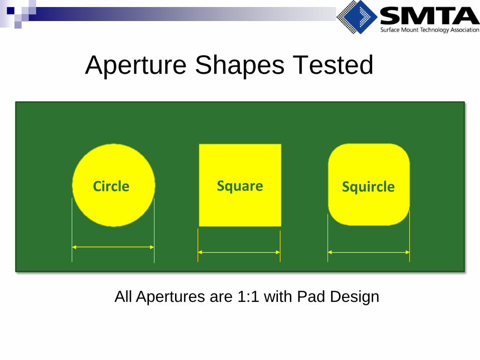
Aperture Shapes Tested
Square Squircle Circle
All Apertures are 1:1 with Pad Design

Test Vehicle
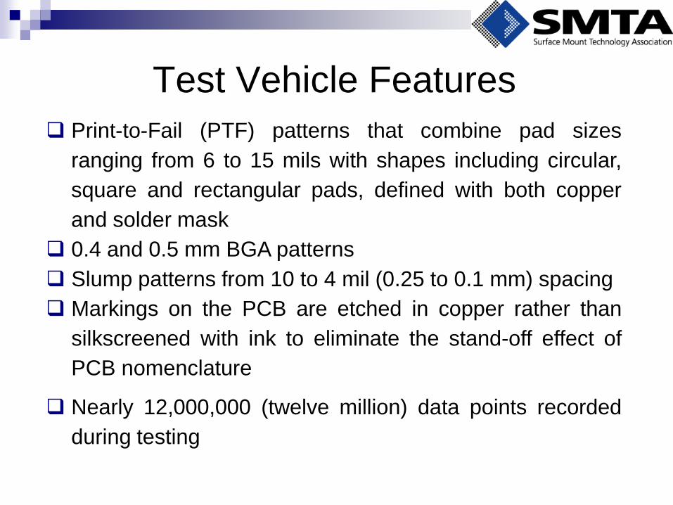
Test Vehicle Features Print-to-Fail (PTF) patterns that combine pad sizes
ranging from 6 to 15 mils with shapes including circular, square and rectangular pads, defined with both copper and solder mask
0.4 and 0.5 mm BGA patterns Slump patterns from 10 to 4 mil (0.25 to 0.1 mm) spacing Markings on the PCB are etched in copper rather than
silkscreened with ink to eliminate the stand-off effect of PCB nomenclature
Nearly 12,000,000 (twelve million) data points recorded during testing

Test Stencil & PCB Fabrication
4 mil/100μm thick All Apertures 1:1 “Tension” Foil Polymer Nano-Coating Paste-Compatible Wiper Solvent
Extensive in process inspection during fabrication

Test Pastes
Fresh Aged
T4 – 88.5% SAC305 Lot# 42613 T4 – 88.5% SAC305 Lot# 41560
T5 – 88.3% SAC305 Lot# 42619 T5 – 88.3% SAC305 Lot# 41557
T6 – 88.2% SAC305 Lot# 42622 T6 – 88.2% SAC305 Lot# 41553

Test Facility
Environment Controlled at 25.4°(C)-77.4°(F) at 59% RH

Print Parameters Squeegee speed 40 mm/sec (~1.6 in/sec) Squeegee pressure 10 kg (~1.5 lb/in on 14" blades)
Separation speed 1 mm/sec (~0.040”/sec)
Separation distance 3 mm (~120 mils)
Wipe sequence Wet-Vacuum-Dry (WVD), Print
1/each set Wipe Solvent Engineered Solvent
Board Support Flat Block Tooling

Solder Paste Inspection Settings
SPI threshold limit set to 15μm Production limits typically 40μm to mitigate the
effect of PCB topography. i.e. nomenclature, mask irregularities, traces, etc
Threshold settings <40μm not recommended outside of study environment
Goal: isolate powder mesh size implications from other input variables.

Test Vehicle Slump Test Pattern
One set of slump patterns read per board – 3 per panel
Two sets of patterns; one set per board (3 per panel)
Inspected 10-20 minutes after print. Environment - 25.4°C (77.4°F)
and 59% RH.

IPC Slump Test Pattern
0.100 0.150 0.200 0.225 0.250
Red = Below IPC Threshold Green = Above IPC Threshold

Recording Slump Test Results
All bridging was at 0.1 spacing, no orientation trends were identified

Slump Test Results All pastes tested passed IPC criteria by nearly double Aged Paste shows evidence of thickening after 2 weeks
at room temperature

Print Test Results Reporting Methods: Average Volume Transfer Efficiencies Coefficient of Variation (CV) = 1 Std. Deviation/Average Normalizes data for easy comparison More effective than CpK for differing devices
Sample Size: 3780 data point per 0.5mm BGA (all squircles) 16200 data point per 0.4mm BGA (all squircles) 480 data point for Print to Fail Pattern

TE, Type 4 TE, Type 5 Coefficient of Variation
0.5mm BGA Transfer Efficiency 11.4mil Squircle Aperture/11.4mil NSMD Pad
Coefficients of Variation well
below 10% desired level

TE, Type 4 TE, Type 5 Coefficient of Variation
0.4mm BGA Transfer Efficiency 10mil Squircle Aperture/10mil NSMD Pad

TE, Type 4 TE, Type 5 Coefficient of Variation
Aperture Shape Transfer Data

Aperture Shape Transfer Data – Over Time

Average Volume
Coefficient of Variation
Deposit Volume for 10mil Circles AR = 0.63
Pad Definition Paste Condition
Powder Type
Theoretical Volume 314mil3

Deposit Volume for 10mil Squares AR = 0.63
Average TE
Coefficient of Variation
Pad Definition Paste Condition
Powder Type
Theoretical Volume 400mil3

Deposit Volumes for 8mil Circles AR = 0.50
Pad Definition Paste Condition
Powder Type
Average TE
Coefficient of Variation
Theoretical Volume 201mil3

Deposit Volumes for 8mil Squares AR = .050
Pad Definition Paste Condition
Powder Type
Average TE
Coefficient of Variation
Theoretical Volume 256mil3

Takeaways Powder Size Reducing from T4 to T5 provides modest benefit at low ARs Tests performed on new and calibrated equipment in lab – ideal situation Prior to downsizing powder, check equipment and setup; T4 paste demonstrated excellent print capability at low ARs - even down to 0.50, using nanocoated stencils T6 solder powder print tested very well, but is not currently a consideration in SMT printing; however, they are well suited to new solder paste dispense and jetting operations Room Temperature Aging Had no considerable effect on prints down to 8mil (AR=0.50) Appeared to slightly raise viscosity of paste Differences were noted only in 4mil (0.1mm) slump test

Takeaways Pause Time For 10mil NSMD features, T4 and T5 pastes all met the benchmark of 80% TE and CV<10% up to 60min pauses At 90min, TE remained acceptable - the squircle aperture maintained <10% CV benchmark while the other apertures edged slightly above it At pauses over 60min, first prints are always acceptable but not optimal; hence the recommendation to knead or print dummy boards for best process control Pad Definition Printing on NSMD pads can produce excess volume (>100% TE) with considerable variability, mainly due to difficulty in gasketing, especially with 1:1 aperture:pad ratios Printing on mask defined pads better controls paste volume and deposit variability As feature sizes shrink, more pads will migrate to mask definition

Takeaways Aperture Shape When printing at 1:1 aperture:pad ratios, the squircle outperformed the square or circle. The squircle minimized variation, even at extended pause times Squircles offer the higher volume of the square, without as much corner area to enable pump out or accumulate solder paste

Thank You


