arXiv:physics/0512082 v1 9 Dec 2005 The Measurement of AM noise of Oscillators Enrico Rubiola web page http://rubiola.org FEMTO-ST Institute CNRS and Universit´ e de Franche Comt´ e, Besan¸con, France 9th December 2005 Abstract The close-in AM noise is often neglected, under the assumption that it is a minor problem as compared to phase noise. With the progress of technology and of experimental science, this assumption is no longer true. Yet, information in the literature is scarce or absent. This report describes the measurement of the AM noise of rf/microwave sources in terms of Sα(f ), i.e., the power spectrum density of the fractional amplitude fluctuation α. The proposed schemes make use of commercial power detectors based on Schottky and tunnel diodes, in single-channel and correlation configuration. There follow the analysis of the front-end amplifier at the detector output, the analysis of the methods for the measurement of the power- detector noise, and a digression about the calibration procedures. The measurement methods are extended to the relative intensity noise (RIN) of optical beams, and to the AM noise of the rf/microwave modu- lation in photonic systems. Some rf/microwave synthesizers and oscillators have been measured, using correlation and moderate averaging. As an example, the flicker noise of a low-noise quartz oscillator (Wenzel 501-04623E) is Sα =1.15×10 -13 /f , which is equivalent to an Allan deviation of σα =4×10 -7 . The measure- ment systems described exhibit the world-record lowest background noise. 1
Transcript
arX
iv:p
hysi
cs/0
5120
82 v
1 9
Dec
200
5
The Measurement of AM noise of Oscillators
Enrico Rubiola
web page http://rubiola.org
FEMTO-ST Institute
CNRS and Universite de Franche Comte, Besancon, France
9th December 2005
Abstract
The close-in AM noise is often neglected, under the assumption that itis a minor problem as compared to phase noise. With the progress oftechnology and of experimental science, this assumption is no longer true.Yet, information in the literature is scarce or absent.
This report describes the measurement of the AM noise of rf/microwavesources in terms of Sα(f), i.e., the power spectrum density of the fractionalamplitude fluctuation α. The proposed schemes make use of commercialpower detectors based on Schottky and tunnel diodes, in single-channeland correlation configuration.
There follow the analysis of the front-end amplifier at the detectoroutput, the analysis of the methods for the measurement of the power-detector noise, and a digression about the calibration procedures.
The measurement methods are extended to the relative intensity noise(RIN) of optical beams, and to the AM noise of the rf/microwave modu-lation in photonic systems.
Some rf/microwave synthesizers and oscillators have been measured,using correlation and moderate averaging. As an example, the flicker noiseof a low-noise quartz oscillator (Wenzel 501-04623E) is Sα = 1.15×10⁻¹³/f ,which is equivalent to an Allan deviation of σα = 4×10⁻⁷. The measure-ment systems described exhibit the world-record lowest background noise.
1
E. Rubiola, The meas. of AM noise of oscillators. December 9, 2005 2
Symbol list
, as in v(t) average, or dc component [of the signal v(t)]˜, as in v(t) ac component [of the signal v(t)]B system bandwidthE· statistical expectationf Fourier frequency (near dc)g voltage gain (thus, the power gain is g2)h h = 6.626×10⁻³⁴ J/Hz, Planck constanthi coefficient of the power-law representation of noise,
S(f) =∑
i hifi
i(t), I current, dc currentI(t), I0 optical intensity (Sections 9–10)k 1.38×10⁻²³ J/K, Boltzmann constantkd detector gain, V/W. Also ka, kb, kc
m in cross-spectrum measurements, no. of averaged spectram modulation index (Sections 9–10)P , P0 carrier power. Also Pa, Pb, Pm, etc.q q = 1.602×10⁻¹⁹ C, electron chargeR resistanceR0 characteristic resistance. Often R0 = 50 Ωrms root mean square valueS(f), Sx(f) single-sided power spectrum density (of the quantity x)t timeT , T0 absolute temperature, reference temperature (T0 = 290 K)v(t) (voltage) signal, as a funtion of timeV0 peak carrier voltage (not accounting for noise)VT VT = kT
qthermal voltage. VT ≈ 25.6 mV at 25 C
α(t) fractional amplitude fluctuationδ, as in δx random fluctuation (of the quantity x)∆, as in ∆x deterministic fluctuation (of the quantity x)η diode technical parameter [Eq .(15)], η ∈ [1..2]η photodetector quantum efficiency (Sections 9–10)λ wavelengthλ, as in νλ in a subscript, λ means ‘light’ (as opposed to ‘microwave’)µ, as in νµ in a subscript, µ means ‘microwave’ (as opposed to ‘light’)ν, ν0 frequency, carrier frequency photodetector responsivity, A/W (Sections 9–10)σx(τ) Allan deviation of the quantity xτ , as in σx(τ) measurement timeϕ(t) phase fluctuation
E. Rubiola, The meas. of AM noise of oscillators. December 9, 2005 3
Contents
Symbol list 2
1 Basics 4
2 Single channel measurement 5
3 Dual channel (correlation) measurement 7
4 Schottky and tunnel diode power detectors 8
5 The double balanced mixer 12
6 Power detector noise 13
7 Design of the front-end amplifier 15
8 The measurement of the power detector noise 23
9 AM noise in optical systems 23
10 AM noise in microwave photonic systems 27
11 Calibration 29
12 Examples 32
13 Final remarks 37
References 37
E. Rubiola, The meas. of AM noise of oscillators. December 9, 2005 4
1 Basics
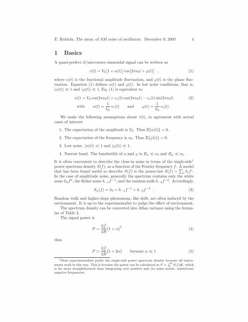
A quasi-perfect rf/microwave sinusoidal signal can be written as
v(t) = V0
[
1 + α(t)]
cos[
2πν0t + ϕ(t)]
, (1)
where α(t) is the fractional amplitude fluctuation, and ϕ(t) is the phase fluc-tuation. Equation (1) defines α(t) and ϕ(t). In low noise conditions, that is,|α(t)| ≪ 1 and |ϕ(t)| ≪ 1, Eq. (1) is equivalent to
We make the following assumptions about v(t), in agreement with actualcases of interest:
1. The expectation of the amplitude is V0. Thus Eα(t) = 0.
2. The expectation of the frequency is ν0. Thus Eϕ(t) = 0.
3. Low noise. |α(t)| ≪ 1 and |ϕ(t)| ≪ 1.
4. Narrow band. The bandwidth of α and ϕ is Bα ≪ ν0 and Bϕ ≪ ν0.
It is often convenient to describe the close-in noise in terms of the single-side1
power spectrum density S(f), as a function of the Fourier frequency f . A modelthat has been found useful to describe S(f) is the power-law S(f) =
∑
i hifi.
In the case of amplitiude noise, generally the spectrum contains only the whitenoise h0f
0, the flicker noise h−1f−1, and the random walk h−2f
−2. Accordingly,
Sα(f) = h0 + h−1f−1 + h−2f
−2 . (3)
Random walk and higher-slope phenomena, like drift, are often induced by theenvironment. It is up to the experimentalist to judge the effect of environment.
The spectrum density can be converted into Allan variance using the formu-lae of Table 2.
The signal power is
P =V 2
0
2R
(
1 + α)2
(4)
thus
P ≃ V 20
2R
(
1 + 2α)
because α ≪ 1 (5)
1Most experimentalists prefer the single-side power spectrum density because all instru-
ments work in this way. This is because the power can be calculated as P =∫
B
0S(f)df , which
is far more straightforward than integrating over positive and (to some extent, misterious)negative frequencies.
E. Rubiola, The meas. of AM noise of oscillators. December 9, 2005 5
Table 2: Relationships between power spectrum density and Allan variance.
noise type Spectrum density Sα(f) Allan variance σ2α(τ)
white h0
h0
2τ
flicker h−1f−1 h−1 2 ln(2)
random walk h−2f−2 h−2
4π2
6τ
It is convenient to rewrite P as P = P0 + δP , with
P0 =V 2
0
2Rand δP ≃ 2P0α (6)
The amplitude fluctuations are measured through the measurement of the powerfluctuation δP ,
α(t) =1
2
δP
P0
(7)
and of its power spectrum density,
Sα(f) =1
4S P
P0
(f) =1
4P 20
SP (f) . (8)
The measurement of a two-port device, like an amplifier, is made easy bythe availability of the reference signal sent to the device input. In this case, thebridge (interferometric) method [RG02] enables the measurement of amplitudenoise and phase noise with outstanding sensitivity. Yet, the bridge method cannot be exploited for the measurement of the AM noise of oscillators, synthesizersand other signal sources. Other methods are needed, based on power detectorsand on suitable signal processing techniques.
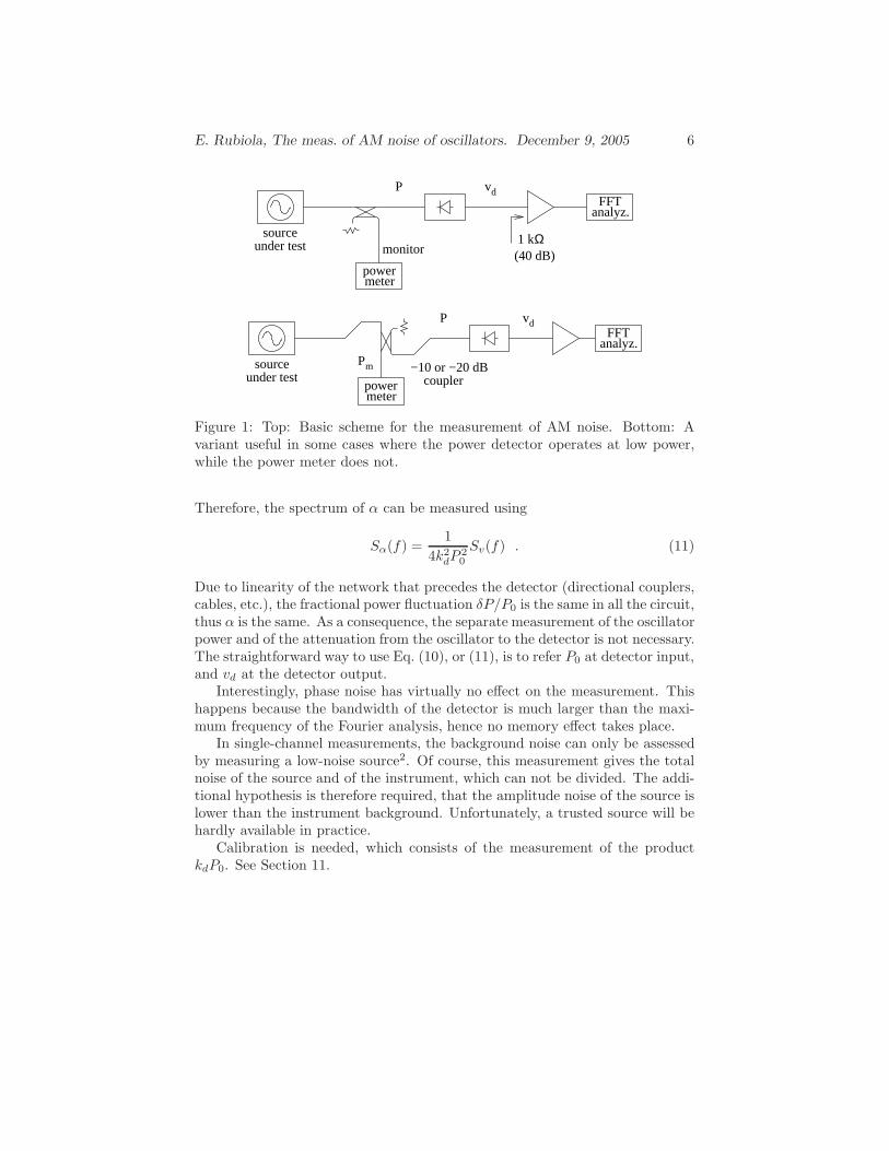
2 Single channel measurement
Figure 1 shows the basic scheme for the measurement of AM noise. The detectorcharacteristics (Sec. 4) is vd = kdP , hence the ac component of the detectedsignal is vd = kdδP . The detected voltage is related to α by vd = kdP0
δPP0
, thatis,
vd(t) = 2kdP0α(t) . (9)
Turning voltages into spectra, the above becomes
Sv(f) = 4k2dP
20 Sα(f) . (10)
E. Rubiola, The meas. of AM noise of oscillators. December 9, 2005 6
FFTanalyz.
powermeter
1 kΩsourceunder test
vd
(40 dB)
P
monitor
sourceunder test
powermeter
Pm
vdFFT
analyz.
P
−10 or −20 dBcoupler
Figure 1: Top: Basic scheme for the measurement of AM noise. Bottom: Avariant useful in some cases where the power detector operates at low power,while the power meter does not.
Therefore, the spectrum of α can be measured using
Sα(f) =1
4k2dP
20
Sv(f) . (11)
Due to linearity of the network that precedes the detector (directional couplers,cables, etc.), the fractional power fluctuation δP/P0 is the same in all the circuit,thus α is the same. As a consequence, the separate measurement of the oscillatorpower and of the attenuation from the oscillator to the detector is not necessary.The straightforward way to use Eq. (10), or (11), is to refer P0 at detector input,and vd at the detector output.
Interestingly, phase noise has virtually no effect on the measurement. Thishappens because the bandwidth of the detector is much larger than the maxi-mum frequency of the Fourier analysis, hence no memory effect takes place.
In single-channel measurements, the background noise can only be assessedby measuring a low-noise source2. Of course, this measurement gives the totalnoise of the source and of the instrument, which can not be divided. The addi-tional hypothesis is therefore required, that the amplitude noise of the source islower than the instrument background. Unfortunately, a trusted source will behardly available in practice.
Calibration is needed, which consists of the measurement of the productkdP0. See Section 11.
E. Rubiola, The meas. of AM noise of oscillators. December 9, 2005 7
monitor
sourceunder test
dual
cha
nnel
FF
T a
naly
zer
vb
va
Pb
Pa
powermeter
Figure 2: Correlation AM noise measurement.
meas. limit
α (f)
12m
f
log/log scale
cross spectrum
single channel
S
Figure 3: Spectra of the correlation AM noise measurement.
3 Dual channel (correlation) measurement
Figure 2 shows the scheme for the correlation measurement of AM noise. Thesignal is split into two branches, and measured by two separate power detectorsand amplifiers. Under the assumption that the two channels are independent,the cross spectrum Sba(f) is proportional to Sα(f). In fact, the two dc signalsare va = kaPaα and vb = kbPbα. The cross spectrum is
Sba(f) = 4kakbPaPbSα(f) , (12)
from which
Sα(f) =1
4kakbPaPb
Sba(f) . (13)
Averaging over m spectra, the noise of the individual channels is rejected bya factor
√2m (Fig. 3), for the sensitivity can be significantly increased. A
further advantage of the correlation method is that the measurement of Sα(f)is validated by the simultaneous measurement of the instrument noise limit,that is, the single-channel noise divided by
√2m. This solves one of the major
problems of the single-channel measurement, i.e., the need of a trusted low-noisesource.
2The reader familiar with phase noise measurements is used to measure the instrumentnoise by removing the device under test. This is not possible in the case of the AM noise ofthe oscillator.
E. Rubiola, The meas. of AM noise of oscillators. December 9, 2005 8
Ωk10050Ω toexternal
Ωk50Ω toexternal
100
video out rf inrf in
Ω~60
Ω~60
pF10−200pF
video out
10−200
Figure 4: Scheme of the diode power detector.
Larger is the power delivered by the source under test, larger is the in-strument gain. This applies to single-channel measurements, where the gain is4k2
dP20 [Eq. (10)], and to correlation measurements, where the gain is 4kakbPaPb
[Eq. (12)]. Yet in a correlation system the total power P0 is split into the twochannels, for PaPb = 1
4P 2
0 . Hence, switching from single-channel to correlationthe gain drops by a factor 1
4(−6 dB). Let us now compare a correlation system
to a single-channel system under the simplified hypothesis that the backgroundnoise referred at the detector output is unchanged. This happens if the noise ofthe dc preamplifier is dominant. In such cases, the background noise referredto the instrument input, thus to Sα, is multiplied by a factor 4√
2m. The nu-
merator “4” arises from the reduced gain, while the denominator√
2m is dueto averaging. Accordingly, it must be m > 8 for the correlation scheme to beadvantageous in terms of sensitivity. On the other hand, if the power of thesource under test is large enough for the system to work at full gain in bothcases, the dual-channel system exhibits higher sensitivity even at m = 1.
Calibration is about the same as for the single-channel measurements. SeeSection 11.
In laboratory practice, the availability of a dual-channel FFT analyzer is themost frequent critical point. If this instrument is available, the experimentalistwill prefer the correlation scheme in virtually all cases.
4 Schottky and tunnel diode power detectors
A rf/microwave power detector uses the nonlinear response of a diode to turnthe input power P into a dc voltage vd. The transfer function is
vd = kdP , (14)
which defines the detector gain kd. The physical dimension of kd is A−1. Thetechnical unit often used in data sheets is mV/mW, equivalent to A−1. Thediodes can only work at low input level. Beyond a threshold power, the outputvoltage differs smoothly from Eq. (14). The actual response depends on thediode type.
Figure 4 shows the scheme of actual power detectors. The input resistormatches the high input impedance of the diode network to the standard valueR0 = 50 Ω over the bandwidth and over the power range. The value depends on
E. Rubiola, The meas. of AM noise of oscillators. December 9, 2005 9
Table 3: some power-detector manufacturers (non-exhaustive list).
Table 4: Typical characteristics of Schottky and tunnel power detectors.
Schottky tunnel
input bandwidth up to 4 decades 1–3 octaves10MHz to 20GHz up to 40 GHz
vsvr max. 1.5:1 3.5:1max. input power (spec.) −15 dBm −15 dBmabsolute max. input power 20 dBm or more 20 dBmoutput resistance 1–10kΩ 50–200 Ωoutput capacitance 20–200 pF 10–50 pFgain 300 V/W 1000 V/Wcryogenic temperature no yes
the specific detector. The output capacitor filters the video3 signal, eliminatingcarrier from the output. A low capacitance makes the detector fast. On theother hand, a higher capacitance is needed if the detector is used to demodulatea low-frequency carrier. The two-diode configuration provides larger outputvoltage and some temperature compensation.
Power detectors are available off-the-shelf from numerous manufacturers,some of which are listed on Table 3. Agilent Technologies provides a series ofuseful application notes [Agi03] about the measurement of rf/microwave power.
Two types of diode are used in practice, Schottky and tunnel. Their typicalcharacteristics are shown in Table 4.
Schottky detectors are the most common ones. The relatively high outputresistance and capacitance makes the detector suitable to low-frequency carriers,starting from some 10 MHz (typical). In this condition the current flowing
3From the early time of electronics, the term ‘video’ is used (as opposed to ‘audio’) toemphasize the large bandwidth of the demodulated signal, regardless of the real purposes.
E. Rubiola, The meas. of AM noise of oscillators. December 9, 2005 10
1
2
5
10
20
50
100
200
500
100
−30 −20 −10 0 10
100Ω
1 kΩ
100 kΩou
tput
vol
tage
, mV
input power, dBm
Figure 5: Response of a two-diode power detector.
through the diode is small, and the input matching to R0 = 50 Ω is providedby a low value resistor. Thus, the VSWR is close to 1:1 in a wide frequencyrange. Most of the input power is dissipated in the input resistance, whichreduces the risk of damage in case of overload. A strong preference for negativeoutput voltage seems to derive from the lower noise of P type Schottky diodes,as compared to N type ones, in conjunction with practical issues of mechanicallayout. Figure 5 shows the response of a two-diode Schottky power detector.The quadratic response [Eq. (14)] derives from the diode resistance Rd, whichis related to the saturation current I0 by
Rd =ηVT
qI0
, (15)
where η ∈ [1 . . . 2] is a parameter that derives from the junction technology;VT = kT/q ≃ 25.6 mV at room temperature is the thermal voltage. At higherinput level, Rd becomes too small and the detector response turns smoothlyfrom quadratic to linear, like the response of the common AM demodulatorsand power rectifiers.
Tunnel detectors are actually backward detectors. The backward diode is atunnel diode in which the negative resistance in the forward-bias region is madenegligible by appropriate doping, and used in the reverse-bias region. Mostof the work on such detectors dates back to the sixties [Bur63, Gab67, Hal60].Tunnel detectors exhibit fast switching and higher gain than the Schottky coun-terpart. A low output resistance is necessary, which affects the input impedance.Input impedance matching is therefore poor. In the measurement of AM noise,as in other applications in which fast response is not relevant, the output re-sistance can be higher than the recommended value, and limited only by noiseconsiderations. At higher output resistance the gain further increases. Tunneldiodes also work in cryogenic environment, provided the package tolerates themechanical stress of the thermal contraction.
E. Rubiola, The meas. of AM noise of oscillators. December 9, 2005 11
0
-100
-30
-20
-50 -40
-80
-60
-60 100-10-20
-40
-120
Ω
320Ω
1 kΩ
3.2 kΩ
10 kΩ
input power, dBm
outp
ut v
olta
ge, d
BV
100
Herotek DZR124AA s.no. 227489
Figure 6: Measured response of a Schottky detector Herotek DZR124AA.
-50
-40
-20
-60
100-10-20-30-40-60
-80
-100
kΩ
3.2 kΩ
320Ω
100Ω
1 kΩ
input power, dBm
outp
ut v
olta
ge, d
BV
10
Herotek DT8012 s.no. 232028
Figure 7: Measured response of a tunnel detector Herotek DT8012.
E. Rubiola, The meas. of AM noise of oscillators. December 9, 2005 12
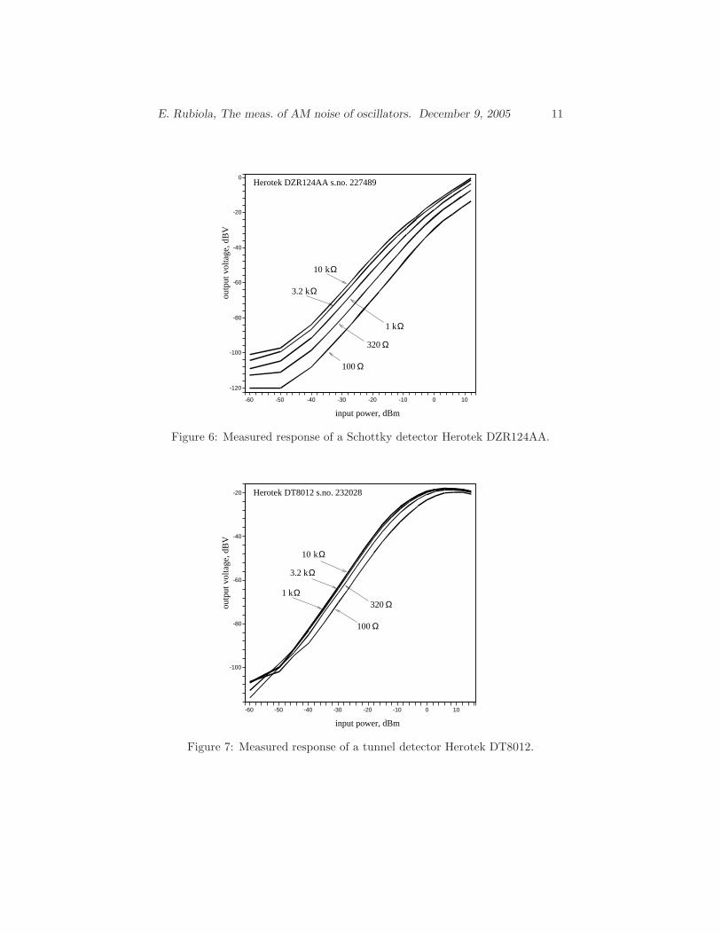
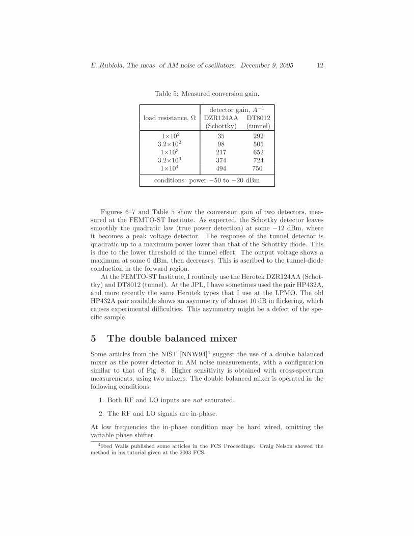
Figures 6–7 and Table 5 show the conversion gain of two detectors, mea-sured at the FEMTO-ST Institute. As expected, the Schottky detector leavessmoothly the quadratic law (true power detection) at some −12 dBm, whereit becomes a peak voltage detector. The response of the tunnel detector isquadratic up to a maximum power lower than that of the Schottky diode. Thisis due to the lower threshold of the tunnel effect. The output voltage shows amaximum at some 0 dBm, then decreases. This is ascribed to the tunnel-diodeconduction in the forward region.
At the FEMTO-ST Institute, I routinely use the Herotek DZR124AA (Schot-tky) and DT8012 (tunnel). At the JPL, I have sometimes used the pair HP432A,and more recently the same Herotek types that I use at the LPMO. The oldHP432A pair available shows an asymmetry of almost 10 dB in flickering, whichcauses experimental difficulties. This asymmetry might be a defect of the spe-cific sample.
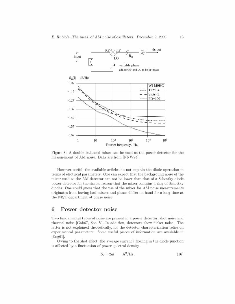
5 The double balanced mixer
Some articles from the NIST [NNW94]4 suggest the use of a double balancedmixer as the power detector in AM noise measurements, with a configurationsimilar to that of Fig. 8. Higher sensitivity is obtained with cross-spectrummeasurements, using two mixers. The double balanced mixer is operated in thefollowing conditions:
1. Both RF and LO inputs are not saturated.
2. The RF and LO signals are in-phase.
At low frequencies the in-phase condition may be hard wired, omitting thevariable phase shifter.
4Fred Walls published some articles in the FCS Proceedings. Craig Nelson showed themethod in his tutorial given at the 2003 FCS.
E. Rubiola, The meas. of AM noise of oscillators. December 9, 2005 13
LO
RF IF
R0
rfinput
variable phase
dc out
adj. for RF and LO to be in−phase
Fourier frequency, Hz
α−107
(f) dB/Hz
−117
−127
−137
−147
−157
−167
1 10 102 103 104 105
TFM−4WJ M9HC
SRA−1PD−100
S
Figure 8: A double balanced mixer can be used as the power detector for themeasurement of AM noise. Data are from [NNW94].
However useful, the available articles do not explain the diode operation interms of electrical parameters. One can expect that the background noise of themixer used as the AM detector can not be lower than that of a Schottky-diodepower detector for the simple reason that the mixer contains a ring of Schottkydiodes. One could guess that the use of the mixer for AM noise measurementsoriginates from having had mixers and phase shifter on hand for a long time atthe NIST department of phase noise.
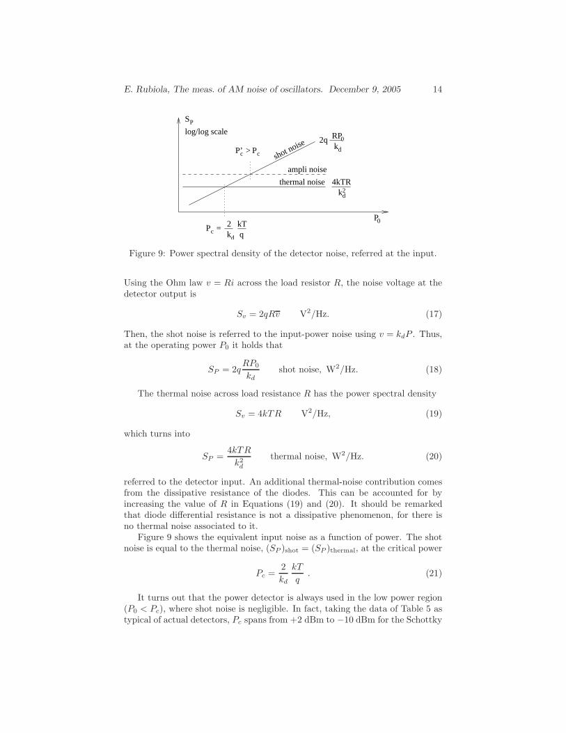
6 Power detector noise
Two fundamental types of noise are present in a power detector, shot noise andthermal noise [Gab67, Sec. V]. In addition, detectors show flicker noise. Thelatter is not explained theoretically, for the detector characterization relies onexperimental parameters. Some useful pieces of information are available in[Eng61].
Owing to the shot effect, the average current ı flowing in the diode junctionis affected by a fluctuation of power spectral density
Si = 2qı A2/Hz, (16)
E. Rubiola, The meas. of AM noise of oscillators. December 9, 2005 14
0
P
dk24kTR
kd
2q RP0
Pc kd
2 kTq
=
cP’ cP>
log/log scale
thermal noise
ampli noise
shot noise
P
S
Figure 9: Power spectral density of the detector noise, referred at the input.
Using the Ohm law v = Ri across the load resistor R, the noise voltage at thedetector output is
Sv = 2qRv V2/Hz. (17)
Then, the shot noise is referred to the input-power noise using v = kdP . Thus,at the operating power P0 it holds that
SP = 2qRP0
kd
shot noise, W2/Hz. (18)
The thermal noise across load resistance R has the power spectral density
Sv = 4kTR V2/Hz, (19)
which turns into
SP =4kTR
k2d
thermal noise, W2/Hz. (20)
referred to the detector input. An additional thermal-noise contribution comesfrom the dissipative resistance of the diodes. This can be accounted for byincreasing the value of R in Equations (19) and (20). It should be remarkedthat diode differential resistance is not a dissipative phenomenon, for there isno thermal noise associated to it.
Figure 9 shows the equivalent input noise as a function of power. The shotnoise is equal to the thermal noise, (SP )shot = (SP )thermal, at the critical power
Pc =2
kd
kT
q. (21)
It turns out that the power detector is always used in the low power region(P0 < Pc), where shot noise is negligible. In fact, taking the data of Table 5 astypical of actual detectors, Pc spans from +2 dBm to −10 dBm for the Schottky
E. Rubiola, The meas. of AM noise of oscillators. December 9, 2005 15
diodes (35 A−1 < kd < 500 A−1), and from −8 dBm to −12 dBm for the tunneldiodes (330 A−1 < kd < 820 A−1), depending on the load resistance. On theother hand, the detector turns from the quadratic (power) response to the linear(voltage) response at a significantly lower power. This can be seen on Figure 6and 7.
Looking at the specifications of commercial power detectors, informationabout noise is scarce. Some manufacturers give the NEP (Noise EquivalentPower) parameter, i.e., the power at the detector input that produces a videooutput equal to that of the device noise. In no case is said whether the NEPincreases or not in the presence of a strong input signal, which is related toprecision. Even worse, no data about flickering is found in the literature or inthe data sheets. Only one manufacturer (Herotek) claims the low flicker featureof its tunnel diodes, yet without providing any data.
The power detector is always connected to some kind of amplifier, whichis noisy. Denoting with (h0)ampli and (h−1)ampli the white and flicker noisecoefficients of the amplifier, the spectrum density referred at the input is
SP (f) =(h0)ampli
k2d
+(h−1)ampli
kdd
1
f. (22)
The amplifier noise coefficient (h0)ampli is connected to the noise figure by(h0)ampli = (F − 1)kT . Yet we prefer not to use the noise figure because ingeneral the amplifier noise results from voltage noise and current noise, whichdepends on R. Equation (22) is rewritten in terms of amplitude noise usingα = 1
2δPP0
[Eq. (7)]. Thus,
Sα(f) =1
2P0
qR
kd
+1
P 20
kTR
k2d
+1
4P 20
(h0)ampli
k2d
+1
4P 20
(h−1)ampli
k2d
1
f. (23)
After the first term of Eq. (22), the critical power becomes
P ′c =
2
kd
kT
q+
(h0)ampli
2qRkd
. (24)
This reinforces the conclusion that in actual conditions the shot noise is negli-gible.
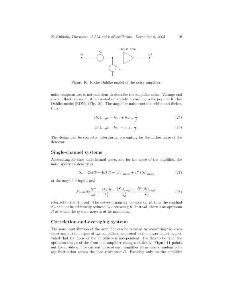
7 Design of the front-end amplifier
For optimum design, one should account for the detector noise and for thenoise of the amplifier, and find the most appropriate amplifier and operatingconditions. Yet, the optimum design relies upon the detailed knowledge of thepower-detector noise, which is one of our targets (Sec. 8). Thus, we provisionallyneglect the excess noise of the power detector. The first design is based on theavailable data, i.e., thermal noise and the noise of the amplifier. Operationalamplifiers or other types of impedance-mismatched amplifiers are often usedin practice. As a consequence, a single parameter, i.e., the noise figure or the
E. Rubiola, The meas. of AM noise of oscillators. December 9, 2005 16
invn
in
out
noise−free
Figure 10: Rothe-Dahlke model of the noisy amplifier.
noise temperature, is not sufficient to describe the amplifier noise. Voltage andcurrent fluctuations must be treated separately, according to the popular Rothe-Dahlke model [RD56] (Fig. 10). The amplifier noise contains white and flicker,thus
(Sv)ampli = h0,v + h−1,v
1
f(25)
(Si)ampli = h0,i + h−1,i
1
f. (26)
The design can be corrected afterwards, accounting for the flicker noise of thedetector.
Single-channel systems
Accounting for shot and thermal noise, and for the noise of the amplifier, thenoise spectrum density is
Sv = 2qRv + 4kTR + (Sv)ampli + R2 (Si)ampli (27)
at the amplifier input, and
SP = 2qRP
kd
+4kTR
k2d
+(Sv)ampli
k2d
+R2 (Si)ampli
k2d
(28)
referred to the rf input. The detector gain kd depends on R, thus the residualSP can not be arbitrarily reduced by decreasing R. Instead, there is an optimumR at which the system noise is at its minimum.
Correlation-and-averaging systems
The noise contribution of the amplifier can be reduced by measuring the crossspectrum at the output of two amplifiers connected to the power detector, pro-vided that the noise of the amplifiers is independent. For this to be true, theoptimum design of the front-end amplifier changes radically. Figure 11 pointsout the problem. The current noise of each amplifier turns into a random volt-age fluctuation across the load resistance R. Focusing only on the amplifier
E. Rubiola, The meas. of AM noise of oscillators. December 9, 2005 17
g
v1
i1
va
i2
v2 vb
rf in
R
g
Figure 11: The load resistor turns the current noise into fully-correlated noise.
noise, the voltage at the two outputs is
va = g (v1 + Ri1 + Ri2)
vb = g (v2 + Ri1 + Ri2)
The terms gv1 and gv2 are independent, for their contribution to the crossspectrum density is reduced by a factor 1√
2m, where m is the number of averaged
spectra. Conversely, a term
gR(i1 + i2)
is present at the two outputs. This term is exactly the same, thus it can not bereduced by correlation and averaging. Consequently, the lowest current noise isthe most important parameter, even if this is obtained at expense of a largervoltage noise. Yet, the rejection of larger voltage noise requires large m, forsome tradeoff may be necessary.
Examples
This section shows some design attempts, aimed at the lowest white and flickernoise at low Fourier frequencies, up to 0.1–1 MHz, where operational amplifierscan be exploited in a simple way.
A preliminary analysis reveals that, at the low resistance values required bythe detector, BJT amplifiers perform lower noise than field-effect transistors.On the other hand, the noise rejection by correlation and average requires lowcurrent noise, for JFET amplifiers are the best choice. In fact, BJTs can not beused because of the current noise, while MOSFETs show 1/f noise significantlylarger (10 dB or more) than JFETs.
Using two detectors (DZR124AA and DT8012), we try the operational am-plifiers and transistor pairs listed on Table 6. These amplifiers are selected withthe criterion that each one is a low-noise choice in its category.
AD743 and OPA627 are general-purpose precision JFET amplifiers, whichexhibit low bias current, hence low current noise. They are intended for
E. Rubiola, The meas. of AM noise of oscillators. December 9, 2005 18
Table 6: Noise parameters of some selected amplifiers.
voltage current
type white flicker white flicker notes
h0,v h−1,v h0,i h−1,i
AD743 2.9 18 6.9 − jfet op-amp
LT1028 0.9 1.7 1000 16 bjt op-amp
MAT02 0.9 1.6 900 1.6 npn bjt matched pair
MAT03 0.7 1.2 1200 11 pnp bjt matched pair
OP27 3.0 4.3 400 4.7 bjt op-amp
OP177 10 8.0 125 1.6 bjt op-amp
OP1177 8.0 8.3 200 1.5 bjt op-amp
OPA627 4.5 45 2.5 − jfet op-amp
unit nV√Hz
nV√Hz
fA√Hz
pA√Hz
correlation-and-averaging schemes (Fig. 11). The OP625 is similar tothe OP627 but for the frequency compensation, which enables unity-gainoperations, yet at expenses of speed. It is used successfully in the mea-surement of the excess noised of semiconductors, where large averagingsize is necessary in order to rid of the amplifier noise [SFF99].
LT1028 is a fast BJT amplifier with high bias current in the differential inputstage. This feature makes it suitable to low-noise applications in whichthe source resistance is low. In fact, the optimum noise resistance Rb =√
hv/hi is of 900 Ω for white noise, and of 105 Ω for flicker. These valuesare in the preferred range for proper operation of the power detectors.
MAT02 and MAT03 are bipolar matched pairs. They exhibit lower noisethan operational amplifiers, and they are suitable to the design for lowresistance of the source, like the LT1028. The MAT03 was successfullyemployed in the design of a low-noise amplifier optimized for 50 Ω sources[RLV04].
OP27 and OP37 are popular general-purpose precision BJT amplifiers, mostoften used in low-noise applications. Their noise characteristics are aboutidentical. The OP27 is fully compensated, for it is stable at closed-loopgain of one. The OP37 is only partially compensated, which requires aminimum closed-loop gain of five for stable operation. Of course, lowercompensation increases bandwidth and speed.
OP177 and OP1177 are general-purpose precision BJT amplifiers with lowbias current in the differential input stage, thus they exhibit lower currentnoise than other BJT amplifiers. They can be an alternative if the designbased on JFET amplifier fails.
E. Rubiola, The meas. of AM noise of oscillators. December 9, 2005 19
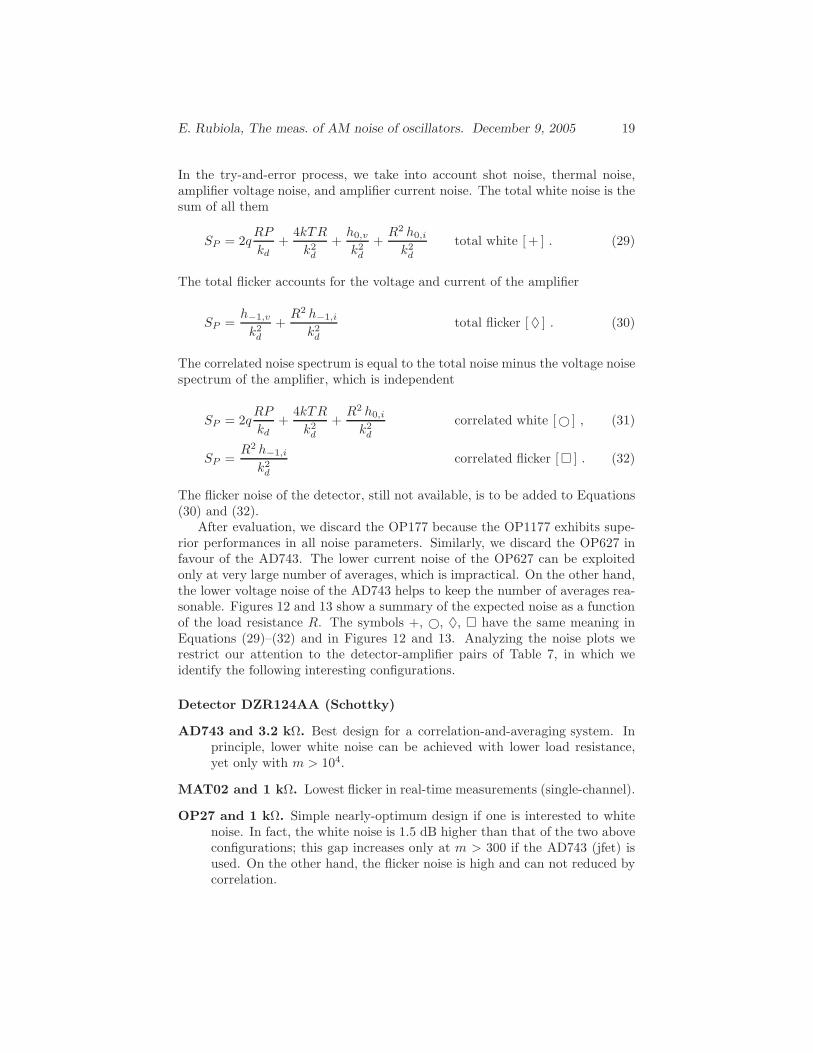
In the try-and-error process, we take into account shot noise, thermal noise,amplifier voltage noise, and amplifier current noise. The total white noise is thesum of all them
SP = 2qRP
kd
+4kTR
k2d
+h0,v
k2d
+R2 h0,i
k2d
total white [ + ] . (29)
The total flicker accounts for the voltage and current of the amplifier
SP =h−1,v
k2d
+R2 h−1,i
k2d
total flicker [ ♦ ] . (30)
The correlated noise spectrum is equal to the total noise minus the voltage noisespectrum of the amplifier, which is independent
AD743 and 3.2 kΩ. Best design for a correlation-and-averaging system. Inprinciple, lower white noise can be achieved with lower load resistance,yet only with m > 104.
MAT02 and 1 kΩ. Lowest flicker in real-time measurements (single-channel).
OP27 and 1 kΩ. Simple nearly-optimum design if one is interested to whitenoise. In fact, the white noise is 1.5 dB higher than that of the two aboveconfigurations; this gap increases only at m > 300 if the AD743 (jfet) isused. On the other hand, the flicker noise is high and can not reduced bycorrelation.
E. Rubiola, The meas. of AM noise of oscillators. December 9, 2005 20
White and shot noise, plus white and flicker noise of the amplifier.The flicker noise of the power detector is not accounted for.
Detector DT8012 (tunnel)
AD743 and 1 kΩ. Best design for a correlation-and-averaging system. Slightlylower white noise can be obtained at lower R, yet at expenses of larger mand of larger flicker noise.
LT1028 and 100 Ω. Simple nearly-optimum design for real-time (single chan-nel) systems. This configuration, as compared to the best one (MAT02with 320 Ω load) shows white noise 1.2 dB higher, and flicker noise 9 dBhigher.
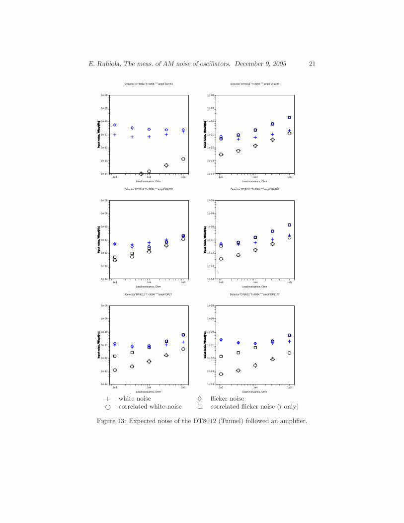
E. Rubiola, The meas. of AM noise of oscillators. December 9, 2005 23
MAT02 and 320 Ω. Lowest white and flicker noise in real-time measurements(single-channel).
MAT02 and 100 Ω. Close to the lowest white and flicker noise in real-timemeasurements (single-channel). Fairly good for correlation at moderateaveraging, up to m = 360 for white noise, and m = 90 for flicker.
Remark. Generally, tunnel detectors show higher gain than Schottky detec-tors. The fact that they exhibit lower noise is a consequence. On the otherhand, the Schottky detectors are often preferred because of wider bandwidth,and because of higher tolerance to electrical stress and to experimental errors.
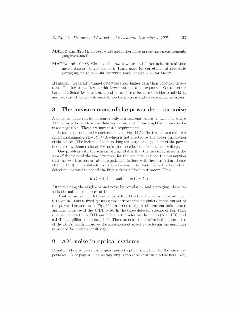
8 The measurement of the power detector noise
A detector alone can be measured only if a reference source is available whoseAM noise is lower than the detector noise, and if the amplifier noise can bemade negligible. These are unrealistic requirements.
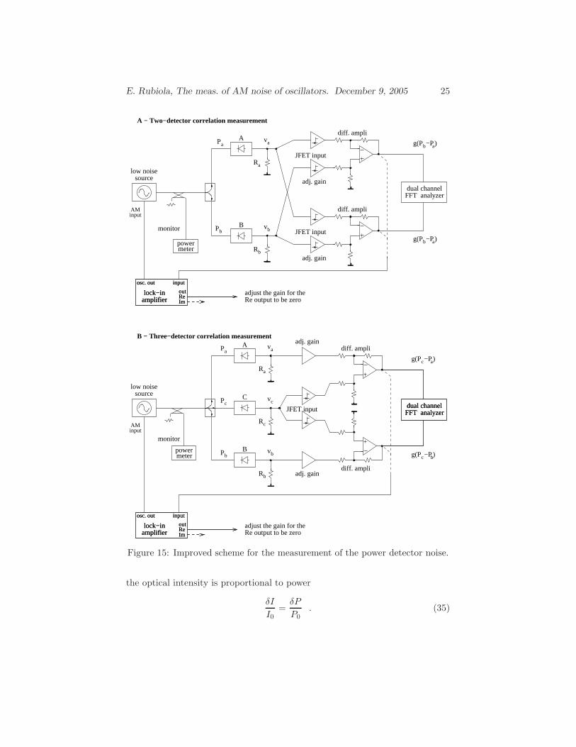
It useful to compare two detectors, as in Fig. 14A. The trick is to measure adifferential signal g(Pb −Pa) ≈ 0, which is not affected by the power fluctuationof the source. The lock-in helps in making the output independent of the powerfluctuations. Some residual PM noise has no effect on the detected voltage.
One problem with the scheme of Fig. 14A is that the measured noise is thesum of the noise of the two detectors, for the result relies upon the assumptionthat the two detectors are about equal. This is fixed with the correlation schemeof Fig. 14B). The detector c is the device under test, while the two otherdetectors are used to cancel the fluctuations of the input power. Thus
g(Pc − Pa) and g(Pc − Pb)
After rejecting the single-channel noise by correlation and averaging, there re-sults the noise of the detector C.
Another problem with the schemes of Fig. 14 is that the noise of the amplifieris taken in. This is fixed by using two independent amplifiers at the output ofthe power detector, as in Fig. 15. In order to reject the current noise, theseamplifier must be of the JFET type. In the three detector scheme of Fig. 14B,it is convenient to use BJT amplifiers in the reference branches (A and B), anda JFET amplifier in the branch C. The reason for this choice is the lower noiseof the BJTs, which improves the measurement speed by reducing the minimumm needed for a given sensitivity.
9 AM noise in optical systems
Equation (1) also describes a quasi-perfect optical signal, under the same hy-potheses 1–4 of page 4. The voltage v(t) is replaced with the electric field. Yet,
E. Rubiola, The meas. of AM noise of oscillators. December 9, 2005 24
B
powermeter
Pa
Pb
vb
va
FFTanalyz.
g(Pb−Pa)
sourcelow noise
input
lock−inamplifier Im
Reout
osc. out input
lock−inamplifier Im
Reout
osc. out
Pa
Pc
Pb vb
vc
va
powermeter
monitor
sourcelow noise
dual channelFFT analyzer
input
lock−inamplifier Im
Reout
osc. out input
lock−inamplifier Im
Reout
osc. out
g(Pc−Pa)
g(Pc−Pb)
diff. ampli
adj. gain
adj. gain
Re output to be zeroadjust the gain for the
A
B
C
B − Three−detector correlation measurement
monitor
diff. ampli
adj. gain
A − Differential measurement
AMinput
Re output to be zeroadjust the gain for the
A
Figure 14: Measurement of the power detector noise.
the preferred physical quantity used to describe the AM noise is the RelativeIntensity Noise (RIN), defined as
RIN = S δI
I0
(f) , (33)
that is, the power spectrum density of the normalized intensity fluctuation
(δI)(t)
I0
=I(t) − I0
I0
. (34)
The RIN includes both fluctuation of power and the fluctuation of the powercross-section distribution. If the cross-section distribution is constant in time,
E. Rubiola, The meas. of AM noise of oscillators. December 9, 2005 25
B − Three−detector correlation measurement
Pb
Pava
Ra
vb
Rb
dual channelFFT analyzer
g(Pb−Pa)
g(Pb−Pa)powermeter
AMinput
sourcelow noise
input
lock−inamplifier Im
Reout
osc. out input
lock−inamplifier Im
Reout
osc. out
Re output to be zeroadjust the gain for the
diff. ampli
diff. ampli
Pc
Rc
Pava
Ra
Pbvb
Rb
diff. ampli
dual channelFFT analyzer
g(Pc−Pa)
g(Pc−Pb)
dual channelFFT analyzer
diff. ampli
powermeter
sourcelow noise
input
lock−inamplifier Im
Reout
osc. out input
lock−inamplifier Im
Reout
osc. out
Re output to be zeroadjust the gain for the
AMinput
vc
adj. gain
adj. gain
monitor JFET input
JFET input
A
B
monitor
adj. gain
adj. gain
JFET input
A
C
B
A − Two−detector correlation measurement
Figure 15: Improved scheme for the measurement of the power detector noise.
the optical intensity is proportional to power
δI
I0
=δP
P0
. (35)
E. Rubiola, The meas. of AM noise of oscillators. December 9, 2005 26
monitor
FFTanalyz.
vd
coupler
powermeter
sourceundertest
powermeter
couplercoupler
sourceundertest
Pb
Pa
R
R
R
dual
cha
nnel
FF
T a
naly
zerva
vb
monitor
P
monitor
optical
optical dc
dc
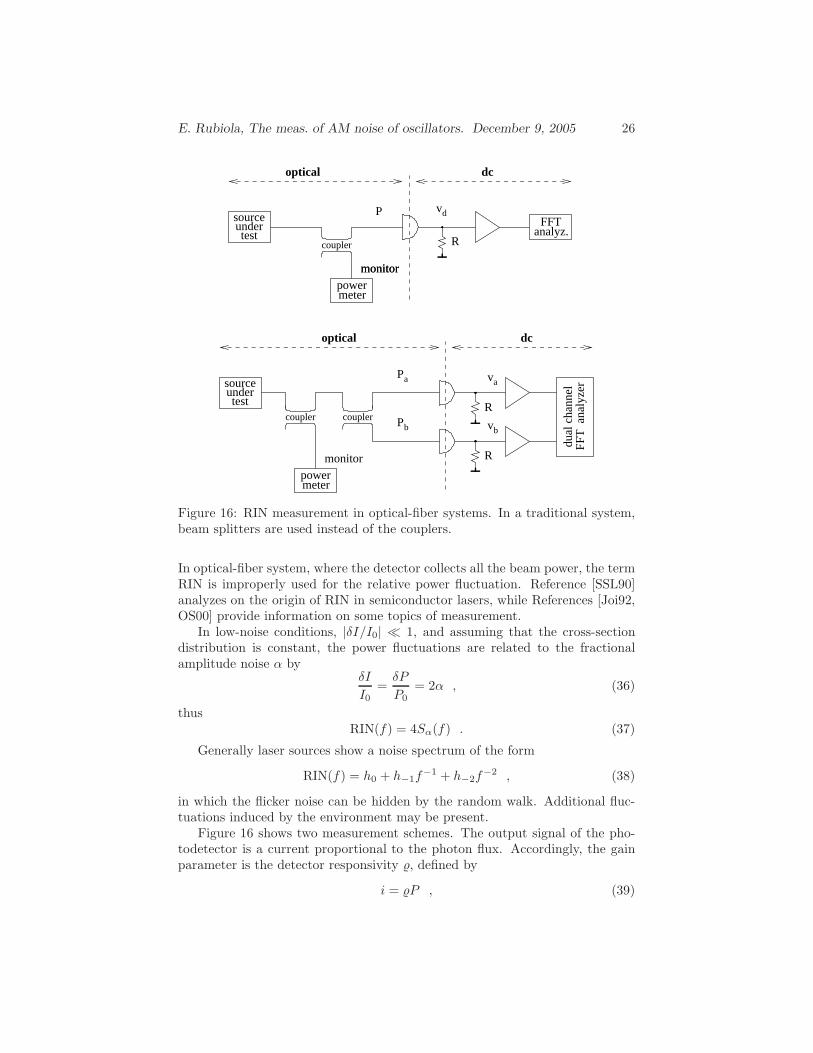
Figure 16: RIN measurement in optical-fiber systems. In a traditional system,beam splitters are used instead of the couplers.
In optical-fiber system, where the detector collects all the beam power, the termRIN is improperly used for the relative power fluctuation. Reference [SSL90]analyzes on the origin of RIN in semiconductor lasers, while References [Joi92,OS00] provide information on some topics of measurement.
In low-noise conditions, |δI/I0| ≪ 1, and assuming that the cross-sectiondistribution is constant, the power fluctuations are related to the fractionalamplitude noise α by
δI
I0
=δP
P0
= 2α , (36)
thusRIN(f) = 4Sα(f) . (37)
Generally laser sources show a noise spectrum of the form
RIN(f) = h0 + h−1f−1 + h−2f
−2 , (38)
in which the flicker noise can be hidden by the random walk. Additional fluc-tuations induced by the environment may be present.
Figure 16 shows two measurement schemes. The output signal of the pho-todetector is a current proportional to the photon flux. Accordingly, the gainparameter is the detector responsivity , defined by
i = P , (39)
E. Rubiola, The meas. of AM noise of oscillators. December 9, 2005 27
where
i =qηP
hν(40)
is the photocurrent, thus
=qη
hν. (41)
The schemes of Fig. 16 are similar to Fig. 1 (single-channel) and Fig. 2(cross-spectrum). The dual-channel scheme is preferred because of the highersensitivity, and because it makes possible to validate the measurement throughthe number of averaged spectra.
Noise is easily analyzed with the methods shown in Section 7. Yet in thiscase the virtual-ground amplifier is often preferred, which differs slightly fromthe examples shown in Section 7. A book [Gra96] is entirely devoted to thespecial case of the photodiode amplifier.
10 AM noise in microwave photonic systems
Microwave and rf photonics is being progressively recognized as an emergingdomain of technology [Cha02, SJMN06]. It is therefore natural to investigate innoise in these systems.
The power5 Pλ(t) of the optical signal is sinusoidally modulated in intensityat the microwave frequency νµ is
Pλ(t) = Pλ (1 + m cos 2πνµt) , (42)
where m is the modulation index6. Eq. (42) is similar to the traditional AMof radio broadcasting, but optical power is modulated instead of RF voltage.In the presence of a distorted (nonlinear) modulation, we take the fundamentalmicrowave frequency ν0. The detector photocurrent is
i(t) =qη
hνλ
Pλ (1 + m cos 2πνµt) , (43)
where η the quantum efficiency of the photodetector. The oscillation termm cos 2πνµt of Eq. (43) contributes to the microwave signal, the term “1” doesnot. The microwave power fed into the load resistance R0 is Pµ = R0ı2, hence
Pµ =1
2m2R0
(
qη
hνλ
Pλ
)2
. (44)
The discrete nature of photons leads to the shot noise of power spectraldensity 2qiR [W/Hz] at the detector output. By virtue of Eq. (43),
Ns = 2q2η
hνλ
PλR (shot noise) . (45)
5In this section we use the subscript λ for ‘light’ and µ for ‘microwave’.6We use the symbol m for the modulation index, as in the general literature. There is no
ambiguity because the number of averages (m) is not used in this section.
E. Rubiola, The meas. of AM noise of oscillators. December 9, 2005 28
monitor
R0
R0
Pa
Pb
coupler
powermeter
coupler
sourceundertest
R
R
va
vb
dual
cha
nnel
FF
T a
naly
zer
powermeter
microwaveoptical
monitor
dc
Figure 17: Measurement of the microwave AM noise of a modulated light beam.
In addition, there is the equivalent input noise of the amplifier loaded by R,whose power spectrum is
Nt = FkT (thermal noise and amplifier noise) , (46)
where F is the noise figure of the amplifier, if any, at the output of the pho-todetector. The white noise Ns + Nt turns into a noise floor
Sα =Ns + Nt
Pµ
. (47)
Using (44), (45) and (46), the floor is
Sα =2
m2
[
2hνλ
η
1
Pλ
+FkT
R
(
hνλ
qη
)2 (
1
Pλ
)2]
. (48)
Interestingly, the noise floor is proportional to (Pλ)−2 at low power, and to(Pλ)−1 above the threshold power
Pλ,t =1
2
FkT
R
hνλ
q2η(49)
For example, taking νλ = 193.4 THz (wavelength λ = 1.55 µm), η = 0.6, F = 1(noise-free amplifier), and m = 1, we get a threshold power Pλ,t = 335 µW,which sets the noise floor at 5.1×10⁻¹⁵ Hz−1 (−143 dB/Hz).
Figure 17 shows the scheme of a correlation system for the measurement ofthe microwave AM noise. It may be necessary to add a microwave amplifier atthe output of each photodetector. Eq. (48) holds for one arm of Fig. 17. Asthere are two independent arms, the noise power is multiplied by two.
Finally, it is to be pointed out that the results of this section concern only thewhite noise of the photodetector and of the microwave amplifier at the photode-tector output. Experimental method and some data in the close-in microwave
E. Rubiola, The meas. of AM noise of oscillators. December 9, 2005 29
flickering of the high-speed photodetectors is available in Reference [RSYM06].The noise of the microwave power detector and of its amplifier is still to beadded, according to Section 6.
11 Calibration
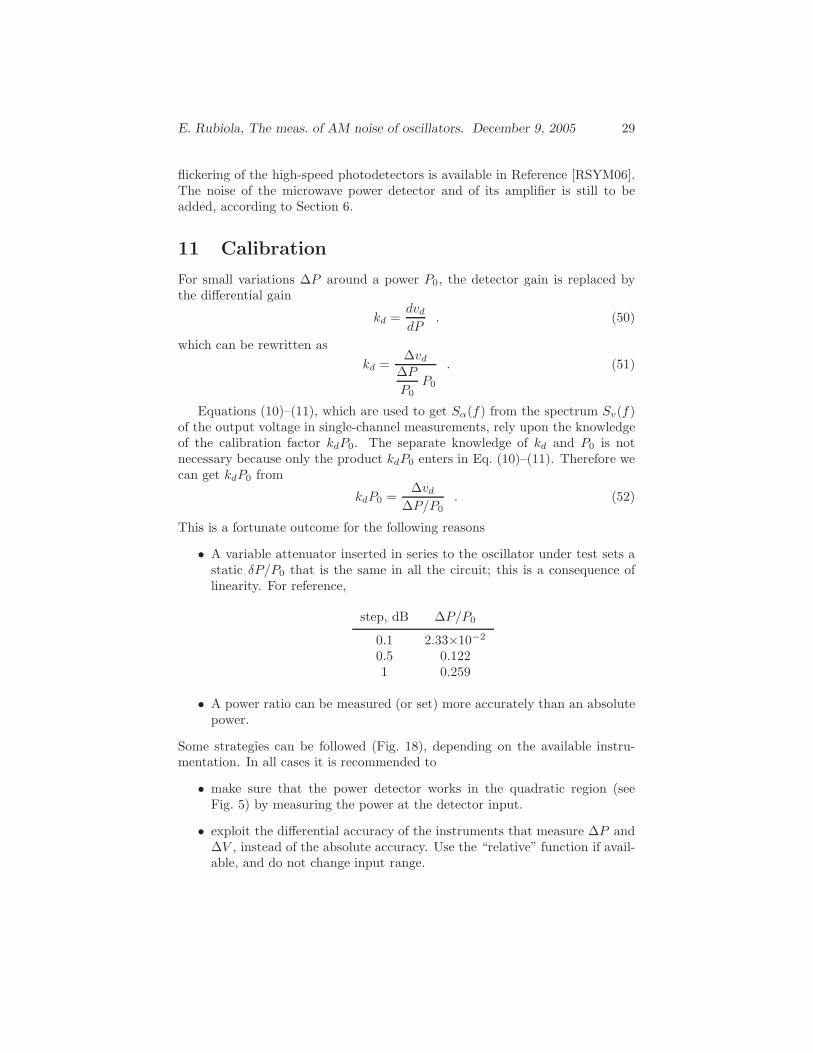
For small variations ∆P around a power P0, the detector gain is replaced bythe differential gain
kd =dvd
dP. (50)
which can be rewritten as
kd =∆vd
∆P
P0
P0
. (51)
Equations (10)–(11), which are used to get Sα(f) from the spectrum Sv(f)of the output voltage in single-channel measurements, rely upon the knowledgeof the calibration factor kdP0. The separate knowledge of kd and P0 is notnecessary because only the product kdP0 enters in Eq. (10)–(11). Therefore wecan get kdP0 from
kdP0 =∆vd
∆P/P0
. (52)
This is a fortunate outcome for the following reasons
• A variable attenuator inserted in series to the oscillator under test sets astatic δP/P0 that is the same in all the circuit; this is a consequence oflinearity. For reference,
step, dB ∆P/P0
0.1 2.33×10⁻²
0.5 0.1221 0.259
• A power ratio can be measured (or set) more accurately than an absolutepower.
Some strategies can be followed (Fig. 18), depending on the available instru-mentation. In all cases it is recommended to
• make sure that the power detector works in the quadratic region (seeFig. 5) by measuring the power at the detector input.
• exploit the differential accuracy of the instruments that measure ∆P and∆V , instead of the absolute accuracy. Use the “relative” function if avail-able, and do not change input range.
E. Rubiola, The meas. of AM noise of oscillators. December 9, 2005 30
attenuator
voltm.
powermeter
sourceunder test
atten
0.1 dB step
sourceunder test
atten
0.1 dBstep
powermeter
Pb
Pa va
vb
voltm.
voltm.
synthes.
powermeter
Pm
Pm
vd
vd
P
B − By−step attenuator
C − Correlation system
A − Synthesizer
P
internalvariable
Figure 18: Calibration schemes.
• avoid plugging and unplugging connectors during the measurement. Adirectional coupler is needed not to disconnect the power detector for themeasurement of ∆P .
In Fig. 18A, the internal variable attenuator of a synthesizer is used to mea-sure kdP0. ∆P/P0 can be measured with the power meter, or obtained fromthe calibration of the synthesizer internal attenuator. Some modern synthesiz-ers have a precise attenuator that exhibit a resolution of 0.1 or 0.01 dB. InFig. 18B, a calibrated by-step attenuator is inserted between the source undertest and the power detector. By-step attenuators can be accurate up to some3–5 GHz. Beyond, one can use a multi-turn continuous attenuator and rely onthe power meter. In the case of correlation measurements (Fig. 18C), symmetryis exploited to measure ka and kb in a condition as close as possible to the finalmeasurement of Sα(f). Of course, it holds that ∆Pa/Pa = ∆Pb/Pb.
E. Rubiola, The meas. of AM noise of oscillators. December 9, 2005 31
B − Improved AC calibration
0
sourceunder test
sourceunder test
reference
νs
reference
atten
atten
ν0
νs
atten
atten
νb ν0 νs= | − |
input
amplifier ImReoutlock−in
ref in
powermeter
Pb
Pa va
vb
voltm.
powermeter
Pb
Pa va
vb
voltm.
narrow−bandac voltmeter
or FFT analyzer
νb ν0 νs= | − |
B − AC calibration
ν
Figure 19: Alternate calibration schemes.
11.1 Alternate calibration method
Another method to calibrate the power detector makes use of two synthesizersin the frequency region of interest, so that the beat note falls in the audiofrequencies (Fig. 19). This scheme is inspired to the two-tone method, chieflyused to measure the deviation of the detector from the ideal law vd = kdP[RST+95, WCS04].
Using P = v2
R, and denoting the carrier and the reference sideband with
v0(t) = V0 cos(2πν0t) and vs(t) = Vs cos(2πνst), respectively, the detected signal
E. Rubiola, The meas. of AM noise of oscillators. December 9, 2005 32
is
vd(t) =kd
R
v0(t) + vs(t)2
∗ hlp(t) . (53)
The low-pass function hlp keeps the dc and the beat note at the frequencyνb = νs − ν0, and eliminates the νs + ν0 terms. Thus,
vd(t) =kd
R
1
2V 2
0 +1
2V 2
s + 21
2V0Vs cos
[
2π(νs − ν0)t]
, (54)
which is split into the dc term
vd = kd
V 20 + V 2
s
2R(55)
and the beat-note term
vd(t) = 2kd
R
V0Vs
2cos
[
2π(νs − ν0)t]
, (56)
hence
(
Vd
)
rms= kd
√
2P0Ps . (57)
The dc term [Eq. (55)] makes it possible to measure kd from the contrastbetween v1, observed with the carrier alone, and v2, observed with both signals.Thus,
kd =v2 − v1
Ps
(58)
Alternatively, the ac term [Eq. (57)] yields
kd =
(
Vd
)
rms√2P0Ps
(59)
The latter is appealing because the assessment of kd relies only on ac mea-surements, which are free from offset and thermal drift. On the other hand,the two-tone measurement does not provide the straight measurement of theproduct kdP0.
12 Examples
Figure 20 show an example of AM noise measurement. The source under testis a 100 MHz quartz oscillator (Wenzel 501-04623E serial no. 3752-0214).
Calibration is done by changing the power P0 = −10.2 dBm by ±0.1 dB.There results ka = 1.28×10⁵ V/W and kb = 1.34×10⁵ V/W, including the 52dB amplifier (321 V/W and 336 V/W without amplification). The system gainis therefore 4kakbPaPb = 641 V2 (28.1 dBV2).
E. Rubiola, The meas. of AM noise of oscillators. December 9, 2005 33
−10.2dBm
Ωk10
Ωk10
madehome
dual
cha
nnel
FF
T a
naly
zer
3052AHP+13dBm −6.9dBm
atten
0.1 dB step
3055Weinschel
atten
B=2MHz100MHz
madehome
Wenzel501−04623E
under test
100MHzOCXO
MacomT−1000
DZR 124AAHerotek
52dB
Wenzel 501-04623E (s/n 3572-0214)
Pd = 9.5 µW (−10.2 dBm)kd = 1.31×10⁵ A−1 with dc amplim = 638 averaged spectra
1/√
2m = 35.7 (15.5 dB)
h−1 = 1.15×10⁻¹² Hz−1 (−129.4 dB)
σα = 4×10⁻⁷
Figure 20: Example of AM noise measurement.
The cross spectrum of Fig. 20 is Sba = 1.26×10⁻¹¹ V2 (−109 dBV2/Hz)at 10 Hz, of the flicker type. Averaging over m = 638 spectra, the single-channel noise is rejected by
√2×638 = 35.7 (15.5 dB). The displayed flicker
(−109 dB at 10 Hz) exceeds by only 3.8 dB the rejected single-channel noise.A correction of a factor 0.58 (−2.3 dB) is therefore necessary. The correctedflicker is Sba = 7.4×10⁻¹¹ V2 (−101.3 dBV2/Hz) extrapolated at 1 Hz. Thewhite noise can not be obtained from Fig. 20 because of the insufficient numberof averaged spectra.
As a consequence of the low amplitude noise of the oscillator, it is possibleto measure the noise of single channel, which includes detector and amplifier.Accounting for the gain (28.1 dBV2), the single-channel flicker noise of Fig. 20at 1 Hz is Sα(1 Hz) = 2.5×10⁻¹² Hz−1 (−116.1 dB/Hz) for one channel, and
E. Rubiola, The meas. of AM noise of oscillators. December 9, 2005 34
Table 8: AM noise of some sources.
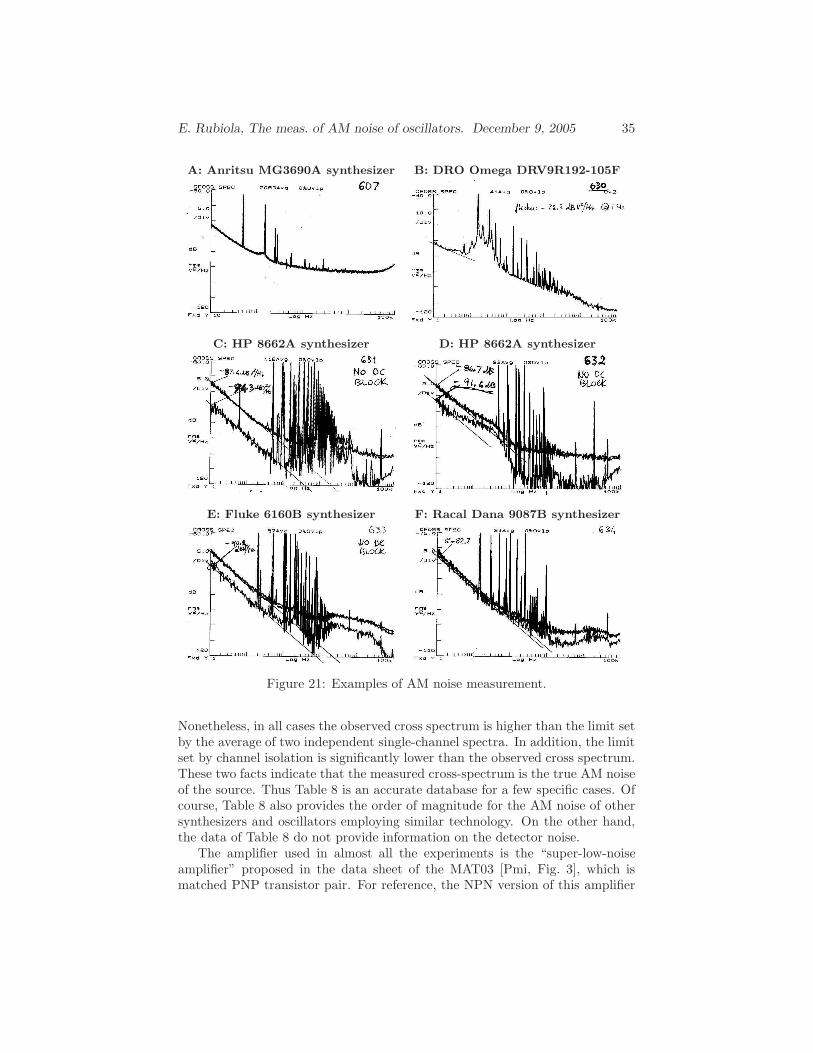
source h−1 σα notes
Anritsu MG3690A 2.5×10⁻¹¹ 5.9×10⁻⁶ Fig. 21Asynthesizer (10 GHz) −106.0 dB
Omega DRV9R192-105F 8.1×10⁻¹¹ 1.1×10⁻⁶ Fig. 21B9.2 GHz DRO −100.9 dB bump and junks
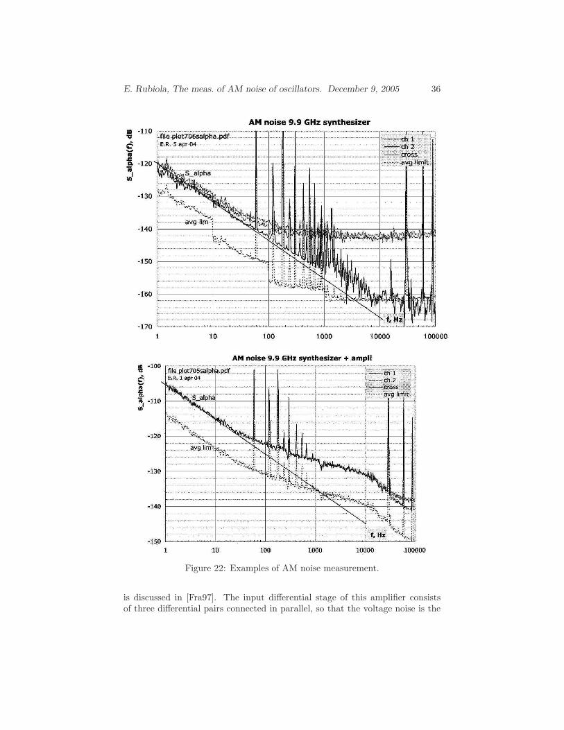
Narda DBP-0812N733 2.9×10⁻¹¹ 6.3×10⁻⁶ Fig. 22A/Bamplifier (9.9 GHz) −105.4 dB
HP 8662A no. 1 6.8×10⁻¹³ 9.7×10⁻⁷ Fig. 21Csynthesizer (100 MHz) −121.7 dB junks
HP 8662A no. 2 1.3×10⁻¹² 1.4×10⁻⁶ Fig. 21Dsynthesizer (100 MHz) −118.8 dB junks
Fluke 6160B 1.5×10⁻¹² 1.5×10⁻⁶ Fig. 21Esynthesizer −118.3 dB junks
Racal Dana 9087B 8.4×10⁻¹² 3.4×10⁻⁶ Fig. 21Fsynthesizer (100 MHz) −110.8 dB junks
Wenzel 500-02789D 4.7×10⁻¹² 2.6×10⁻⁶ Fig. 20100 MHz OCXO −113.3 dB
Wenzel 501-04623E no. 1 2.0×10⁻¹³ 5.2×10⁻⁷
100 MHz OCXO −127.1 dB
Wenzel 501-04623E no. 2 1.3×10⁻¹³ 4.3×10⁻⁷
100 MHz OCXO −128.8 dB
Sα(1 Hz) = 3.4×10⁻¹² Hz−1 (−114.7 dB/Hz) for the other channel.The AM flickering of the oscillator is Sα(1 Hz) = 1.15×10⁻¹³ Hz−1 (−129.4
dB/Hz), thus h−1 = 1.14×10⁻¹³. Using the conversion formula of Tab. 2 forflicker noise, the Allan variance is σ2
α = 1.6×10⁻¹³, which indicates an amplitudestability σα = 4×10⁻⁷, independent of the measurement time τ .
Table 8 shows some examples of AM noise measurement. The measuredspectra are in Fig. 20, 21, and 22
All the experiments of Tab. 8 and Fig. 20, 21, and 22 were done before think-ing seriously about the design of the front-end amplifier (Section 7), and beforemeasuring the detector gain as a function of the load resistance (Table 5, andFigures 6–7). The available low-noise amplifiers, designed for other purposes,turned out to be a bad choice, far from being optimized for this application.
E. Rubiola, The meas. of AM noise of oscillators. December 9, 2005 35
E: Fluke 6160B synthesizer F: Racal Dana 9087B synthesizer
Figure 21: Examples of AM noise measurement.
Nonetheless, in all cases the observed cross spectrum is higher than the limit setby the average of two independent single-channel spectra. In addition, the limitset by channel isolation is significantly lower than the observed cross spectrum.These two facts indicate that the measured cross-spectrum is the true AM noiseof the source. Thus Table 8 is an accurate database for a few specific cases. Ofcourse, Table 8 also provides the order of magnitude for the AM noise of othersynthesizers and oscillators employing similar technology. On the other hand,the data of Table 8 do not provide information on the detector noise.
The amplifier used in almost all the experiments is the “super-low-noiseamplifier” proposed in the data sheet of the MAT03 [Pmi, Fig. 3], which ismatched PNP transistor pair. For reference, the NPN version of this amplifier
E. Rubiola, The meas. of AM noise of oscillators. December 9, 2005 36
Figure 22: Examples of AM noise measurement.
is discussed in [Fra97]. The input differential stage of this amplifier consistsof three differential pairs connected in parallel, so that the voltage noise is the
E. Rubiola, The meas. of AM noise of oscillators. December 9, 2005 37
noise of a pair divided by√
3. Yet the current noise is multiplied by√
3. As aconsequence, the amplifier is noise-matched to an impedance of some 200 Ω forflicker noise, and to some 30 Ω for white noise, which is too low for our purposes.The second version of the MAT03 amplifier, designed after the described exper-iments, was optimized for the lowest flicker when connected to a 50 Ω source[RLV04]. This amplifier, now routinely employed for the measurement of phasenoise, makes use one MAT03 instead of three. In two cases (Fig. 22) a differentamplifier was used, based on the OP37 operational amplifier loaded to an inputresistance of some 1 kΩ. Interestingly, in the operating conditions of AM noisemeasurements, the OP37 outperforms the more sophisticated MAT03.
13 Final remarks
True quadratic detection vs. peak detection. Beyond a threshold power,a power detector leaves the quadratic operations and works as a peak detector.The peak detection is the same operation mode of the old good detectors forAM broadcasting (which is actually an envelope modulation). This operationmode exhibits higher gain, hence it could be advantageous for the measurementof low-noise signals. The answer may depend on the diode type, Schottky ortunnel. The strong recommendation to use the diode in the quadratic regionmight be wrong.
Trans-resistance amplifiers. In principle, the power detector can be used asa power-to-current converter (instead of as a power-to-voltage) converter, andconnected to a trans-resistance amplifier. The advantage is that the resistorat the detector output, which is a relevant source of noise in voltage-modemeasurements, is not present. This choice, suggested in [Bur63], is never foundin the technical literature accompanying the detectors.
Cryogenic environment. In principle, the tunnel diode should work at cryo-genic temperatures. Yet, the laboratory could be much less smooth than thetheory.
References
[Agi03] Agilent Technologies, Inc., Paloalto, CA, Fundamentals of RF andmicrowave power measurements, Part 1–4, 2003. 4
[Bur63] C. A. Burrus, Backward diodes for low-level millimeter-wave detec-tion, IEEE Trans. Microw. Theory Tech. 11 (1963), no. 9, 357–362.4, 13
[Cha02] William S. C. Chang (ed.), RF photonic technology in optical fiberlinks, Cambridge, Cambridge, UK, 2002. 10
E. Rubiola, The meas. of AM noise of oscillators. December 9, 2005 38
[Eng61] Sverre T. Eng, Low-noise properties of microwave backward diodes,IRE Trans. Microw. Theory Tech. 9 (1961), no. 5, 419–425. 6
[Fra97] Sergio Franco, Design with operational amplifiers and analog inte-grated circuits, 2nd ed., McGraw Hill, Singapore, 1997. 12
[Gab67] William F. Gabriel, Tunnel-diode low-level detection, IEEE Trans.Microw. Theory Tech. 15 (1967), no. 10, 538–553. 4, 6
[Gra96] Jerald G. Graeme, Photodiode amplifiers, McGraw Hill, Boston(MA), 1996. 9
[Hal60] R. N. Hall, Tunnel diodes, IRE Trans. Electron Dev. (?) (1960),no. 9, 1–9. 4
[Joi92] Irene Joindot, Measurement of relative intensity noise (RIN) insemiconductor lasers, J. Phys. III France 2 (1992), no. 9, 1591–1603.9
[NNW94] Lisa M. Nelson, Craig Nelson, and Fred L. Walls, Relationship ofAM to PM noise in selected RF oscillators, IEEE Trans. Ultras.Ferroelec. and Freq. Contr. 41 (1994), no. 5, 680–684. 5, 8
[OS00] Gregory E. Obarski and Jolene D. Splett, Transfer standard for thespectral density of relative intensity noise of optical fiber sources near1550 nm, J. Opt. Soc. Am. B - Opt. Phys. 18 (2000), no. 6, 750–761.9
[Pmi] Analog Devices (formerly Precision Monolithics Inc.), Specificationof the MAT-03 low noise matched dual pnp transistor, Also availableas mat03.pdf on http://www.analog.com/. 12
[RD56] H. Rothe and W. Dahlke, Theory of noisy fourpoles, Proc. IRE 44(1956), 811–818. 7
[RG02] Enrico Rubiola and Vincent Giordano, Advanced interferomet-ric phase and amplitude noise measurements, Rev. Sci. Instrum.73 (2002), no. 6, 2445–2457, Also on arxiv.org, documentarXiv:physics/0503015v1. 1
[RLV04] Enrico Rubiola and Franck Lardet-Vieudrin, Low flicker-noiseamplifier for 50 Ω sources, Rev. Sci. Instrum. 75 (2004),no. 5, 1323–1326, Free preprint available on arxiv.org, documentarXiv:physics/0503012v1, March 2005. 7, 12
[RST+95] Victor S. Reinhardt, Yi Chi Shih, Paul A. Toth, Samuel C. Reynolds,and Arnold L. Berman, Methods for measuring the power linearityof microwave detectors for radiometric applications, IEEE Trans.Microw. Theory Tech. 43 (1995), no. 4, 715–720. 11.1
E. Rubiola, The meas. of AM noise of oscillators. December 9, 2005 39
[RSYM06] Enrico Rubiola, Ertan Salik, Nan Yu, and Lute Maleki, Flicker noisein high-speed p-i-n photodiodes, IEEE Transact. MTT, special issueon Microwave Photonics (in press), February 2006, Free preprintavailable on arxiv.org, document arXiv:physics/0503022v1, March2005. 10
[SFF99] M. Sampietro, L. Fasoli, and G. Ferrari, Spectrum analyzer withnoise reduction by cross-correlation technique on two channels, Rev.Sci. Instrum. 70 (1999), no. 5, 2520–2525. 7
[SJMN06] Alwyn Seeds, Paul Juodawlkis, Javier Marti, and Tadao Nagatsuma(eds.), IEEE Transactions on Microwave Theory and Techniques,special issue on microwave photonics, IEEE, February 2006. 10
[SSL90] C. B. Su, J. Schiafer, and R. B. Lauer, Explanation of low-frequencyrelative intensity noise in semiconductor lasers, Appl. Phys. Lett.57 (1990), no. 9, 849–851. 9
[WCS04] D. K. Walker, K. J. Coakley, and J. D. Splett, Nonlinear model-ing of tunnel diode detectors, Proc. 2004 IEEE International Geo-science and Remote Sensing Symposium (IGARSS ’04), vol. 6, 2004,pp. 3969–3972. 11.1