The nature and characteristics of particles produced by EUV sources : exploration, prevention and mitigation Citation for published version (APA): Gielissen, K. (2009). The nature and characteristics of particles produced by EUV sources : exploration, prevention and mitigation. Eindhoven: Technische Universiteit Eindhoven. https://doi.org/10.6100/IR653353 DOI: 10.6100/IR653353 Document status and date: Published: 01/01/2009 Document Version: Publisher’s PDF, also known as Version of Record (includes final page, issue and volume numbers) Please check the document version of this publication: • A submitted manuscript is the version of the article upon submission and before peer-review. There can be important differences between the submitted version and the official published version of record. People interested in the research are advised to contact the author for the final version of the publication, or visit the DOI to the publisher's website. • The final author version and the galley proof are versions of the publication after peer review. • The final published version features the final layout of the paper including the volume, issue and page numbers. Link to publication General rights Copyright and moral rights for the publications made accessible in the public portal are retained by the authors and/or other copyright owners and it is a condition of accessing publications that users recognise and abide by the legal requirements associated with these rights. • Users may download and print one copy of any publication from the public portal for the purpose of private study or research. • You may not further distribute the material or use it for any profit-making activity or commercial gain • You may freely distribute the URL identifying the publication in the public portal. If the publication is distributed under the terms of Article 25fa of the Dutch Copyright Act, indicated by the “Taverne” license above, please follow below link for the End User Agreement: www.tue.nl/taverne Take down policy If you believe that this document breaches copyright please contact us at: [email protected]providing details and we will investigate your claim. Download date: 16. Feb. 2020
Transcript
The nature and characteristics of particles produced byEUV sources : exploration, prevention and mitigationCitation for published version (APA):Gielissen, K. (2009). The nature and characteristics of particles produced by EUV sources : exploration,prevention and mitigation. Eindhoven: Technische Universiteit Eindhoven. https://doi.org/10.6100/IR653353
DOI:10.6100/IR653353
Document status and date:Published: 01/01/2009
Document Version:Publisher’s PDF, also known as Version of Record (includes final page, issue and volume numbers)
Please check the document version of this publication:
• A submitted manuscript is the version of the article upon submission and before peer-review. There can beimportant differences between the submitted version and the official published version of record. Peopleinterested in the research are advised to contact the author for the final version of the publication, or visit theDOI to the publisher's website.• The final author version and the galley proof are versions of the publication after peer review.• The final published version features the final layout of the paper including the volume, issue and pagenumbers.Link to publication
General rightsCopyright and moral rights for the publications made accessible in the public portal are retained by the authors and/or other copyright ownersand it is a condition of accessing publications that users recognise and abide by the legal requirements associated with these rights.
• Users may download and print one copy of any publication from the public portal for the purpose of private study or research. • You may not further distribute the material or use it for any profit-making activity or commercial gain • You may freely distribute the URL identifying the publication in the public portal.
If the publication is distributed under the terms of Article 25fa of the Dutch Copyright Act, indicated by the “Taverne” license above, pleasefollow below link for the End User Agreement:
www.tue.nl/taverne
Take down policyIf you believe that this document breaches copyright please contact us at:
The nature and characteristics of particles produced
by EUV sources:
Exploration, prevention and mitigation
PROEFSCHRIFT
ter verkrijging van de graad van doctor aan de Technische Universiteit Eindhoven, op gezag van de rector magnificus, prof.dr.ir. C.J. van Duijn, voor een
commissie aangewezen door het College voor Promoties in het openbaar te verdedigen
5.2.1 Discharge produced plasma source .................................................................. 68 5.2.2 Ion charge distribution ...................................................................................... 70 5.2.3 Ion energy distribution ...................................................................................... 74
6 Gated pinhole camera imaging of the suprathermal ions production region ......... 83
6.1 Introduction .............................................................................................................. 84 6.2 Experimental setup .................................................................................................. 84 6.3 Ion beam analysis .................................................................................................... 87 6.4 Mass-to-charge ratio ................................................................................................ 91 6.5 Origin of the high-energy Sn ions ........................................................................... 93 6.6 Conclusion and outlook ........................................................................................... 94
7 External parameters to guide pinch dynamics .......................................................... 97
7.3.1 The pressure balance ...................................................................................... 101 7.3.2 The energy balance ......................................................................................... 102 7.3.5 The radiative collapse scenario ....................................................................... 104
7.4 External parameters ............................................................................................... 105 7.4.1 Discharge current ............................................................................................ 105 7.4.2 Ion line density ............................................................................................... 106 7.4.3 Summary ......................................................................................................... 106
8 Production mechanisms of suprathermal Sn ions ................................................... 113
8.1 Introduction ........................................................................................................... 114 8.2. High-energy ion production scenarios ................................................................. 115
8.2.1 Introduction .................................................................................................... 115 8.2.2 Compressional heating ................................................................................... 115 8.2.3 High-inductive electric fields near the cathode .............................................. 117 8.2.4 High-inductive electric fields near the anode ................................................. 118
8.3 Discussion and conclusion .................................................................................... 120
9 Prevention of suprathermal Sn ion production ....................................................... 123
9.1 Introduction ........................................................................................................... 124 9.2 Increase initial Sn vapor distribution .................................................................... 125
Curriculum vitae ........................................................................................................... 159
1
Chapter 1
1 General introduction
Abstract In order to further reduce the minimum feature sizes for the semiconductor industry, it is expected that extreme ultraviolet (EUV) lithography becomes the successor of immersion lithography using deep UV radiation. Most likely Sn-based plasma based light sources will be used to produce the desired radiation of 13.5 nm. However, next to the desired radiation, these light sources produce debris that can damage the optics inside the lithographic tool. In this thesis, the nature and characteristics of debris produced by Sn-based EUV emitting discharge produced plasma sources are investigated.
Chapter 1: General introduction
2
1.1 Introduction The work presented here is aimed at the study of debris emitted by an Sn-based extreme ultraviolet (EUV) producing discharge plasma. These plasmas are potential candidates for the light source of next-generation optical lithography systems.
Plasmas are gases which for a considerable fraction consist of charged particles (electrons and ions). These particles play a dominant role in determining the plasma properties. The plasma state is called the fourth state of matter, besides solids, liquids and gases. About 99 % of all the visible matter in the universe is in the plasma state, predominantly in the form of stars and nebulae. On earth, plasmas are encountered in natural phenomena such as lightning. Nowadays, plasma applications are commonly used in the laboratory and in high-tech industry but plasmas also have domestic applications such as the creation of light. For example, reactive plasmas are used in the semiconductor industry for the deposition and etching of materials. Plasma torches are employed for cutting and welding. Plasmas are also used for lighting in the form of discharge lamps and plasma display panels. A relatively new type of application is the use of plasmas as a source of EUV radiation. Lithography tools that make use of EUV generating plasma sources are currently under development at ASML in Veldhoven, the Netherlands. For this reason, an EUV research laboratory was initiated in 2001. Simultaneously, a joint research project was initiated by ASML and the group of Elementary Processes in Gas discharges of the Eindhoven University of Technology. In the framework of this project, both experimental and theoretical investigations of EUV producing discharge plasmas1
This thesis describes part of the work performed within this joint research project and focuses on the characterization of the (undesired) particles emitted by Sn-based discharge produced EUV emitting plasma sources. This chapter provides a general introduction into the field of optical lithography. At the end of this chapter the scope of this work is described in more detail and the outline of the remaining chapters of the thesis will be given.
and EUV induced plasmas2 are performed.
1.2 Optical lithography According to Moore’s Law3, an empirical observation made in 1965, the number of transistors on an integrated circuit doubles roughly every two years. For over forty years this law has proven to be valid as shown in figure 1.1. The demand for ever smaller and faster electronic devices drives the semiconductor industry to make smaller and more complex features. Lithography is a crucial step in the production of these electronic components.
Currently, the properties of the optical lithography process determine for a large part the achievable minimal feature sizes of components of silicon-based circuits. This process is depicted in figure 1.2. A reticle, or so-called mask, containing the desired
3
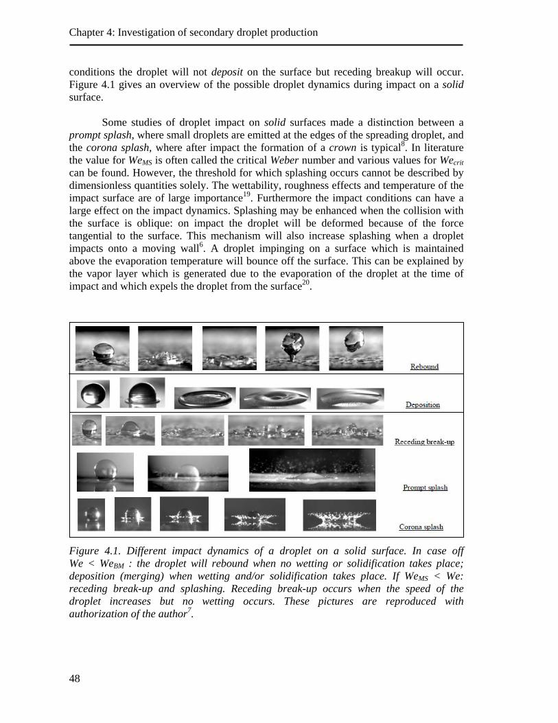
pattern is illuminated with UV radiation. The image is then demagnified by an optical system and projected onto the silicon wafer, which is covered with a photo-sensitive resist layer. Hence, the exposed parts of the photoresist layer are chemically altered. After the illumination, a different apparatus is employed to etch away the exposed (unexposed) parts of the positive (negative) photoresist layer and the pattern is etched into the top layer of the wafer. These patterns are further processed to form electronic pathways. A simplified way of this procedure is depicted in figure 1.3.
Figure 1.1. According to Moore’s law the number of transistors on an integrated circuit doubles roughly every two years. (source: Intel)
Figure 1.2. Principle of optical lithography
Chapter 1: General introduction
4
Figure 1.3. Simplified sketch of the illumination and processing of a wafer. (a)The wafer that is covered with a photoresist layer is illuminated in a lithography tool. (b) During exposure the photoresist becomes chemically altered. (c) In a different tool the (positive) photoresist and the wafer underneath can be selectively etched. (d) Electronic pathways or other structures can be created by deposition of various materials into the etched patterns.
The achievable minimum feature size of the imaging process is for a large part determined by the following properties of the optical lithography system: the resolution or linewidth Lw of a line projected onto a wafer and the depth of focus (DOF). A schematic representation of these quantities is depicted in figure 1.4. The resolution or the minimum linewidth Lw is determined by the numerical aperture NA and the light wavelength λ as4
1wL kNAλ
= (1.1)
with k1 a proportionality factor that has a limiting value of 0.25 for single exposure5. The numerical aperture NA is defined as NA = sin(θ), with θ the maximum allowed opening angle of the projection lens system.
The depth of focus (DOF) is an indication of the vertical distance around the focal plane for which the image will remain sharply in focus. The DOF is given by4
2 2DOF kNA
λ= (1.2)
where k2 is another proportionality constant. Figure 1.4 shows that minimum DOF is restricted by the thickness of the photoresist layer.
To improve the attainable resolution, three different methods can be used: reducing the imaging wavelength λ, increasing the numerical aperture and finally decreasing k1. All these methods have been employed in the past. To start with, we will discuss the reduction of the imaging wavelength.
Early lithography tools first made use of mercury arc lamps, emitting at 436 nm and later at 365 nm. With the development of excimer lasers operating in the deep ultraviolet (DUV) range, the wavelength was further reduced starting with the 248 nm krypton fluoride (KrF) wavelength. Currently, the argon fluoride (ArF) operating at 193
5
nm is state-of-the-art in commercially available systems. Reducing the wavelength even further is not trivial; the quartz lenses of the optical system need to be replaced as they absorb radiation below 193 nm. Furthermore, the tools need to operate in vacuum because ambient air starts to absorb the radiation significantly6.
Figure 1.4. Sketch of the quantities determining the minimum feature-size obtained with optical lithography. (a → b) If θ is increased, and hence the numerical aperture NA, the linewidth Lw reduces but DOF shrinks faster. (c) a shorter wavelength reduces Lw even further.
Alternatively, the resolution can be improved by increasing the numerical aperture
NA of the optical system. However, equation (1.2) shows that this reduces the DOF which makes vertical positioning of the wafer more critical. In addition, the thickness of the photoresist layer gives a lower limit to the DOF. Besides these practical limits, a fundamental limit is imposed by the fact that sin(θ) cannot be larger than unity. However, in recent years a new technology was developed that reduces the feature size of the 193 nm systems significantly. With the so-called immersion lithography the usual air gap between the projection lens and the wafer is replaced with a liquid with a refractive index nliq > 1. The numerical aperture is then often redefined as NA = nliq × sin(θ liq). This modified definition leads to a numerical aperture > 1, also called hyper-NA. Note that this newly defined NA cannot be substituted into equation (1.2). The depth of focus in this case then becomes DOF = k2∙λ / (nliq ·sin2θ).
Water based immersion lithography with hyper-NA = 1.35 and k1 = 0.27 can extend the 193 nm technology down to 40 nm[5]. Using high-index immersion fluids and optimization of the optical materials could decrease the resolution even further. Nevertheless, a limit for the achievable numerical aperture also exists with immersion lithography. In addition, developing new glass materials that meet the optical requirements and employing high refractive-index liquids poses significant technical and economic challenges.
Besides reducing the wavelength and increasing the numerical aperture, the value
of k1 can be decreased. Although k1 cannot be reduced below a fundamental limit of 0.25, double-patterning can be used to lower the effective k1 value5. With double-patterning the patterns of one mask are split into two less-dense mask patterns with k1 > 0.25. As a result, the wafer processing steps, as shown in figure 1.3, have to be performed for each different mask until the whole pattern is etched. In this way, optical lithography with an
Chapter 1: General introduction
6
effective k1 < 0.25 can be achieved. However, there are several challenges to this technique such as splitting the original pattern into two (or more) different layers and pattern-to-pattern overlay. In addition, because the lithography process has to be performed repeatedly to etch one single pattern, the processing cost and the cycle time increase.
With the 193 nm optical lithography technology reaching its boundaries, new
technologies are being developed to further reduce the minimal achievable feature size. These include maskless lithography, nano-imprint lithography and EUV lithography.
In maskless lithography, such as electron beam lithography, a focused beam of particles is employed to directly write the desired pattern onto a resist layer on the wafer such that there is no need for expensive masks. However, the throughput of these systems is currently limited to 1 wafer per 24 hours7. The goal is to reach a throughput of 10 wafers per hour8, whereas with optical lithography a throughput of more than 100 wafers per hour can be attained. Therefore, it is expected that maskless lithography will not be suited for high-volume manufacturing.
With nano-imprint lithography a low viscosity monomer (imprint resist) is deposited on the wafer. Subsequently, a template with predefined topological patterns is lowered into the fluid which then flows into the patterns. The monomer is then heated or exposed to UV light such that it is converted into a solid form, whereafter the template is removed. Hence, a wafer remains with a solid pattern printed on the surface. This technology allows obtaining feature sizes below 10 nm and is less expensive than optical lithography. However, defects and overlay are still critical issues to be resolved. Additionally, nano-imprint requires a mask-pattern ratio of 1:1 and mask availability becomes an increasing issue when going down in feature size.
It is expected that EUV lithography will be introduced to produce features smaller than 32 nm. This technology will make use of plasma light sources, which produce EUV radiation with a wavelength of 13.5 nm to project small-scale patterns onto wafers.
1.3 EUV lithography Extreme ultraviolet lithography using radiation of 13.5 nm is the next step in the downscaling of optical lithography tools. When reducing the wavelength of optical lithography below 193 nm, the problem is encountered that the low wavelength radiation is absorbed by air6 and that traditional lenses are not sufficiently transparent to EUV radiation. In addition, the light production mechanism changes from conventional lamps and lasers to pulsed light emitting plasmas of relatively high-temperature9.
As a result, vacuum operation of the lithographic tool is required and reflective optical elements have to be employed. To achieve good imaging resolution and small aberrations, the use of near-normal incidence mirrors has been proposed. These mirrors consist of alternating layers of silicon and molybdenum and are designed to work as Bragg reflectors. That is, the layers have different refractive indices and each is given a thickness of roughly half the wavelength. Constructive interference of the reflected light off each interface in the material leads to an acceptable reflectivity value. For a Mo/Si multilayer stack this reflectivity is about 70 % for a wavelength near 13.5 nm[4]. It is clear
7
that a minimum amount of reflections is desired to reduce the loss of the available radiation power.
A design example of an EUV lithography exposure tool is presented in figure 1.5. The EUV radiation emitted by a pulsed Sn-plasma with a relatively high temperature (Te = 30 eV) is partly collected by the collector mirror and focused into the so-called intermediate focus (IF) point. The required radiative power emitted by the source is usually defined as the power required in a 2% bandwidth around 13.5 nm at the IF. Currently, the required power is stated at 115 W at IF[10], although this requirement is susceptible to the development of the sensitivity of the photoresist. A more detailed description of EUV sources is given in chapter 2.
Figure 1.5. Design example of the optical system from an EUV lithography tool. The radiation emitted by the plasma is collected by the ‘Collector mirror’ and focused to the so-called intermediate focus, possibly after passing a ‘Spectral purity filter’. The condenser optics illuminate the reticle, which also serves as a mirror, and the image is projected onto the wafer with the projection optics.
1.4 Scope of the thesis Besides the desired EUV radiation these pulsed light emitting plasma sources also generate debris. The interaction of debris with the collector mirror results in reflection losses. The requirements of the industry specify a collector lifetime of about 1 year of source operation10; that is a maximum of 10 % reflection loss after roughly 1012 pulses. Therefore, the development of an efficient debris mitigation system, which is positioned between the plasma source and the collector optics to intercept the debris, has become one of the critical issues for EUV lithography. In addition, better understanding of the
Chapter 1: General introduction
8
mechanisms responsible for the debris production may result in reducing the debris emission while maintaining a maximum of EUV emission.
The scope of this work is to investigate the origin and nature of the debris produced by an EUV emitting Sn-based discharge produced plasma (DPP) source. Part of the work was focused on the mitigation of debris and various mitigation structures were tested. These experiments were documented and are not treated any further in this thesis11-12-13. The mitigation structures also proved to be useful as debris characterization tools and to distinguish between different kinds of debris. The debris can be divided into three different types: micro-particles or droplets, slow atomic/ionic debris and fast ionic debris. As the production mechanisms of the first two types of debris are inherently connected with the working principle of the DPP source, the focus of the work presented here is on the study of the fast ionic debris.
Lifetime measurements of the collector mirror are difficult to perform due to the long exposure times. In addition, to investigate the impact of the fast ionic debris on the collector a fully operational debris mitigation system needs to be installed to minimize the effect of the other kinds of debris. Therefore, various methods and tools are developed to measure the characteristics of the fast ionic debris without the need for long exposure times. Based on the EUV producing discharge dynamics, the production mechanisms of these high-energy ions are studied in more detail and some methods are proposed and experimentally validated to effectively suppress the production of the fast ionic debris.
1.5 Outline The following chapter describes the two different types of EUV producing plasma sources that are currently under consideration for EUV lithography: the laser produced plasma (LPP) source and the discharge produced plasma (DPP) source. In addition, the choice of the source fuel is discussed. In chapter 3 the different kinds of debris are studied and the impact on the collector optics is investigated. The different phases during the discharge process when the debris is produced are discussed and the relative amount of each type of debris to the total debris emission is estimated based on deposition experiments. In chapter 4, the impact of the micro-particles emitted by the DPP source on the surfaces found inside a source-collector module is studied. During impact of these droplets, so-called secondary droplets may be produced. A literature study is performed to study the impact dynamics of liquid Sn droplets on liquid and solid surfaces and experiments are conducted to investigate the possible production of these secondary droplets for representative conditions. In chapters 5 and 6 the characteristics of the ionic debris are investigated. First, two characterization tools are presented that are employed to measure the ion charge distribution and the ion energy distribution. These are determined using time-of-flight measurement with respectively an electrostatic ion energy analyzer and a Faraday cup configuration. In chapter 6 the region of production of the high-energy ions emitted by the DPP source is investigated using gated pinhole camera imaging. In addition, the nature of these ions is determined using mass-to-charge analysis.
9
The z-pinch dynamics of an Sn-based EUV emitting DPP source are studied in chapter 7. External parameters are identified which influence efficient pinch formation and the optimal settings of these parameters are experimentally determined. In chapter 8 the production mechanisms of the high-energy Sn ions are discussed. Based on the previously mentioned external parameters, some methods are proposed to prevent the formation the fast ionic debris.
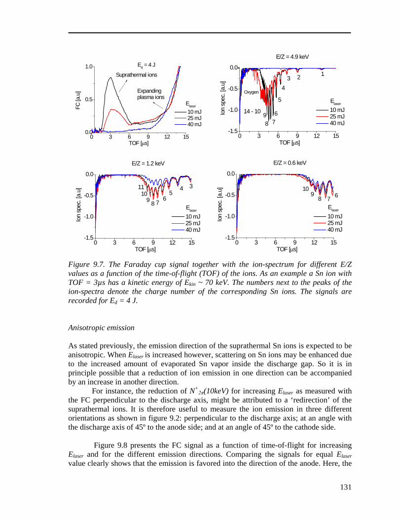
Finally, in chapter 9 two methods to suppress or prevent the production of the fast ionic debris are experimentally validated: increasing the initial Sn vapor distribution and adding hydrogen gas to the source chamber. During these experiments the EUV emission is monitored and a suppression factor for the high-energy Sn ions is determined. It is shown that with these methods, the production of high-energy Sn ions can be prevented.
Bibliography 1 E.R.Kieft, Transient behavior of EUV emitting discharge plasmas, Ph.D. thesis, Eindhoven University of Technology (2005) 2 M.H.L. van der Velden, Radiation generated plasmas: a challenge in modern lithography, Ph.D. thesis, Eindoven University of Technology (2008) 3 G.E. Moore, Electronics 38 (8), 114 -117 (1965) 4 D. Attwood. Soft X-Rays and Extreme Ultraviolet Radiation. Cambridge University Press, (1999) 5 N. Harned, F. van de Mast, Technology options for lithography at 32 nm, EuroAsia Semiconductor, October 2007, available online at www.euroasiasemiconductor.com 6 S.Nagai, K.Takehisa et.al., Development of a 2 kHz F2 Laser for 157 nm Lithography, Jpn. J. Appl. Phys. 38 70133 (1999) 7 D. McGrath, Initiative forms around e-beam direct write, EE Times, February 2009, available online at www.eetimes.com 8 A.F. Pele, TSMC joins Leti program on e-beam lithography, EE Times Europe, July 2009, available online at www.eetimes.com 9 V.Banine, R.Moors, Plasma sources for EUV lithography exposure tools, J. Phys. D: Appl. Phys. 37, 3207 (2004) 10 EUV sources for Lithography edited by V.Bakshi, Bellingham, Washington USA, SPIE Press (2006) 11 K.Gielissen, Characterization and mitigation of debris from a Sn-based EUV source, graduation thesis, Eindhoven University of Technology, The Netherlands (2005) 12 W.A.Soer, M.J.W. van Herpen, Microparticle mitigation concepts for high-volume EUV lithography, PR-TN 2007/00215, Philips Research, Eindhoven, The Netherlands (2007) 13 W.A.Soer, M.J.W. van Herpen, K.Gielissen, Debris emission and suppression in discharge-produced plasma EUV sources, PR-TN 2008/00067, Philips Research, Eindhoven, The Netherlands (2008)
Abstract The major lithography companies have established joint requirements for extreme ultraviolet (EUV) light sources. Two types of Sn-based plasma sources are under consideration for lithography purposes: laser produced plasma (LPP) sources and discharge produced plasma (DPP) sources. The work described in this thesis is devoted to the debris produced by the Sn-based DPP sources.
Chapter 2: EUV emitting plasma sources for lithography
12
2.1 Introduction Extreme ultraviolet (EUV) lithography is a possible candidate for the next-generation lithography tools that produce features smaller than 32 nm. This technology makes use of radiation in a small bandwidth around 13.5 nm. An overview of possible sources for this radiation is published in a special issue of the IEEE in 2004[1] and is partly summarized by Kieft2. These sources include among others synchrotron radiation3-4 and free electron lasers (FEL)5-6. Synchrotron radiation is frequently applied in EUV research and development, for example for the calibration of EUV sensors and the reflectivity measurements of multilayer (ML) mirrors. However, these types of sources are not regarded as potential light sources for lithography because they require huge capital investments and amounts of floor space.
The easiest and most cost-effective way to produce the desired EUV radiation is
to use atomic line radiation. In principle, transitions between excited levels of an atom or ion can only create photons with energies below the ionization potential of that atom or ion. Therefore, only multiply ionized atoms can produce line radiation with photon energies as high as 92 eV. Examples of atoms that have considerable emission spectra around 13.5 nm are lithium (Li), xenon (Xe) and tin (Sn). For example Li2+, Xe10+ and Sn8-12+ show emission peaks near the 13.5 nm wavelength. A sufficient amount of these ions can only be generated inside a hot plasma with temperatures between 20 eV and 50 eV. To excite the ions to the proper radiation levels, high electron densities on the order of 1025 m-3 are required.
In general, two different methods can be employed to supply the required energy
to a collection of atoms in order to generate a hot and dense EUV-emitting plasma. The first method is to focus an intense laser pulse onto a target. This type of plasma is called a laser produced plasma (LPP). The other method is to expose the target to a strong electric current such that the energy is supplied to the plasma through Ohmic heating. This kind of plasma is called a discharge produced plasma (DPP).
For both type of EUV sources, the sufficiently hot plasma is sustained only for a very short time due to the required input energy and the resulting heat load. Furthermore, it is not trivial to confine the plasma to the location where it has been created. The thermal energy of the particles is quickly converted into an expansion velocity. In addition to this energy loss, the particles themselves are lost because of the subsequent expansion of the plasma. Therefore, a pulsed operation of these plasma sources is required for efficient EUV production.
In this chapter the EUV emitting plasma sources are discussed that are currently
under consideration for use of lithography. The requirements of the industry are presented first followed by a discussion of the choice of Sn as the plasma fuel. Thereafter, the LPP and DPP source collector assembly are discussed separately.
13
2.2 Requirements from the industry The major players in the field of semiconductor lithography tools have defined a guide for the joint specifications for EUV sources for high volume manufacturing (HVM)7. These requirements are regularly updated to meet the current status of technology8. The requirements are summarized in table 2.1.
The in-band radiation is defined as the radiation in a 2% wavelength range around 13.5 nm. The 2% bandwidth is determined by the ML mirror transmission bandwidth. The required EUV power is generally specified at the intermediate focus (IF) position, as explained in chapter 1. Hence, this required power is independent of the precise source and collector optics designs.
The collection efficiency of the emitted EUV radiation is mainly determined by the collector optics. The solid angle of the emitted radiation of a light emitting plasma is always 4π sr. Dependent on the source characteristics this solid angle can only be partly covered with collector optics.
In addition to the collection efficiency of the collector optics, another constraint to the collection of the emitted radiation by the plasma is the so-called etendue. The etendue is an optical constant determined by the optical system. The source etendue is the integral of the collectable solid angle over the (effective) surface of the source2 (unit: mm2×sr). The importance can be described as follows: when light emitted from an optical system with etendue A (the light source) enters an optical system with etendue B < A, part of the light is not transmitted8. This light is transferred into thermal energy inside the optical system.
Thus, the best approach is to make the collected solid angle as large as possible and at the same time reduce the plasma size to match the etendue.
Table 2.1. The requirements of the EUV source as determined in 2006[7]. Of crucial importance is the in-band EUV power at IF. The required value, being still under dispute, will mainly depend on the sensitivity of the photoresist.
Source characteristics Requirements Wavelength (2 % bandwidth) 13.5 nm In-band EUV power at IF 115 W ( 180 W [8]) Etendue of source output ≤ 1 – 3.3 mm2 × sr[8] Spectral purity 130 – 400 nm ≤ 3 – 7 % of in-band > 400 nm to be determined Repetition frequency > 10 kHz Integrated energy stability ± 0.3 %, 3σ over 50 pulses Source cleanliness at IF ≥ 30.000 hours
Chapter 2: EUV emitting plasma sources for lithography
14
Apart from the in-band radiation, also out-of-band radiation is produced by the
plasma sources. This type of radiation may be partly transmitted through the optical system and it can influence the performance of the lithographic tool in different ways. First, the out-of-band radiation that is absorbed by the optical elements contributes to heating. The acceptable thermal load of these mirrors is determined by the cooling systems of the optical elements and the further development of the ML optics. In addition, the photoresist layers are not only sensitive for EUV radiation but also to light with longer wavelengths. Because of this, the image of the mask on the wafer will have a much worse resolution. To suppress the transmission of the out-of-band radiation, spectral purity filters are under development.
A high repetition frequency is another important requirement for the pulsed EUV emitting plasmas. This is not only necessary to achieve the required output power. As the EUV lithography tools are scanning systems, the high repetition frequency together with the integrated energy stability are necessary to ensure dose uniformity within an exposure field. The integrated energy stability is measured over 50 pulses and often some kind of pulse-to-pulse feedback mechanisms compensates for individual pulses that are stronger or weaker than average.
Finally, the source cleanliness is highly important. The plasma sources emit, besides the in-band and out-of-band radiation, particles that can damage the collector optics. These particles consist of thermal and non-thermal atoms and ions. For the case of a discharge plasma also droplets or clusters of the working material or from the electrode are emitted. This so-called “debris” needs to be intercepted or avoided being produced to prevent degradation of the collector optics or transmission into the optical system. The source cleanliness is generally expressed in hours of source operation before the collector optics reflectivity has decreased 10 %.
2.3 Fuel There are several elements that can generate emission spectra in the desired 13.5 nm radiation bandwidth, examples are xenon (Xe), lithium (Li) and tin (Sn). The choice of the element is mainly determined by the conversion efficiency (CE), that is the ratio between the useful radiation output versus the energy supplied to the plasma.
For the development of various types of EUV sources, Xe has been commonly applied as the working element. It has the advantage of being a noble gas. At ambient conditions it is in the gaseous state and additionally it is chemically inert. However, Xe10+ is the only emitter in the 13.5 nm bandwidth range and for a Xe plasma an CE of only 1 % is measured.
Because Li is a line emitter at 13.5 nm (Li2+), a Li EUV source produces less unwanted radiation and less heating than other sources. In addition, a conversion efficiency up to 3 % is observed9. However, Li is rather aggressive with a high diffusivity through the ML optics. As a result, deposition of Li irreversibly damages the collector mirror10. Several diffusion barrier materials have been investigated; however they currently lack thermal stability and good reflectivity9.
15
During the last years, the use of Sn as the working element has attracted increasing attention. Although it is solid at ambient temperatures and more effort needs to be put into protecting the collector mirror from being polluted, the EUV spectrum of Sn is more favorable than that of Xe. Multiple ionic stages, Sn8+ to Sn12+, contribute to the emission around 13.5 nm. An overview of the spectral lines of Xe and Sn can be found in literature11-12-13.
Since 2005, it is generally agreed that without multiplexing Xe-based DPP sources they cannot deliver the required radiation power for lithography purposes14. Additionally, Xe-based LPP is not feasible due to the required laser power and the resulting costs to produce sufficient EUV radiation. Nowadays, the attention is focused on the development of high power Sn-based DPP and LPP sources.
2.4 Laser produced plasma source The rather simple working principle of LPP sources is presented in figure 2.1. A multikilowatt CO2 laser of 10.6 μm is focused onto a Sn droplet of roughly 150 – 20 µm size. Due to absorption of the laser energy the droplet evaporates, ionizes and finally a hot expanding plasma is created that emits the desired EUV radiation. The working principle and models of the evolution of an LPP can be found in literature2,15-16. A ML coated normal-incidence collector mirror reflects roughly 5 sr of the emitted radiation to the IF point.
High power CO2 laser produced Sn plasma sources for lithography purposes are currently under development at Cymer17 and Gigophoton Inc.18. The critical issues of these kind of sources are Sn deposition on the collector and collector sputtering by Sn ions with energies of several keV. Additionally, the spectral purity is of high concern because of the reflection and scattering of the 10.6 μm laser light into the optical system19.
Figure 2.1. Sketch of a laser produced plasma (LPP) source. A powerful CO2 laser is focused onto a liquid Sn droplet to create the EUV emitting plasma. A multilayer coated collector mirror collects > 5 sr of the radiation initially emitted in a solid angle of 4π and the light is focused onto the so-called intermediate focus (IF) point.
Droplet generator
CO2 laser pulse
Collector > 5 sr IF
Chapter 2: EUV emitting plasma sources for lithography
16
2.5 Discharge produced plasma source A different method to create the hot and dense EUV emitting plasma is to make an electrical discharge inside a gaseous material. The plasma is heated by Ohmic dissipation of the current and through the current induced Lorentz force. This force also contracts the plasma and an increase in density is achieved by the so-called pinch effect. In chapter 7 the z-pinch dynamics of a Sn-based DPP source is discussed in more detail.
The DPP source also makes use of a laser but in contrast to the LPP this laser is only used to trigger the DPP and to dose the amount of Sn fuel. Typically, a Nd:YAG laser operating at a wavelength of 1064 nm is used to evaporate liquid Sn in between two rotating, Sn coated, electrodes. The electrodes are connected to a capacitor bank through a low-inductance circuit such that a large amount of electrical energy can be dissipated inside the plasma in a short time duration. The capacitor bank is connected to an external power supply in order to recharge after the current pulse. A schematic picture of the source-collector module is presented in figure 2.2.
For the case of DPP, part of the emitted radiation may be blocked by the electrodes or other parts of the source. In between the plasma and the collector optics a set of blades, the so-called foil trap, is positioned to prevent the Sn debris from reaching the collector. The collector optics consist of a number of quasi cylindrical grazing-incidence mirrors which are positioned concentrically. Hence, about 3 sr of the emitted radiation in 4π sr can be collected.
The laser triggered discharge plasma in Sn vapor is under consideration for use as light source in EUV lithography. These kind of sources are under development by Philips Extreme UV in cooperation with XTREME technologies20. The critical issues are the Sn deposition on the collector and collector sputtering by the Sn ions with energies of several tens of keV[19].
. Figure 2.2. Sketch of the source-collector module of a discharge produced plasma source. Sn coated rotating electrodes are connected to a capacitor bank C. The EUV emitting plasma is created by means of a strong electric current through Sn vapor. A set of blades, the so-called foil trap, protects the collector optics from the debris. The collector mirror collects ~ 3 sr of the emitted radiation.
Foil trap Collector ~ 3 sr (Cylindrical with multiple shells)
IF
Sn coated rotating electrodes
C
Sn evaporating Laser pulse
17
2.6 DPP versus LPP
An overview of the EUV source technology, requirements and limits is given by Bakshi21-22. Table 2.2 shows the required input power to obtain 150 W in-band EUV power at IF. The required plasma input power is the minimum power that needs to be supplied to the plasma to achieve sufficient in-band EUV at IF. Note that the wall plug power is determined by the efficiency of the plasma excitation apparatus, that is for LPP mainly determined by the efficiency of the CO2 laser and for DPP the efficiency of the high-voltage generator and the capacitor bank. For CO2 lasers the wall plug efficiency is about 8 %[21] while for DPP sources we estimate an efficiency of 50 %. Although less plasma input power needs to be supplied to the plasma of LPP sources, roughly three times more electrical energy is required to deliver 150 W in-band EUV power.
The lower required plasma input power for LPP systems is mainly due to the larger collection ability and the absence of debris mitigation structures.
Table 2.2 Comparison of the limits for Sn-based LPP and DPP sources for lithography22.
LPP DPP Wall plug power (W) 190000 60000 Wall plug efficiency (%) ~ 8 ~ 50 Plasma input power (W) 15000 30000 Conversion efficiency (% into 2π) 3 3 EUV power at the source (W) 450 900 Collection in sr (out of 2π sr) 5 3.14 Collection ability (% of 2π) 80 50 Collector transmission (%) 70 70 Debris mitigation transmission (%) 100 80 Gas transmission (%) 85 85 SPF transmission (%) 70 70 Etendue match (%) 100 100 Effective collection capability (%) 33 17 Power at IF (W) 150 150
The main concern of DPP sources is related to power scaling. A large amount of
heat must be dissipated close to the electrodes surfaces and in the source system. However, the DPP source manufacturers have shown the feasibility of 40 kHz source operation20. Additionally, the electrodes are cooled using an external circuit that continuously pumps the liquid Sn though a cooler module.
Chapter 2: EUV emitting plasma sources for lithography
18
Other important issues for choosing a suitable EUV source for lithography are the shape and size of the EUV emitting region8. The smaller and not so elongated size of the LPP enables better collection efficiency and flexibility in illumination settings. Furthermore, the LPP source technology makes use of mass-limited targets. This limits the consumption of Sn during long-term source operation. However, in chapter 3 we will show that a DPP source emits about 8 × 10¹⁵ Sn atoms in each single pulse, that is without optimization of debris production mechanisms. This corresponds to the amount of Sn atoms inside a droplet of roughly 75 µm in size. Thus, as long as LPP sources make use of Sn droplets > 75 µm, more Sn is consumed per LPP pulse than per DPP pulse.
Although both types of plasma sources show an increase in their performance,
many challenges still exist. The collector lifetime is one of the crucial issues for both LPP as DPP sources. Besides increasing the power output of the plasma sources, investigating the debris production processes are of crucial importance. In the next chapter an overview is presented of the different types of debris produced by Sn-based DPP sources.
19
Bibliography 1 D.T. Attwood, H.M. Hertz, K. Midorikawa, and M. Obara, Introduction to the issue on short wavelength and EUV lasers, IEEE J. Sel. Top. Quantum Electron. 10(6), 1241-1243 (2004) 2 E.R.Kieft, Transient behavior of EUV emitting discharge plasmas, Ph.D. thesis, Eindhoven University of Technology (2005) 3 D.T. Attwood, P. Naulleau et.al., Tunable coherent radiation in the soft X-ray and extreme ultraviolet spectral regions, IEEE J. Quantum electr. 35 (5), 709-720 (1999) 4 H.H. Solak, Nanolithography with coherent extreme ultraviolet light, J. Phys. D:Appl. Phys. 39 R171-R188 (2006) 5 M. Richter, A. Gottwald et. al., Measurement of gigawatt radiation pulses from a vacuum and extreme ultraviolet free-electron laser, Appl. Phys. Lett. 83 (14) 2970-2972 (2003) 6 C.Pellegrini and S.Reiche, The Development of X-ray Free-Electron Lasers, IEEE J. Sel. Top. Quantum Electron. 10(6), 1393-1404 (2004) 7 K.Ota, Y. Watanabe, V.Banine, H.Franken, EUV Source Requirements for EUV Lithography, Chapter 2 in EUV sources for Lithography edited by V.Bakshi, Bellingham, Wash.SPIE Press, (2006) 8 V.Banine, O.Frijns, G.Swinkels, Requirements and prospects of next generation EUV sources for lithography applications, International EUVL Symposium, Sapporo, Japan, Oct. 29-31 (2007) 9 I. Fomenkov, Feasibility of Updated Source Requirements, EUV Source Workshop, International EUVL Symposium, San Diego USA, Nov. 10 (2005) 10 D. Ruzic, Progress towards Sn DPP and LPP solutions: A source/collector perspective, International EUVL Symposium, San diego, USA Nov. 7-9 (2005) 11 J. D. Gillaspy, Atomic Xenon data, Chapter 3 in EUV sources for Lithography edited by V.Bakshi, Bellingham, Wash.SPIE Press, (2006) 12 I.Y. Tolstikhina, S.S. Churilov, A.N. Ryabtsev, K.N. Koshelev, Atomic Tin data, Chapter 4 in EUV sources for Lithography edited by V.Bakshi, Bellingham, Wash.SPIE Press, (2006) 13 T. Krucken, K. Bergmann, L. Juschkin, R. Lebert, Fundamentals and limits for the EUV emission of pinch plasma sources for EUV lithography, J. Phys. D:Appl. Phys. 37, 3213-3224 (2004) 14 V. Bakshi, EUV source technology status, EUV Source Workshop, International EUVL Symposium, San Diego USA, Nov. 10 (2005) 15 K. Garloff, J. Jonkers, M. van den Donker, R. Brummans, F. van Goor, J. van der Mullen, Simple model for laser-produced, mass-limited water-droplet plasmas, Phys. Rev. E 66, 036403 (2002) 16 M. Al-Rabban, M. Richardson, H.Scott, F.Gilleron, M.Poirier, T.Blenski, Modeling LPP sources, Chapter 10 in EUV sources for Lithography edited by V.Bakshi, Bellingham, Wash.SPIE Press, (2006) 17 D.C. Brandt, I.V.Fomenkov et.al., International EUVL Symposium, Lake Tahoe, USA Sept. 28 – Oct. 1, (2008) 18 A. Endo, Y.Ueno, et.al., International EUVL Symposium, Lake Tahoe, USA Sept. 28 – Oct. 1, (2008) 19 J.Benschop, V.Banine, S.Lok, E.Loopstra, Extreme ultraviolet lithography: Status and prospects, J. Vac. Sci. Technol. B 26 (6), 2204-2207 (2008) 20 M. Corthout, M.Yoshioka, et.al., International EUVL Symposium, Lake Tahoe, USA Sept. 28 – Oct. 1, (2008) 21 EUV sources for Lithography edited by V.Bakshi, Bellingham, Washington USA, SPIE Press (2006) 22 EUV lithography edited by V. Bashi, Bellingham, Washington USA, SPIE Press (2009)
21
Chapter 3
3 Debris produced by Sn-based DPP sources
Abstract
Generally the debris generated by discharge produced plasma sources can be divided into three different types: the micro-particles or liquid Sn droplets, the slow atomic and ionic debris and finally the fast ionic debris*
* The fast ionic debris is also referred to as the high-energy Sn ions or suprathermal Sn ions throughout this thesis.
. The origin of these kinds of debris is investigated and the impact on the collector optics is discussed. The relative amount of their contribution to the total debris emission is estimated on the basis of deposition experiments. In addition, the surface morphology of a deposited Sn layer on top of a Ru surface is visualized. Finally, the debris-producing phases during the discharge process are discussed.
Chapter 3: Debris produced by Sn-based DPP sources
22
3.1 Introduction Besides the desired EUV radiation, the Sn-based Discharge Produced Plasma (DPP) source generates debris that can damage the collector optics. This results in a decrease of the EUV reflection and thus a reduction of the available EUV power.
In general one can distinguish three types of debris: micro-particles or droplets, slow atomic-ionic debris and fast ionic debris. For each debris type the detailed effect on the optics is different, but they all result in reflection losses. The micro-particles, also called particulates or droplets, will result in a non-uniform surface coverage. The slow atomic-ionic debris will deposit on the collector mirror, which results in a quasi-uniform surface coverage, while the fast ionic debris results in both sputtering of and implantation into the surface.
Each type of Sn debris has specific production mechanisms and regions in which they are produced. The next section discusses the origin of all the different types of debris. After this, the characteristics of the different Sn debris types and their effect on the collector surface are discussed in subsequent sections. Finally, an overview is presented of the different kinds of Sn debris and their corresponding production mechanisms. For clarity and completeness, some of the results from experiments discussed in the following chapters are incorporated into this overview.
3.2. Origin of the debris The various kinds of debris originate from different places and at different times during the discharge process. The main causes for the creation of Sn debris are the laser pulse interaction with the liquid Sn on the cathode surface, the interaction of the discharge plasma with the electrodes surfaces, plasma instabilities during or just after the pinch phase and finally the expansion of the quenching plasma.
In addition to Sn, other elements may be present among the debris, these include electrode material and Sn contamination. These elements are introduced by means of electrode erosion or contamination of the liquid Sn. After this subsection, the study of debris is mainly devoted to the Sn based debris.
23
3.2.1 Sn-based debris The micro-particles or droplets are produced by the laser evaporation of the liquid Sn1-2-3 and by plasma-created cathode spots4-5-6-7-8. Droplets from cathode spots are believed to be produced due to the high plasma pressure on the liquid electrode surface9-10. Based on the latter mechanisms it is conceivable that droplets are also produced during the pinch phase of the plasma. Because of the compression of the plasma during the pinch phase, a lot of the plasma material is pushed away in the axial direction. The resulting ion bombardment on the electrodes can lead to the creation and ejection of micro-particles from the liquid electrode surface.
The slow atomic-ionic debris originates from the discharge plasma. After the pinch phase the plasma expands and decays into vacuum. Another source of slow atomic-ionic debris is a second, much cooler plasma. This plasma is observed after the pinch phase and is believed to be produced due to the heating of the liquid Sn on the cathode surface11.
The fast ionic debris is expected to be formed within the discharge gap during the pinch phase of the plasma. Generally Sn ions with kinetic energy Ekin > 10 keV emitted by the DPP source are denoted as fast ionic debris. Some production mechanisms of these high-energy ions are known and discussed in literature12. These mechanisms include compressional heating and the resulting ejection of suprathermal particles from the ends of the micropinch and acceleration of Sn ions due to the formation of high-inductive fields near the cathode or near the anode. An investigation of the production regions of these high-energy ions will be presented in chapter 6. It will be shown that they originate from a region close to the cathode surface as well as near the anode surface. Thus, a single production mechanism concerning extreme plasma conditions near the pinch region is not sufficient. These results support the reasoning that multiple production mechanisms act simultaneously. An analysis of the production mechanisms will be presented in chapter 8. Two methods to prevent these production mechanisms will be proposed: increasing the initial Sn distribution inside the discharge gap and add hydrogen gas to the source chamber. The resulting suppression factor of these methods was experimentally determined and will be presented in chapter 9.
3.2.1 Electrode erosion For the experiments presented in this thesis, two configurations of Sn-based DPP sources were employed: a source consisting of two rotating disk electrodes and one consisting of fixed electrodes. The operation principle for both types of sources is similar but for the debris production there is a significant difference.
This difference is mainly determined by the erosion of the fixed electrodes; a bath filled with liquid Sn acts as the cathode surface from which Sn is evaporated after which it expands to the anode. The solid metal anode will erode because of the large heat load from the discharge plasma13-14. Therefore, the evaporated anode material will also be detected along with the Sn-debris. Furthermore, it is not expected that droplets are
Chapter 3: Debris produced by Sn-based DPP sources
24
emitted from the anode surface. The evaporation of Sn from the cathode surface and the erosion of the anode imply that electrode material is consumed, which results in a steadily increasing electrode gap. This limits the number of consecutive discharges at which the source can operate while having a stable discharge.
Figure 3.1 gives a sketch of the fixed electrodes before and after an experiment of 2 × 10⁵ discharge pulses. The Sn layer on the cathode surface is consumed during operation, increasing the discharge gap. Moreover, a large crater can be observed at the anode surface.
Although the use of the DPP source with fixed electrodes leads to specific problems concerning source operation and debris contamination with anode material; the source is very suitable for debris analysis experiments. The three different types of Sn debris are produced by the same mechanisms, the discharge plasma is more easily accessed and the setup is very flexible. Thus, this type of source will be used during some experiments, especially when there is a necessity to place a setup close to the discharge plasma. Figure 3.1. Sketch of the fixed electrode configuration before and after 2 × 10⁵ discharges. The liquid Sn on the cathode surface has decreased significantly and a crater can be observed on the anode surface.
The source with rotating disk electrodes overcomes the issues of the fixed electrodes. During operation the disks rotate through a bath filled with liquid Sn. Hence, the surface of the electrodes is continuously covered with a layer of liquid Sn. As a result the heat load is divided across a larger surface area and electrode erosion is prevented. Moreover, the evaporated Sn from the cathode surface is replenished by means of rotation trough the Sn bath. Thus, the repetition frequency and the number of consecutive pulses during one experiment can be increased. This principle of operation is also used for high power Sn-based DPP sources15. Therefore this study on debris is mainly devoted to the debris produced by the rotating disk source.
Anode
Liquid Sn
Cathode
Start of experiment End of experiment
25
3.2.3 Contamination of Sn It is conceivable that small amounts of oxygen are temporarily present in the debris. Because the Sn baths are regularly exposed to air when venting the vacuum chamber in between experiments, a layer of SnO and SnO2 grows on the liquid Sn surface16-17-18-19-20. The oxygen is then introduced into the discharge plasma by means of evaporation of oxidized liquid Sn from the cathode surface by the laser. The oxidation rate increases with temperature, and even more rapidly for temperatures above the melting temperature of Sn. Thus, oxidation can be reduced by venting the source chamber only when the temperature of the Sn baths has decreased down to room temperature.
3.3 Micro-particles The micro-particles or droplets generated by the Sn-based DPP source form the first type of debris that will be discussed. This kind of debris is often referred to as droplets or particulate debris. The droplets are expected to originate from the electrode surfaces. The mechanisms responsible for the droplet generation are expected to be the laser interaction with the liquid Sn1-3 and the cathode or anode spots4-10. The droplets are ballistic in nature and their direction of motion generally overlaps with EUV photons. The droplets may deposit onto the EUV collector optics and this results in a locally non-uniform surface coverage.
3.3.1 Introduction The Sn droplets have sizes from several tens of µm down to 0.1 µm. Generally, the largest droplets have the lowest velocity; ranging from below 20 m/s for the large droplets, up to 700 m/s for the smallest ones. Mass deposition experiments showed that the droplets are responsible for about 50 % of the total emitted debris21.
Because the collector mirror reflects light at grazing incidence22 the presence of one droplet results in an effective coverage that is larger than the actual size of the droplet. Figure 3.2 gives a sketch of the situation at 10º grazing incidence. The shadow of the droplet increases the effective coverage ratio 5.7 times. Thus, the EUV photons will experience a coverage that is about 5 × higher than the droplet size itself.
Figure 3.2. Sketch of the increased effective coverage ratio of a deposited droplet due to the grazing incidence angle of 10º.
Chapter 3: Debris produced by Sn-based DPP sources
26
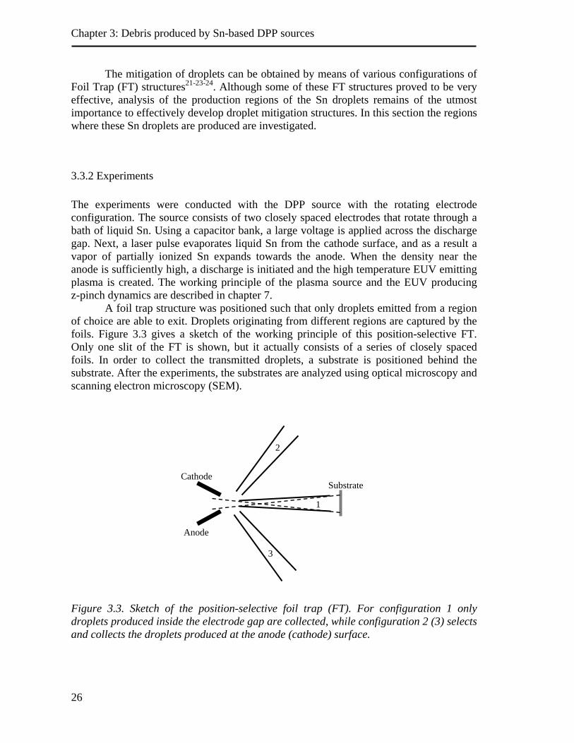
The mitigation of droplets can be obtained by means of various configurations of Foil Trap (FT) structures21-23-24. Although some of these FT structures proved to be very effective, analysis of the production regions of the Sn droplets remains of the utmost importance to effectively develop droplet mitigation structures. In this section the regions where these Sn droplets are produced are investigated.
3.3.2 Experiments The experiments were conducted with the DPP source with the rotating electrode configuration. The source consists of two closely spaced electrodes that rotate through a bath of liquid Sn. Using a capacitor bank, a large voltage is applied across the discharge gap. Next, a laser pulse evaporates liquid Sn from the cathode surface, and as a result a vapor of partially ionized Sn expands towards the anode. When the density near the anode is sufficiently high, a discharge is initiated and the high temperature EUV emitting plasma is created. The working principle of the plasma source and the EUV producing z-pinch dynamics are described in chapter 7.
A foil trap structure was positioned such that only droplets emitted from a region of choice are able to exit. Droplets originating from different regions are captured by the foils. Figure 3.3 gives a sketch of the working principle of this position-selective FT. Only one slit of the FT is shown, but it actually consists of a series of closely spaced foils. In order to collect the transmitted droplets, a substrate is positioned behind the substrate. After the experiments, the substrates are analyzed using optical microscopy and scanning electron microscopy (SEM).
Figure 3.3. Sketch of the position-selective foil trap (FT). For configuration 1 only droplets produced inside the electrode gap are collected, while configuration 2 (3) selects and collects the droplets produced at the anode (cathode) surface.
3
Substrate Cathode
Anode
1
2
27
The experiments were conducted for three different FT configurations. For configuration 1, the FT is positioned such that only droplets originating from inside the electrode gap are transmitted. Droplets emitted from the electrode surfaces are captured by the foils. For this configuration, no droplets are expected to be found on the substrate. For configuration 2, only droplets produced at the anode surface are collected, and finally for configuration 3 only droplets emitted from the cathode surface are transmitted by the FT.
3.3.2 Results First, the optical microscope images are analyzed. Figure 3.4 presents the corresponding pictures of the four different experiments. The top left picture is from the substrate of configuration 1, which is exposed to 4 × 10⁵ discharge pulses. As expected, no droplets are observed on the substrate. Moreover, the droplets produced at the electrode surfaces are effectively stopped by this FT configuration. So we may expect that with configuration 2 and 3 only droplets from the corresponding regions are transmitted by the FT.
The top right picture shows substrate from configuration 2. It is exposed to 105 discharge pulses, and only droplets emitted from the anode are collected. The maximum droplet size equals 10 µm. The bottom left picture shows the droplets collected with configuration 3, i.e. droplets emitted from the cathode surface during 105 discharges. The maximum size of these droplets is roughly 70 µm which is significantly larger than the droplets produced at the anode surface. The bottom right picture shows the droplets produced by the laser interaction with the cathode surface solely, that is in the absence of a plasma. These droplets have sizes up to roughly 50 µm.
Images of the substrates are also made using a Scanning Electron Microscope
(SEM). These SEM images are analyzed using software that counts the droplets according to their size25. Contrary to the optical images that show the larger part of the exposed substrate, the SEM images visualize only a small fraction of this area. Because the droplet distribution varied substantially between the different SEM images, the results of the different setup configurations proved difficult to compare.
Nonetheless, a representative droplet size-distribution is shown in figure 3.5. The droplet size-distribution of droplets emitted from the anode surface for 106 discharges is presented. The surface coverage of the substrate equals to about 50 %. The number of droplets decreases quasi exponentially to sizes of 4 µm. The low density of droplets > 4 µm is mainly due to the small area that is imaged with the SEM.
Chapter 3: Debris produced by Sn-based DPP sources
28
Figure 3.4. These pictures show the different substrates exposed for the 3 FT configurations. (top left) Configuration 1, it is shown that no droplets originate from the region inside the discharge gap. (top right) Configuration 2, droplets emitted from the anode surface during the discharge. (bottom left) Configuration 3, droplets emitted from the cathode surface by the laser and during the discharge. (bottom right) Configuration 3, droplets emitted from the cathode surface solely by the laser; no discharge is initiated.
0 2 4 6 8 10
10
100
1000
# dr
ople
ts /
106 d
ischa
rges
Droplet size [µm]
Typical droplet size distribution
Figure 3.5. Typical droplet size-distribution of the droplets emitted from the anode surface of the Sn-based DPP. The graph shows the droplets for 106 discharges.
Configuration 1: Between the electrodes Configuration 2: Anode
Configuration 3: Cathode Configuration 3: Cathode, only laser no discharge
100 µm
29
3.3.3 Discussion The images from figure 3.4 show that a significant amount of droplets is emitted from the cathode surface due to the Sn evaporating laser pulse solely. To isolate and investigate the influence of the laser on the droplet emission, the laser settings can be altered. However, the laser pulse should primarily be optimized for stable discharge dynamics and the maximum amount of EUV output.
The droplets emitted from the cathode surface increase in number and size when the laser pulse is accompanied by the subsequent discharge plasma. Furthermore, it is shown that the emission of droplets is not limited to the cathode surface. A large number of droplets are also emitted from the anode surface, although these are generally smaller in size. As expected, no droplets originate from the region in between the electrodes.
The droplets emitted from the cathode have diameters up to 70 µm, while the droplets from the anode have sizes up to 10 µm. A quantitative comparison of the droplet size distribution proved to be impossible because of small misalignments of the FT. Nonetheless, for both electrodes it is found that for the range 0.1 µm < droplet diameter < 4 µm, the number of droplets decreases quasi exponentially with their size.
Because the droplets emitted from the cathode surface are generally larger in size, it is expected that the mass distribution of the particulate debris is anisotropic. This has to be accounted for when designing mitigation structures to prevent the droplet deposition on the collector surface. It should be noted, that the size of the droplets that is measured during these experiments, is actually the diameter of the resulting splat on the surface. The size of the splat is mainly determined by the wetting conditions and the solidification time of the liquid Sn droplets on the substrate surface. From the optical microscope images shown in figure 3.4, as well as from the SEM images, the height of the splat is difficult to estimate. Thus, a calculation of the contribution of Sn droplets to the deposited mass, based on the size of the splats, is subject to large uncertainties. However, for the discharge source with fixed electrodes the mass contribution of the droplets was measured21 and equals about 50 %. When the liquid Sn droplets impact upon the surfaces inside the vacuum chamber, so-called secondary droplets may be produced. These secondary droplets originate from various places inside the vacuum chamber, and are therefore very hard to mitigate. In chapter 4, the impact dynamics of the liquid Sn droplets are investigated.
3.4 Slow atomic/ionic debris
3.4.1 Introduction Slow atomic-ionic debris consists of neutral atoms and low energy ions. Contrary to the droplets that are created at the electrode surfaces, these particles mainly originate from the discharge plasma. Besides that, a second much cooler plasma is observed after the pinch phase11, and this plasma may also contribute to the slow atomic/ionic debris emission. The expansion dynamics closely resemble the dynamics of an expanding laser ablation plume. The latter are extensively described in literature26-27-28.
Chapter 3: Debris produced by Sn-based DPP sources
30
It is expected that this kind of debris is thermalized. Thus, the particles have randomized directions and velocities forming a Maxwell velocity distribution. The deposition on the collector of this kind of debris, gives a quasi-uniform surface coverage. The reflection loss due to 1 nm of Sn on a Ru mirror equals to 14% for a 10º angle of incidence29. A series of experiments was conducted to investigate the deposition characteristics of the atomic/ionic debris. Substrates were exposed to the DPP source at vacuum conditions. SEM analysis was performed to show the surface morphology, and with X-ray Fluorescence (XRF) the amount of deposited Sn is determined. In addition, with Atomic Force Microscopy (AFM) the surface morphology of the exposed substrate was investigated. From these experiments, the amount of Sn particles emitted by the DPP source and contributing to deposition can be calculated.
3.4.2 Experiments Two Si substrates are placed inside the vacuum chamber for exposure. Figure 3.6 gives a sketch of the setup. The substrate S1 is placed at a distance of 115 mm from the plasma. This substrate is subjected to all kinds of debris: droplets, slow atomic/ionic debris and fast ions. A second Si substrate S2 is placed next to the electrodes, so that it does not coincide with the direct line-of-sight of the plasma. It is expected that only thermalized atoms or ions can deposit on substrate S2. However, it is also possible that some energetic particles reflect from the vacuum chamber wall behind substrate S1 and subsequently deposit on substrate S2. The arrows in figure 3.6 indicate the possible directions of the atomic and ionic debris.
The substrates are exposed simultaneously to 1.6 × 10⁵ discharge pulses at vacuum conditions ( p ~ 10-3 Pa). The source settings during exposure are Ed = 4 J and Elaser = 40 mJ. Finally, both substrates are analyzed using SEM images and XRF measurements. Figure 3.6. Top-view sketch of the deposition experiment. The Si substrate S1 is directly exposed to the source and is subject to deposition and sputtering. The Si substrate S2 is placed outside the ‘line of sight’ of the plasma. The arrows indicate the possible directions of the atomic and ionic debris.
S1
Cathode
Anode
S2
Deposition + sputtering
Reflection vacuum chamber wall
31
3.4.3 Results A typical SEM image of substrate S1 is presented in figure 3.7. This substrate is directly exposed to the discharge plasma. As a result, splashes of Sn droplets as large as 10 µm are visible. Besides the splashes, the surface of the substrate is covered with a quasi uniform layer of Sn. This layer is not smooth however; a chaotic pattern of ‘grains’ of several micrometers in size are visible. Some droplets, which may have been deposited at the beginning of the exposure, are being overgrown by these ‘grains’.
Figure 3.7. SEM image of the substrate S1 directly exposed to the plasma. Large splashes of Sn droplets are clearly visible upon a background of deposited atomic/ionic debris. An average Sn layer with a thickness of 220 nm Sn is measured with XRF.
Figure 3.8. SEM image of the Si substrate S2 placed out of the line-of-sight of the plasma (see fig. 3.6). An average Sn layer with a thickness of 55 nm is measured with XRF.
Chapter 3: Debris produced by Sn-based DPP sources
32
By means of XRF analysis it is found that a Sn layer with an average thickness of about 220 nm is deposited upon the substrate S1. We recall that about 50 % of the emitted debris consists of liquid Sn droplets21. Thus, the Sn layer created by atomic/ionic debris is estimated to equal 110 nm effectively.
Figure 3.8 presents a SEM image of substrate S2, which was placed out of the line of sight of the plasma source. As expected, no Sn droplets are found on the surface. However, ‘crystal’ shaped structures with sizes up to 5 µm can be observed. In contrast to the ‘grains’ seen in figure 3.7, these ‘crystals’ have sharp edges and in general do not touch each other. Furthermore, with XRF analysis an average Sn layer with a thickness of 55 nm is found upon the surface. Because droplets are not found on substrate S2, a correction for the deposition thickness is not necessary.
The deposition of Sn on the surface of substrate S2 may originate from two different mechanisms. First, as the slow atomic/ionic debris is thermalized, the particles have randomized directions. As a result, deposition may occur on surfaces not directly exposed to the plasma. Second, the substrate S1 was positioned directly in front of the vacuum chamber wall, i.e. a stainless steel surface of roughly 30 cm in diameter. It is possible that the more energetic atomic/ionic particles have reflected upon this surface towards substrate S2. A sketch of the particle directions is shown in figure 3.6.
There is a significant difference in the surface morphology of substrates S1 and S2 shown in figures 3.7 and 3.8 respectively. Although substrate S2 is placed out of the direct line-of-sight of the plasma, the difference in morphology may be explained by a difference in Sn coverage solely. Substrate S1 has a Sn layer thickness of 220 nm, while S2 only has an average layer thickness of 55 nm.
In the following subsection, the surface morphology is investigated for substrates which have a different thickness of Sn, that is deposited during exposure in the direct line-of-sight of the plasma.
3.4.4 Surface morphology The formation of the ‘crystals’ by means of Sn deposition, as shown in figure 3.8, is confirmed during other experiments. This effect is observed for both Silicon and Ruthenium substrates exposed to the Sn-based DPP source at vacuum conditions. In order to further investigate the surface morphology, two Ru substrates with different average layer thickness have been analyzed using Atomic Force Microscopy (AFM)30.
Figure 3.9 shows the AFM scans of a Ru substrate with an average Sn layer deposition of 9 nm. Some large crystals of a couple of micrometers in size are visible on the surface. The growth of these crystals can be attributed to the reduction of surface energy as a driving force. This combined with a high mobility of Sn on the substrate may give rise to the crystal formation. In between of the crystals hemispherical particles of about 100 nm in size are found. These are confirmed to be Sn by Auger analysis.
Figure 3.10 shows the AFM scans of a Ru substrate with on average 53 nm of Sn on top. Here, the density of the large Sn crystals is substantially larger and the smaller particles are so densely spaced that they almost cover the whole surface. It is expected
33
that when the Sn deposition increases even further, identical structures as seen on figure 3.7 will be visible.
Thus, the chaotic pattern of ‘grains’ found in figure 3.7 is a combination of superposition of the increasing density of the crystals and the growing hemispherical particles.
Figure 3.9. AFM scans of a Ru substrate with an average Sn deposition of 9 nm. The deposition is obtained by direct exposure to the Sn-based DPP source.
Figure 3.10. AFM scans of a Ru substrate with an average Sn deposition of 53 nm. The deposition is obtained by direct exposure to the Sn-based DPP source. AFM analysis is performed at Philips Research30.
Chapter 3: Debris produced by Sn-based DPP sources
34
3.4.5 Discussion The average Sn layer thickness deposited during 1.6 × 10⁵ discharge pulses equals to about 220 nm. The fraction attributed to the slow/atomic ionic debris equals 50 %, which corresponds to an average layer of 110 nm. The deposition is measured perpendicular to the discharge axis. Assuming that the slow atomic/ionic debris emission is isotropic, this corresponds to an emission of 4 × 10¹⁵ Sn particles per pulse in a solid angle of 4π.
In chapter 5 the number of emitted slow ionic debris particles, more specifically Sn ions with Ekin < 10 keV, will be calculated based on Faraday cup measurements of the expanding Sn plasma. About 1014 Sn ions are emitted in a solid angle of 2π. From this it can be concluded that 95 % of the slow atomic/ionic debris deposition is atomic in nature, and that only 5 % is due to ions.
However, initially only 2 - 5 × 10¹⁴ Sn particles are evaporated inside the discharge gap by the laser pulse34. This is one order of magnitude lower than the total number of slow atomic and ionic Sn particles as measured during the deposition experiments. This difference may be attributed to additional Sn evaporation because of the heating of the electrodes and a larger contribution of the Sn droplets to the total amount of deposited mass. The debris emission is also expected to be anisotropic due to the electrode configuration and the magnetic field generated by the z-pinch current.
Concluding, the quasi-uniform deposited Sn layer on substrate S1 is one order of magnitude higher than the total amount of Sn initially evaporated by the laser pulse. The latter however, corresponds well with the number of emitted low energy ions. Assuming that about 50 % of the deposited material is attributed to Sn droplets, an average of 4 × 10¹⁵ Sn particles are emitted per pulse by the DPP in a solid angle of 4π. Furthermore, Sn deposition is observed on surfaces not directly exposed to the plasma. This deposition may be due the randomized directions of the low energetic debris, or more likely as a result of the reflection of high energetic particles from the vacuum chamber wall. Even so, it shows the importance of an additional debris shield for crucial structures inside the vacuum chamber.
Furthermore, it is found that when the average Sn layer thickness is smaller than 50 nm, the deposited Sn is concentrated in micrometer sized crystals and smaller hemispherical particles. As a result, the coverage is quasi-uniform.
35
3.5 Fast ionic debris The fast ionic debris mainly consists of high-energy Sn ions emitted by the discharge plasma. They originate from the discharge plasma. In chapter 5 it will be shown that these high-energy ions are suprathermal†
, and in chapter 6 the region of generation of these ions will be investigated. It is found that these ions not only originate from the pinch region, i.e. close to the cathode surface with locally extreme plasma conditions, but also from a region close to the anode surface. The high-energy Sn ions may be produced by different production mechanisms that act simultaneously. These mechanisms include, among others, compressional plasma heating and ion acceleration due to the formation of high-inductive electric fields. An analysis of some production mechanisms is presented in chapter 8. The present section discusses the result of the impact of fast ionic debris on the collector surface.
3.5.1 Introduction The characteristics of the fast ionic debris will be investigated and presented in chapters 5 to 6. In addition, in chapters 8 and 9 the production mechanisms will be discussed, and several measures to prevent the high-energy Sn ion production will be validated experimentally. In this thesis, we define the fast ionic debris as high-energy Sn ions with an energy Ekin > 10 keV emitted by the plasma.
In general however, the distinction between slow ionic and fast ionic debris is based on the resulting effect of the impact on the collector surface. Contrary to the slow atoms and ions that deposit upon the collector surface, the impact of the fast ionic debris results in sputtering of and implantation into the surface.
3.5.2 Sputtering and implantation The sputter yield of Sn ions that collide with a Ruthenium surface is calculated using SRIM-2008 software31 for normal incidence (NI) and 10° grazing incidence (GI). Figure 3.11 shows the sputter yield, expressed in the number of sputtered atoms per incident ion, as a function of the impacting Sn ion energy. It is shown that contrary to NI impact, for GI the sputter yield increases significantly as a function of ion energy. Ion impacting at GI with Ekin = 5 keV have a sputter yield of 10, while ions with Ekin = 100 keV have a sputter yield of about 50.
In addition to sputtering, the Sn ions may penetrate the surface and may be implanted inside the substrate. The trajectories of Sn ions that are penetrating a Ru surface with thickness 300 Å, after impacting at 10° GI, are calculated using the SRIM-2008 software31. Figure 3.12 shows the resulting ion trajectories inside a substrate, represented by the grey lines, for Sn ions with energies Ekin = 10, 20, 50 and 100 keV. The images show the resulting trajectories, and hence the implantation depth after the † The fast ionic debris is also referred to as the high-energy Sn ions or suprathermal Sn ions throughout this thesis
Chapter 3: Debris produced by Sn-based DPP sources
36
impact of 500 Sn ions. The position of impact is situated at the middle left of each image, denoted by 00. The images show that for Ekin = 10 keV a penetration depth of about 50 Å is obtained, while for high-energy Sn ions with Ekin = 100 keV a penetration depth up to 200 Å is achieved.
0 20 40 60 80 1000
10
20
30
40
50
60
NI
10o GI
Sput
ter Y
ield
Ekin [keV]
Figure 3.11. The sputter yield of Sn ions impacting on a Ruthenium surface for 10° grazing incidence (GI) and normal incidence (NI) calculated with SRIM-2008[31].
Figure 3.12. Sn ion trajectory inside a Ru substrate of 300 Å thickness after impact at normal incidence31. The trajectories are calculated for an Sn ion energy of Ekin =10 keV, 20 keV, 50 keV and 100 keV.
Ekin (Sn) = 10 keV Ekin (Sn) = 20 keV
Ekin (Sn) = 100 keV Ekin (Sn) = 50 keV
37
3.5.3 Discussion The sputter yield of Sn ions impacting at NI on a Ru surface is found to be nearly independent of the impact energy for ions with Ekin > 10 keV. The sputter yield does not exceed 10 atoms/ion. However, at 10° GI impact the sputtering of the Ru surface increases substantially as a function of impact energy. Sn ions with an energy of Ekin = 5 keV have a sputter yield of 10 atoms/ion, while for Ekin = 100 keV the sputter yield is equal to about 50 atoms/ion.
In addition to sputtering, Sn ion implantation into the surface can also be expected. For 10 keV, the calculated ion trajectories show penetration up to 50 Å into the substrate, while for 100 keV the penetration depth is equal to 200 Å.
Thus, for Sn ions with Ekin > 10 keV the sputtering yield increases rapidly. Besides this, Sn ions penetrate into the surface. As the low energic Sn ions and atoms deposit quasi-uniformly, it is possible that during the first stages of Sn deposition the substrate is being sputtered simultaneously. Moreover, high-energy Sn ions are implanted into the substrate. The Sn deposition may be removed by means of chemical cleaning methods15,32. The damage because of sputtering and implantation is however irreversible.
3.6 Conclusion Three different types of debris emitted by a Sn-based DPP source were identified:
(a) Micro-particles or Sn droplets (b) Slow atomic/ionic debris (c) Fast ionic debris
The debris is produced during the different phases of the EUV emitting plasma development. A subdivision of these plasma phases was originally presented by Kieft33 and is given here in a slightly modified version. In figure 3.13 these phases are presented together with the laser pulse and discharge current as functions of time. A sketch of the debris production during the different stages is shown in figure 3.14. Here, the same subdivision is followed and simultaneously the production of debris is discussed. 1) Ignition phase → Evaporation of liquid Sn from the cathode surface by the laser
Depending on the laser power density about 2 - 5 × 10¹⁴ Sn particles are evaporated34. Droplets are emitted from the cathode surface varying in size from 0.1 µm up to ~50 µm.
2) Prepinch phase and pinch phase
→ Strong electric current heats and ionizes the plasma, subsequently a high density EUV emitting micropinch develops.
Chapter 3: Debris produced by Sn-based DPP sources
38
Droplets are emitted from the cathode surface ( 0.1 µm up to ~70 µm ) and from the anode surface (0.1 µm up to ~10 µm). Fast ionic debris is produced near the cathode region and near the anode region.
3) Expansion phase
→ The plasma expands into vacuum and the discharge current oscillates for about 1µs.
The plasma expands into vacuum. The oscillating discharge current may post-heat the remaining plasma material before vacuum is restored between the electrodes. In addition, a second Sn plasma is formed by means of evaporation of the heated electrodes directly after the pinch phase11. It is also possible that this secondary plasma is the result of the evaporation of Sn droplets that were produced by the laser pulse. Assuming a velocity of 100 m/s, these droplets have only travelled a distance of 20 µm at the time of the pinch, and have been subjected to a large heat load of the plasma.
0 200 400 600 800 1000 1200
(3)(2)
t [ns]
Pinch
Laser
dI/dt
(1)
Figure 3.13. The different phases during which debris is produced are shown together with the laser pulse and the derivative of the discharge current dI/dt as a function of time. The moment of the laser pulse is taken as zero on the time scale: (1) is the ignition phase, (2) the pre-pinch and pinch phase, (3) the expansion phase.
39
Figure 3.14. Sketch of the debris production during the different discharge phases.
(a) The Sn droplets are ballistic in nature. They deposit non-uniformly on the collector surface. This can be prevented by means of different mitigation structures21,23-24. The droplets have sizes ranging from 0.1 µm up to 70 µm, and are emitted from the electrode surfaces.
(b) The slow atomic/ionic debris deposit quasi-uniformly on the collector surface.
When the deposited layer is smaller than 50 nm, the Sn is concentrated in micrometer sized crystals and smaller hemispherical particles. Suppression of this kind of debris can be obtained by a gas controlled foil trap21. If this type of debris deposits on the collector, cleaning strategies can be applied15,32.
It was found that a total of 8 × 10¹⁵ Sn atoms and ions are emitted by the DPP source. Based on previous experiments21, it was assumed that about 50 % is related to Sn droplet deposition and another 50 % to slow atomic/ionic debris deposition. As a result, 4 × 10¹⁵ atoms and low energy ions are expected to be emitted by the source in a solid angle of 4π.
In chapter 5 we will calculate the number of emitted slow ionic debris particles, and more specifically Sn ions with Ekin < 10 keV. This calculation is based on Faraday cup measurements of the expanding Sn plasma. About 1014 Sn ions are emitted in a solid
Sn plasma
(a) Droplets
I Discharge current
(c) Fast ionic debris
I Oscillating current
(b) Slow atomic/ionic
Anode
Cathode
I
2) Pre-pinch + pinch phase → (a) + (c)
Anode
Cathode
I
3) Expansion phase → (b)
Anode
Cathode
Laser
1) Ignition phase → (a)
Legend
Chapter 3: Debris produced by Sn-based DPP sources
40
angle of 2π. From this it can be concluded that only 5 % of the slow atomic/ionic debris deposition is due to ions and 95 % is atomic in nature.
(c) The fast ionic debris results in sputtering of the collector and implantation into
its surface. This kind of damage is irreversible, and should be avoided. To effectively suppress these high-energy Sn ions with a gas controlled foil trap, higher gas pressures are needed21. The study in chapter 9 reveals that for optimum source settings – that is when maximum conversion efficiency is obtained – the number of high-energy Sn ions with Ekin > 10 keV is equal to 1011 Sn ions. Thus, if we then assume that the total amount of ions from the initial Sn plasma equals 2 × 10¹⁴, only a fraction of 0.05 % is accelerated to suprathermal energies.
The data presented here, is obtained from measurements performed with the experimental Sn-based DPP source with rotating electrode configuration. The amount of Sn that is consumed per pulse, calculated from the deposition experiments, equals to about 1.6 µg per discharge. For commercial high-power DPP sources the consumed Sn is on the order of 1 µg per discharge35. In addition, the debris mitigation systems of commercial high-power DPP sources reduce the Sn deposition to negligible values36. So, the lifetime of the collector is mainly determined by the fast ion sputtering36,37.
The amount of the Sn droplets and slow atomic/ionic debris might be reduced by optimizing the working principle of the DPP source. However, their production is inherently connected to the different phases of the plasma development, and therefore cannot be avoided. Nonetheless, investigating the influence of various source parameters on the emission of these kinds of debris may reduce the amount of consumed Sn per discharge. Contrary to the Sn droplets and the slow atomic/ionic debris, the production mechanisms of the fast ionic debris are not fully understood yet.
The following chapters, with exclusion of chapter 4, are mainly devoted to the study of fast ionic debris. The characteristics are investigated, and the possible production mechanisms are discussed. Finally, two methods are proposed to prevent or reduce the emission of the high-energy Sn ions.
41
Bibliography 1 H.Dupendant, J.P.Gavigan, D.Givord, A.Lienard, J.P.Rebouillat, Appl. Surface Sc. 43, 369-76 (1989) 2 W.Kautek, B.Roas, L.Schultz, J.Less-Common Metals, 164, 292 (1990) 3 E.v.d.Riet, J.C.M.Nillesen, J.Dieleman, J.Appl.Phys. 74 (3), 2008 (1993) 4 T.Utsumi, J.H.English, J.Appl.Phys 46 (1), 126 (1975) 5 J. E. Daalder, J. Phys. D 9, 2379 (1976). 6 A. Batrakov, B.Juttner, S.Popov, D.Proskurovsky, IEEE Trans. on Plasma Science 31 (5), 827-31 (2003) 7 S.Popov, IEEE Trans. on Plasma Science 31 (5), 859-63 (2003) 8 G.A. Mesyats, Plasma Phys. Control. Fusion 47, A109-51 (2005) 9 S.Anders, A.Anders, I.Brown, Rev.Sci.Instrum. 65 (4), 1253 (1994) 10 A.Anders, Surface and Coatings Technology 120, 319-30 (1999) 11 E.R.Kieft, J.J.A.M.v.d. Mullen, G.M.W.Kroesen, V.Banine, K.N.Koshelev, Phys. Rev. E 71, 026409 (2005) 12 D.D.Ryutov, M.S.Derzon, M.K.Matzen, Rev. Mod. Phys., 72, 167-223 (2000) 13 M.R.Patel, M.A.Barrufet, P.T.Eubank, D.D.DiBitonto, J. Appl. Phys. 66 (9), 4104 (1989) 14 M.Keidar, J.Fan, I.D.Boyd, I.I. Beilis, J. Appl. Phys. 89 (6), 3095 (2001) 15 J.Jonkers, Integration of the Sn source, International EUVL Symposium, San Diego, USA, Nov. 7-9, (2005) 16 A.J. Bevolo, J.D.Verhoever, M.Noack, Surface Science 134, 499-528 (1983) 17 A.Grigoriev, O.Shpyrko et.al., Surface Science 575, 223-32 (2005) 18 D.W.Yuan, R.F.Yan, G.Simkovich, J. Materials Science 34, 2911-20 (1999) 19 E.Arato, E.Ricci, F.Luca, P.Costa, J. Cryst. Growth 282, 525-36 (2005) 20 S.Cho, J.Yu, S.K.Kang, D.Y.Shih, J. Electr. Mat. 34 (5), 635-42 (2005) 21 K.Gielissen, Characterization and mitigation of debris from a Sn-based EUV source, graduation thesis, Eindhoven University of Technology, The Netherlands (2005) 22E.Wagenaars, A.Mader, K.Bermann, J.Jonkers, W.Neff, IEEE Trans. on plasma science, 36, 1280 (2008) 23 W.A.Soer, M.J.W. van Herpen, Microparticle mitigation concepts for high-volume EUV lithography, PR-TN 2007/00215, Philips Research, Eindhoven, The Netherlands (2007) 24 W.A.Soer, M.M.J.W. van Herpen, K.Gielissen, V.Banine, Debris-resistant liquid EUV mirrors, International EUVL symposium, Sapporo, Japan Oct. 28-31 (2007) 25 Private communication with V.Ivanov, Institute of Spectroscopy ISAN, Troitsk, Russia 26 P.Mora, Phys. Rev. Letters 90, 185002 (2003) 27 P.Mora, Phys. Rev. E 72, 056401 (2005) 28 P.Mora, Physics of Plasmas 12, 112102 (2005) 29 http://www.cxro.lbl.gov/ 30 W.A.Soer, M.J.W. van Herpen, K.Gielissen, Debris emission and suppression in discharge-produced plasma EUV sources, PR-TN 2008/00067, Philips Research, Eindhoven, The Netherlands (2008) 31 SRIM-2008 developed by J.F.Ziegler, available online at http://www.srim.org/ 32 M.M.J.W. van Herpen, D.J.W.Klunder, V.Banine, Sn cleaning with hydrogen radicals, International EUVL Symposium, San Diego, USA, Nov. 7-9, (2005) 33 E.R. Kieft, Transient behavior of EUV emitting discharge plasmas, thesis, Eindhoven University of Technology (2005) 34 M.Bolshov, Yu.Kasyanov, R.Feshchenko, V.Krivzun, V.Ivanov, K.Koshelev, Spectr. Act. B 63, 324-331, (2008) 35 M.Corthout et.al., International EUVL symposium, Sapporo, Japan Oct. 28-31 (2007) 36 M.Corthout, M.Yoshioka et.al., International EUVL Symposium, Lake Tahoe, USA Sept. 28 – Oct. 1, (2008) 37 V.Banine, O.Frijns, F.Swinkels, International EUVL symposium, Sapporo, Japan Oct. 28-31 (2007)
43
Chapter 4
4 Investigation of secondary droplet production
Abstract For the next generation of lithography tools, extreme ultraviolet (EUV) producing plasma sources are likely to be used. These sources produce, apart from the desired radiation, also debris that damages the collector optics. An efficient debris mitigation system is one of the major challenges of EUV source technology. In this chapter the impact dynamics of one of the debris types, namely liquid tin (Sn) droplets, is investigated. These droplets are emitted by the plasma source and may produce secondary droplets during impact. A literature study is performed to study the different droplet dynamics during impact on a solid and liquid surface. It is found that the droplets may bounce, merge or splash during impact depending on the Weber number We, the Reynolds number Re and the Sommerfeld parameter K. In addition, it is found that the properties of the impact surface are of large importance. Experiments are conducted to investigate the impact of liquid Sn droplets on various surfaces that can be found in a source-collector module. The impact mainly results in merging for which no secondary droplets are produced. However for high temperature surfaces (~300 °C) with bad wetting conditions and low surface roughness bouncing is observed for droplets with We < 100 and K < 50.
Chapter 4: Investigation of secondary droplet production
44
4.1 Introduction The demand for even smaller and faster electronic devices is a drive for the IC and memory industry to make smaller and more complex features. Lithography is a crucial step in the production of these electronic components. In order to fulfill the demand of the market, the resolution of the features printed with lithography needs to improve. It is expected that extreme ultraviolet (EUV) lithography will be introduced to produce features smaller than 32 nm. This technology makes use of extreme ultraviolet (EUV) radiation at a wavelength of 13.5 nm to project the image of a mask upon a wafer. The technology however is not mature yet and several issues are still to be solved. One of the main problems is to achieve and maintain sufficient in-band EUV power1-2. Two types of Sn-based EUV producing plasma sources are expected to be candidate for the EUV source of a lithography tool; the Laser Produced Plasma source (LPP) and the Discharge Produced Plasma source (DPP). In the LPP source setup a powerful CO2 laser is focused onto a single Sn droplet of a few tens of microns to produce the light emitting plasma3-4. The DPP source uses a low power laser to evaporate liquid Sn in between two electrodes by which an electrical discharge through the tin vapor is ignited, creating the EUV emitting plasma5.
Besides the desired EUV radiation both types of sources produce a significant amount of debris and the interaction of debris with the collector optic results in reflection losses. An efficient debris mitigation system has become one of the major challenges of the source manufacturers.
Generally the debris produced by Sn-based DPP sources can be divided into three different species: the particulate debris, the slow atomic/ionic debris and the fast ionic debris. The particulate debris consists of micro-particles or the so-called primary droplets and is produced by the EUV source. These droplets generally have the same ballistic direction as the EUV photons. However, during impact of these primary droplets other droplets may arise from the impact site. These are the so-called secondary droplets. While different mitigation schemes can be applied to intercept or deflect primary droplets away from the collector surface, secondary droplets may be generated in various places and therefore are very hard to intercept. Therefore, it is important to investigate the conditions for which the secondary droplet formation takes place.
In this chapter, we focus on the conditions for which secondary droplets are produced. A literature study of droplet dynamics during impact is presented in section 4.2. The results of different research fields that extensively investigate the behavior of an impacting droplet are discussed. It is shown that depending on impact parameters and surface properties, a droplet will bounce off, merge with or splash on the surface of impact. In the case of bouncing and splashing secondary droplets are formed. In section 4.3 experiments are described where an EUV source is used as the primary droplet generator. First, the characteristics of the primary droplets are discussed; next, the conditions for which the droplets merge with the impact surface are investigated. This is the most favorable situation since merging implies that no production of secondary droplets takes place. Different materials resembling the various surfaces used inside a
45
source-collector module are employed as impact surface, namely silicon (~ collector), stainless steel (~source chamber) and liquid Sn (~ Sn bath near electrodes).
4.2 Literature overview
4.2.1 Introduction The impact dynamics of droplets have been extensively studied6-7-8. The impact surface can either be liquid or solid. The impact can result in three different events depending on the impact conditions and surface properties. The droplet can bounce off, merge with or splash on the surface.
• Bouncing is defined as the reflection of the droplet from the surface while the droplet remains intact. During bouncing the droplet will spread, recede and finally detach from the surface.
• Merging is defined as the absorption of the primary droplet by the surface while hardly any secondary droplets are emitted. For liquid surfaces this is called coalescence or absorption. On solid surfaces merging is defined as when the droplet spreads and wetting takes place. This is sometimes denoted as deposition.
• Splashing is generally defined as an impact in which secondary droplets are
produced.
As outlined in the introduction, secondary droplets are particularly harmful to the EUV source-collector module. Since in merging, no secondary droplets are generated, the droplet and surface properties for which merging is favorable will be investigated. The following section describes the findings of different areas of research where the impact dynamics of droplets are described. In the field of fluid dynamics the behavior of a droplet during impact has been extensively studied and modeled. The interaction of a droplet with a surface is a point of interest for many industrial applications as well. The results of some of these applications, namely plasma spray technology and soldering technology, will be discussed in section 4.2.3 and 4.2.4.
4.2.2 Fluid dynamics In the field of fluid dynamics, numerous studies can be found of droplets impacting on liquid or solid surfaces. First, some dimensionless quantities that are commonly used will be introduced.
Chapter 4: Investigation of secondary droplet production
46
Dimensionless quantities The Weber and the Reynolds number of a droplet were found to be of large importance to describe the behavior of droplets impinging onto surfaces. The Weber number is a measure of the droplet’s kinetic energy compared to its surface tension and is defined by
σρ DvWe ⋅⋅
=2
(4.1)
where ρ is the density, v the velocity, D the droplet diameter and σ the surface tension of the droplet. The Reynolds number is a measure of the momentum of a droplet compared to the viscosity of the droplet and equals
µρ Dv ⋅⋅
=Re (4.2)
where µ is the dynamic viscosity of the droplet. Although these dimensionless quantities are often used to describe the relationship between two liquids or a liquid and a gas, in this thesis the variables are always related to the liquid in the impacting droplet itself. In order to understand how the We and the Re number can describe the behavior of a droplet during impact they can be interpreted as follows:
We: This is a measure of the kinetic energy versus surface tension. One can expect that for a sufficiently large droplet size and speed, the kinetic forces acting upon the droplet during impact will exceed the forces that keep the droplet together, namely the surface tension. Once the surface tension is broken, the droplet with high We number will break apart and secondary droplets are formed.
Re: The Reynolds number can be described as the quasi-stationary pressure
difference inside the droplet (~ρ∙v2) versus the shear stress (~μ∙v∙D -1). For increasing droplet size and speed the internal pressure during impact will exceed the shear stress and the droplet will be deformed.
A critical Weber number is often used to denote the transition for which different droplet dynamics apply. In this paper, the We number for the transition from bouncing to merging will be denoted as WeBM and for the transition of merging to splashing WeMS. Table 4.1 gives an overview of the transitional We numbers. The most favorable regime is that for which WeBM < We < WeMS is valid and since no secondary droplets are produced in that case. As stated above, the cohesion forces of the impact surface have a large effect on the transition from bouncing to merging and thus on the value of WeBM. If the wetting condition of a surface is poor, one can expect that WeBM will be larger than that of a surface with good wetting.
47
Table 4.1. The critical We number for the different droplet dynamics. Secondary droplets WeBM
No secondary droplets
WeMS Secondary droplets
Bouncing Merging Splashing Numerous studies have been performed about the collisions of droplets with solid or liquid surfaces. Most of them describe the behaviour of a water droplet impinging on a pool of water under atmospheric conditions. Some articles give a detailed overview of the different processes that may occur during impact of a liquid drop6-7-8. Most of this research was performed with free falling droplets and thus a relatively small We number. Liquid surfaces The impact of a droplet on liquid surfaces can result in bouncing, merging (coalescence) or splashing6. For low We number the bouncing of droplets from a liquid surface was investigated9. Bouncing was also observed for streams of droplets with low values of We (We < 20)10 and extensively studied as a function of the liquid pool thickness11. The results showed that bouncing is favored for We < 11 and coalescence for We > 14. Coalescence, or merging, is further facilitated when the film thickness is close to or smaller than the droplet radius. The transition of coalescence to splashing is observed at 90 < WeMS < 155 [12]. It is also shown that the transition from coalescence to splashing takes place for Re > 3000 [13]. For droplets splashing into a deep liquid pool it was shown that the distribution of ejection-angles depends upon the depth of the liquid surface where the secondary droplets originate from14. It was found that the Weber number for which splashing occurs decreases for increasing liquid pool temperature15. Thus hotter liquids will decrease the value of WeMS. Solid surfaces
The impact of a droplet on solid surfaces can result in bouncing, deposition or splashing6. Unlike the transition between bouncing and coalescence in the case of impact on liquid surfaces, the transition between bouncing and deposition cannot be described with dimensionless quantities solely. The dynamics of the droplet are mainly dependent on surface properties, like temperature, wetting conditions (surface chemistry) and surface roughness.
When solidification or wetting does not take place, the impacting droplet with We < WeBM will spread, recede and finally detach from the surface and as a result it will bounce off. Several articles describe the behavior of the droplet during the spreading16 and receding phase17. Recent research showed that during impact of a water droplet (15 < We < 157) on a surface consisting of microgrooves, the receding phase of the droplet is strongly suppressed. The grooves influence both the spreading and receding but the effect is much stronger during the receding phase. This may be explained by the enclosure of droplet liquid inside the grooves18. For increasing We and bad wetting
Chapter 4: Investigation of secondary droplet production
48
conditions the droplet will not deposit on the surface but receding breakup will occur. Figure 4.1 gives an overview of the possible droplet dynamics during impact on a solid surface.
Some studies of droplet impact on solid surfaces made a distinction between a prompt splash, where small droplets are emitted at the edges of the spreading droplet, and the corona splash, where after impact the formation of a crown is typical8. In literature the value for WeMS is often called the critical Weber number and various values for Wecrit can be found. However, the threshold for which splashing occurs cannot be described by dimensionless quantities solely. The wettability, roughness effects and temperature of the impact surface are of large importance19. Furthermore the impact conditions can have a large effect on the impact dynamics. Splashing may be enhanced when the collision with the surface is oblique: on impact the droplet will be deformed because of the force tangential to the surface. This mechanism will also increase splashing when a droplet impacts onto a moving wall6. A droplet impinging on a surface which is maintained above the evaporation temperature will bounce off the surface. This can be explained by the vapor layer which is generated due to the evaporation of the droplet at the time of impact and which expels the droplet from the surface20.
Figure 4.1. Different impact dynamics of a droplet on a solid surface. In case off We < WeBM : the droplet will rebound when no wetting or solidification takes place; deposition (merging) when wetting and/or solidification takes place. If WeMS < We: receding break-up and splashing. Receding break-up occurs when the speed of the droplet increases but no wetting occurs. These pictures are reproduced with authorization of the author7.
49
4.2.3 Plasma spray technology An area of research that extensively describes the behavior of droplets deposited upon a surface is the field of plasma spray technology. With this technology coatings are applied with the use of deposition, i.e. merging onto the surface, of individual molten droplets. Bouncing and splashing of a droplet is not favorable. Therefore the characteristics of the droplet for which deposition occurs are investigated. The deposited droplet is often referred to as a splat. The splats are formed because of the flattening and solidification of the droplet during impact. Within this area of research many articles are published. A short review of these articles is discussed by Cedelle21.
In contrast with the previous section where the free-falling droplets have a low velocity, these spray droplets have high velocities (v = 100-300 m/s) and the results are different. The splashing and thus the generation of secondary droplets can be divided into two different processes: the first one is impact splashing where small droplets are ejected during the early stages of the impact. Next, when the droplet expands on the surface, some droplet material can be emitted from the periphery of the splat. This is called flattening splashing and occurs mainly parallel to the substrate surface and can result in the formation of fingers at the periphery of the splat or emission of secondary droplets. These findings are similar to the prompt splash and the corona splash8 as shown in figure 4.1. Impact splashing Different observations of impact splashing can be found in literature21-22. It was shown that this is not responsible for the formation of fingers at the periphery of the splat. The splashing direction is mainly perpendicular to the impact surface and seems to be unaffected by the angle of incidence of the droplet. The secondary droplets reach heights of a few millimeters above the surface.
The origin of the impact splashing is probably due to the formation of shock waves inside the droplet. The shock waves are produced during the first contact of the droplet with the surface and generate high pressures which can lead to considerable changes in the density of material. Because of the applied pressure the material is compressed, the density is changed and simultaneously the compressed material is accelerated. The resistance of the droplet to these forces are best described by the Re number. From this it follows that the transition from merging to splashing cannot be described by WeMS solely. It was found that the outcome of the droplet impact can best be described by the Sommerfeld parameter K which is equal to22-23
4/12/1
4/54/34/3
Reµσ
ρ⋅
⋅⋅==
vDWeK (4.3)
where We is the Weber number and Re the Reynolds number as described in eqn. (4.1) and (4.2). From eqn. (4.3) it can be understood that for high K-values the forces that try to break the droplet apart are greater than those which keep the droplet intact. Thus high K values (K > KMS) will result in splashing while low values (K < KBM) will favor
Chapter 4: Investigation of secondary droplet production
50
deposition. The transitional values of KBM and KMS will mainly be determined by surface properties as can be seen from the different results from various experiments. It is reported22 that for an ethanol droplet a value of K exceeding 57.7 the impact will rather result in splashing, for 3 < K < 57.7 in deposition and for K < 3 in bouncing. During experiments with liquid alumina droplets different results for the K value were found; deposition occurs for K between 4 and 90 while splashing occurs for K as low as 30. Flattening splashing In the case that after the impact the droplet expands on the surface, the surface temperature is one of the key parameters to describe the result. Generally when the substrate temperature is high enough the splat has a disk-like shape with smooth edges. At lower temperatures however, the periphery of the splat shows fingers and secondary droplets may be found in the near vicinity of the splat22. The impact of metal droplets, in particular molybdenum and steel, on hot (400°C) and cold (room temperature) glass surfaces was investigated24. It was found that on a cold surface the droplets splash. On hot surfaces no splashing occurs; instead a circular disk-like splat remains on the surface. The splashing of molten Sn droplets on stainless steel, aluminum and glass for different substrate temperatures (25-200°C) was investigated25. It was found that the droplets with a diameter of 0.6 mm and velocities from 10 to 30 m/s splash after impact on a cold surface. On a hot surface no splashing was observed and the droplets spread into circular disks. A model, assuming that the thermal contact resistance between the droplet and substrate varied between 10-6 and 10-7 m2K/W, predicts the transition temperature at which droplets begin to splash for aluminum and stainless steel. It was also found that for low thermal contact resistance materials, like glass, no splashing occurs at or above room temperature. For solidification of liquid Sn droplets after impact on a cold surface, the splat profile was described as a function of the droplet parameters26. It was found that the smoothness of the profile decreases with impact velocity and that the viscosity has a large influence on the profile shape while the surface tension has little influence.
4.2.4 Soldering technology Finally we refer to some articles that describe the production and behavior of solder droplets27-28-29. Some technologies, such as chip packaging, are based on the controlled deposition of droplets. A multitude of individual droplets has to be deposited at precisely defined locations. As the speed of these droplets is generally low their We number will be small. Thus the possibility of droplets bouncing becomes large while splashing is not to be expected.
The critical parameters for bouncing were identified as wetting, i.e. the ease of sticking to the surface, and surface roughness of the exposed substrate19. As the conditions for wetting increase the probability for bouncing decreases. Bouncing
51
generally occurs when solidification is slow compared to the oscillation of the droplet during impact but it may be reduced for good wetting conditions30. A lower surface roughness also increases the chance for bouncing. This can be explained by the decrease in effective contact area between the splat and the target surface.
4.2.5 Literature overview In order to understand the behavior of droplets during impact the previous findings will be summarized and analyzed. Table 4.2 shows an overview of the different droplet dynamics.
Three dimensionless quantities are used: the Weber number We, the Reynolds number Re and the Sommerfeld parameter K. Various critical values of We and K are to be found in literature, however most of the research has been performed in specific conditions and thus the results may differ for other situations. The different conditions for which merging of liquid Sn droplets applies, and thus no secondary droplets are produced, will be discussed next for the case of a liquid and a solid surface.
Liquid surface: for We < 20 bouncing is observed while for 20 < We < 90 coalescence can take place. Another condition for coalescence appears to be that Re < 3000. For larger Re values splashing will occur. When the We number exceeds 155, the droplets are also expected to splash. The depth of the liquid will have an effect upon the transition from bouncing to coalescence and upon the distribution of ejection-angles of the secondary droplets for the case of splashing. Splashing will be favored when the temperature of the liquid is higher. Oblique impact is reported to give an increased chance for bouncing.
Solid surface: generally a small We number will result in bouncing or deposition while a large We number results in splashing. Nonetheless, a critical value of We to describe the droplet dynamic transition is hardly found in literature. The values of WeBM or WeMS for the transition regimes appear to be dependent of surface properties. Furthermore, the shock waves inside the droplet during impact are of large importance. The results of this effect are best described by the Re number. Therefore the Sommerfeld parameter K is introduced, containing both the We and the Re number. This parameter together with the temperature, roughness and wetting probability of the surface can give an estimate of the expected droplet dynamics.
It was found that droplets bounce for K < 4 and deposition occurs when 4 < K < 90. Splashing was already observed for values of K as low as 30, thus a large transition regime between the deposition and splashing is to be expected. When solidification occurs during impact, bouncing is not to be expected. For high surface temperature however, bouncing will be favored especially when poor wetting conditions apply. A high surface roughness or micro-grooves (< droplet size) can significantly suppress bouncing. When the wetting conditions are poor and the droplet has a large speed (thus high K value), receding break-up has also been observed. It is found that oblique impact will enhance splashing. When splashing occurs on hot surfaces generally a smooth splat profile is observed.
Chapter 4: Investigation of secondary droplet production
52
Table 4.2. An overview of the impact dynamics of droplets on liquid and solid surfaces. The surface properties that can have an effect on the dynamics are shown together with the Weber number We and the Sommerfeld parameter K.
4.3.1 Introduction In the previous section it was shown that depending on the droplet characteristics and surface properties secondary droplets can be produced. As an EUV-source produces liquid Sn droplets, the so-called primary droplets, the production of secondary droplets may take place during impact at the various surfaces. These secondary droplets have various places of origin and are hard to intercept. Therefore it is of great importance to facilitate the conditions for which the droplets merge with the impact surface. To that end we study the generation of secondary droplets by various components of a source-collector module.
This section describes the experiments that were performed to investigate the production of secondary droplets during impact on various surfaces. As a source of liquid Sn droplets the EUV producing DPP source was used. First, the experimental setup is described, followed by a characterization of the emitted droplets. An empirical relationship between the size and speed of the primary droplets is determined. This relation is used to calculate the dimensionless quantities using the droplet size solely.
The production of secondary droplets is experimentally investigated by means of capturing these droplets with a substrate, placed closely to the area of impact of the primary droplet. Different materials were used at a preset temperature as impact surface. The materials are chosen such that they resemble the various surfaces present inside a source-collector module such as the collector (silicon – low surface roughness and bad wettability), the source chamber (stainless steel – high surface roughness and good wettability) and the baths filled with liquid Sn (liquid Sn). Because of the large heat load during operation of a high-power EUV source, these surfaces may be at high temperatures. Therefore it is chosen to heat up the impact surface to 300 °C, well above the melting point of Sn (Tm = 232°C). A silicon substrate was used to collect the possible secondary droplets. From these experiments the conditions for which secondary droplets are produced are determined.
4.3.2 Setup An EUV-producing Sn-based DPP source was used as a source of primary droplets. As said, the formation of the EUV-emitting Sn plasma leads to the production of various kinds of debris. In order to use the EUV source as a droplet generator, the effect of the other kinds of debris has to be minimized. The deposition of atomic/ionic debris can result in the formation of ‘crystals’ on an exposed surface as shown in chapter 3. This can obstruct the analysis of droplet coverage. Therefore deposition of this kind of debris needs to be avoided for these experiments. A mitigation structure with a magnetic field is applied along a cylinder in between the EUV source and the droplet collector. This structure together with a buffer gas inside the source chamber will decrease the deposition rate of atomic/ionic debris such that a
Chapter 4: Investigation of secondary droplet production
54
minimum of ‘crystals’ are formed on the mirror surface during the time of exposure. At the same time the cylindrical structure acts as a limiting aperture such that a spot at the exposed surface of the droplet collector of about 15 mm in diameter is subjected to quasi normal incidence droplet impact. Figure 4.2 shows a schematic drawing of the EUV source as droplet generator together with the mitigation structure and the droplet collector.
Figure 4.2. Schematic drawing of the EUV-source that is used as droplet generator. A cylindrical structure with magnetic field was used to suppress the atomic/ionic debris. At the right hand side of this structure the parts of the droplet collector are shown, the mirror-mount structure and substrate holder.
Figure 4.3. Schematic drawing of the droplet collector. A mirror is positioned at 30 cm from the droplet source. The mirror can be heated with the use of a filament and the temperature was monitored with a thermocouple. At about 5 mm from the mirror a substrate was placed to collect the secondary droplets.
55
The droplet collector, which is shown in more detail in figure 4.3, consists of a mirror holder with a filament, and a substrate holder. Any kind of mirror, i.e. the surface of the primary droplet impact, can be placed inside the holder and heated to the desired temperature by the filament. The temperature is monitored with a thermocouple. At about 5 mm from the mirror holder, a substrate is placed to capture the secondary droplets. During the experiments the DPP source is operated at a repetition frequency of about 90 Hz and with a discharge voltage of 4.5 kV. A pressure of 0.1 Pa Argon is used as buffer gas. All impact surfaces, the so-called mirrors, are exposed to about 4.8 × 10⁵ pulses. As the substrate to collect the secondary droplets, a Si substrate is used. After each exposure, the mirror and the substrate are analyzed by optical microscopy.
4.4 Droplet characteristics In order to compare the experimental data with results from literature, it is important to determine the characteristics of the emitted Sn droplets as expressed in dimensionless quantities. These quantities can be calculated from the speed and size of the droplets. However, from the deposition experiments described above the only known droplet property is the deposition diameter. A relationship between the droplet-size and speed would make it possible to calculate the dimensionless quantities We, Re and K as a function of the size solely. Therefore, a droplet size-distribution is measured for different droplet velocities and an empirical relationship between the droplet-size (diameter) and speed is determined.
4.4.1 Droplet size versus speed To measure the velocity of the liquid Sn droplets a mechanical velocity filter is placed in between the DPP source and a substrate. The filter consists of multiple blades mounted at a rotating axis. A similar velocity filter is described by Utsumi31. By rotating the axis a velocity vmin can be chosen such that only droplets with speed v > vmin are transmitted.
For different values of vmin a substrate is exposed to a high number of discharge pulses from the DPP source. The substrate surface is imaged using a scanning electron microscope and these images are analyzed using software which is able to count the number of droplets versus size32. Each substrate shows a droplet size-distribution for droplets with speed v > vmin. It is found that a droplet of fixed size D can have a whole range of velocities.
Because a high droplet velocity results in a high K-value and thus a higher probability of splashing as shown in table 4.1, it is chosen to determine the highest velocity vmax for each droplet size D. The measured maximum velocity vmax for each droplet size is shown in figure 4.4.
For the case a liquid metal explosive-emission cathode the velocity spectrum of the emitted droplets has been investigated33. An empirical formula is reported that gives the relationship of the maximum droplet speed vmax as a function of the size D
Chapter 4: Investigation of secondary droplet production
56
Dav ≈max (4.4)
with a a constant equal to 50 m3/2 s-1. Equation (4.4) adequately describes the maximum velocity of droplets with sizes from 1µm to 8 µm emitted by an In-Ga cathode.
However for a better description of our experimental data as shown in figure 4.4, a has to be taken equal to 250 m3/2 s-1. Nonetheless this relationship only gives a reasonable description of droplets of the intermediate size as can be seen in figure 4.4. For sizes larger than 4 μm the calculated speeds are too high. Moreover for lower sizes the formula predicts that vmax goes to infinity.
Here, we suggest a different relationship between the speed and the size of the droplet. This empirical relationship is
( )DbVv ⋅−≈ exp0max (4.5) where vmax is the maximum droplet velocity for each diameter D, b a fit parameter expressed in μm-1 and V0 the maximum speed for D approaching zero. Figure 4.4 shows the result of a fit with eqn. (4.5) for V0 = 720 m/s and b = 0.6 μm-1. It can be seen that this relationship better describes the correlation between droplet size and maximum velocity.
0 2 4 6 8 100
200
400
600
800 Experiment Eqn. (4.4) Eqn. (4.5)
v max
[m/s
]
Droplet size [µm]
Figure 4.4. The experimentally found maximum velocity as a function of particle size compared to the prediction given by different formulas. Eqn. (4.4) does not give a reasonable description of the behaviour for particle sizes > 4 μm. Eqn. (4.5) with V0 = 720 m/s and b = 0.6 μm-1 shows a better agreement with the experimental data.
57
0 2 4 6 8 101
10
100
1000
10000
We
Droplet size [µm]
a) Weber number
0 2 4 6 8 101
10
100
1000
10000
Re
Droplet size [µm]
b) Reynolds number
0 2 4 6 8 100
50100150200250300350
K
Droplet size [µm]
c) Sommerfeld parameter K
Figure 4.5. The dimensionless quantities (a) We, (b) Re and (c) K of liquid Sn droplets as functions of the particle size calculated using equation (4.5).
Chapter 4: Investigation of secondary droplet production
58
4.4.2 Dimensionless quantities Now that a valid empirical relationship is determined between the droplet speed and size, the dimensionless quantities We, Re and K of the emitted Sn droplets can be calculated. For the surface tension and viscosity of Sn droplets, we use respectively σ = 0.56 N/m and µ = 1.97×10⁻³ Pa∙s26. Figure 4.5 shows the dimensionless quantities as a function of particle size. It can be seen that for eqn. (4.5) the We number decreases with increasing droplet size. The Re number and the Sommerfeld parameter K decrease as well with increasing droplet size.
4.4.3 Summary The relationship between the droplet size and speed is best described with eqn. (4.5). When the droplet size decreases the speed increases up to V0. The dimensionless quantities decrease for increasing droplet size. Although the increasing size of the droplets, their velocity is lower and thus the surface tension and viscosity play a more important role during impact. From comparing the high dimensionless quantities of droplets as shown in figure 4.5 with the literature results presented in table 4.2, splashing can be expected for small droplet sizes (smaller than roughly 5 μm) during impact on solid surfaces and bouncing for larger droplets ( > 10 μm).
4.5 Results
4.5.1 Silicon mirror First a standard Si wafer is used as a mirror surface. It has a relatively low surface roughness and the impact dynamics of a droplet on this surface is expected to be similar to that on an EUV mirror. For the temperature of the mirror two values were chosen, T = 25 °C and T=300 °C. The latter is well above the melting temperature of Sn (Tm =232 °C). In order to see whether the background gas has any influence on the results, the experiments are repeated with a hydrogen background pressure of 1 Pa. Figure 4.6 shows the images of the mirror and substrate surface. When comparing the images for the case of Ar and H2 background gas no difference can be seen, so apparently the chemical composition of the low pressure background gas has no influence on the production of secondary droplets. The results for the cold and hot mirror will now be described separately. At T = 25 °C droplets with sizes up to 30 μm can be seen on the mirror. No
secondary droplets are observed on the substrate surface. The spots on the substrate are mainly due to dust particles and lens contamination. Presumably, all primary droplets solidify during impact and therefore merge with the surface. No bouncing or splashing has been observed.
59
At T = 300 °C a lower droplet coverage, with respect to the cold mirror, can easily be seen on the mirror surface. Primary droplets with diameter > 5 μm can not be found, but white spots with roughly the same diameter as the large droplets from the cold mirror can be seen. These are possibly the sites were the primary droplets expanded on the surface before receding and bouncing off. On the substrate a large coverage of secondary droplets with diameter up to 10 μm is present. It appears that the larger droplets broke up during impact at the substrate surface (receding break-up).
Concluding, we can see that secondary droplets are only produced when the impact surface has a relatively high temperature (above the melting temperature). For lower temperatures a transitional region is expected depending on the solidification time of the primary droplet on the impact surface.
Next, the angular spread of these droplets was investigated. The angular spread of secondary droplets is shown in figure 4.7. Most of the droplets can be found within an angle of 15° with respect to the normal to the mirror. For an angle > 35° the coverage is below the detection limit. This suggests that the direction of secondary droplets is mainly limited to a small angle close the surface normal. It should be taken into account however that the direction of the primary droplet was perpendicular to the mirror surface. For oblique impact the results are expected to be different. Unfortunately due to the alignment of the mirror surface with the cylindrical mitigation structure it was not possible to measure oblique impact.
4.5.2 Stainless steel Next, a thin stainless steel plate is used as mirror surface. This plate has a large surface roughness and thus it is expected that the droplet dynamics on these plates resemble the droplet dynamics upon impact on the source chamber walls. We recall that with the Si mirror no secondary droplets were observed at low temperatures. This is likely due to the instant solidification of the droplet during impact. Since a similar result can be expected for the stainless steel mirror, we only conducted an experiment with the mirror heated to 300 °C. As seen from table 4.2 it is expected that due to the high surface roughness and good wettability of stainless steel, low K values result in merging, while for high K values impact splashing and flattening splashing may produce secondary droplets.
Figure 4.8 shows the images of different magnification from the stainless steel mirror and Si substrate. No secondary droplets can be found on the substrate surface; the spots that can be seen are due to contamination on the microscope lens. A ‘halo’ can be seen around the solidified droplets on the mirror surface. This probably consists out of small Sn particles which are emitted at the periphery of the impacting droplet (flattening splashing) or parts of the droplets that are left behind on sharp edges of the rough surface during the receding phase. Thus, for hot stainless steel plates the droplet impact results in merging. The expected generation of secondary droplets because of impact splashing can be neglected.
Chapter 4: Investigation of secondary droplet production
60
Figure 4.6. Optical microscope pictures of exposed Si-mirrors at T = 25 °C and T = 300 °C and the corresponding substrates for Ar and H2 background gas. At low temperature no splashing is observed at the mirror surface. At high temperature the lower coverage at the mirror surface of primary droplets can be easily seen; the substrate however shows a clear presence of secondary droplets. The results are similar for Ar and H2.
Si mirror 25°C Ar Si substrate
Si mirror 300°C Ar
Si substrate
Si mirror 25°C H2
Si mirror 300°C H2
Si substrate
50 μm
Si substrate
61
Figure 4.7. The spread of the secondary droplets on the substrate shown as a function of angle. For an angle < 15° the highest coverage can be found. For an angle > 35° the droplet coverage is below the detection limit. Figure 4.8. Images of the exposed stainless steel mirror and Si substrate show that secondary Sn droplets are not produced. The vertical lines on the stainless steel are grooves in the surface produced during manufacturing and these increase the surface
Mirror surface
1.4 mm ≈ 15° angle 2.4 mm ≈ 35° angle
Substrate surface
Stainless steel 300°C Si substrate
Stainless steel 300°C
Si substrate
200 μm
50 μm
Chapter 4: Investigation of secondary droplet production
62
roughness. Note that the bottom two pictures have a different scale than the upper ones. The spots seen on the substrate are due to lens contamination.
4.5.3 Liquid Sn For the next experiment we used a liquid Sn surface as primary droplet impact surface. This will resemble the droplet dynamics during impact at the liquid Sn electrodes of a DPP source or at areas of debris pile-up. A copper plate was covered with a thick (~ 1 mm) layer of Sn and placed in the mirror holder, heated up to 300 °C and exposed to the primary droplet source. After the experiment the surface of the Cu-plate looked fragmented and very rough as if the Sn layer was not liquefied during the experiment but somehow ruptured. On the substrate no secondary droplets could be found. It is expected that the Sn on top of the Cu-plate is oxidized and as a consequence not liquefied due to the heating. One explanation might be that because the thermal expansion coefficient of Cu (16.6×10⁻⁶ m/mK) is about three times as high as that of SnO2 (5.3×10⁻⁶ m/mK) the induced stress during heating could have ruptured the surface layer34.
Another sample is prepared to act as mirror surface for the liquid Sn splashing experiment. A large droplet of about 5 mm in diameter is wetted on top of a Si wafer. This sample is then placed at the mirror holder such that the wetted droplet is on the position of the primary droplet impact. The sample is exposed at a temperature of ~300 °C and the substrate and mirror surface are analyzed. The surface of the wetted droplet on the mirror surface looks to be deformed due to gravity, this shows that the wetted droplet was liquefied during the experiment. Because of the deformation however, the surface of the mirror is not perpendicular to the impact direction and the direction of secondary droplets is such that they would not be captured with the substrate. Figure 4.9 shows a schematic drawing of the situation. After analysis of the substrate it did not show any secondary droplets.
Figure 4.9. Due to gravity g the surface of the wetted Sn droplet was tilted such that the impact surface is non perpendicular to the primary droplet impact and the possibly generated secondary droplets could not be captured with the substrate.
Mirror surface
Substrate surface
g
Primary droplet
Expected splash directions
63
4.6 Conclusion The characteristics of liquid Sn droplets emitted by a Sn-based DPP source were investigated. An empirical relationship between the droplet-size and speed was found. This relation makes it possible to express the dimensionless quantities like the We and the Re number as a function of the droplet size solely.
Different materials resembling the surfaces that can found in a source-collector module were used as impact surface to study the conditions for which the liquid Sn droplets deposit on the surface i.e. without producing secondary droplets. These materials include: a Si wafer, a stainless steel foil and a layer of liquid Sn. The surface of impact is denoted as mirror here. A filament was used to heat the mirrors to 300 °C. In order to detect the secondary droplets a silicon substrate was positioned closely to the impact area.
On a silicon mirror at room temperature, T = 25 °C, primary droplets with diameter up to 30 μm were found. No secondary droplets were captured with the substrate. On the silicon mirror with a temperature of T = 300 °C the primary droplets have sizes not larger than 5 μm. However, large white circles with varying size, up to roughly 30 μm can be observed as well. On the substrate a high coverage of secondary droplets with diameter < 10 μm were found. These results were obtained with an argon background gas and reproduced in a hydrogen background gas. This shows that the chemical composition of the background gas has no influence on the result.
The primary droplets with diameter > 5 μm are expected to bounce after impact on the hot Si mirror and collide with the substrate. During bouncing or impact on the substrate they disintegrate into smaller secondary droplets. The larger part of the secondary droplets is emitted within an angle of 15° with respect to the normal of the impact surface.
The white circles, as seen in figure 4.6, are most likely the sites where the bouncing took place. They are expected to be the result of absorption of deposited Sn by the impacting droplet during the expanding and receding phase. The darker background on the mirror surface is due to deposition of Sn because of small amounts of atomic and ionic debris.
The poor wettability of Sn upon silicon together with the low surface roughness enhances the probability of droplets to bounce off the surface. This effect is neutralized at low temperatures because of the rapid solidification of the Sn droplets. At intermediate temperatures a transition region is expected where droplets with lower velocity and thus slower bouncing dynamics solidify, while faster droplets bounce of the surface.
For the stainless steel mirror no production of secondary droplets was observed at 300 °C. The high surface roughness increases the possibility of droplet deposition upon the mirror surface. The ‘halo’ surrounding the primary droplets is possibly due to flattening splashing or material detachment during the receding phase because of good wettability of stainless steel.
The impact experiments upon a layer of liquid Sn mirror were not successful. The oxidation of the liquid Sn layer and the shift of the surface normal of the wetted droplet due to gravity prohibited near normal impact into a pool of liquid Sn.
Chapter 4: Investigation of secondary droplet production
64
Concluding, for impact on a cold surface (T = 25°C) and for impact on materials with high surface roughness and good wettability no secondary droplets were observed on the substrate. Nonetheless, figure 4.5 shows that 1 μm sized droplets have Wemax ~ 2000 and Kmax ~ 300. From these high values it is expected that the primary droplet impact results in splashing. It is reported however that these secondary droplets only reach heights of a few millimetres22 and as the substrate is positioned about 5 mm above the impact surface these secondary droplets may not be captured.
From comparison with the droplet characteristics in figure 4.5 it can be concluded that the Sommerfeld parameter K for which bouncing begins to occur equals about 50. This is significantly higher than found in literature where K = 3, although different values of the Sommerfeld parameter were mentioned.
On a smooth surface, poor wettability and high temperature – such that solidification does not occur before detachment – the Sn droplets with size > 5 µm are expected to bounce off. In general, for these droplets the following conditions apply: We < 100 and K < 50. During impact of droplets < 5 µm, production of secondary droplets is not observed.
65
Bibliography 1 J.Benschop, V.Banine, S.Lok, E.Loopstra, J. Vac. Sci. Technol. B, 26 (6), (2008) 2 V.Banine et.al., International EUVL symposium, Sapporo, Japan Oct. 28-31, 2007 3 D.C.Brandt et.al., International EUVL Symposium, Lake Tahoe, USA Sept. 28 – Oct. 1, 2008 4 A. Endo et.al., International EUVL Symposium, Lake Tahoe, USA Sept. 28 – Oct. 1, 2008 5 M. Corthout et.al., International EUVL Symposium, Lake Tahoe, USA Sept. 28 – Oct. 1, 2008 6 M.Rein, Fluid Dyn. Res., 12, (1993), 61-93 7 R.Rioboo, C.Tropea, M.Marengo, At. Sprays 11 (2001) 155–65 8 A.L.Yarin, Rev. Fluid. Mech., 38, (2006), 159-192 9 O.W.Jayaratne, B.J.Mason, Proc. R. Soc. Lond. A, 280 (1964), 545-565 10 B.Ching, M.W.Golay, T.J.Johnson, Science, 226 (1984), 535 11 K.L.Pan, C.K. Law, J. Fluid Mech., 587 (2007), 1-22 12 M. Rein, J.Fluid Mech., 306, (1996), 145-165 13 F.Rodriguez, R.Melser, J.Colloid Interface Sc., 106 (1984), 347-352 14 R.F.Allen, J.Colloid Interface Sc., 124, (1988) 15 S.L.Manzello, J.C.Yang, Phys Fluids, 15,1 (2003), 257-260 16 R.Rioboo, M.Marengo, C.Tropea, Exp in Fluids 33, (2002), 112-124 17 I.V. Roisman, R.Rioboo, C. Tropea, Proc. R. Soc. Lon. A 458 (2002), 1411-1430 18 R.Kannan, D.Sivakumar, Exp. Fluids, 44, (2008), 927-938 19 W.Hsiao,J.h.Chun, Droplet Bouncing Behavior in the Direct Solder Bumping Process, MIT online publication, (2003) http://dspace.mit.edu/bitstream/handle/1721.1/3738/IMST004.pdf 20 L.H.J. Wachters, N.A.J. Westerling, Chem. Ing. Sci., 21 (1963), 1047-1056 21 J.Cedelle, M.Vardelle, B.Pateyron, P.Fauchais, High Temp. Mat. Proc. 8 (2004), 353-379 22 C.Escure, M. Vardelle, P. Fauchais, Plasma Chem. Plasma Process., 23 (2003), 185-221 23 C.Mundo, M. Sommelfeld, C.Tropea, Int. J. Multiphase Flow, 21 (1995), 151-173 24 A. McDonald,M.Lamontagne,C.Moreau,S.Chandra, Thin Solid Films 514 (2006) 212-222 25 R.Dhiman, S. Chandra, Int J. Heat and Mass Transfer 48 (2005), 5625-5638 26 S.Amada, T.Ohyagi, M.Haruyama, Surf. and Coat. Tech, 115, (1999), 184-192 27 S.Haferl, D.Poulikakos, J.Appl.Phys., 92, (2002), 1675-89 28 M.R.Predtechensky et.al., Int. J. Micr. Electr. Pack., 23, (2000), 386-392 29 .B.Wallace, D.J.Hayes, Proc. Int. Symp. Microelectr.. SPIE, 3235, (1997), 681 30 H.Y.Kim et.al. Recent progress in droplet-based manufacturing research, MIT online publication, (2001) http://dspace.mit.edu/bitstream/handle/1721.1/4039/IMST018.pdf 31 T.Utsumi, J.H.English, J.Apl Phys. 46 (1975), 126-131 32 private communication V. Ivanov, Institute of Spectroscopy ISAN, Troitsk, Russia 33 S.A. Popov, D.I.Proskurovsky, A.V.Batrakov, IEEE Transactions on plasma science, 27, 851-857, (1999) 34 http://www.dysontt.com/downloads/Tin%20Oxide%20Electrodes.pdf and http://www.periodictable.com/Properties/A/ThermalExpansion.html
The ionic debris emitted by a Sn-based discharge produced plasma is characterized with the combined use of different time-of-flight techniques. An electrostatic ion spectrometer is employed to measure the average charge distribution of the emitted Sn ions. A dedicated Faraday cup configuration is used to measure the total ion flux from the source for different discharge energies. High-energy Sn ions emitted by the plasma with energies up to 100 keV have been identified. The number of high-energy ions increases for higher electrical input energy into the plasma while the signal associated with the expanding plasma ions does not show such dependence. The ion energy distribution for a bulk of detected ions is calculated based on the Faraday cup measurements and compared to theoretical plasma expansion dynamicsi
.
i This chapter is based on the article “Characterization of ion emission of an extreme ultraviolet generating discharge produced Sn plasma” submitted for publication to J. Appl. Phys.
Chapter 5: Characterization of ionic debris
68
5.1 Introduction To reduce feature sizes in the semiconductor industry, future lithography tools will have to be operated at lower wavelength. It is expected that lithography using extreme ultraviolet (EUV) radiation will be introduced to produce features smaller than 32 nm. EUV technology will make use of plasma sources, which produce extreme ultraviolet (EUV) radiation to project small-scale patterns onto wafers. These sources have to produce sufficient EUV1. In alpha-level EUV exposure tools, sources based on a Discharge Produced Plasma (DPP) of Sn have so far shown the highest EUV power2-3-4. In addition to the desired EUV radiation however, these sources produce a significant amount of debris that can damage the collector optic. The lifetime of the collector optic in the source-collector assembly is one of the main challenges for EUV lithography to have high productivity5. In addition to Sn deposition, a major factor that determines the lifetime is ion sputtering of the material at the collector surface. These ions are produced by the plasma itself and it is important to understand the mechanisms that are responsible for the creation of these ions.
Previously, the ion emission from plasma based EUV sources has been investigated. It was found that DPP sources emit Sn ions with energies up to several tens of keV while for Laser Produced Plasma (LPP) sources the energy is limited to about 10 keV6-7-8.
This paper focuses on the characteristics of the ionic debris emitted by a Sn-based DPP source. The experiments are based on time-of-flight (TOF) velocity measurements of the ions performed with two different analysis tools. 1) An electrostatic spectrometer, which detects only ions for a chosen energy-to-charge ratio, is employed to measure the velocity of the ions. The energy-to-charge ratio in combination with the velocity allows identifying the ion species and the ion charge Z. 2) A dedicated Faraday cup configuration is used to measure a total ion flux as a function of time. Using the mean ion charge Z the total number of ions emitted by the discharge plasma is calculated. Then, the Ion Energy Distribution (IED) emitted by the discharge plasma is determined using the TOF as a measure of the kinetic energy. Finally, a model based on the collisionless expansion of plasma into vacuum is employed to estimate the IED based upon the plasma conditions during the pinch phase.
5.2 Experiments
5.2.1 Discharge produced plasma source A Sn-based DPP source developed at the Russian Institute of Spectroscopy (ISAN) is employed to study the generation and emission of ionic debris. The source consists of two closely-spaced metal electrodes that rotate through a bath of liquid Sn. This keeps their surface continuously covered with a layer of liquid Sn so that electrode erosion is prevented.
69
Figure 5.1 shows a schematic drawing of the source. Before the ignition of the discharge, a potential of about 4 kV is applied across the discharge gap (~ 3 to 4 mm) using a capacitor bank. Next, a laser pulse evaporates liquid Sn from the cathode surface and a vapor of partly ionized Sn expands to the anode. When the density near the anode is sufficiently high a discharge is initiated. This happens typically about 100 ns after the laser pulse. The current through the discharges increases rapidly (~100 ns) and due to the Lorentz forces the plasma is compressed in the radial direction, thus creating a multiply ionized Sn plasma. The EUV radiation is emitted by one or more micropinches that subsequently develop in high Z plasmas according to the radiative collapse theory9. Finally the micropinch expands into vacuum and decays. The observed lifetime of a single micropinch in DPP sources equals about 10 ns. The typical plasma characteristics during the discharge were intensively studied on a similar source by Kieft10-11. As the high density plasma is only short-lived, the moment the micropinch develops will serve as a zero point on the time scale when performing TOF analysis of the ionic debris. It can be identified because of the high radiation emission and/or a sudden decrease in the discharge current.
Figure 5.1. Schematic top-view of the DPP source. Two rotating disk electrodes are covered with a layer of liquid Sn. A laser pulse is used to evaporate the liquid Sn in between the electrodes, initiating the discharge.
The source is operated in a vacuum environment at a repetition frequency of
10 Hz and a discharge energy of Ed = 4 J per pulse. By changing the voltage of the capacitor bank Ed can be altered. A Nd:YAG laser operating at a wavelength of 1064 nm is used to evaporate the liquid Sn in between the electrodes and thus trigger the discharge. The laser pulse has a time-width of about 15 ns and a pulse energy of about 10 mJ. During the experiments presented in the following sections, the detectors are positioned perpendicular to the discharge axis.
In the following section an electrostatic spectrometer is described that is utilized to measure the ion charge distribution. Then, a dedicated Faraday cup (FC) configuration is described and the equation for calculating the IED from the cup signal is derived. With the FC the total ion flux emitted by the DPP source is measured and from this the IED is
Laser pulse
Cathode disk
Anode disk
Chapter 5: Characterization of ionic debris
70
determined. Finally, a model describing the collisionless expanding plasma dynamics is used to estimate the IED based on the initial plasma properties.
5.2.2 Ion charge distribution The electrostatic cylindrical spectrometer utilized in this experiment was constructed at ISAN12 and is based on the design of Hughes and Rojansky13. The parameters for optimum performance of this type of spectrometer have been calculated and measured previously14-15-16-17. Figure 5.2 gives a schematic drawing of the spectrometer. Two cylindrical surfaces having radii of curvature R1 = 2 cm and R2 = 3 cm are placed between an entrance and exit slit. Both slits have a width 0.5 mm and height 10 mm. The cylindrical surfaces are maintained at potentials V1 and V2, thus creating a potential difference of ΔV = V1 – V2 between them. This potential difference produces an electrical field F(r) inside the spectrometer. Charged particles entering the spectrometer will travel a circular path under the influence of the electric field. For each voltage ΔV, only ions with a specific energy-to-charge ratio will arrive at the exit slit and are detected using a Multi Channel Plate (MCP) detector. The time-resolved detection of the MCP by means of an oscilloscope provides a TOF analysis.
An explanation of the working principle follows next, together with the derivation of the equation which is employed to calculate the energy-to-charge ratio of the ions exiting the spectrometer. The strength of the electric field inside the spectrometer for R1 < r < R2 is given by:
( )2 1ln( / )
VF rr R R
∆=
× (5.1)
If an ion with mass mi, speed v and charge q enters the spectrometer, it will travel a circular trajectory with radius r because of the centripetal force acting on it. For ions passing through the exit slit of the electrostatic spectrometer the following force equation must hold m×v2/r0 = q×F(r0). From eqn. (5.1) it follows that for these ions the following equation is valid: E/q=ΔV/(2×ln(R2/R1)) where E is the kinetic energy. The charge q of the ion can be written as Z×e with Z the charge number and e the elementary charge. Now, for a spectrometer with R1 = 20 mm and R2 = 30 mm this can be simplified to
1.23 [ ]E Z e V eV= × × ∆ (5.2) From the TOF analysis the kinetic energy E of a detected ion can be calculated using
2
2im DE
t = ×
(5.3)
with D the distance from the spectrometer to the plasma and t the time-of-flight. Thus, by measuring the TOF the mass mi and the charge Z can be determined using eqn. (5.2) and eqn. (5.3).
71
Figure 5.2. Schematic drawing of the electrostatic spectrometer based on the design of Hughes and Rojansky13. Two cylindrical surfaces having radii of curvature R1 and R2 are maintained on potentials V1 and V2. The angle Φ between the entrance slit and the exit slit equals 127.3°. The particles that exit the spectrometer are detected using a Multi Channel Plate (MCP) detector, read out by an oscilloscope. Experiment
A picture of a typical oscilloscope measurement of the spectrometer placed at a distance D =85 cm from the plasma source is shown in figure 5.3. The division on the time scale equals 1 μs. Three traces can be seen: trace A represents the laser pulse igniting the discharge and trace B shows the time-derivative of the discharge current. The time of the pinch is indicated by the arrow on the image magnification and is taken as zero on the time scale when performing TOF analysis. Trace C gives the spectrometer signal for ΔV =3 kV as a function of time. From eqn. (5.2) it follows that only ions with E/Z = 3.7 keV are detected. At the beginning of trace C, a large noise signal is visible during the time of the pinch followed by some small peaks from light elements. Apparently these are contaminants present in the plasma fuel. From TOF analysis and the use of eqn. (5.3) it is concluded that the main peaks observed in trace C are from Sn ions with charges Z = 2 up to Z = 15. The contaminants can be identified as H+, O4+ and O3+.
The detected contaminants shown in figure 5.3 have higher velocities than the Sn ions. Because they have a relatively low charge number and E/Z = 3.7 keV for all detected ions, the contaminants have a lower kinetic energy than the highly charged Sn ions. As an example: the O4+ ion has a velocity of 4.3 × 10⁵ m/s while its energy equals to 15 keV. This is small in comparison with the Sn15+ ion which has a velocity of 3.0 × 10⁵ m/s which corresponds to an energy of 57 keV.
R1
R2
Φ
V1
V2
MCP
r0
Chapter 5: Characterization of ionic debris
72
Figure 5.3. A typical oscilloscope image of three traces from measurements with the spectrometer. Trace A represents the laser pulse igniting the discharge, trace B shows the time-derivative of the discharge current. Trace C gives the signal of the ion spectrometer for an E/Z-value of 3.7 keV. The charges of the Sn ions of Z=2 up to Z=15 are visible. At the start of the signal some noise can be seen.
From figure 5.3 an estimate of the relative amount of contaminants with respect to
the Sn ions can be made. When the ion energy is sufficiently high ( > 3 keV ) heavy and light ions are detected with equal detection efficiency18-19-20. From this it follows that the signal intensity of ions of different species can be compared. However, because the detection efficiency may differ for particles with different kinetic energies, only the signal of ions with equal energy and Ekin > 3 keV can be analyzed. A comparison from the peak intensity of the oxygen with the Sn ions for equal kinetic energy, e.g. O+4 and Sn+4 with Ekin = 15 keV, shows that this Sn+4 ion is about 8 times more abundant than O+4.
We will now mainly concentrate on the Sn ions. In order to measure the average charge number for different energy ranges of the emitted ionic debris, the spectrometer
Sn2+ Sn3+
B
Sn15+ < - - - - - - - - - - > Sn4+
O4+ O3+ H+ C
A
C
B
H+
Pinch, t = 0
A
73
signal is recorded for various values of ΔV. The intensity of the Sn ion peaks from the spectrometer measurement are shown versus the charge number Z in figure 5.4 for various values of E/Z. The increase in signal intensity for higher E/Z values should not be interpreted as a larger number of ions. As will be shown later the number of high-energy ions is much less than that of the low energy ions. The number of ions emitted by the source will be measured as a function of time with the Faraday cup in the next section. Figure 5.4 shows that for lower ion energies (E/Z = 0.6 keV) the weighted average charge equals to Z = 7 and for higher ion energies (E/Z = 4.9 keV) the average charge number equals to Z = 8.
0 2 4 6 8 10 12 14 160
20406080
100120140
Sign
al in
tens
ity [a
.u.]
Charge number Z
4.9 2.5 1.2 0.6
E/Z [keV]
Figure 5.4. The intensity of the Sn ion peaks from the spectrometer selection for different E/Z values are shown as a function of the charge number Z. The weighted average charge number for low E/Z values equals Z = 7 and for high E/Z equals Z = 8.
The kinetic energy of the ions can be calculated by multiplying the charge number by the corresponding E/Z value. The energy detected is from the E/Z = 4.9 keV series; these ions have a velocity of 3.5 × 10⁵ m/s which corresponds to an energy of Ekin = 74 keV for the Sn ions with charge number Z = 15. This maximum in the measured energy is because of the voltage limit of the spectrometer. A higher voltage at the deflection plates could damage the interior electric components. It is expected that Sn ions with even higher energies can be found among the debris.
Concluding, these experiments indicate that the high velocity ionic debris not only consists of high-energy Sn ions but of high velocity contaminants such as H+,O3+ and O4+ as well. It is shown that the Sn ions can have energies up to 74 keV. The electrostatic spectrometer however, is unable to detect higher energies due to the apparatus limit. However, no information about the number of ions can be deduced from these results.
In the next subsection a dedicated Faraday cup detector is employed. This detector not only allows measuring the ion flux as a function of time, but also has no limiting operation voltage for the detection of ions.
Chapter 5: Characterization of ionic debris
74
5.2.3 Ion energy distribution Faraday cup (FC) detectors are commonly utilized for the investigation of the ion flux from plasmas21-22. Although these detectors are commercially available23 they are often home-made since specific conditions demand for dedicated configurations.
The working principle of a FC is as follows: the cup is positioned at a certain distance D from the plasma and the collected charge is measured as a function of time. For a good configuration, the charge is a measure for the number of ions which are captured by the cup per unit of time. From the average charge number Zav measured in the previous section, the total ion flux can be calculated. With the use of the TOF of the ions, their kinetic energy is determined and the ion energy distribution (IED) is calculated.
In order to perform energy analysis of the captured ions or to suppress electrons from escaping the cup, a repelling grid is frequently employed. This grid is placed in front of the cup. It can be negatively biased to prevent the escape of secondary electrons out of the cup or positively biased for ion energy analysis. However, the use of a grid can introduce unwanted space charge effects in front of the cup24-25. Furthermore, when measuring the ion flux of EUV producing plasmas with a FC, one has to be aware of two mechanisms that can disturb the measurement.
Firstly, the emitted plasma radiation creates secondary electrons by impact upon metal surfaces. These surfaces not only include the vacuum chamber walls but the FC surface as well. In view of the fact that the energy of the detected ions is calculated with the TOF technique, a large signal during the discharge cycle may prohibit the detection of high energy ions arriving at the cup shortly after the pinch. Such a signal can be produced because of secondary electrons from the walls entering the FC and thus creating a negative signal, or from secondary electrons escaping the FC and creating a positive signal.
Secondly, the impact of high energy ions on surfaces will also produce secondary electrons. This may lead to a signal increase or signal decrease. If an ion is collected inside the cup and secondary electrons escape, the signal will increase and it will appear as if more ions were detected. The signal will decrease when ions collide with the vacuum chamber walls near the FC and the secondary electrons are collected by the cup.
Concluding, the production of secondary electrons, either by radiation or by high energy ions, in or nearby the FC has to be prevented. Thus the presence of a grid in front of the FC is not favorable. In order to obtain a low noise signal and optimal detection efficiency a dedicated FC configuration has been developed. Figure 5.5 shows the schematic of the FC detector.
The cup is made of a thin copper foil and has a length of 60 mm, a diameter of 18 mm and is connected to a coaxial BNC connector. An aperture of 12 mm is placed in front of the cup to prevent radiation or ions from reaching the vacuum chamber walls near the cup in the case of a small beam misalignment. In order to repel the secondary electrons from the chamber walls the cup is biased with a voltage of -1.4 V. With the use of permanent magnets placed outside the vacuum, a magnetic field is created at the FC entrance to prevent secondary electrons from escaping the cup. The magnetic field strength at the centre of the cup equals 60 mT. The charge collected by the cup is
75
determined by measuring the voltage V(t) across the load resistor R = 2.0 kΩ as a function of time. When the cup is aligned correctly electrons and photons are of no influence and the collected charge is solely the result of a number of ions ni transmitted through the limiting aperture and captured by the cup.
BNC
10 60
2kΩ
B=60mT
Z
N
1MΩ
- 1.4 V
1 nF
1218
Figure 5.5. Schematic drawing of the dedicated FC detector configuration. The cup has a length of 60 mm and a diameter of 18 mm. In order to repel external secondary electrons it is biased with a voltage of -1.4 V. A magnetic field, with a field strength of B = 60 mT at the centre of the cup, is used to prevent internal secondary electrons from exiting the cup. The current through the load resistor R = 2.0 kΩ is a measure of the captured ions. Now a derivation follows to calculate the total ion flux dN/dt and the ion energy distribution dN/dE using the charge Q(t) collected by the FC as a function of time. From Ohm’s law we find the charge Q(t) collected by the cup
RtV
dtdQ )(
= (5.4)
where V(t) is the measured voltage across the load resistor R. Assuming that the charge Q = ni×e×Zav collected by the cup is solely due to the capturing of ni ions with average charge number Zav we can write eqn. (5.4) as
( )i
av
dn V tdt e Z R
=× ×
(5.5)
with dni/dt the number of ions collected by the FC per unit of time. Now, if a limiting aperture with diameter d in front of the FC is positioned at a distance L from plasma then the total ion flux per unit of time dN/dt is equal to
( )12
2( ) 24av
dN V t dLdt e Z R
ππ−
×= × × × × × ×
(5.6)
Chapter 5: Characterization of ionic debris
76
This can be converted into the ion energy distribution using dN/dE=dN/dt×dt/dE. Here dt/dE can be replaced by -2×E/t since eqn. (5.3) gives the expression for the kinetic energy E. This leads to the following expression for the IED
2 3
2 2
8 ( )
av i
dN V t L tdE e Z R m D d
× × ×= −
× × × × × (5.7)
By integrating eqn. (5.7) for a certain range of energy, one can calculate the number of ions in the interval having these energies and emitted by the source in a solid angle of 2π. Experiment For the measurement of the ion flux emitted by the DPP source, the Faraday cup is mounted to the source chamber at a distance D = 100 cm from the plasma, perpendicular to the discharge axis. An additional aperture with a diameter of d = 2 mm is placed at a distance L = 18 cm from the plasma in front of the Faraday cup. In this way a small misalignment of the FC entrance to the ion beam will not result in an additional production of secondary electrons. It should be noted, that the limiting aperture locally introduces a space charge which suppresses the number of ions being transmitted by the aperture. Although the aperture partially suppresses the signal, this configuration allows a better analysis of the FC signal. Because of a substantial variation of the pulse-to-pulse FC signal it is chosen to measure the average ion flux over a number of consecutive pulses. Figure 5.6 shows the FC signal as a function of time for Ed = 2 , 3 and 4 J.
The negative signal seen at the beginning of the FC trace is the result of the collection of secondary electrons. These are produced in the vicinity of the cup during the time of the pinch. This is taken as zero on the time scale. At a time of 1 to 5 μs after the pinch, a beam of ions is measured with the FC. These ions have high velocities and thus are highly energetic. The positive signal at about 8 μs is expected to be the result of the collection of normal Maxwellian ions from the expanding Sn plasma. It can be clearly seen that the discharge energy of the plasma has a large influence on the emission of high-energy ions but for t > 5 μs no significant change is observed in the FC signal. The expanding plasma seems to be unaffected by the discharge energy.
Time-of-flight analysis shows that the ions from the expanding plasma have velocities up to 1.3 × 10⁵ m/s which corresponds to Ekin = 10 keV for the case of Sn ions. The high-energy ion beam consists of ions with velocities in the range of 1.0 × 10⁶ m/s to 2.0 × 10⁵ m/s. In section 5.2.2 it was shown that in this range of velocities not only high energy Sn ions but also contaminants are present. Thus the peak signal will be the result of the collection of a combination of different ion species. It is not possible to identify them solely with the FC data and therefore an estimate of the contribution of the Sn ions to this peak signal will be made using the results from the experiments with the spectrometer.
77
0 2 4 6 8 10 12 140
10
20
30Expandingplasma ions
High-energySn ions
FC s
igna
l [m
V]
t [µs]
4 J 3 J 2 J
Pincht = 0
Figure 5.6. The averaged Faraday cup signal measured as a function of time for Ed = 2, 3 and 4 J. The negative signal right in the beginning is because of collected electrons at the time of the pinch, and is taken as zero on the time scale.
The maximum measured velocity of Sn ions in the previous section is 3.5 × 10⁵ m/s, this corresponds to Ekin = 74 keV, and this was only limited by the maximum voltage ΔV of the spectrometer. Oxygen ions with velocities up to 4.3 × 10⁵ m/s were also detected as shown in figure 5.3. However, a highly charged Sn ion contributes more to the charge Q collected by the FC than a low charged contaminant. Moreover, the results of the spectrometer suggest that Sn ions are much more abundant than contaminants as mentioned above. Therefore it is reasonable to suggest that the Sn ions can have velocities up to 4.0 × 10⁵ m/s, which corresponds to Ekin = 100 keV, and that these high energy Sn ions contribute to the major part of the peak signal in figure 5.6. It is not to be excluded that even higher energetic Sn ions are present in the high-energy ion beam. In order to verify this however, experiments with an electrostatic spectrometer have to be performed where deflections voltages in the range of tens of kilovolts can be applied.
Now with the use of the average ion charge Zav measured in the previous section, the setup parameters and the FC data from figure 5.6, the ion energy distribution dN/dE emitted in a solid angle of 2π can be calculated using eqn. (5.7). For the calculation it is assumed that all ions collected by the cup are Sn ions and that the ion emission is isotropic. Actual ion emission may be anisotropic, thus the calculation presented below may differ from the actual emitted ion flux in a specific direction. Figure 5.7 shows dN/dE as a function of Ekin for different Ed values. The trace can be divided into three different parts.
Chapter 5: Characterization of ionic debris
78
0 20 40 60 80 100105
106
107
108
109
1010
1 2 3
High-energy Sn ions
dN/d
E [n
i / eV
]
Ekin [keV]
4 J 3 J 2 J
Expanding plasma
Figure 5.7. The ion energy distribution dN/dE calculated from the FC signal using eqn. (5.7) shown as a function of Ekin. For the calculation it is assumed that all detected particles are Sn ions and kinetic energies > 100 keV are not shown.
1) The low energy part ( Ekin < 10 keV) was found to be similar for the different discharge energies and resembles a Maxwellian energy distribution, as it will be shown later. This part is expected to be the result of the expansion of the plasma into vacuum after the discharge. By integrating this signal it follows that approximately 1014 ions are emitted in 4π by the source with Ekin < 10 keV. A typical plasma column11 with radius R0 = 0.5 mm, a height of 3 mm, an average electron density of ne = 1 × 1024 m-3 and considering an average ionization number of Z = 8, consists of about 3 × 10¹⁴ ions. This shows that the number of ions emitted by the source is of the same order of magnitude as the total number of ions inside the initial plasma column. The discharge plasma is thus fully ejected into vacuum after the pinch phase.
2) The second part of the IED ( 10 keV < Ekin < 20 keV) has a different slope and also does not change with discharge energy Ed. This part is calculated out of the FC signal trace for 5 μs < t < 8 μs from figure 5.6. This part of the FC signal is constant in time but non-zero and therefore contributes to the IED. Possibly it is a transition region between the two main signals or it may be the sum of the tails of the two signals which are overlapping each other.
3) The third part ( 20 keV < Ekin < 100 keV) represents the high-energy ion beam consisting of Sn ions which are clearly not part of the expanding Maxwellian plasma plume. This part of the signal changes for different discharge energies. The ions most likely result from different mechanisms which can produce suprathermal particles26. These mechanisms may include the formation of anomalous resistivity and high inductive voltages during the current breakup after the pinch. It appears that an increased discharge energy Ed enhances the formation of high-energy ions.
79
5.3 Plasma expansion into vacuum In this section, an analytical model is used to calculate the IED of the expanding plasma using parameters from the initial plasma conditions. This model taken from Mora27 will be compared with the previous measurement for Ed = 4 J. For a collisionless plasma that expands into vacuum, the charge separation effects have been studied intensively27. It is assumed that at t = 0, the plasma occupies the half space x < 0 and consists of cold ions that are initially at rest and of electrons, with temperature Te and number density ne that are obeying Bolzmann statistics. When the plasma expands, the ion movement is described with the equations of continuity and motion. A self-consistent solution can be found if one assumes quasi-neutrality in the expanding plasma. This leads to an IED of the following form27
2exp2
io s
av eav e
S n c tdN EdE Z TE Z T
× × × ×= − ×× × ×
(5.8)
where E is the kinetic energy of the ions, ni0 = ne / Zav the initial (planar) ion density, S the surface with radius R0 of the initial plasma and Te is expressed in eV. The ion acoustic velocity cs is given by cs=(Z×Te/mi)1/2.
With the use of eqn. (5.8) the IED of the expanding Sn plasma is calculated. For this an average ionization number of Zav = 8 is assumed, the electron density of a typical plasma column is used11 ne = 1 × 1024 m-3 and the radius R0 = 100 µm is based the equilibrium radius of the pinch estimated with the radiative collapse theory28. The plasma temperature Te is used as a fit parameter. Figure 5.8 shows the result of the calculation with eqn. (5.8) for Te = 20 eV together with the measured IED for Ed = 4 J. This value of Te is experimentally confirmed11.
For Ekin < 15 keV the model nearly coincides with the measurement. This shows that the electron temperature of Te = 20 eV closely resembles the temperature of the initial plasma from where the ions originate. For Ekin > 10 keV however, the measured IED starts to differ from the model calculations.
Firstly, for 10 keV < Ekin < 20 keV it appears that the tail of the Maxwell distribution has increased. As discussed in the previous section, this possibly is a transition regime between the expanding plasma and the high-energy ion beam. Then, for Ekin > 20 keV the high-energy ion beam is clearly not part of the expanding plasma ions as predicted by the model. The high-energy ions are expected to be the result of plasma instabilities during the discharge which can produce suprathermal ions26.
The production mechanisms of these high-energy ions are beyond the scope of this paper. It should be noted that these plasma instabilities are typical for pinch plasmas but their formation is not unavoidable. If sufficient understanding is gained from the formation of these instabilities, measures can be taken to suppress the production of the high-energy ion beam and thus increase the lifetime of collector optics in DPP EUV sources.
Chapter 5: Characterization of ionic debris
80
0 20 40 60 80 100105
106
107
108
109
1010
dN/d
E [n
i / eV
]
Ekin [keV]
Ed = 4 J Te = 20 eV
Figure 5.8. The measured ion energy distribution dN/dE for Ed = 4 J is shown together with the calculated dN/dE from eqn. (5.8) as a function of Ekin. As input parameters are used Te = 20 eV, ne = 1 × 1024 m-3 and R0 = 100 μm.
5.4 Conclusion An electrostatic ion spectrometer was utilized to measure the charge distribution of the emitted Sn ions. Although the spectrometer is limited to measure ions with a maximum E/Z value of 4.9 kV, Sn ions with charge Z = 15 and kinetic energy up to 74 keV are identified. The average charge of the Sn ions collected by the detectors was found to equal Zav = 8.
A dedicated Faraday cup configuration was employed to measure the ion flux as a function of time for different plasma discharge energies. Time-of-flight analysis of the Faraday cup signal allowed the determination of the ion energy distribution. This distribution was compared with the result of an analytical model describing the collisionless expansion of a plasma into vacuum.
It was shown that the measured ion energy distribution consists of two important parts. The low energy part (Ekin < 10 keV) has a Maxwellian distribution and is described by the plasma expansion model using an initial electron temperature of Te = 20 eV. The second part for Ekin > 20 keV consists of suprathermal Sn ions with energies up to 100 keV. An increase of the plasma discharge energy enhances the high-energy ion emission, while the ions from the expanding plasma are hardly affected.
The mechanisms which can lead to suprathermal ion production are beyond the scope of this chapter. Several mechanisms for suprathermal ion production, such as anomalous resistivity and high inductive voltages during the current breakup after the pinch are discussed in literature26 and will be discussed in more detail in chapter 8.
81
Bibliography 1 V.Banine et.al., International EUVL symposium, Sapporo, Japan Oct. 28-31 (2007) 2 H.Meiling et. al., International EUVL Symposium, Lake Tahoe, USA Sept. 28 – Oct. 1 (2008) 3 M. Corthout, M.Yoshioka, et.al., International EUVL Symposium, Lake Tahoe, USA Sept. 28 – Oct. 1 (2008) 4 E.Wagenaars, A.Mader, K.Bermann, J.Jonkers, W.Neff, IEEE Trans. Plasma Sci., 36, 1280 (2008) 5 J.Benschop, V.Banine, S.Lok, E.Loopstra, J. Vac. Sci. Technol. B, 26 (6) (2008) 6 V.Medvedev, R.Gayzoe, V.Krivtsun, V.Ivanov, K.Koshelev, Comparison of Spectra of Accelerated Ions Produced by LPP and DPP, 23rd Symposium on Plasma Physics and Technology, Prague, Czech Republic, June 16-19 (2008) 7 M.Murakami, Y.G.Kang, K.Nishihara, S.Fujioka, H.Nishimura, Phys. Plasmas 12, 062706 (2005) 8 G.Zukakishvili, V.Krivtsun, V.Gomozov, V.Ivanov, I.Kharkin, D.Glushkov, K.Koshelev, Generation of fast ions in vacuum sparks, 23rd Symposium on Plasma Physics and Technology, Prague, Czech Republic, June 16-19 (2008) 9 K.N.Koshelev, N.R.Pereira, J.Appl.Phys. 69 (10), R21 (1991) 10 E.R.Kieft, J.J.A.M. van der Mullen, G.M.W.Kroesen, V.Banine, K.N.Koshelev, Phys. Rev. E, 71, 026409 (2005) 11 E.R.Kieft, J.J.A.M. van der Mullen, V.Banine, Phys. Rev E, 72, 026415 (2005) 12 Private communication with G. Zukakishvili 13 A.Hughes, V. Rojansky, Phys. Rev. 34, 284 (1929) 14 J.E. Monahan, J. Appl. Phys., 24 (4), 434 (1953) 15 D.Roy, J.D.Carette, Appl. Phys. Lett. 16 (11), 413 (1970) 16 D. Roy, J.D. Carette, Rev. Sci. Instr. 42 (8), 1122 (1971) 17 M. Arnow, J. Phys. E, 9, 327 (1976) 18 B.Brehm, J. Grosser, T. Ruscheinski, M.Zimmer, Meas. Sci. Technol., 6, 953 (1995) 19 H.C. Straub, M.A.Mangan, B.G. Lindsay, K.A. Smith, R.F. Stebbings, Rev. Sci. Instr., 70 (11), 4238 (1999) 20 M. Krems, J.Zirbel, M. Thomason, R.D. DuBois, Rev. Sci. Intr., 76, 093305 (2005) 21 J.S.Pearlman, Rev. Sci. Instr., 48 (8), 1064 (1977) 22 G.Gerdin, W.Stygar, F.Venneri, J.Appl. Phys., 52 (5), 3269 (1981) 23 e.g. http://www.kimballphysics.com/detectors/detect_prod.htm 24 T.S. Green, Plasma Phys., 12, 877 (1970) 25 R. Janmohamed, G.Redman, Y.Y.Tsui, IEEE Transactions on plasma science, 34 (2), 455 (2006) 26 D.D.Ryutov, M.S.Derzon, M.K.Matzen, Rev. Mod. Phys., 72, 167-223 (2000) 27 P.Mora, Phys. Rev. Lett. 90 (18), 185002 (2003) 28 K.N.Koshelev, H.J.Kunze et.al., Chapter 6 in EUV sources for Lithography edited by V.Bakshi, Bellingham, Wash.SPIE Press (2006)
83
Chapter 6
6 Gated pinhole camera imaging of the suprathermal ions production region
Abstract The origin and nature of the suprathermal ions emitted by a discharge produced plasma source is studied using gated pinhole camera imaging. Time-of-flight analysis in combination with Faraday cup measurements enables to characterize the high-velocity component of the ionic debris. The use of an optional magnetic field allows mass-to-charge analysis of the first part of the Faraday cup signal. It is shown that this consists mainly of oxygen ions emitted from a region near the cathode. Gated image analysis of Sn ions with a kinetic energy of 45 keV visualizes the regions in between the electrodes where the high-energy ion generation takes placei
.
i This chapter is based on the article “Gated pinhole camera imaging of the high-energy ions emitted by a discharge produced Sn plasma for extreme ultraviolet generation” published in J. Appl. Phys. 106, 083301 (2009)
Chapter 6: Gated pinhole imaging of the suprathermal ions production region
84
6.1 Introduction To fulfill the demand for smaller and faster electronic devices, the feature size in semiconductor industry has to be reduced. To that end, future lithography tools have to make use of extreme ultraviolet (EUV) radiation to project small-scale patterns onto wafers. This new technology will employ plasma sources to produce the desired radiation at 13.5 nm. With the use of a collector mirror the light from these plasma sources is collected and focused onto the entry point of the lithographic system, the so-called intermediate focus. Apart from the EUV radiation, these sources also produce debris that can damage the collector optics and result in reflection losses.
The plasma light source used in the Alpha Demo Tool scanners from ASML is a Sn-based Discharge Produced Plasma (DPP) source1-2-3-4-5. One of the main challenges in maintaining productivity has proven to be the lifetime of the collector optics in the source-collector assembly. Besides Sn deposition, the major factor determining the lifetime of the collector is ion sputtering of the collector surface. These ions are produced by the plasma. Previously, the characteristics of ions emitted by a Sn-based DPP source were investigated using time-of-flight (TOF) velocity measurements in combination with an electrostatic spectrometer and Faraday cup6-7-8. It was shown that suprathermal Sn ions with kinetic energies up to 100 keV are emitted by the plasma. The presence of ions with higher velocities is also detected, but the nature of these ions was not identified. Therefore, it is essential to investigate the origin and nature of the high-velocity ions emitted by the EUV producing DPP.
This chapter reports on gated pinhole camera imaging of the high-energy ion beam emitted by a DPP source. First, the plasma source used for the experiments will be described followed by an explanation of the time-resolved imaging technique. Next, we discuss the images by comparing these to the simultaneously recorded FC signal. The mass-to-charge ratio of the part of the ions that arrives first is calculated by measuring the deflection by a magnetic field. Finally, time-resolved images of high energetic Sn ions show the positions in between the electrodes where the ions are produced. These high energetic Sn ions have energies in the range of 45 keV.
6.2 Experimental setup A Sn-based DPP source, developed at the Russian Institute of Spectroscopy (ISAN), is used to investigate the origin of the high-energy ion beam. Figure 1 shows a schematic top view of the source. The source consists of two disk electrodes, rotating through a bath of liquid Sn in a vacuum environment. A high voltage of about 4 kV is applied across the discharge gap (3 to 4 mm) with the use of a capacitor bank. Hence, an electric energy of ~4 J is applied to the plasma. To ignite the discharge a Q-switched pulsed Nd:YAG laser, operating at a wavelength of 1064 nm with a pulse energy of 15 mJ and a pulse width of 15 ns, is focused onto the cathode surface. As a consequence a partly ionized Sn vapor expands to the anode and when the density is sufficiently high, the discharge is initiated.
85
The current through the plasma increases rapidly (~100 ns) up to a maximum of roughly 20 kA and due to the Lorentz forces the plasma compresses in a radial direction and a multiply ionized Sn plasma is formed. Due to the radiative collapse9 of high Z plasmas, a micropinch develops that emits the desired EUV radiation. Finally, the plasma expands into vacuum and decays. The observed lifetime of a micropinch in DPP sources equals about 10 ns.
Figure 6.1. Schematic drawing of the top-view of the DPP source. Two rotating disk electrodes are covered with liquid Sn. First, a negative voltage is applied to the cathode followed by a laser pulse evaporating the liquid Sn in between the electrodes and initiating the discharge.
Some typical plasma characteristics of an EUV emitting Sn-based discharge
plasma were investigated by Kieft10-11. Although the source depicted in figure 1 has a different electrode configuration, the main plasma characteristics are similar. During the pinch phase the electron temperature and the electron density may rise locally up to respectively Te = 35 eV and ne = 3 × 1025 m-3. When performing TOF analysis of the ion beam, the micropinch can be used as the zero point on the time scale: the high density plasma is only short lived and moreover it can easily be identified by the high radiation emission or the sudden decrease in the discharge current.
In order to visualize the origin of the ion beam, a multichannel plate (MCP) detector with image intensifier and phosphorus screen has been used. A similar experimental setup has previously been used to resolve the different phases of a DPP during the discharge cycle12. At that time, the MCP was initially intended to detect EUV photons as the plasma evolution with high time resolution in the EUV range was investigated. However, the MCP detector is also sensitive to high energy ions13. Moreover, it has been shown that when the ion impact energy is sufficiently high (>3 keV), heavy ions are detected with equal efficiency as low mass ions14-15-16. This justifies the use of a gated MCP for time-resolved images of the ions.
Laser pulse
Cathode disk
Anode disk
Chapter 6: Gated pinhole imaging of the suprathermal ions production region
86
To perform time-of-flight analysis, the gating pulse has to be send to the MCP at the expected arrival time t of the ions. Therefore a delay generator is connected to the gating pulse generator to introduce a time delay t between the pinch and the gating pulse. From the travel distance D and arrival time t, the velocity of the ions can be computed and from their mass the kinetic energy E can be derived. A graph showing the delay pulse in combination with the derivative of the discharge current and the trigger laser pulse is depicted in figure 6.2. First the laser pulse ignites the discharge. The discharge starts and at maximum current the plasma pinches. This moment is chosen to be zero on the time-scale. The gating pulse for a time delay of t = 1μs is shown.
-1 0 1 2 3t [us]
Laser
dI/dt
Gating pulse
Figure 6.2. The gating pulse for a time-delay of t = 1μs is shown together with the laser pulse and the time derivative of the discharge current dI/dt. The pinch is taken as zero on the time scale.
At the time that the MCP is open, typically 1 μs after the discharge pulse, some
light may still be emitted by the extinguishing plasma. To distinguish between photons and ions or even electrons detected by the MCP, a magnetic field can be applied perpendicular to the direction of the ion beam. This allows to investigate the nature of the detected particles and to perform mass-to-charge analysis. The pinhole camera consists of a pinhole with a diameter of 250 μm, a MCP image intensifier made at ISAN and a commercial digital camera. The pinhole image is projected onto the surface of the MCP, intensified and converted into visible light by a phosphorus screen. Here the image is recorded by a digital camera. The MCP is placed at a distance D = 88 cm from the discharge plasma. Figure 6.3 shows a schematic drawing of the setup. The MCP is gated with a fast 4 kV high voltage pulse over the plate and the adjacent gap to the phosphorus screen. The typical duration of the gating pulse is 200 ns. An optional magnetic field of 35 mT can be applied behind the pinhole, perpendicular to the direction of the ion beam.
Pinch t
87
Faraday cup
CCD
MCP detector
Phosphorus screen
Plasma source N
Z Optional magnetic field
Figure 6.3. The time-resolved pinhole image is recorded simultaneously with the Faraday cup signal. The distance of the detectors to the discharge plasma is chosen to be equal to 88 cm. For the MCP detector an aperture of 0.25 mm and for the FC an 8 mm aperture is placed. An optional magnetic field can be applied perpendicular to the path of the ion beam.
A Faraday cup (FC) is mounted to the source chamber at the same distance from
the plasma as the MCP detector. In order to suppress secondary electron formation in the region close to cup, an extra limiting aperture of 8 mm was placed in between the discharge plasma and the cup. A typical FC signal shows the ion beam current as a function of time. More details about the FC configuration can be found in the previous chapter6. The FC signal is recorded simultaneously with the CCD image. Again, the time of the pinch is chosen to be zero on the time scale. From the travel distance D and arrival time t, the velocity of the ions can be computed and from their mass the kinetic energy Ekin can be calculated.
Concluding, each CCD image shows the photons and high energetic particles captured during an adjustable time interval of 200 ns and emitted during one single discharge in radial direction. From the time delay, which is equal to the TOF of the particles, the velocity and thus their kinetic energy can be calculated. Simultaneously with the CCD image, a FC cup signal is recorded from the ions emitted perpendicular to the discharge axis. By projecting the delay pulse of the MCP upon the simultaneously recorded FC signal trace, one can see which part of the ion beam is visualized by the pinhole camera. Thus, by changing the delay time a velocity range of the ion beam can be chosen and the region of production is visualized.
6.3 Ion beam analysis First the position of the electrode gap has to be identified on the CCD images. Therefore, a pinhole image is made with no time-delay between the discharge and the gating pulse. Due to the width of the gating pulse and since no spectral filter is used in front of the
Chapter 6: Gated pinhole imaging of the suprathermal ions production region
88
pinhole, this picture shows a time-resolved image of the emitted radiation during the discharge. This allows identifying the position of the electrodes. These are marked by the dotted lines in figure 6.4. Next, pictures are made for a delay pulse of 1.0 μs, 1.2 μs and 1.4 μs. In these pictures photons are not expected. Figure 6.4A shows the resulting pictures. Simultaneously with the CCD images, the FC signal was recorded with an oscilloscope giving the results that are shown in figure 6.4B. The time delay t between the pinch and the gating pulse is indicated on the trace of the FC signal by the arrow and the gating pulse interval is displayed by the dashed lines.
Figure 6.4B clearly shows that there is a substantial difference between the individual FC signals. This shows that while the discharge conditions are similar, the ion energy distribution in the direction of the measurement tools differ from pulse-to-pulse. Finally, a magnetic field was applied perpendicular to the ion beam direction and a series of CCD images with the same time-delay settings as mentioned above were made. These pictures are shown in figure 6.4 C. Hereafter we will discuss the images of figure 6.4 for the different delay times in more detail.
1) t = 0 μs. The first picture of fig. 6.4A shows almost no difference with the first
one of fig. 4C, where the magnetic field is applied. Apart from the wide low intensity signal, of which the shape differs from pulse to pulse, no substantial difference can be seen for the bright spots in between the electrodes. Thus, it can be concluded that this bright spot is an image of the radiation emitted by the discharge plasma during the first 200 ns of the discharge. The narrow area with high intensity close to the cathode surface clearly shows the position of the pinch. This area of high intensity widens towards the anode surface and it even surrounds the anode surface.
To understand these phenomena we follow the discharge plasma evolution as
described in10. There can be two possible origins of the radiation emitting plasma close to the anode surface. Firstly, due to the Lorentz forces the plasma is confined in the radial, but not in the axial direction. Because the pinch is positioned close the cathode surface, the plasma can escape more easily in the anode direction. Secondly, at a time of 50 to 80 ns after the pinch, a second light emitting plasma was observed expanding from cathode to anode10. In both cases there is a possibility that the light-emitting plasma surrounds the anode surface. This explains the MCP signal from this region of the plasma source. The FC signal from fig. 6.4B shows a small negative signal at the time of the pinch. This may be due to the collection of secondary electrons which are produced by the plasma radiation in a region close to the cup. The large positive signal represents the ion beam, collected by the cup. The dashed lines show the gating pulse-width during which the CCD image was made. As stated above, the FC signal from fig. 6.4B are measured simultaneously with the images from fig. 6.4A.
89
Figure 6.4. (A) CCD images for different values of the time-delay t between the discharge and the gating pulse. The position of the electrodes is marked by dotted lines. (B) Oscilloscope pictures of the FC signal measured simultaneously with the gating MCP pulse from the images of 4A. (C) CCD images with a magnetic field of 35 mT applied perpendicular to the particles trajectory. From the downwards shift of the spot it can be concluded that ions are being captured with the MCP.
2) t =1.0 μs. A bright spot can be seen close to the cathode at figure 6.4A. When the magnetic field is applied perpendicular to the particles trajectory just behind the aperture as shown in figure 6.3, the signal in between the electrodes has fully disappeared as can be seen from the second picture of fig 6.4C. Instead, an elongated spot appears at the bottom of the picture. As photons are not deflected by a magnetic field, this proves that at 1 μs after the pinch no detectable radiation is emitted by the DPP source. Furthermore, the downwards shift of the spot shows that the signal is due to the imaging of ions, as electrons would have been deflected upwards. Thus, it can be concluded that a beam of high-energy ions, which contribute to the first part of the FC signal as seen in fig. 6.4B, is emitted from the cathode region. Moreover, the deflection distance is a
t = 0 s
t = 1.0 μs
t = 1.2 μs
t = 1.4 μs
A. CCD image for B. Faraday cup signal C. CCD image with different delay times and gating pulse magnetic field
Cathode Anode t = 0 s
t = 1.0 μs
t = 1.2 μs
t = 1.4 μs
Faraday cup signal
t = 0 μs
Gating pulse
t = 1.0 μs
t = 1.2 μs
t = 1.4 μs
Chapter 6: Gated pinhole imaging of the suprathermal ions production region
90
measure of the mass-to-charge ratio m/q of the ions. The elongation of the spot shows that the ions with TOF = 1 μs, have different m/q values. Ions with low m/q will be deflected more when travelling through a magnetic field than ions with higher m/q values. The mass-to-charge analysis of the deflected ions will be treated in the following section. Fig. 4B shows that the positive FC signal trace, which represents the ion beam, starts at about 1 μs after the discharge. The position of the gating pulse coincides with the arrival of the first part of the ion beam. Thus, ions with a velocity v = 8.8 × 10⁵ m/s are imaged and they originate from the same region as where the pinch was observed, namely close to the cathode.
3) t =1.2 μs. By comparing the third picture of fig. 6.4A with the third one of fig. 6.4C in a similar reasoning as above, it can be concluded that no photons but a beam of ions with a velocity of v = 7.3 × 10⁵ m/s is imaged onto the MCP detector. The width of the beam is increased in size. It can also be seen that the downwards shift of the bright spot is slightly less than in the picture above. Although these ions have a lower velocity, which would result in a higher deflection because of the magnetic field, some of them must have a significant higher m/q value. Thus, assuming that the ions have an equal mass, it is expected that these ions will have a lower charge.
From fig. 6.4B it can be seen that the FC signal integrated over the gating pulse is higher than at t = 1µs delay time. Because of the lower charge, the number of ions captured during this time interval must be larger. This may explain the observed beam widening as the higher ion number density may result in an increased coulomb interaction between the ions.
4) t =1.4 μs. From the last picture of fig. 6.4A and fig. 6.4C and the TOF it can be
concluded that again a beam of ions is imaged, now with a velocity of v = 6.3 × 10⁵ m/s. It proves to be difficult however, to distinguish the origin of the ion beam as the spot has widened and covers the whole electrode gap. Fig. 6.4B shows that the integrated FC signal over the gating pulse has increased even further, meaning that the number density of the ions has again increased. Therefore, the widening of the spot is probably due the coulomb interaction of the high number of ions passing through the aperture. Although the velocity of the ions is lower, the minimum downwards shift of the spot has not changed with respect to the previous picture. This shows that the imaged ions on average must have a higher m/q value than the ions from the previous picture. Again, assuming that the mass is equal, these ions are expected to have a lower charge.
Concluding, the deflection of the spot with a magnetic field shows that the spot
seen on the CCD images for t > 0 s is the result of the capturing of ions. From comparison with the FC signal the origin of the first part of the high-energy ion beam is identified as being close to the cathode surface. These ions have velocity v > 7 × 10⁵ m/s. In the next section, a calculation will be made of the mass-to-charge ratio based on the lateral deflection of the spot from fig 6.4C. From this it is possible to analyze the ion species that are visualized with the MCP detector.
91
6.4 Mass-to-charge ratio With the use of a simple analytical model that describes the path of a charged particle passing a magnetic field of finite length w, the mass-to-charge ratio of the deflected ions from figure 6.4C can be calculated. The parameters used in this model are shown schematically in figure 6.5.
Figure 6.5. Schematic presentation showing the deflection y at the MCP position at a distance L behind a perpendicular applied magnetic field B. A positive ion with speed v entering the magnetic field B of length w, will exit the field under angle α.
The magnetic field B is assumed to be uniform over a finite length w, and zero elsewhere. An ion with speed v moving through a perpendicular magnetic field B will travel a circular path with radius R, given by
m vRq B
×=
× (6.1)
where m is the mass and q = Z×e the charge of the ion with charge number Z. The speed of this ion can be calculated from the TOF t and the distance D between the detector and the source using v = D/t. As long as the condition w << R holds the ion will leave the magnetic field at an angle α and it will collide with the MCP detector placed a distance L behind the magnetic field. The lateral deflection y of the ion is then equal to y = x+L×tan(α). From trigonometry it follows that sin(α)=w/R and x = R×(1-cos(α)). The mass-to-charge ratio m/q of this ion can now be derived using eqn. (6.1):
2 2m B w ty Lq y D
× ×= + × ×
(6.2)
To facilitate the identification of the ion species the m/q ratio is expressed in
atomic-mass-unit M versus ionic charge number Z. From the CCD images of fig. 6.4C the lateral deflection y with respect to the center of the original spot is measured. For each time-delay t the minimum, the maximum and the average deflection distance y is measured. With the use of eqn. (6.2) the mass-to-charge ratio M/Z of the deflected ions is calculated and plotted in figure 6.6 together with the resultant measurement error. The results presented in figure 6.6 will now be discussed based on the different delay times.
Chapter 6: Gated pinhole imaging of the suprathermal ions production region
92
1) t =1.0 μs. These ions have a deflection distance of about 1.4 cm < y < 2.4 cm. Figure 6.6 shows that with eqn. (6.2) a mass-to-charge ratio of 3 < M/Z < 7 is calculated. It is expected that these ions will be oxygen (16O) with charges Z = 3 and Z = 4, as unrealistically high charge states would be needed for Sn ions to have such a low M/Z ratio17. These oxygen ions have a kinetic energy Ekin = 65 keV and the origin is located close to the cathode surface, as shown in fig. 6.4A.
2) t =1.2 μs. As pointed out in the previous section, these ions have a lower velocity but also a smaller minimum deflection distance 1.1 cm < y < 2.4 cm, which results in a higher maximum M/Z value. Figure 6.6 shows the result with 4 < M/Z < 10. The ions having a value of M/Z > 7 may consist of Sn ions (118Sn) with charges Z = 12 up to Z = 15. However, the imaged ions have a velocity of v = 7.3 × 10⁵ m/s what would result in a kinetic energy of 331 keV for Sn ions. This is an extremely high value in view of the fact that in chapter 5 Sn ions with energies up to only 100 keV are assumed to be emitted by the DPP source6. Thus, it is expected that the imaged ions are all oxygen (16O), they then have charges Z = 2 up to Z = 4, taken the error into account. The imaged oxygen ions have a kinetic energy of about 45 keV and their origin is located near the cathode surface.
Figure 6.6. The mass-to-charge ratio M/Z calculated with eqn. (6.2) as a function of the lateral deflection distance y from the bright spots of figure 6.4C.
3) t =1.4 μs. Again, these ions have a lower velocity but the smallest deflection distance has not changed with respect to the previous image, 1.1 cm < y < 2.8 cm resulting in a mass to charge ratio of 4 < M/Z < 12. As seen in figure 6.6 a larger part of the ions have a value of M/Z > 7. These ions may consist of 118Sn with charges Z = 10 up to Z = 15 and a kinetic energy of 243 keV. However, following the same reasoning as given above it is expected that these ions will be 16O with charges Z = 1 up to Z = 4 and with Ekin = 33 keV. The origin of these ions cannot be determined from the image of fig.4A due to the increase of the spot diameter.
It should be noted that the previously followed reasoning does not exclude that the ions with M/Z > 7 may be highly charged Sn ions with extremely high kinetic energies.
93
In order to identify the ion species more accurately, a spectrometer with deflection voltages in the range of tens of kilovolts is required
The oxygen measured in this experiment is most likely introduced into the plasma because of laser evaporation of oxidized Sn at the cathode surface. The oxidation of Sn inside the source chamber takes place while opening the vacuum chamber in between experiments and is hard to avoid. It is expected that after a large number of discharges the oxidized Sn will be consumed so that oxygen will no longer be present among the ion beam.
6.5 Origin of the high-energy Sn ions To identify the origin of the beam of high-energy Sn ions, MCP pictures have to be made of a beam that is free of contamination. However, a high number of discharge pulses will produce a significant amount of debris that can obstruct the pinhole and thus it is not advisable to wait until the oxidized Sn is consumed completely. Therefore we have made time-resolved pinhole images of that part of the ion beam where the presence of high-energy Sn ions is experimentally confirmed.
Measurements of the high-energy ion beam with an ion spectrometer have shown that Sn ions with E/Z = 4.9 keV are detected6. These Sn ions have charge numbers from Z = 1 up to Z = 15, resulting in a maximum measured energy of Ekin = 75 keV. As the average charge number of these high energy ions equals to 8, which corresponds to about 40 keV, a large amount of Sn ions with kinetic energy 45 keV in the high-energy ion beam is to be expected. With the MCP detector positioned at 80 cm, these ions will have a TOF on the order of 3 μs.
However, as mentioned previously, the images of ions with TOF larger than 1.4 μs show a large wide spot and no information about the origin can be obtained. The widening of the spot increases even more for larger time-of-flight. Because of the higher number of ions as seen from the FC signal, the coulomb interaction between the ions increases and widens the spot. To reduce the number of ions, the size of the aperture was reduced to 100 μm. It was also positioned further away from the discharge plasma to reduce the image magnification.
Figure 6.7 shows nine CCD images of the Sn ions with Ekin = 45 keV. Each image shows the ions, emitted during one single discharge, that are detected by the MCP during a time interval of 200 ns at 3 μs after the pinch. The dotted lines show the position of the electrodes, which is determined by a reference picture without a delay pulse, in a same manner as stated above. Although the images were recorded under identical discharge conditions, each image shows a spot with different intensity and different diameter. Similar to the FC signals from figure 6.4B, the ion emission shows a significant difference from pulse to pulse. Furthermore, the position of the spot is not restricted to a single place in between the discharge gap. Fig. 6.7 (f) clearly shows a spot close to the cathode surface, while (a), (b), (d) and (e) show a spot close to the anode surface. The other pictures (c), (g) and (i) show a spot in front of the center of the electrode gap.
Chapter 6: Gated pinhole imaging of the suprathermal ions production region
94
It can be concluded that for each discharge the emitted high-energy beam is different. Furthermore, because the beam originates from different places in the discharge gap, different mechanisms may be responsible for the high-energy ion emission.
Figure 6.7. Time-resolved pinhole images of the high-energy ion beam emitted by single discharge pulses. The spots are the result of the collection of Sn ions with time-of-flight equal to 3 μs during a time interval of 200 ns. These ions have kinetic energies of 45 keV and may originate from the cathode region (f), the middle of the discharge gap (c, g, i) as well as the anode region (a, b, d, e).
6.6 Conclusion and outlook By means of time-of-flight analysis the gated pinhole images are compared with simultaneously recorded Faraday cup signals. It is shown that the ions emitted by the DPP source with velocity v > 7 × 10⁵ m/s originate from a region close to the cathode surface. These ions contribute to the first part of the FC signal. An optional magnetic field perpendicular to the path of the ions is employed to perform mass-to-charge analysis. The ions are identified as oxygen with energies from Ekin = 45 keV up to Ekin = 65 keV and charge number Z = 2 to Z = 4.
For ions with velocity v ~ 6.3 × 10⁵ m/s the origin is unclear. These ions are expected to be oxygen with Ekin = 33 keV and Z = 1 to Z = 4. However, from the mass-to-
Cathode Anode Cathode Anode
a b c
d e f
g h i
Cathode Anode
95
charge analysis it cannot be excluded that high-energy Sn ions with Ekin = 243 keV and Z = 10 to Z = 15 are detected. In order to identify Sn ions with these extreme energies, a spectrometer with deflection voltages in the range of several tens of kilovolts is required.
The oxygen ions emitted by the DPP source are expected to be introduced inside the Sn plasma due to evaporation of oxidized Sn from the cathode surface with the Nd:YAG laser pulse. The oxidized Sn will be consumed after a number of discharges and hence is only temporarily present among the debris. For the experiments presented here, a large number of discharges may result in the obstruction of the pinhole.
Therefore, it is chosen to make time-resolved pinhole images of Sn ions with velocity v = 2.7 × 10⁵ m/s, which corresponds to an energy Ekin = 45 keV. The presence of these Sn ions among the debris was experimentally shown with an ion-spectrometer8. The MCP images showed that these ions originate from a region close the cathode surface, from the middle of the discharge gap as well as from a region close to the anode surface.
Some production mechanisms of suprathermal particles by z-pinch plasmas are discussed in literature18. These mechanisms include: (1) compressional heating of the plasma material inside the micropinch, (2) acceleration due to the formation of high-inductive electric fields during the pinch induced current breakup and (3) stochastic acceleration of the tails of the ion distribution function. It is also mentioned that these mechanisms may act simultaneously.
Based on the results presented in this chapter, it is expected that several of these mechanisms are responsible for the suprathermal Sn ion production. It is conceivable that the suprathermal ions emitted from the region near the cathode are produced by compressional heating of plasma material inside the pinch. In addition, because of the shrinking plasma column during the micropinch formation9 an active resistance is introduced inside the discharge circuit on a time scale of ~10 ns. This results in a sudden decrease of the discharge current and a high-inductive electric field develops to sustain the current. In the anode region, the conditions for the ion-acoustic instability may be satisfied18. Hence, anomalous resistivity develops in the plasma near the anode resulting in micro instabilities and possibly high-inductive fields. A more detailed discussion about the production mechanisms is presented in chapter 8.
Chapter 6: Gated pinhole imaging of the suprathermal ions production region
96
Bibliography 1 H.Meiling et. al., International EUVL Symposium, Lake Tahoe, USA Sept. 28 – Oct. 1, (2008) 2 M. Corthout, M.Yoshioka, et.al., International EUVL Symposium, Lake Tahoe, USA Sept. 28 – Oct. 1, (2008) 3 E.Wagenaars, A.Mader, K.Bermann, J.Jonkers, W.Neff, IEEE Transactions on plasma science, 36, 1280 (2008) 4 V.Banine et.al., International EUVL symposium, Sapporo, Japan Oct. 28-31, (2007) 5 J.Benschop, V.Banine, S.Lok, E.Loopstra, J. Vac. Sci. Technol. B, 26 (6), (2008) 6 V.Medvedev, R.Gayzoe, V.Krivtsun, V.Ivanov, K.Koshelev, Comparison of Spectra of Accelerated Ions Produced by LPP and DPP, 23rd Symposium on Plasma Physics and Technology, Prague, Czech Republic, June 16-19 (2008) 7 G.Zukakishvili, V.Krivtsun, V.Gomozov, V.Ivanov, I.Kharkin, D.Glushkov, K.Koshelev, Generation of fast ions in vacuum sparks, 23rd Symposium on Plasma Physics and Technology, Prague, Czech Republic, June 16-19 (2008) 8 K.Gielissen, Y.Sidelnikov, D.Glushkov, W.A.Soer, V.Banine, J.J.A.M.v.d.Mullen, submitted to J.Appl.Phys. 9 K.N.Koshelev, N.R.Pereira, J.Appl.Phys. 69 (10), R21 (1991) 10 E.R.Kieft, J.J.A.M. van der Mullen, G.M.W.Kroesen, V.Banine, K.N.Koshelev, Phys. Rev. E, 71, 026409 (2005) 11 E.R.Kieft, J.J.A.M. van der Mullen, V.Banine, Phys. Rev E, 72, 026415, (2005) 12 E.R.Kieft, J.J.A.M. van der Mullen, G.M.W.Kroesen, V.Banine, Phys. Rev E, 68, 056403 (2003) 13 J.L.Wiza, Nucl. Instr. and Meth. 162, 587 (1979) 14 B.Brehm, J. Grosser, T. Ruscheinski, M.Zimmer, Meas. Sci. Technol., 6, 953 (1995) 15 H.C. Straub, M.A.Mangan, B.G. Lindsay, K.A. Smith, R.F. Stebbings, Rev. Sci. Instr., 70 (11), 4238 (1999) 16 M. Krems, J.Zirbel, M. Thomason, R.D. DuBois, Rev. Sci. Intr., 76, 093305 (2005) 17 I.Yu.Tolstikhina, S.S.Churilov, A.N.Ryabtsev and K.N.Koshelev, Chapter 4 in EUV sources for Lithography edited by Vivek bakshi, Bellingham, Wash. SPIE Press (2006) 18 D.Ryutov, M.S.Derzon, M.K.Matzen, Rev. Mod. Phys., 72, 167-223 (2000)
97
Chapter 7
7 External parameters to guide pinch dynamics
Abstract
The typical pinch dynamics of the EUV-emitting discharge-produced plasma is studied. Based on the Bennett equilibrium and the theory of radiative collapse, the pinch formation is analyzed and the critical parameters for efficient EUV generation are identified. It is found that these parameters can easily be influenced externally by selecting the pulse energy of the discharge Ed and laser Elaser. These external parameters need to be tuned carefully for stable pinch formation and efficient EUV production. The effect of these parameters on the EUV emission of the plasma source is investigated and the settings for maximum conversion efficiency are identified.
Chapter 7: External parameters to guide pinch dynamics
98
7.1 Introduction In chapter 5 it was shown that Sn-based Extreme Ultraviolet (EUV) producing Discharge Produced Plasma (DPP) sources emit fast ionic debris, or so-called suprathermal Sn ions, with an energy up to 100 keV[1]. These ions are emitted by the discharge plasma. The measured ion energy distribution of these suprathermal ions cannot be described with a plasma expansion model. Therefore, it is expected that these ions are produced by means of plasma instabilities during or just after the pinch phase. In addition, it was found that this fast ionic debris can be reduced by decreasing the discharge energy.
Furthermore, in chapter 6 the production region of the suprathermal Sn ions was investigated. It was found that these ions not only originate from the pinch region, i.e. close to the cathode surface with locally extreme plasma conditions, but also from a region close to the anode surface2. Thus, these ions are expected to be produced by different production mechanisms that act simultaneously.
Before discussing some of the production mechanisms, it is important to understand the pinch dynamics. Moreover, if measures are taken to suppress the suprathermal ion emission, the resulting effects of these measures on the pinch dynamics need to be studied. Therefore, it is important to investigate the z-pinch dynamics such that external parameters can be identified which are crucial to obtain a high conversion efficiency (CE).
A fast rising current through a discharge plasma induces a Lorentz force which initiates the plasma compression. As a consequence a high density multiply ionized Sn plasma is formed. The EUV radiation is emitted by a micropinch that develops in the multiply ionized z-pinch discharge plasma.
A micropinch is a physical phenomenon similar to so-called plasma points3. These are intense x-ray emitting regions that appear in low-inductance vacuum sparks. They were discovered during the research of deuterium pinches for nuclear fusion applications. In these experiments the dense plasma located on the discharge axis produces soft x-rays accompanied with emission of neutrons, high energy ion and electron beams. The z-pinch plasmas are intensively studied and have wide applications.
An overview of z-pinch dynamics and references to the extensive z-pinch literature can found in4-5. The physical effects studied in this field can be applied to plasmas in DPP devices for explaining phenomena such as EUV generation and the fast ionic debris production.
In this chapter, we start with the presentation of the typical source and plasma
characteristics of a Sn-based DPP source. The physics behind the z-pinch formation is discussed and external parameters are identified that can be used to guide the pinch dynamics. Finally, the CE of the DPP source is measured and the effect of the external control parameters on the efficiency of EUV production is discussed.
99
7.2 Plasma source characteristics In this section the plasma source used in the experiments is described and the typical plasma properties and source characteristics are presented.
The experiments were performed with a DPP source developed at the Russian Institute of Spectroscopy6. The source consists of two closely spaced metal electrodes that rotate through a liquid Sn bath. This keeps their surface continuously covered with a layer of liquid Sn. Before the ignition a potential is applied across the discharge gap with the use of a capacitor bank. A pulsed Nd:YAG laser is used to evaporate liquid Sn from the cathode surface. The slightly ionized Sn vapor expands towards the anode and when the density near the anode is sufficiently high, the discharge is initiated. The time between the laser pulse and the onset of the discharge is typically on the order of ~100 ns. Figure 7.1 shows a schematic drawing of the initial phase of the discharge.
Figure 7.1. Schematic drawing of the initial phase of the discharge. A potential is applied across the discharge gap using the capacitor bank C. Liquid Sn is evaporated from the cathode surface with a laser pulse. When the Sn vapor reaches the anode, a current I starts and the plasma is compressed onto the discharge axis by the Lorentz force.
The current increases rapidly (~100 ns) and due to the Lorentz force the plasma is
compressed in radial direction, creating a multiply ionized Sn plasma. The EUV radiation is emitted by one or more micropinches that subsequently develop according to the radiative collapse theory3. The observed lifetime of a single micropinch equals to about 10 ns after which the plasma expands into vacuum and decays.
The typical plasma properties of a Sn-based EUV emitting DPP source were intensively studied by Kieft7-8. The relevant properties are shown in table 7.1 together with typical source and laser parameters that are used during the larger part of the experiments. The quantities in table 7.1 are used during the calculations in the following sections.
Anode
I
Cathode
B
Laser
C
Chapter 7: External parameters to guide pinch dynamics
100
Table 7.1. Plasma properties and the typical source and laser parameters7.
Typical source parameters Discharge gap dgap 3-4 mm Electric energy Ed 4 J Inductance discharge circuit L 10 nH Capacitor bank C 0.4 µF Conversion efficiency CE 2 %
Lifetime micropinch tp 10 ns Maximum pinch current Imax 0.02 MA Initial radius r0 500 μm Minimum pinch radius rmin 100 μm Average ion charge Zeff +10 Electron temperature Te 35 eV Electron density near cathode ne
c 3 × 1025 m-3
Electron density near anode nea 8 × 1024 m-3
101
7.3 Introduction to pinch formation An extensive overview of the pinch dynamics and radiative collapse model can be found in literature3-5. For the specific case of z-pinches in Sn-based DPP sources the radiative collapse model was described by Koshelev9. This section shortly reviews the main aspects of pinch dynamics that are necessary to obtain a proper understanding of the critical plasma properties for efficient source operation. To describe the EUV emitting micropinch formation we will work with two balances: the pressure balance and the energy balance. Finally, describing the energy balance in the case of optical thin radiation losses leads to an expression for the critical current for which the micropinch develops. In the case of optical thick plasma we can derive an expression for the equilibrium radius of the pinch. A qualitative description of the initial stage of the pinch formation can be made using the so-called snow plow model10. It describes the radial compression of the plasma by the Lorentz force. This model can be used to describe the influence of the external circuit on the time that is needed to collect the initial evaporated Sn at the discharge axis. We will focus here on the pinch dynamics that occur when the plasma is already collected at the axis and a quasi steady state is assumed.
7.3.1 The pressure balance A homogeneous pinch plasma column in quasi steady state can be described by the balance between the Lorentz force and the pressure gradient as follows totp∇ = ×j B (7.1) where j is the current density, B the current induced magnetic field and ptot = pe + pi with pe the electron and pi the ion pressure. We assume that the current density j is radially uniform and that the electron temperature Te is equal to the ion temperature Ti. With the use of Maxwell’s equation 0µ∇× = ⋅B j and the ideal gas law p N k T= ⋅ ⋅ we can, assuming axial symmetry, transform eqn. (7.1) into
( )2
0 14 eff i e
I Z N kTµπ
= + (7.2)
where Ni = π·R2·ni is the number of ions inside the plasma column per unit axial length, Te is the electron temperature, Zeff the mean ion charge and I is the current. Equation (7.2) is also called the Bennett equilibrium equation11. It gives a relation between the number of particles, the degree of ionization, the plasma temperature and the current, but tells nothing about the evolution of the plasma radius. The radial position of the edge of the plasma column can be described by using the energy balance of the optically thick radiating plasma which is at Bennett equilibrium.
Chapter 7: External parameters to guide pinch dynamics
102
Let us first assume that, during its evolution, the plasma remains uniform along its axis (pointed from cathode to anode). Since the plasma length l ~ dgap remains constant and the total number of ions N in the discharge is constant, the latter is determined by the Sn evaporating laser pulse, then Ni = N / l is constant as well during the plasma evolution.
Now, the Bennett equilibrium predicts that due to an increase of the current I the product (Zeff + 1)·k·Te will increase as well. Since an increase in Te is coupled to an increasing Zeff we can say that an increasing current will lead to an increase in Te. However, it is very likely that due to hydrodynamic instabilities12 (sausage mode) the axial uniformity will be distorted, implying that Ni(z) becomes z-dependent. From the Bennett equilibrium it follows that in the regions where Ni (z) < Ni the temperature will be relatively large. This follows because the current I through each plasma slab is the same.
7.3.2 The energy balance For a homogeneous quasi steady-state plasma column for which there are no heat losses through conduction, convection and viscous dissipation, we can write for the energy balance of the plasma tot J radp P P∇ ⋅ = −v (7.3) where v is the particle velocity, PJ is the added power due to Joule heating and Prad the power losses due to radiation. Thus, when PJ exceeds Prad the plasma is expanding but when the radiation losses are larger the plasma column shrinks.
We will now derive expressions for these two quantities in power per unit column length. In contrast to Prad that can change in nature, the Joule heating power PJ will most of the time be ruled by the Spitzer conductivity 3/2
0 / ( ln )e effT Zσ σ= Λ with ln Λ the Coulomb logarithm and σ0 a constant. The associated power added to the plasma due to a current I then equals 2 2/ ( )I l Rσ π⋅ ⋅ ⋅ . Thus, using the Spitzer conductivity we get for the linear representation of Joule heating3
[ ]2
93/2 2
ln3.3 10 /eff
Je
Z IQ W cmT R
Λ≈ × (7.4)
As said before the nature of the radiation power losses Prad can change. To start with it depends from the kind of interacting species, from free-free transitions (bremsstrahlung) to bound-bound transitions, and there are two limiting opacity cases namely optical thin and optical thick.
103
Optically thin radiation For the case of optically thin radiation the radiative power density can be written as rad e iP n n X= ⋅ ⋅ (7.5) where X is a power coefficient depending on the nature of the radiation. For free-free transitions in a fully ionized plasma3 32 2 1/21.4 10 effX Z T−= × ⋅ , assuming Zeff >> 1. Due to the fact that the Bennett equilibrium is valid we can express ne and ni in terms of I, Zeff and Te using eqn. (7.2). This gives the following expression3 for the radiative power per unit length Qrad
[ ]4
103/2 24.3 10 /eff
rade
Z IQ W cmT R
≈ × (7.6)
Note that both Qrad and QJ depend on 1/R2 so that from the energy balance in the optical thin case no expression about the size of the plasma can be obtained. However, a critical value for the current Icrit can be found assuming eqn.(7.3) in the case that 0v∇ ⋅ = . This critical current is the minimum required current for the micropinch formation. For fully ionized plasmas, i.e. plasmas consisting of fully striped ions, the critical current is also known as the Pease-Braginskii current13-14 IP-Br
. This IP-Br is well known in the study of hydrogen plasmas. However, in the Sn-based pinch plasma described here, the temperature is not high enough to get fully stripped ions (that is Sn50+). The Sn atoms are only partially ionized. This implies that the power losses due to line radiation exceed the power in bremsstrahlung by far and a different value for X can be found.
An analytical model describing the radiative collapse in the case of a Sn plasma with temperature ranging from 20 eV to 50 eV and Zeff = 10 was presented by Koshelev9. It was found that the radiative power density can be expressed as Prad = α × 10-24 ne · ni [W/cm3] where α varies between 0.06 and 0.6 for the coronal plasma. The radiation power losses due to line radiation of the Sn plasma at Bennett equilibrium can then be written as9
[ ]4
182 23 10 /rad
e eff
IQ W cmT Z R
α≈ × (7.7)
By equating eqn. (7.4) for the Joule heating with eqn. (7.7) we get for the critical current9
[ ]4
1 410(1 2)cr e effI T Z MAα
−
≈ − (7.8)
It is stated that this equation may vary about 50 % from more accurate calculations. Using the plasma properties from table 7.1 and assuming that the coefficient is minimal,
Chapter 7: External parameters to guide pinch dynamics
104
i.e. α = 0.06, the critical current for the EUV emitting Sn-based DPP equals about 10 kA. The existence of this threshold current is experimentally confirmed9. Optically thick radiation Now as the current I through the plasma rises in a quasi steady way, the Bennett equition predicts that the plasma temperature Te and the mean charge Zeff will increase as well. This will eventually lead to a plasma that is optically thick. It evolves from a volume to a surface radiator ruled by Plancks radiation law. The corresponding radiated power per unit length equals [ ]4 2 /S
rad SB eQ T R W cmσ ε π≈ (7.9) with σSB the Stefan-Boltzmann constant and ε the emissivity. From the equilibrium between Joule heating QJ and the optically thick radiation losses given by eqn. (7.9), an expression for the equilibrium radius Req of the plasma
[ ]1/3 1/3 2/3
11/6
(ln )effeq
e
Z IR c cm
TΛ
≈ (7.10)
where c is a constant following from eqn.(7.4) and eqn.(7.9).
Several approximations where applied to arrive to this equation. For a more
correct treatment of radiative power losses for the case of optically thick radiation we refer to Koshelev9. There it was found that
[ ]1/6 1/6 2/3
213/6 1/3(1 2) 10 N eff
eqe
Z Z IR cm
T α⋅ ⋅
= − ⋅⋅
(7.11)
where ZN is the atomic number of Sn and α is similar as in eqn. (7.7). To obtain the equilibrium radius of a typical pinch in a Sn-based DPP source, the plasma characteristics given in table 7.1 are used and a maximum radiation coefficient is assumed, i.e. α = 0.6. This gives an equilibrium radius of Req ~ 0.01 cm which is in good agreement with experimental observations7-8.
7.3.5 The radiative collapse scenario To summarize the micropinch formation process, the following artificial subdivision is presented. Consider the quasi steady-state plasma column at Bennett equilibrium. The radiative collapse process is initiated because of the development of a hydromagnetic plasma instability12 in the plasma near the cathode.
105
• The development of the so-called neck (sausage mode instability) results in the outflow of plasma out of this neck. Thus, Ni decreases locally and the Bennett balance has to search for a new equilibrium.
• The balance is restored by the magnetic pressure force that locally increases the plasma temperature Te and Zeff.
• Due to the increased temperature and higher ionization stages, the radiation
wavelength decreases and the plasma becomes optically thin again.
• If I > Icrit the plasma shrinks until the new equilibrium radius is reached. This subdivision is only a sketch of the relevant processes. The radiative collapse continues until the critical current value Icrit exceeds the current I flowing through the pinch. The termination of the process can also be determined by the outflow of plasma from the neck. When the total number of particles inside the pinch is too low, anomalous resistivity may develop which enhances Ohmic heating and this may result in a plasma explosion.
7.4 External parameters In the previous section the pinch dynamics is described. It is shown that the discharge current I and the ion line density Ni play a crucial role in the pinch formation. This section will focus on the effect of these two parameters on the discharge dynamics and the conversion efficiency (CE). In addition external parameters are identified that can be used to influence the discharge current and the ion line density.
7.4.1 Discharge current The discharge current I is mainly determined by the electric circuit parameters. It is most easily influenced by varying the discharge energy Ed that is determined by the discharge voltage Vd across the capacitance C as Ed=1/2CVd
2. Thus, by varying Vd the discharge current can be controlled. However, the plasma itself acts as a circuit impedance that changes in time and electric energy is dissipated on plasma resistivities of various origin. Effective coupling of the plasma and external circuit time-scales are of large importance to obtain maximum CE. EUV emission is optimal when the pinch dynamics takes place at current maximum and thus most electric energy is spend on plasma heating, ionization and emission of radiation. When designing a EUV emitting DPP source, an analysis of these time-dependent processes should be performed to obtain the optimal circuit parameters15.
Chapter 7: External parameters to guide pinch dynamics
106
7.4.2 Ion line density The Sn ion line density Ni is determined mainly by the Sn evaporating laser parameters and the electrode geometry. In general, there is an optimal value of Ni for a given electrode geometry and discharge current.
If Ni is too low the pinch dynamics is unstable and the plasma will collapse before maximum current is obtained.
If Ni is too high, then the larger amount of material will take more time to be collected at the discharge axis and maximum compression is reached after the current maximum.
The initial plasma distribution depends on the initial Sn vapor distribution inside the discharge gap. The initial Sn vapor distribution in turn, is determined by the laser pulse power density16. The latter is most easily influenced either by changing the laser focus spot size or by changing the laser pulse energy Elaser. In all our experiments, the laser focus spot size is kept constant so that the laser pulse power density is influenced by changing Elaser.
7.4.3 Summary For a given mechanical design the discharge current I and the ion line density Ni have to be closely matched to obtain maximum CE. The discharge current is mainly determined by the electric energy Ed applied to the plasma. The ion line density in turn, is most easily influenced by changing the laser pulse energy Elaser.
Thus, two external parameters have been identified to guide the pinch dynamics: Ed and Elaser. In addition, it is found that for a fixed Ed an optimum value of Elaser can be found for which maximum EUV output is obtained. Generally, when operating the EUV source Ed is fixed and Elaser is modified until the maximum EUV output is obtained.
7.5 Conversion efficiency In this section the in-band EUV emission of the Sn-based DPP source is measured as a function of Ed and Elaser while keeping all other source parameters constant. For different values of Elaser the evolution of the discharge current is analyzed.
7.5.1 Experiment For these experiments the plasma source with the rotating electrode configuration was employed. The typical source parameters are presented in table 7.1. All parameters were fixed except Ed and Elaser. The experiments were conducted under vacuum conditions
107
(p ~ 10-3 Pa). The source was operated at a repetition frequency of 10 Hz. The discharge current was monitored with a probe which is positioned close to the electrical circuit outside the vacuum. The voltage of the probe is a measure for the time derivative of the discharge current.
A photodiode configuration based on the so-called “Flying Circus” tool17 was used to measure the in-band EUV output of the source. The photodiode with radius R is placed at a distance L from the plasma source. Figure 7.2 gives a schematic overview of the setup. A thin solid foil is employed as out-of-band radiation filter and using near-normal incidence reflection on a multilayer optic the main bandwidth is selected. The normalized throughput Ksys(λ) of the assembly was determined by calibration with an in-band EUV metrology tool18 and was found to equal 6.35 × 10⁻⁴ A/W at a wavelength λ = 13.5 nm ± 1 %.
The experimental approach was as follows. For a fixed value of Ed = 2 J the laser pulse energy was stepwise increased, starting from the minimum required to ignite the discharge (Elaser ~ 10 mJ) to a maximum of Elaser = 70 mJ. For each setting of Elaser the EUV-diode voltage Vdiode(t) was measured as a function of time and averaged over 100 consecutive discharges. This procedure was subsequently repeated for Ed = 3 J and Ed = 4 J. The measurement series was performed twice to ensure that any contamination of the thin film did not affect the throughput factor of the diode assembly. No noticeable decrease in signal intensity was observed during the second series. Thus, there is no need for a correction in the filter transmission.
Figure 7.2. Sketch of the setup used to measure the conversion efficiency. A thin foil is used as out-of-band radiation filter. It is placed in between the plasma and a multilayer mirror (MLM). Near-normal incidence reflection on the MLM selects the bandwidth of the radiation which is measured with the photodiode. The radiated energy Eλ collected by the diode is calculated using the equation
( )
( )diode
sys load
V t dtE
K Rλ λ=
⋅∫ (7.12)
with Rload the load resistor of the photodiode. Finally, the conversion efficiency CE can be calculated using (2 ) / dCE E Eλ π= where ( )2 2(2 ) 2 /E E L Rλ λπ π π= × is the emitted EUV radiation in a solid angle of 2π.
Plasma MLM Foil
Photodiode
Chapter 7: External parameters to guide pinch dynamics
108
For the calculation of CE it is assumed that all the electric energy initially stored in the capacitor bank is dissipated during the useful phase of the pinch. In reality however, up to 15 % of the initial Ed may still be present in the capacitor bank and the discharge circuit after the pinch phase9. Moreover, energy may be dissipated during the initial phase of the discharge and on plasma instabilities of various origin. Thus, the actual CE may be up to 30 % higher, depending on the specific plasma source parameters and settings.
7.5.2 Result The measured CE values as a function of Elaser are presented in figure 7.3 for Ed = 2, 3 and 4 J. As pointed out in the previous section, for each Ed an optimum Elaser exists for which CE is maximal. The optimum of Elaser increases with increasing Ed. Furthermore, it appears that a higher CE can be obtained by means of increasing Ed.
However, other source parameters play a crucial role as well. For a different source configuration, e.g. smaller discharge gap, the onset of the discharge may change as the expanding Sn vapor reaches the anode more quickly and thus influence the dissipation of Ed during the initial phase of the discharge. For the source configuration described in table 7.1, a maximum CE = 1.8 % is obtained at Ed = 4 J and Elaser = 30 mJ.
0 20 40 60 800.0
0.4
0.8
1.2
1.6
2.0
CE [%
]
Elaser [mJ]
2 J 3 J 4 J
Ed
Figure 7.3. Conversion efficiency CE as a function of Elaser for Ed = 2 J, Ed = 3 J and Ed = 4 J. For the calculation of CE it is assumed that all electric energy originally stored in the capacitor is dissipated in the discharge.
In order to explain the mechanisms that determine this optimum in conversion
efficiency, we will further analyze the evolution of CE as a function of Elaser for Ed = 4 J (see figure 7.4). Similar mechanisms are expected to be found for the measurement series of Ed = 2 J and Ed = 3 J. However, for the latter two, CE drops more rapidly when the laser pulse energy is increased above the optimum value. We recall that Ed is a measure
109
for the maximum discharge current and Elaser for the Sn ion line density Ni. Thus, this rapid drop in CE may be explained by the fact that the lower discharge current is not sufficient to compress the high number of particles evaporated inside the discharge gap.
In figure 7.4 the time derivative of the discharge current dI/dt is presented together with the photodiode signal as a function of time. The measurements shown in the figure are obtained at Ed = 4 J for increasing Elaser. The signals are averaged over several discharge pulses to reduce noise and small time jitter effects. At time t = 0 s, the laser starts to evaporate liquid Sn from the cathode surface. For Elaser < 10 mJ the laser pulse energy proved to be very unstable and a large jitter is observed between the moment of evaporation and the onset of the discharge. For higher laser energies the discharge dynamics is stable.
0 200 400 600 800t [ns]
dI/dt EUV
Ed = 4 J and Elaser = 15 mJa)
0 200 400 600 800t [ns]
dI/dt EUV
b) Ed = 4 J and Elaser = 30 mJ
0 200 400 600 800t [ns]
dI/dt EUV
c) Ed = 4 J and Elaser = 45 mJ
0 200 400 600 800t [ns]
dI/dt EUV
d) Ed = 4 J and Elaser = 65 mJ
Figure 7.4. The time derivative of the discharge current dI/dt and the in-band EUV diode signal Vdiode(t) are presented for various Elaser value as a function of time. The measurements are obtained with Ed = 4 J. At t = 0 ns the laser pulse starts to evaporate liquid Sn from the cathode surface.
Chapter 7: External parameters to guide pinch dynamics
110
It is chosen to show dI/dt rather than the discharge current I itself in order to observe the pinch phase more easily. The maximum discharge current Imax is then represented by dI/dt = 0 after the first half oscillation. The pinch can be identified as the ‘dip’ in the dI/dt trace. This dip is attributed to a sudden drop of the discharge current due to the increased plasma resistance because of the shrinking plasma size during radiative collapse. Note that the lifetime of the pinch is on the order of ~10 ns and the EUV diode signal presented in figure 7.4 has a width of roughly 100 ns. This is mainly attributed to the slow response time of the photodiode.
Figure 7.4a gives dI/dt and Vdiode(t) for Elaser = 15 mJ. The line-density is too low and the plasma pinches before current maximum is reached. This results in inefficient EUV production.
Figure 7.4b presents dI/dt and Vdiode(t) for Elaser = 30 mJ. At this Elaser value maximum CE is observed as shown in figure 7.3. The ‘dip’ during the pinch phase cannot be observed in the dI/dt trace. The large averaging of discharge pulses and a very narrow pinch with small time jitter most likely smooth out the trace such that the characteristic ‘dip’ is not visible here.
Figure 7.4c and fig. 7.4d give dI/dt and Vdiode(t) for respectively Elaser = 45 mJ and Elaser = 65 mJ. We recall that when Elaser > 30 mJ a lower CE is measured. This can be seen by the decrease of the EUV photodiode signal. From the dI/dt traces it can be observed that pinching occurs after current maximum. Thus, the larger amount of evaporated Sn in the discharge gap takes more time to be compressed. This results in inefficient EUV production.
In addition, figure 7.4 shows that the time delay between the laser pulse and the onset of the discharge decreases from about 120 ns at Elaser = 15 mJ (fig. 4a) to 50 ns at Elaser = 65 mJ (fig. 4d). This can be understood as follows. Because of the larger amount of evaporated Sn, the plasma density near the anode increases more rapdily16 and thus the conditions for which the discharge starts are fulfilled more quickly.
7.5.3 Discussion The CE of the Sn-based DPP plasma has been measured as a function of the discharge energy Ed and the laser pulse energy Elaser. It is found that for each fixed Ed an optimal value of Elaser is found to obtain the highest CE. With Ed = 4 J and Elaser = 30 mJ a maximum CE = 1.8 % is calculated. For this calculation it is assumed that all electric energy originally stored in the capacitor bank is dissipated in the discharge.
In addition, the analysis of dI/dt for different values of Elaser and fixed Ed = 4 J, allowed investigating the time resolved pinch dynamics as a function of the ion line density Ni. When Ni is too low ( Elaser < 30 mJ ), the pinch occurs before current maximum and when Ni is too high (Elaser > 30 mJ) the pinch occurs after current maximum. In both cases inefficient EUV production takes place.
Similar results are found for Ed = 2 J and Ed = 3 J. The optimal laser pulse energy equals respectively Elaser = 20 mJ and Elaser = 25 mJ. However, it is found that for these discharge energies the CE decreases more rapidly when Elaser is too high. A possible
111
explanation is that due to the lower discharge current, the increased amount of evaporated Sn inside the discharge gap takes more time to be compressed.
7.6 Conclusion The plasma source characteristics are presented and the pinch dynamics are analyzed. Using the expression for the Bennett equilibrium and the theory of radiative collapse, a critical current Icr = 10 kA is found which is the threshold for the discharge current to collapse and produce EUV radiation. An equilibrium radius Req = 0.1 mm is estimated which is the minimum size of the pinch for a Sn plasma with temperature Te = 35 eV a maximum current Imax = 0.2 MA and mean ion charge Z = 10. The radiative collapse continues until the value for Icrit exceeds the current flowing through the pinch. It can also be ended because of plasma outflow out of the pinch.
The discharge current I and the ion line density Ni are identified as the crucial parameters for efficient pinch formation. For a given mechanical design, the discharge current I and the ion line density Ni have to be closely matched to obtain maximum CE. The discharge current is mainly determined by the electric energy applied to the plasma Ed; the ion line density can be controlled by the laser pulse energy Elaser.
For Ed = 4 J and Elaser = 30 mJ - corresponding to a laser pulse power density of 1 × 10⁹ W/cm2 - a maximum conversion efficiency of CE = 1.8 % is obtained. Decreasing the discharge energy, drops the overall CE and a lower laser pulse energy is needed for optimal EUV emission.
For a fixed Ed the laser pulse energy has a large influence on the discharge dynamics. When Elaser is below the optimum value, the ion line density Ni is too low and the plasma collapses before current maximum. On the contrary, for higher Elaser the number of particles inside the discharge gap is too large and pinching occurs after current maximum. In both cases a decrease is found in the EUV emission. Thus, for each value of Ed an optimal Elaser was determined such that maximum CE can be obtained.
Chapter 7: External parameters to guide pinch dynamics
112
Bibliography 1 K.Gielissen, Y.Sidelnikov, D.Glushkov, W.A. Soer, V.Banine, J.J.A.M.v.d.Mullen, Characterization of ion emission from an extreme ultraviolet generating discharge produced Sn plasma, submitted to J. Appl. Phys. 2 K.Gielissen, Y.Sidelnikov, D.Glushkov, W.A.Soer, V.Banine, J.J.A.M.v.d.Mullen, Gated pinhole camera imaging of the high-energy ions emitted by a discharge produced Sn plasma for extreme ultraviolet generation, J. Appl. Phys. 106, 083301 (2009) 3 K.N.Koshelev, N.R.Pereira, J.Appl.Phys. 69 (10), R21 (1991) 4 M.A.Liberman, J.S. De Groot, A.Toor, R.B.Spielman, Physics Of High-Density Z-pinch Plasmas, Springer-Verslag New-York (1999) 5 D.D.Ryutov, M.S.Derzon, M.K.Matzen, Rev.Mod.Phys., 72, 167-223 (2000) 6 Laboratory of Plasma Spectroscopy, Institute of Spectroscopy ISAN (Russian Academy of Sciences), Troitsk, Russia 7 E.R.Kieft, J.J.A.M. van der Mullen, G.M.W.Kroesen, V.Banine, K.N.Koshelev, Phys. Rev E 71, 026409 (2005) 8 E.R.Kieft, J.J.A.M.v.d.Mullen, V.Banine, Phys. Rev E 72, 026415 (2005) 9 K.N.Koshelev, H.J.Kunze et.al., Chapter 6 in EUV sources for Lithography edited by V.Bakshi, Bellingham, Wash.SPIE Press, (2006) 10 P. Vrba, M. Vrbova, Contrib. Plasma Phys. 40 (5-6), 581-591 (2000) 11 W.H.Bennett, Phys. Rev. 45, 890 (1934) 12 V.V.Vikhrev, V.V.Ivanov, G.A.Rozanova, Nuclear Fusion 33 (2), 311-321 (1993) 13 R.S.Pease, Proc. R. Soc. B 70, 445 (1957) 14 S.I.Braginskii, Sov. Phys. JETP 6, 494 (1957) 15 T.Krucken, K.Bergmann, L.Juschkin, R.Lebert, J. Phys. D:Appl. Phys. 37, 3213-3224 (2004) 16 M.Bolshov, Yu.Kasyanov, R.Feshchenko, V.Krivzun, V.Ivanov, K.Koshelev, Spectr. Act. B 63, 324-331, (2008) 17 F.Bijkerk, S.A.v.d.Westen, C.Bruineman, R.Huiting, R.d.Bruijn, R.Stuik, Chapter 27 in EUV sources for Lithography edited by V.Bakshi, Bellingham, Wash.SPIE Press, (2006) 18 L.A.Shmaenok, N.N.Salashchenko, N.I.Chkhalo, E.B.Kluenkov, A.Ya.Lopatin, K.A.Prokhorov, International Sematech EUV source workshop, Santa Clara, USA Febr. 22 (2004), available at http://ismi.sematech.org/meetings/archives/litho/euvl/20040222b/posters/08Shmaenok.pdf
113
Chapter 8
8 Production mechanisms of suprathermal Sn ions
Abstract
Sn-based EUV emitting discharge plasmas produce high-energy Sn ions with energies up to 100 keV. The regions where these suprathermal Sn ions are produced were investigated and the pinch dynamics were studied. Based on this information, some of the production mechanisms that may be responsible for the generation of suprathermal Sn ions can be identified. Three different mechanisms are discussed here: compressional heating of plasma material inside the micropinch, acceleration due to the development of high-inductive electric fields near the cathode, and an acceleration mechanism related to the formation of anomalous resistivity in the plasma near the anode. The working principle and the conditions under which these mechanisms develop are investigated. Finally, two methods are proposed that may prevent the production of the suprathermal Sn ions.
Chapter 8: Production mechanisms of suprathermal Sn ions
114
8.1 Introduction It is expected that Extreme Ultraviolet (EUV) lithography will be the new technology to image below 45 nm. The necessary radiation of 13.5 nm[1] will be produced using light-emitting plasma sources2. One of the plasma source types is a Sn-based Discharge Produced Plasma (DPP) source3. The EUV emitting plasma sources do not only generate EUV radiation but also debris that can damage the collector optics. The debris emitted by a Sn-based DPP source can in general be divided into three different types: micro-particles or droplets, slow atomic-ionic debris and fast ionic debris.
The micro-particles or droplets are produced by the laser evaporation of the liquid Sn4-5-6 and by the plasma created cathode spots7-8-9-10-11. The atomic/ionic debris mainly originates from the expanding discharge plasma. The expansion dynamics closely resembles the dynamics of an expanding laser ablation plume. The latter is extensively described in literature12-13-14. In contrast, the production mechanisms of the fast ionic debris, or the suprathermal Sn ions, are rather unclear.
In this chapter some mechanisms that may lead to the suprathermal Sn ion production are discussed. An overview of the different mechanisms discussed in literature is presented. Based on the characteristics of the suprathermal Sn ions, some candidate production mechanisms are identified. Finally, some methods are proposed to prevent these production mechanisms.
First, we recall the main results from the fast ionic debris analysis experiments presented in the previous chapters. High-energy Sn ions with energies up to 100 keV were found to be emitted by a Sn-based EUV emitting DPP source15. Plasma expansion models, as described by Mora12, can be used to describe the measured ion energy distribution up to energies of 10 keV based on plasma temperatures of 35 eV. The high-energy Sn ions were found to be suprathermal. Furthermore, it was found that when the discharge energy, which is a measure for the discharge current, is decreased the number of suprathermal Sn ions can be reduced.
In addition, gated pinhole camera experiments have shown that these suprathermal ions not only originate from the pinch region, i.e. close to the cathode surface with locally extreme plasma conditions, but also from a region close to the anode surface16. Thus, the suprathermal Sn ions are expected to be produced by different production mechanisms that may act simultaneously.
An introduction to the pinch formation as well as the typical plasma characteristics were presented in the previous chapter. Generally, in DPP sources the plasma is compressed due to the Lorentz force induced by a fast rising current. As a consequence, a high density multiply ionized Sn plasma is formed. The EUV radiation is emitted by a micropinch that develops in the multiply ionized z-pinch plasma. The micropinch is a physical object similar to so-called plasma points17. The z-pinch plasmas are intensively studied and have wide applications. An overview of z-pinch dynamics and references to the extensive z-pinch literature can found at18-19. The physical effects studied in this field can be applied to plasmas in DPP devices for explaining phenomena such as EUV and the suprathermal particle production.
115
8.2. High-energy ion production scenarios
8.2.1 Introduction Due to the complexity of the underlying physical processes, the formation of suprathermal particle flows from pinch plasmas is not extensively studied. Nevertheless several scenarios are known and discussed by Ryutov5. Three mechanisms are mentioned which may lead to formation of suprathermal particles in fast z-pinches. First, there is the mechanism related to (1) compressional heating of the plasma material inside the micropinch and subsequent ejection from the ends of the constriction. Second, ions can be accelerated due to the formation of (2) high-inductive electric fields during and after the micropinch formation. Third, (3) stochastic acceleration of the tails of the ion distribution function may lead to high-energy ion generation. It is also conceivable that all of the three mechanisms act simultaneously.
It is shown that the high-energy Sn ions are produced at a region near the cathode as well as near the anode16. Thus, the formation of high-inductive electric fields may take place at different regions inside the plasma. For the cathode region (2a) the formation of high-inductive fields may be explained by, among others, the active resistance of the plasma during the pinch phase. For the anode region (2b), anomalous resistivity may develop due to the ion-acoustic instability. This also results in an increased plasma resistance and thus high-inductive electric fields can develop.
Stochastic acceleration may be a possible explanation for unexpected reactions with high energy threshold in nuclear fusion experiments5. This mechanism is expected to only give a minor contribution to the large amount of high-energy Sn ions emitted by the Sn-based DPP source. Therefore it will not be treated any further. The following mechanisms will be discussed subsequently in the following sections:
(1) Compressional heating and subsequent ejection of high-energy ions (2a) Acceleration related to high-inductive electric fields near the cathode (2b) Acceleration related to high-inductive electric fields near the anode
8.2.2 Compressional heating The micropinch formation is the result of radiative collapse after the plasma compression due to the Lorentz force. A ‘sausage’ type instability creates a local constriction in the plasma column, often referred to as neck or pinch. This neck develops into an EUV radiating micropinch with high electron temperature and density. A more detailed description of the micropinch formation is given in chapter 7. The micropinch formation is accompanied by strong outflow of plasma from the ends of the neck. In figure 8.1 a schematic of this process is presented.
Chapter 8: Production mechanisms of suprathermal Sn ions
116
Figure 8.1. Schematic drawing of the ejection of material during the micropinch formation. Under influence of the strong rising current I the plasma is compressed and heated. Radiative collapse will further decrease the pinch size and ions are ejected from the ends of the constriction. The plasma is compressed due to the strong rising current I. From the Bennett equilibrium it follows that during compression the plasma temperature Te will increase as follows
2
0
4 ( 1)ei eff
ITN Z
µπ
=+
(8.1)
were Zeff is the mean ion charge, I the discharge current and Ni = πr2ni the ion line density. When Ni is fixed and the current rises, the plasma temperature increases according to eqn. (8.1). The maximum discharge current gives an upper limit for Te. In reality however, ions escape from the ends of the neck during compression. As a result, Ni locally decreases and Te will raise to higher values. It is feasible that when the initial line density is too low, Te increases to values several times higher than 35 eV.
Unfortunately, Thomson scattering experiments proved to be unable to measure the plasma temperature during the pinch phase20. This was mainly attributed to the small size of the pinch and a jitter of the timing and spatial position of the pinch. Thus, an experimentally confirmed increase of temperature due to a lack of particles in the pinch is not available. In order to quantitatively describe the effect of the plasma outflow on Te, numerical modeling should be performed and more complex mechanisms should be accounted for.
The ions produced according to this scenario have a preferred velocity direction
along the pinch axis. It is conceivable though that a change in direction can occur due to scattering on atoms and ions, as well as on plasma microfluctuations5. Moreover, DPP sources have complex electrode geometries and the normal to the cathode may be directed outwards. Thus, the high-energy ions directed to the cathode (anode) surface may be reflected and subsequently directed outwards. The emission of high-energy ions
Anode
Cathode
I
117
will then be anisotropic and favored in the direction away from the cathode (anode) surface.
8.2.3 High-inductive electric fields near the cathode A high inductive voltage may develop during current breakup after the formation of the micropinch5. Because of this, plasma ions can be accelerated to suprathermal energies. Two general types of resistivity can be distinguished: active resistivity and anomalous resistivity. Active resistivity is determined by a drag force between the electrons, atoms and ions. Anomalous resistivity is a phenomenon which also affects current transport through the plasma, but the mechanisms consist of non-MHD phenomena such as current instabilities and magnetic fields frozen into the plasma.
Figure 8.2. Schematic drawing of the rapidly increasing plasma resistance at the micropinch region. The current I decreases on a very small time scale and induces an electric field Eind to sustain the current. This field may accelerate ions to suprathermal energies.
The pinch is a region of highly compressed plasma, which can be considered as a high active resistance introduced into the electrical circuit on a time scale of several tens of nanoseconds. Due to radiative collapse, the plasma compresses and the impedance grows. As a result, the current through the neck tends to decrease. To sustain the current, an inductive electric field is generated directed along the pinch axis. Figure 8.2 presents a schematic of this effect. The field accelerates ions mainly in the direction of the pinch current. Again, a change in direction can occur due to scattering on atoms and ions and reflection upon the electrode surfaces.
Other mechanisms, such as magnetic fields frozen in the plasma and micro fluctuations of fields and densities, can also significantly affect current transport through the plasma. A qualitative picture of the motion of an individual ion in a time-varying electric field is presented by Ryutov5. The local current instabilities can develop in anomalous resistivity and high-inductive voltage may develop.
Anode
Cathode
Eind
I Region of high plasma resistance
Chapter 8: Production mechanisms of suprathermal Sn ions
118
In contrast to the case of anomalous resistivity, a simple estimate can be made of the high-inductive voltage for the case of active resistance. Assuming the active resistance decreases the current with a factor of 2 during the micropinch formation, an inductive voltage /indV L dI dt= ⋅ as high as 10 kV can be generated. For the calculation it is assumed that L = 10 nH, Imax = 20 kA and dt = 10 ns. This voltage is about twice as large as the applied voltage over the discharge gap. The formation of a large inductive voltage during the pinch phase has been experimentally confirmed at a Sn-based DPP source21.
Assuming an inductive voltage of 10 kV over a distance of 2 mm with a lifetime of 10 ns, ions with an initial energy of 35 eV and charge Z = +10 can theoretically accelerate up to energies of 100 keV. Then, by scattering or reflection upon the electrode surfaces, these ions may be directed outwards.
8.2.4 High-inductive electric fields near the anode A potential source of microinstabilities, that can result in anomalously high resistivity of the plasma, is the relative motion between electrons and ions. This velocity, which is close to the electron drift velocity vd, is directly related to the current density e dj en v= where ne is the electron density and e is the elementary charge. In terms of the plasma properties vd can be written as
2de
Ive n rπ
=⋅ ⋅ ⋅
(8.2)
with I the discharge current, and r the plasma radius. When the relative motion between electrons and ions is near the ion-acoustic velocity Cs, a plasma instability will develop that results in a large anomalous resistivity. An analytical approach to the formation of this instability, the so-called ion-acoustic instability, is given by Vedenov and Ryutov22 and a more qualitative analysis for fast z-pinches is described by Ryutov5.
The ion-acoustic instability can only be present if Cs is sufficiently higher than the ion thermal velocity vTi otherwise the acoustic waves would experience a strong ion Landau damping. The ion acoustic velocity is given by ( ) /s eff e i iC Z T T m= + and the
ion thermal velocity equals 2 /Ti i iv T m= with Ti the ion temperature and mi the ion mass. When we impose the constraint that Cs > 2vTi, the plasma condition for weakly damped ion acoustic waves becomes5
7 ie
eff
TTZ
> (8.3)
From equation (8.3) it follows that for a singly ionized plasma the instability can only be excited if Te >> Ti. For high Z plasmas however, the ion-acoustic instability can already occur at Te ~ Ti. For the Sn plasma in which Zeff = 10, the condition given by eqn. (8.3) is satisfied.
119
Thus, when vd approaches Cs, the ion-acoustic instability is excited causing a jump in the plasma resistivity. For even higher electron drift velocities, the relative electron-ion velocity approaches the electron thermal velocity and a modified two-stream velocity may develop, the so-called Buneman instability23-24. However, these high electron drift velocities are not expected in the EUV emitting discharge produced Sn plasmas.
Summarizing, we can state that anomalous resistivity can be caused by several instabilities that develop in the plasma when the relative motion between the electrons and ions, that is required for current transport, approach the ion-acoustic or the electron thermal velocity. This can lead to the formation of plasma turbulences, increased resistivity and increased scattering of charged particles. These plasma microfluctuations, produced by the current instabilities, can also cause acceleration of some of the plasma ions to suprathermal energies.
The formation of anomalous resistivity in the Sn plasma region near the anode is manifested according to eqn. (8.2). In figure 8.3 the electron drift velocity vd is presented as a function of the electron density ne. For this calculation the plasma properties in the vicinity of the anode as given in table 7.1 are employed: I = 0.02 MA , r = 0.5 mm, Zeff = 10 and ne
a = 8 × 1024 m-3. As expected, the threshold for the Buneman instability is not achieved for these plasma properties. However, the conditions for the development of the ion-acoustic instability are satisfied.
Thus, it is expected that due to the ion-acoustic instability anomalous resistivity develops. This may result in high-inductive electric fields which can accelerate ions to suprathermal energies. This process is expected to be responsible for the production of the high-energy Sn ions at the anode region as shown with the gated pinhole camera images16. Figure 8.4 shows a schematic drawing of the process. As the formation of anomalous resistivity is a non-MHD process, it is difficult to make an estimate of the energy of the emitted high-energy ions.
1023 1024 1025 1026103
104
105
106
107
Ion-acousticthreshold
v d [m
/s]
ne [m-3]
Bunemanthreshold
Anode region
Figure 8.3. The electron drift velocity vd is presented as a function of the electron density ne for the following plasma properties: Te = 35 eV, I = 0.02 MA, r = 0.5 mm and Zeff = 10.
Chapter 8: Production mechanisms of suprathermal Sn ions
120
Figure 8.4. Schematic drawing of the anomalous resistivity near the anode. The low plasma density near the anode results in a higher drift velocity, such that the ion-acoustic instability is excited and the conditions are provided for the production of high-energy Sn ions.
8.3 Discussion and conclusion Several production scenarios which may be responsible for the high-energy ion emission from the Sn discharge plasma were presented. In this section, they will be summarized and discussed.
First, there is the mechanism related to compressional heating and ejection of plasma from the ends of the micropinch. From the Bennett equilibrium it follows that if the Sn line density Ni decreases, the plasma temperature may locally rise to temperatures several times exceeding Te = 35 eV. Let us assume that during compression the temperature raises up to 100 eV. Apart from Ni, the length of the constriction may play a role in the emission of high-energy particles19. If the constriction length l is short, the plasma will escape very rapidly and no significant amount of high-energy ions will be formed. If l >> rmin the number of hot ions will increase. Typically the length of the EUV emitting region from a Sn-based DPP source is on the order of 1 mm[25] to 0.5 mm[26], whereas rmin ~ Req = 0.1 mm (see chapter 7). Thus, compressional heating may be responsible for the production of Sn ions with temperatures up to 100 eV.
Other mechanisms may be responsible for the acceleration of these ions to energies up to 100 keV. The emitted ions have a preferred velocity direction along the pinch axis but it is conceivable that they scatter on atoms and ions. Since the pinch axis is nearly perpendicular to the cathode surface, electrode geometries can enhance or suppress the outward emission of these suprathermal particles. The emission direction is expected to be anisotropic.
A second scenario is the development of high plasma resistance during the
micropinch formation or after the current breakup. Two types of resistivity can be distinguished: active and anomalous resistivity. Because of these, high-inductive electric fields can develop. The field may accelerate plasma ions to suprathermal energies. For
Anode
Cathode
I Region of anomalous resistivity
High-energy Sn ions
121
the case of active resistance inside the pinch an estimate for the induced electric field is made. It is found that Sn ions can be accelerated up to energies of 100 keV.
A third scenario is that the relative motion between electrons and ions is a
potential source of microinstabilities and it may result in anomalous resistivity. When the electron drift velocity approaches the ion-acoustic or electron thermal velocity, a plasma instability develops. It is shown that the relatively low density of the anode plasma, results in a drift velocity that satisfies the condition for the ion-acoustic instability. This process is believed to be responsible for the high-energy Sn ion production in the plasma region near the anode.
In view of the previously presented production mechanisms, some measures that can suppress the formation of high energy Sn ions can now be discussed. As stated above, the ejection of high-energy ions which originate from the pinch region has a preferred direction along the pinch axis. Therefore, it is possible to reduce the amount of outward emitted ions by redirecting the pinch axis. However, changing the mechanical design of the source is not trivial and other measures must be taken to prevent the production mechanisms of the high-energy ions.
Increasing the initial Sn vapor distribution may prevent all of the above mentioned production mechanisms. A higher number of Sn particles inside the discharge gap can prevent extreme compression. Hence, the increased Te due to compressional heating is reduced and the formation of active resistivity is prevented. Furthermore, the plasma near the anode may have a larger radius and eqn. (8.2) shows that the electron drift velocity decreases with r2. As a consequence, the conditions for the ion-acoustic instability formation may not be satisfied. Thus, the formation of anomalous resistivity near the anode can be prevented.
Another measure that can be taken is to add a buffer gas to the source chamber. The working principle is as follows: Ions accelerated by large inductive voltages can in general be counteracted by arranging a ‘shortcut’ circuit. When the high resistivity in the plasma is developed, the current can flow elsewhere thus avoiding the high inductive voltage build-up. This shortcut may be established by introducing a buffer gas inside the source chamber that will temporarily act as a bypass circuit. Furthermore, if hydrogen can be added to the plasma material, this would increase the thermal velocities of the ions. This considerably increases Landau damping and the ion-acoustic instability may be prevented19,27.
The two strategies mentioned above are experimentally validated in the following chapter.
Chapter 8: Production mechanisms of suprathermal Sn ions
122
Bibliography 1 V.Banine, R.Moors, J.Phys.D: Appl.Phys 37 (2004), 3207-3212 2 V.Bakshi (editor), EUV sources for lithography, SPIE press book, (2006) 3E.Wagenaars, A.Mader, K.Bermann, J.Jonkers, W.Neff, IEEE transactions on plasma science, 36, (2008), 1280 4 H.Dupendant, J.P.Gavigan, D.Givord, A.Lienard, J.P.Rebouillat, Appl. Surface Sc. 43, 369-76 (1989) 5 W.Kautek, B.Roas, L.Schultz, J.Less-Common Metals, 164, 292 (1990) 6 E.v.d.Riet, J.C.M.Nillesen, J.Dieleman, J.Appl.Phys. 74 (3), 2008 (1993) 7 T.Utsumi, J.H.English, J.Appl.Phys 46 (1), 126 (1975) 8 J. E. Daalder, J. Phys. D 9, 2379 (1976). 9 A. Batrakov, B.Juttner, S.Popov, D.Proskurovsky, IEEE Trans. on Plasma Science 31 (5), 827-31 (2003) 10 S.Popov, IEEE Trans. on Plasma Science 31 (5), 859-63 (2003) 11 G.A. Mesyats, Plasma Phys. Control. Fusion 47, A109-51 (2005) 12 P.Mora, Phys. Rev. Letters 90, 185002 (2003) 13 P.Mora, Phys. Rev. E 72, 056401 (2005) 14 P.Mora, Physics of Plasmas 12, 112102 (2005) 15 K.Gielissen, Y.Sidelnikov, D.Glushkov, W.A. Soer, V.Banine, J.J.A.M.v.d.Mullen, Characterization of ion emission from an extreme ultraviolet generating discharge produced Sn plasma, submitted to J. Appl. Phys. 16 K.Gielissen, Y.Sidelnikov, D.Glushkov, W.A.Soer, V.Banine, J.J.A.M.v.d.Mullen, Gated pinhole camera imaging of the high-energy ions emitted by a discharge produced Sn plasma for extreme ultraviolet generation, J. Appl. Phys. 106, 083301 (2009) 17 K.N.Koshelev, N.R.Pereira, J.Appl.Phys. 69 (10), (1991), 0021-8979/91/100R21 18 M.A.Liberman, J.S. De Groot, A.Toor, R.B.Spielman, Physics Of High-Density Z-pinch Plasmas, Springer-Verslag New-York (1999) 19 D.D.Ryutov, M.S.Derzon, M.K.Matzen, Rev.Mod.Phys., 72, (2000) 167-223 20 E.R.Kieft, J.J.A.M.v.d.Mullen, V.Banine, Phys. Rev E, 72, (2005), 026415 21 Private communication G. Zukakishvili, Institute of Spectroscopy, Troitsk, Russia 22 A.A.Vedenov, D.D.Ryutov, Reviews of Plasma Physics 6 edited by M.A. Leontovich, Consultants Bureau, New York (1975) 1-76 23 O.Buneman, Phys. Rev. Lett. 1 (1), (1958) 8-9 24 O.Buneman, Phys. Rev. 115 (3), (1959) 503-17 25 K.N.Koshelev, H.J.Kunze et.al., Chapter 6 in EUV sources for Lithography edited by V.Bakshi, Bellingham, Wash.SPIE Press, (2006) 26 M.Corthout et.al., EUVL Symposium, Sapporo, Japan, Oct. 30, (2008) 27 A.Toor, D. Ryutov, Anomalous Resistivity of a High-Z Plasma with Hydrogen Admixture, 40th Annual Meeting of the American Physical Society division of Plasma Physics, New Orleans, USA, Nov 15-20 (1998) available online at http://e-reports-ext.llnl.gov/pdf/234506.pdf
123
Chapter 9
9 Prevention of suprathermal Sn ion production
Abstract
Two methods are investigated to prevent the production of the suprathermal Sn ions by an EUV producing discharge produced Sn-plasma: increasing the initial Sn vapor distribution inside the discharge gap and adding hydrogen to the vacuum chamber. The high-energy ion flux is monitored with a Faraday cup and the ion charge number is investigated using an ion-spectrometer. During the experiments a possible change in EUV emission is closely monitored. It is found that with both methods the emission of suprathermal Sn ions can effectively be suppressed. In addition, it is found that the emission is anisotropic and favored to the anode side. With the first method, a minor reduction in EUV emission is observed. During the admission of hydrogen to the vacuum chamber no change in EUV emission is measured.
Chapter 9: Prevention of suprathermal Sn ion production
124
9.1 Introduction Extreme ultraviolet (EUV) lithography is expected to be the new technology making it possible to project features below 45 nm onto wafers. This technology makes use of plasma sources that produce radiation of 13.5 nm[1]. Based on several years of development work, multiple source vendors and research institutions are demonstrating a strong rise in performance of EUV sources2-3. One of the EUV source types is a Sn based Discharge Produced Plasma (DPP) source. This plasma source powers the installed EUV Alpha Demo Tool scanners (ADT) from ASML4-5. One of the critical aspects of this ADT scanner proved to be the lifetime of the collector optics in the source-collector assembly. In addition to tin deposition, a major factor that determines this life time is ion sputtering of the material at the surface of the collector. These ions are generated by the DPP itself.
An introduction to the z-pinch formation and main operation parameters of the Sn-based DPP source was presented in chapter 7. The characteristics of the high-energy Sn ions were investigated in chapter 5 and chapter 6. It was found that EUV producing DPP sources emit high-energy Sn ions with suprathermal energies up to 100 keV[6]. Furthermore, it was shown that the production region of these high energy Sn ions is not being restricted to the pinch location7, which is close to the cathode surface8, but it can be situated near the anode as well. Based on these results some production mechanisms were discussed in chapter 8. These mechanisms include (1) compressional heating of the plasma during the pinch phase, (2) acceleration due to high-inductive electric fields generated during the plasma contraction near the cathode and (3) acceleration due to high-inductive fields generated due to the formation of anomalous resistivity near the anode9. In addition, two methods were proposed to prevent the production mechanisms of high-energy Sn ions.
1. Increase the initial Sn vapor distribution
2. Hydrogen injection into the vacuum chamber
In this chapter, experiments are presented that are performed to investigate whether these methods can suppress or prevent the suprathermal Sn ion emission. The possible change in ion emission is measured using time-of-flight analysis of the Faraday cup (FC) signal and the ion-spectrometer signal6. The working principle of both devices was extensively described in chapter 5.
In addition, the EUV emission of the plasma is monitored during the experiments. The methods presented above may affect the pinch dynamics and hence result in a decrease of EUV emission. The discharge current and the ion line density are identified as the crucial parameters for effective pinch formation in chapter 7. When the initial Sn vapor distribution is increased for fixed source parameters, a decrease in the conversion efficiency (CE) can be expected. If hydrogen is added to the source chamber, the resulting effect on the EUV emission is unknown. Thus, it is essential to measure the EUV emission while applying the high-energy suppression methods.
125
9.2 Increase initial Sn vapor distribution
9.2.1 Introduction Increasing the initial Sn vapor distribution inside the discharge gap can prevent the production mechanisms of the suprathermal Sn ions as follows. The increased ion line density may prevent extreme compression. Hence, compressional heating of the plasma material is reduced. Because the compression of the plasma is not as profound, the formation of the large plasma resistance during the pinch phase may be avoided. As a result, the formation of high-inductive voltages near the cathode is prevented. Furthermore, the higher ion line density near the anode region results in a decrease of the electron drift velocity. The conditions for the ion-acoustic velocity are no longer satisfied and the development of anomalous resistivity near the anode is prevented.
The initial Sn vapor distribution inside the discharge gap can be increased by means of increasing the laser pulse power density10. Here, the laser focus spot size is kept constant and the laser pulse power density is controlled using the laser pulse energy Elaser. In chapter 7 however, it is found that for a given discharge energy Ed there is an optimum Elaser for which CE is maximum. Increasing Elaser above this optimum negatively influences the pinch dynamics. As a result the EUV emission decreases. Thus, while evaluating the results of a possible prevention of suprathermal ion production, one has to take into account the potential loss of EUV emission.
9.2.2 Experiments For these experiments, the Sn-based DPP source with rotating disk electrodes is employed. The typical operation parameters are presented in chapter 7. The laser pulse energy Elaser is used as a measure for the laser pulse power density. To measure the influence of Elaser on the ion emission, the FC configuration described in chapter 5 is employed. The voltage V(t) from the FC is a measure of the number of ions collected by the cup as a function of time. Using time-of-flight (TOF) analysis, the energy of the ions can be determined. For this it is assumed that all ions are produced during the pinch phase, which is chosen to be zero on the time scale. Ion energy distribution Figure 9.1 gives a schematic side-view of the setup. Two detectors are mounted at the front side of the discharge chamber, perpendicular to the discharge axis: the EUV diode in the horizontal plane and the FC at an angle of 28º upwards. The FC is placed at a distance of 98 cm from the plasma source. An additional aperture of 2 mm diameter is placed in front of the cup at about 17 cm from the source to prevent that a misalignment of the FC entrance to the ion beam will produce additional secondary electrons. The ion energy distribution (IED) of the ions emitted by the source in a solid angle of 2π is determined using equation (7.7). The in-band EUV detector described in chapter 7 is mounted to the source chamber at a reasonable distance to reduce debris contamination.
Chapter 9: Prevention of suprathermal Sn ion production
126
The source is operated at vacuum conditions (p ~ 10-3 Pa) at a repetition rate of 10 Hz. First, three measurement series are performed: for Ed = 2, 3 and 4 J. For each series with fixed Ed the laser pulse energy Elaser is stepwise increased. For each value of Elaser the FC signal is monitored simultaneously with the EUV diode signal. All measurements are averaged over ~100 consecutive discharge pulses. Ion charge distribution As the FC only measures the total collected charge as a function of time, an analysis of the mean ion charge Zav is essential to determine the ion flux. Therefore, a second series of experiments is conducted. The ion-spectrometer, described in chapter 5, is placed at the position of the EUV sensor shown in figure 1. The setup is slightly modified such that the travel distances from the plasma to the FC and from the plasma to the spectrometer are equal. This makes that the time-of-flight measurements of both detectors can be compared directly. The ion-spectrum for different E/Z values is measured simultaneously with the FC signal for Ed = 4 J with Elaser = 10, 25 and 40 mJ. Emission direction Finally, a third series of experiment is conducted where a possible anisotropy of the high-energy ion emission is investigated. The anisotropy can be expected since the acceleration of the ions is mainly along the pinch axis. Thus, the high-energy Sn ions may have a favorable direction.
Figure 9.2 depicts the top-view of the setup for the third series of experiments. The FC is placed subsequently at three different orientations: perpendicular to the discharge axis; at an angle of 45º to the anode side, thus looking at the cathode; and at an angle of 45º to the cathode side, thus looking at the anode. For each position, the ion emission is measured for Ed = 4 J, while stepwise increasing Elaser from 10 mJ to 40 mJ.
9.2.3 Results The suprathermal Sn ion emission as a function of Elaser is discussed for Ed = 2, 3 and 4 J. Furthermore, the ion charge distribution is presented for Ed = 4 J and increasing Elaser values. Finally, the effect of the Elaser value on the emission of high-energy Sn ions is investigated for different emission directions. Similar as in chapter 7, the results are presented as a function of Elaser while the other laser parameters are kept constant during the experiment. As an example: Elaser = 30 mJ corresponds to laser power density of 109 W/cm2.
127
Turbopump
FC
In-band EUVsensor
109 cm
Pinch 28º
Figure 9.1. Side-view sketch of the setup employed to measure the effect of increasing Elaser on the suprathermal ion emission. Using time-of-flight analysis, the Faraday cup (FC) signal as a function of time gives the ion energy. Simultaneous, the EUV emission is monitored using an in-band EUV sensor. Both detectors are positioned perpendicular to the discharge axis: the in-band EUV sensor in the horizontal plane, the FC at an angle of 28º upwards.
13 mm
80 cm
FC 3 mm
50 cm
Turbopump
PinchCathode
Anode
45º
45º
Turbopump
Figure 9.2. Top-view sketch of the setup. The Faraday cup (FC) is employed to measure the ion emission at three positions: perpendicular to the discharge axis (as shown), at an angle at 45º to the anode side and at an angle of 45º to the cathode side. Ion energy distribution The ion emission has been measured together with the EUV emission as a function of Elaser using the setup shown in figure 9.1. From the FC signal the ion energy distribution dN/dE is calculated using eqn. (7.7). The results for Ed = 4 J are presented in figure 9.3. We recall that dN/dE consists of two main regions. First, for Ekin < 10 keV, the signal represents the expanding plasma plume of which the slope is related to the plasma
Chapter 9: Prevention of suprathermal Sn ion production
128
temperature. The second part, 10 keV < Ekin < 100 keV, mainly consists of suprathermal Sn ions (see chapter 5).
0 20 40 60 80 100105
106
107
108
109
1010
1011
Elaser
dN/d
E [N
+ 2π/e
V]
Ekin [keV]
21 mJ 30 mJ 49 mJ 71 mJ
Ed = 4 J
Suprathermal ions
Figure 9.3. The ion energy distribution dN/dE as a function of the ion energy Ekin measured for increasing laser pulse energy for Ed = 4 J.
Figure 9.3 shows that Elaser has a large influence on the amount of suprathermal ions. For increasing Elaser, the suprathermal ion emission is decreased significantly. This relation becomes more clear by introducing the quantity N+
2π(10keV) that is obtained by integrating dN/dE over the interval 10 keV < Ekin < 100 keV. Thus, N+
2π(10keV) gives the number of ions emitted in 2π with Ekin > 10 keV. The EUV diode signal and N+
2π(10keV) are presented in figure 9.4 as a function of Elaser for Ed = 4 J. Similar to what was found in chapter 7, we see that a maximum EUV emission is obtained for Elaser = 30 mJ. In the range Elaser > 30 mJ, N+
2π(10keV) reduces rapidly while the EUV emission decreases slowly.
Thus, a reduction of the emitted suprathermal Sn ions can be obtained by increasing Elaser above its optimum value. However, this is accompanied by a reduction of the EUV emission.
Figure 9.5 shows the results for Ed = 3 J and figure 9.6 presents the results for Ed = 2 J. A similar relation between the laser pulse energy and the amount of suprathermal ions is found: when Elaser is increased above optimum, N+
2π(10keV) quickly decreases. Comparing figure 9.4, fig. 9.5 and fig. 9.6 leads to the conclusion that decreasing
the Ed only has a minor effect on the reduction of N+2π(10keV). The emitted EUV
radiation however, decreases nearly linear with Ed and a large loss of EUV photons produced during one discharge is achieved. In contrast, a small increase in Elaser effectively suppresses the emission of high-energy ions. The EUV emission is only minorly reduced. A quantative analysis of the results will be given in the discussion at the end of this section.
129
10 30 50 701010
1011
1012
0
10
20
N+ 2π(1
0 ke
V)Elaser [mJ]
N+2π(10 keV)
EUV
Ed = 4 J
EUV
[a.u
.]
Figure 9.4. The number of ions N+
2π(10keV) and the EUV diode signal as a function of Elaser for Ed = 4 J.
10 30 50 701010
1011
1012
0
10
20
N+ 2π(1
0 ke
V)
Elaser [mJ]
N+2π(10 keV)
EUV
Ed = 3 J
EUV
[a.u
.]
Figure 9.5. The number of ions N+
2π(10keV) and the EUV diode signal as a function of Elaser for Ed = 3 J.
10 30 50 701010
1011
1012
0
10
20
N+ 2π(1
0 ke
V)
Elaser [mJ]
N+2π(10 keV)
EUV
Ed = 2 J
EUV
[a.u
.]
Figure 9.6. The number of ions N+
2π(10keV) and the EUV diode signal as a function of Elaser for Ed = 2 J.
Chapter 9: Prevention of suprathermal Sn ion production
130
Ion charge distribution The typical charge distribution of ions emitted by the Sn-based DPP source was presented in chapter 5. It was found that for Elaser = 10 mJ and Ed = 4 J the average charge of the emitted Sn ions equals Zav = 8. For higher Elaser however, the initial amount of Sn atoms is increased and this may affect the charge distribution of the emitted Sn ions.
For these experiments, a similar setup as shown in figure 9.1 is used, only now with an ion-spectrometer replacing the EUV diode. The experiments are performed for Ed = 4 J. Figure 9.7 shows the results obtained with the FC and the ion-spectrometer for Elaser =10, 25 and 40 mJ. The spectrometer signal is measured for E/Z = 4.9, 1.2 and 0.6 keV. The numbers next to the peaks denote the charge numbers of the corresponding Sn ions. The time-of-flight (TOF) signal of both detectors can directly be compared. As an example a TOF = 3 µs of a Sn ion corresponds to a kinetic energy of about 70 keV. It should be realized that the apparatus limit of the spectrometer prohibits to measure for E/Z > 4.9 keV, resulting in the highest measured energy being a Sn14+ ion with Ekin = 68 keV. It is expected however that Sn ions with energies up to at least 100 keV will be present.
The ion spectrum for E/Z = 4.9 keV and Elaser = 25 mJ shows a large amount of oxygen ions. These ions are expected to be introduced into the discharge by the evaporation of a contaminated Sn layer on the cathode surface. The presence of these oxygen ions among the Sn debris ions is not structural and decreases over time. Therefore, we will not pay further attention to it.
The FC signals presented in figure 9.7 show that with increasing Elaser the signal associated to the collection of suprathermal ions decreases. At Elaser = 40 mJ this signal is strongly suppressed. On the other hand we see that the signal representing the expanding plasma (TOF > 12 µs) is hardly affected by a change in laser pulse energy.
The ion-spectrometer results show that the charge distribution of Sn ions is maintained when Elaser increases from 10 mJ to 25 mJ. A reduction in signal intensity is measured for TOF ≤ 7 µs, similar as for the FC signal. This TOF corresponds to Ekin = 15 keV for Sn ions. However, when Elaser is further increased to 40 mJ, the spectrometer signal detects no Sn ions with TOF ≤ 6 µs. For 6 µs < TOF < 12 µs the signal intensity has decreased and for TOF > 12 µs hardly any difference can be seen.
A similar evolution of the signal intensity in different TOF regimes can be observed for the FC signals. From this it follows that the FC signal-decrease is due to a reduction of ion flux collected by the FC. If the average charge of the ions had decreased for higher Elaser, this would have resulted in a change of the ion-spectrum. In particular, the signal intensity of the low charged Sn ions would have increased while the signal of the high charged Sn ions would decrease. No such effect is measured for increasing Elaser.
Concluding, increasing Elaser does not affect the charge distribution of the ions. The number of suprathermal Sn ions collected by the detectors decreases and their average charge is maintained.
131
0 3 6 9 12 150.0
0.5
1.0
FC [a
.u]
TOF [µs]
10 mJ 25 mJ 40 mJ
Ed = 4 J
Suprathermal ions
Expanding plasma ions
Elaser
0 3 6 9 12 15-1.5
-1.0
-0.5
0.0
Oxygen
14 - 10 98 7
6
5
43 2 1
E/Z = 4.9 keV
Elaser
TOF [µs]
Ion
spec
. [a.
u]
10 mJ 25 mJ 40 mJ
0 3 6 9 12 15-1.5
-1.0
-0.5
0.0
1110
9 8 76
54 3
E/Z = 1.2 keV
Elaser
TOF [µs]
Ion
spec
. [a.
u]
10 mJ 25 mJ 40 mJ
0 3 6 9 12 15-1.5
-1.0
-0.5
0.0
10 9
8 6 7
E/Z = 0.6 keV
Elaser
TOF [µs]
Ion
spec
. [a.
u] 10 mJ 25 mJ 40 mJ
Figure 9.7. The Faraday cup signal together with the ion-spectrum for different E/Z values as a function of the time-of-flight (TOF) of the ions. As an example a Sn ion with TOF = 3µs has a kinetic energy of Ekin ~ 70 keV. The numbers next to the peaks of the ion-spectra denote the charge number of the corresponding Sn ions. The signals are recorded for Ed = 4 J. Anisotropic emission As stated previously, the emission direction of the suprathermal Sn ions is expected to be anisotropic. When Elaser is increased however, scattering on Sn ions may be enhanced due to the increased amount of evaporated Sn vapor inside the discharge gap. So it is in principle possible that a reduction of ion emission in one direction can be accompanied by an increase in another direction.
For instance, the reduction of N+2π(10keV) for increasing Elaser as measured with
the FC perpendicular to the discharge axis, might be attributed to a ‘redirection’ of the suprathermal ions. It is therefore useful to measure the ion emission in three different orientations as shown in figure 9.2: perpendicular to the discharge axis; at an angle with the discharge axis of 45º to the anode side; and at an angle of 45º to the cathode side.
Figure 9.8 presents the FC signal as a function of time-of-flight for increasing
Elaser and for the different emission directions. Comparing the signals for equal Elaser value clearly shows that the emission is favored into the direction of the anode. Here, the
Chapter 9: Prevention of suprathermal Sn ion production
132
FC signal is more than twice as large as that for the direction to the cathode side. The emission in the direction perpendicular to the discharge axis, is somewhat in between. When the laser pulse energy is increased, the FC signal amplitude drops for all emission directions.
Concluding, the emission direction of suprathermal Sn ions is favored in the
direction pointed towards the anode, i.e. away from the cathode. Increasing Elaser does not result in a change of this favorable direction. A reduction of suprathermal ions is observed for all directions.
0 2 4 6 8 100.0
0.5
1.0
FC [a
.u]
TOF [µs]
10 mJ 25 mJ 40 mJ
Elaser
Anode side, Ed = 4 J
0 2 4 6 8 100.0
0.5
1.0
FC [a
.u]
TOF [µs]
10 mJ 25 mJ 40 mJ
Elaser
Cathode side, Ed = 4 J
0 2 4 6 8 100.0
0.5
1.0
FC [a
.u]
TOF [µs]
10 mJ 25 mJ 40 mJ
Elaser
Perpendicular, Ed = 4 J
Figure 9.8. The Faraday cup (FC) signal measured at three different orientations as shown in figure 9.2 is presented for increasing Elaser. At the anode side, the FC ‘looks’ at an angle of 45 º to the cathode and so on.
133
9.2.4 Discussion With the use of the FC detector, the suprathermal Sn ions emitted by an EUV producing DPP source were measured as a function of the evaporating laser pulse energy. It was found that when Elaser is increased, the FC signal representing the suprathermal ions with Ekin > 10 keV decreases significantly. This effect was observed for all values of Ed.
In addition, it was found that the suprathermal Sn ions have a preferential emission direction, namely in the direction of the anode. The ion flux pointed towards the cathode side is about 50 % lower; perpendicular to the discharge axis it is about 25 % lower.
The reduction of the FC signal intensity for increasing Elaser was confirmed for all measured emission directions. Measurements with the ion-spectrometer have shown that this reduction in signal intensity can not be attributed to a lower Zav of the collected Sn ions. Thus, when Elaser is increased, the average charge of the emitted Sn is unchanged. From this it follows that the reduction of the FC signal is due to a decrease of the suprathermal Sn ions.
Suppressing the suprathermal Sn ion production by means of increasing Elaser does not come without a cost however. As discussed in chapter 7, for each value of Ed there is an optimal Elaser to obtain maximum EUV emission. The reason is that for efficient EUV generation the time of pinching has to coincide with the discharge current maximum. If the amount of Sn inside the discharge gap is increased, this results in inefficient EUV emission.
Concluding, if Elaser is increased, the number of suprathermal Sn ions, represented
here by N+2π(10 keV), can significantly be decreased. A quantitative analysis of the
suppression factor together with an analysis of the EUV emission is presented in figure 9.9 and figure 9.10.
Figure 9.9 gives N+2π(10 keV) as a function of the EUV diode signal for
Ed = 2, 3 and 4 J. The corresponding Elaser is denoted next to each data point. As was found previously, decreasing Ed reduces the number of emitted suprathermal Sn ions. However, by means of increasing Elaser for a fixed Ed the number of suprathermal ions can be decreased more than one order of magnitude with only minor EUV loss. Figure 9.10 presents the suppression factor of N+
2π(10 keV) as a function of Elaser for Ed = 4 J. The suppression is normalized for N+
2π(10 keV) at maximum EUV output – that is for Elaser = 30 mJ.
Thus, by means of increasing the initial Sn vapor distribution the suprathermal ion
flux can be reduced significantly with only a minor drop in EUV emission for a discharge energy of 4 J. If the laser pulse energy is increased to 40 mJ, while keeping other laser parameters fixed, the flux of suprathermal ions is reduced 2 to 3 times whereas the EUV emission decreases with only 10 % decrease. For a laser energy of 50 mJ the suprathermal ion flux has reduced one order of magnitude. For this laser energy, a decrease of 25% EUV emission is measured.
Chapter 9: Prevention of suprathermal Sn ion production
134
0 5 10 15 20109
1010
1011
1012
49
39
39
30
30
30
21
21
21
1313
N+ 2π(1
0keV
)
EUV [a.u]
2 J 3 J 4 JEd
13
Figure 9.9. The number of ions with Ekin > 10 keV as a function of the EUV diode signal measured for Ed = 2, 3 and 4 J. The numbers next to the data points show the corresponding Elaser expressed in mJ.
10 20 30 40 50 600.01
0.1
1
10Ed = 4 J, N+
2π(10keV)
Supp
r. fa
ctor
Elaser [mJ]
Figure 9.10. The suppression factor of N+2π(10keV) as a function of laser energy for Ed =
4 J. The suppression is normalized to the ion emission at Elaser = 30 mJ.
135
It should be noted that the increase in Elaser in these experiments is obtained by changing the flashlamp settings of the Nd:Yag laser. During the experiments we used the laser pulse energy as a measure for the laser pulse power. Although the laser beam width was monitored and did not change significantly, altering the flashlamp settings may result in minor changes of the beam profile and the spot position. Therefore, the effect of the laser pulse power on the suprathermal Sn ion emission is validated using a different setup. Here, the laser pulse power is decreased using a beam attenuator. As a result, the beam profile and the laser spot position are unaffected when changing the laser intensity. During these experiments a similar dependency of the suprathermal ion emission on the laser pulse power is found. Thus, the possible minor changes in the beam profile or the spot position has no influence on the main conclusions presented here.
Chapter 9: Prevention of suprathermal Sn ion production
136
9.3 Hydrogen injection into the vacuum chamber
9.3.1 Introduction Besides increasing the initial Sn vapor distribution, adding Hydrogen gas to the source chamber may also prevent the production of suprathermal Sn ions. We will discuss three mechanisms that may take place when H2 gas is inserted into the source chamber.
First, the low density plasma near the anode may be confined because of the external gas pressure. This can result in a higher plasma density near the anode and the conditions for the generation of high plasma resistivity are no longer present.
Second, the presence of a gas in the source chamber may result in the creation of a ‘bypass’ circuit for the discharge current. This circuit consists of a plasma created in the H2 gas by means of photo-ionization or ionization due to hot electrons. Thus, the discharge current can flow around the Sn-plasma when high-resistivity develops. This shortcut prevents the production of high-inductive voltages during the pinch phase.
Third, adding H2 into the source chamber can introduce small amounts of the gas into the Sn-based discharge plasma. The plasma then consists of a mixture of two atomic species, one with a low mass. This will shift the threshold of the ion-acoustic instability to higher current densities11.
All of the above mechanisms may act simultaneously and are difficult to differentiate. However, one can choose for the admixture of a more heavy gas. If for example a similar pressure of helium is added to the source chamber, only the confinement of the anode plasma and the creation of the bypass circuit are expected to occur. Additionally, the threshold of the ion-acoustic instability does not shift as much as for the H2 admixture.
It is not known if adding H2 to the source chamber affects the pinch dynamics and the resulting EUV emission of the discharge plasma. It has been shown previously that the presence of the bypass circuit may reduce the pinch current and thus result in a lower EUV emission12. However, these findings were obtained with a hollow-cathode electrode configuration. Therefore, the EUV emission and the discharge current will be monitored closely when adding hydrogen to the source chamber.
9.3.2 Experiments During these experiments a different Sn-based DPP source has been used. The source consists of fixed electrodes (see chapter 3): a liquid Sn cathode and a solid metal anode. This configuration allows experiments that require a setup placed closely to the discharge plasma. The working principle and source characteristics are similar to the rotating electrode configuration.
The presence of a background gas in the vacuum chamber can significantly decrease the signal intensity of the Faraday cup (FC) detector. We recall that the FC detector measures the current of the collected ions passing through a limiting aperture as a function of time. The time-of-flight (TOF) of the ions is closely related to their energy.
137
A reduction in the FC signal intensity should not always be interpreted as a drop in the emission of Sn ions. Along their path to the cup the Sn ions collide with the buffer gas atoms and the average charge Zav may thus be reduced. This will decrease the FC signal while the ion flux might not have been reduced. Moreover, it is found that when the gas pressure near the FC exceeds 0.2 Pa, the cup signal is disturbed.
Thus, both the interaction distance of the Sn ions and the buffer gas as the pressure near the FC have to be minimized. Therefore the vacuum chamber is divided into two parts connected with a flow resistance. In this way we can reach pressures of 5 Pa inside the source chamber while the pressure near the cup does not exceed 0.2 Pa.
The flow resistance consists of a narrow slit with length Lslit = 4 cm and an opening area Aslit = 0.04 cm2. It has been placed at 4 cm from the discharge and 100 cm in front of the FC. Figure 9.11 gives a sketch of a top-view of the setup. The source chamber is provided with a gas inlet. The vacuum chambers at each side of the slit are connected to vacuum pumps. Because the slit acts as a flow resistance, a large pressure drop across the slit can be achieved. The pressure is monitored inside the source chamber psource and at the FC pcup. As said, by using this flow resistance we can obtain a pressure psource = 5 Pa while pcup ≤ 0.2 Pa.
Figure 9.11. Top-view sketch of the setup. A slit with length 4 cm and opening area Aslit = 0.04 cm2 is placed in between the source chamber and the Faraday cup (FC) to act as a flow resistance. The pressure is monitored at the source and at the FC.
The source is operated with Ed = 4 J and Elaser = 30 mJ. The repetition frequency is 10 Hz. First, experiments are performed with the ion-spectrometer. The same setup as shown in figure 11 is used but the FC is replaced by the ion-spectrometer. The ion-spectrum is measured for E/Z = 3.6 keV and for increasing H2 pressures. From these measurements the average ion charge Zav is determined as a function of psource(H2). With the use of these Zav values the FC signals can be analyzed correctly.
Second, a series of measurements with the FC is performed while stepwise increasing the H2 pressure at the source. The signal is averaged over 100 pulses. At a H2 pressure psource (H2) > 5 Pa electrical breakdown takes place, limiting the maximum operation pressure of this EUV source to 5 Pa. During this experiment the discharge current I(t) is also monitored to see whether the presence of H2 gas has any influence on the discharge dynamics.
Chapter 9: Prevention of suprathermal Sn ion production
138
During a third experiment, the EUV emission is monitored at vacuum conditions and at psource(H2) = 5 Pa. The EUV-diode is mounted to the source chamber and a pulse-to-pulse analysis of the diode signal is performed.
Finally, the second series of experiments is repeated with a He gas pressure inside the source chamber. The H2 gas inlet is replaced with a He gas inlet and for increasing He pressure the FC signal is recorded.
9.3.3 Results with hydrogen Ion-spectrometer measurements Figure 9.12 presents the ion-spectra for E/Z = 3.6 keV and a set of increasing H2 pressures. The numbers next to the peaks indicate the charge number of the corresponding Sn ions. Some of the traces show the presence of contaminants, in particular molybdenum. These contaminants are inherently related to the properties of this type of plasma source with fixed electrodes. They do not contribute significantly to the ionic debris and are not found in the spectra of the debris emitted by the DPP source with rotating electrode configuration. Therefore they will not be treated any further.
At vacuum conditions (psource = 10-3Pa) the spectrum shows a similar distribution as measured in chapter 5. However, the signal intensity is lower due to the small amount of ions transmitted through the slit and hence some charge numbers ( Sn4+, Sn5+) are not clearly visible on the trace. Similar to the other plasma source, the average charge is found to be equal to Zav = 8.
Increasing the H2 pressure in the source chamber, changes the charge distribution
of the detected Sn ions significantly. The higher charge numbers are no longer present and the signal intensity of the lower charge number increases. It is expected that due to collisions of the Sn ions with the buffer gas atoms, the charge number of the Sn ions decreases. Their kinetic energy however does not change. As an example we will follow the evolution of the Sn2+ signal for increasing psource(H2) measured at E/Z = 3.6 keV.
The kinetic energy of this ion equals Ekin = 7.2 keV. The increase of the Sn2+ signal is due to a decrease in charge of Sn ions with Z > 2 but with Ekin = 7.2 keV. These latter ions have E/Z < 3.6 keV and they are not shown in figure 12. Therefore, the experiments are repeated for E/Z = 2.4 keV, 1.8 keV and 1.2 keV, again for increasing psource(H2). Similar results as shown in figure 9.12 are obtained. From this it can be concluded that the decrease of the charge number takes place for all ion energies.
At a pressure of psource(H2) = 5 Pa the additional signal at t = 1.7 µs can be identified as H+. It appears that at this pressure H+ ions are accelerated to high energies, possibly due to the admixture with the Sn plasma. Table 9.1 gives an overview of the resulting average charge number as a function of psource(H2). This table is used for the analysis of the FC signals in the following section.
Concluding, we may state that the average charge number Zav of the captured Sn ions decreases as a function of the H2 pressure in the source chamber.
139
0 5 10 15 20-4
-2
0
5 43 12
10-3 PaIn
tens
ity [m
V]
t [µs]
14 - 6
0 5 10 15 20-4
-2
0
65 3
4
2
1
Inte
nsity
[mV]
t [µs]
0.5 Pa
0 5 10 15 20-10
-8
-6
-4
-2
0
Mo+
2
1
Inte
nsity
[mV]
t [µs]
2.5 Pa
0 5 10 15 20-4
-2
0
H+
2
1Inte
nsity
[mV]
t [µs]
5 Pa
Figure 9.12. Ion-spectrometer signal for E/Z = 3.6 keV as a function of time-of-flight for different H2 pressure inside the source chamber. Notice the different Y-axis scale for psource = 2.5 Pa. The numbers next to the peaks show the charge number of the corresponding Sn ions. Table 9.1. Overview of the measured average charge number as a function of H2 pressure.
psource (H2) [Pa] Zav 10-3 8 0.5 4 2.5 2 5 1
Chapter 9: Prevention of suprathermal Sn ion production
140
Faraday cup measurements
A series of measurements with the fixed source settings of Ed = 4 J and Elaser = 30 mJ is performed with the FC while monitoring the discharge current. The hydrogen pressure inside the source chamber is stepwise increased.
Figure 9.13 presents the recorded FC signal traces as a function of time-of-flight (TOF). The time of the pinch is taken as zero on the time scale. All traces show a small positive signal at TOF = 0 s. This signal is possibly due to the escape of photoelectrons out of the cup.
0 5 10 15 200.0
0.2
0.4
0.6
0.8
1.0
FC [m
V]
TOF [µs]
0.001 0.5 1
Hydrogen psource [Pa]
510100 Ekin [keV]
0 5 10 15 200.0
0.2
0.4
0.6
0.8
1.0
FC [m
V]
TOF [µs]
0.001 2.5 5
Hydrogen psource [Pa]
510100 Ekin [keV]
Figure 9.13. Faraday cup (FC) signal as a function of time-of-flight (TOF) for different hydrogen pressures in the source chamber. The corresponding Ekin for Sn ions is shown at the top.
At vacuum condition (psource = 0.001 Pa) a large signal centered at TOF = 3.5 µs is measured. This corresponds to an energy Ekin ~ 60 keV for Sn ions. The signal represents the suprathermal Sn ions emitted by the source, similar as during previous FC experiments. It can clearly be seen that when psource(H2) ≥ 2.5 Pa the suprathermal ion signal is below the detection limit. For psource(H2) ≤ 2.5 Pa the signal decrease is attributed to a reduction of Zav. The effect of psource(H2) on the FC signal is analyzed separately below together with the simultaneously measured discharge current. Current probe measurements
Figure 9.14 shows the discharge current I(t) as a function of the time after the Sn evaporating laser pulse. The pinch occurs just before current maximum. The discharge current at vacuum conditions is presented together with the current at psource(H2) = 2.5 Pa and at 5 Pa. Each trace represents one single discharge. Averaging over a number of pulses would reduce the information because the fast current drop during the pinch phase is averaged out due to the time jitter between pulses. A large number of single pulse traces are analyzed and it is found that the I(t) signals shown in figure 14 are representative for the larger part of the discharges.
141
For low hydrogen pressures no difference in the discharge current with respect to vacuum is found. However, for psource(H2) = 2.5 Pa the current oscillation period decreases about 10 ns. For the even higher Hydrogen pressures of psource(H2) = 5 Pa the period has decreased 25 ns and the current drop during the pinch phase is less profound.
0 200 400 600
I (t)
t [ns]
Vacuum 2.5 Pa
Pinch ~10 ns
0 200 400 600
I (t)
t [ns]
Vacuum 5 Pa
Pinch ~25 ns
Figure 9.14. The discharge current I(t) as a function of the time t after the ignition laser pulse. For psource(H2) = 5 Pa the oscillation period has shortened about 25 ns. And the current decrease during the pinch is less profound. Analysis of previous measurements
For psource(H2) = 0.5 Pa the main signal at TOF = 3.5 µs, Ekin(Sn) ~ 60 keV decreases with a factor 2, as shown in figure 9.13. Taking into account the reduction of Zav with a factor of 2 as presented in table 9.1, the signal decrease can mainly be attributed to the decrease of the Sn ion charge number. No suppression of suprathermal ions is observed. The discharge current was nearly identical to that of the vacuum condition.
At psource(H2) = 1 Pa the main FC signal is about 8 times lower in intensity. This decrease is partly due to the drop of Zav but some additional suppression of the suprathermal ion signal is observed. A new signal arises at TOF = 9 µs. This corresponds to an energy Ekin(Sn) ~ 9 keV. Again, the discharge current is nearly identical to that of the vacuum condition.
For psource(H2) = 2.5 Pa the FC signal attributed to the suprathermal ion collection is below the detection limit. Two main signals can now be observed. One at TOF = 9 µs corresponding to Ekin(Sn) ~ 9 keV and the other at TOF = 12 µs corresponding to Ekin(Sn) ~ 5 keV. Figure 9.14 shows that the oscillation period of the discharge current has decreased with about 10 ns.
With psource(H2) = 5 Pa the main FC signal is suppressed fully including the additional signal around TOF = 9 µs. These is only one signal observed, centered at TOF = 12 µs. Figure 9.14 shows that the oscillation period has decreased 25 ns. Moreover, the drop in the current during the pinch phase has reduced. These two effects on the discharge current are observed for all the discharges recorded with psource(H2) = 5 Pa.
Chapter 9: Prevention of suprathermal Sn ion production
142
9.3.4 EUV emission under hydrogen pressure The FC experiments have shown that at psource(H2) = 5 Pa, the emission of suprathermal Sn ions is strongly suppressed. However, some typical properties of the discharge current have been altered as well. It is shown that the oscillation period of the discharge current decreases and that the current drop during the pinch phase has reduced. These substantial changes in the typical discharge current properties suggest that they are associated with a decrease of the conversion efficiency.
Therefore, the EUV emission of the plasma source is monitored during vacuum operation and at psource(H2) = 5 Pa. This is the maximum filling pressure since for higher H2 pressures spontaneous breakdown occurs. In order to check the discharge stability under these conditions, pulse-to-pulse analysis of the EUV-diode signal is performed. The results are presented in figure 9.15.
First the diode signal is monitored during a series of discharge pulses at vacuum conditions. Then, the H2 gas is inserted into the source chamber and again the EUV emission is monitored. In order to rule out any temporally behavior of the EUV emission, the chamber is pumped down and a final series at vacuum pressure is performed. By comparing the data points throughout the whole series of measurements no significant difference in the EUV emission can be observed.
It can be concluded that, although the discharge current properties change at psource(H2) = 5 Pa, there is no decrease in EUV emission.
0 10 20 30 40 50 600.0
0.5
1.0
1.5
2.0
2.5
Vacuum psource(H2) = 5 Pa Vacuum
EUV
[a.u
.]
Measurement #
Figure 9.15. The EUV-diode signal as a function of subsequent measurements. First the recorded EUV signal is shown for vacuum conditions psource ~ 10-3 Pa, then for psource(H2) = 5 Pa and finally for vacuum again.
143
9.3.5 Results with helium It is shown that adding a certain amount of H2 gas to the source chamber effectively prevents the suprathermal Sn ion production while the EUV emission is not affected. In order to see whether the prevention of suprathermal ions production can also be obtained with a more heavy gas, helium has been added to the source chamber. Similar FC measurements as during the hydrogen experiments are performed. Figure 9.16 shows the resulting FC signal traces for increasing psource(He). The maximum pressure before electric breakdown occurs is psource (He) = 10 Pa.
The decrease of the main signal at TOF = 3.5 µs can again be attributed to a lower Zav of the captured Sn ions. For psource(He) ≥ 2 Pa, the signal centered at about TOF = 6 µs, corresponding to Ekin = 20 keV for Sn, does not change any further with increasing psource(He). Hardly any additional suppression is observed when the helium pressure is increased from 2 Pa to 10 Pa. Thus, it is expected that the decrease of the signal intensity is only attributed to the decrease of Zav.
From this it can be concluded that helium does not influence the production mechanisms of the suprathermal Sn ions. The decrease of the FC signal is only attributed to the change in Zav.
0 5 10 15 200.0
0.2
0.4
0.6
0.8
1.0
FC [m
V]
TOF [µs]
0.001 1 2
Helium psource [Pa]
510100 Ekin [keV]
0 5 10 15 200.0
0.2
0.4
0.6
0.8
1.0
FC [m
V]
TOF [µs]
0.001 5 10
Helium psource [Pa]
510100 Ekin [keV]
Figure 9.16. Faraday cup (FC) signal as a function of the time-of-flight (TOF) for different helium pressures in the source chamber. The corresponding Ekin for Sn ions is shown at the top.
Chapter 9: Prevention of suprathermal Sn ion production
144
9.3.6 Discussion The FC experiments show that adding hydrogen to the vacuum chamber can effectively prevent the production of suprathermal Sn ions. When H2 is replaced by helium, the drop of the FC signal is only attributed to a decrease of the average charge number. No significant change in the emission of suprathermal Sn ions was measured. Furthermore, it was found that by adding hydrogen gas to the vacuum chamber, some typical discharge current properties are slightly changed. However, the EUV emission of the plasma does not decrease for pressures up to psource(H2) = 5 Pa. A qualitative analysis of the suppression of suprathermal Sn ions by means of H2 gas admission is given below.
The following characteristics of the discharge current are found to be altered by the hydrogen gas: the current drop during the pinch is reduced and the oscillation period of the discharge current has decreased. These relatively harmful changes of the discharge properties give extra information about the mechanisms responsible for the prevention of suprathermal ion production. As He injection to the source chamber is ineffective, it is expected that the confinement of the anode plasma does not play a significant role in the prevention of the ion production.
The decrease in the oscillation period, as can be seen from figure 9.14, is the result of a lower inductance of the discharge circuit. Using the oscillation period T of the discharge current I(t) one can calculate the inductance of the discharge circuit using the equation 2T LCπ= . For vacuum conditions we have T ~ 280 ns which, using C = 0.4 µF, leads to an inductance of L = 5 nH. At a pressure of 2.5 Pa Hydrogen, T decreases with 10 ns, resulting in a decrease of the circuit inductance with ΔL ~ 0.4 nH. For a pressure of 5 Pa, T decreases 25 ns what corresponds to ΔL ~ 1 nH.
This relatively large change in the circuit inductance may be the result of two mechanisms: the admixture of H2 with the Sn plasma and the creation of a bypass circuit around the Sn plasma. It is conceivable that both mechanisms act simultaneously. In both cases the formation of high-inductive electric fields during the pinch phase is prevented. The change in the pinch current at maximum H2 pressure also indicates that the active resistance of the shrinking plasma during the pinch phase is reduced.
Concluding, adding H2 gas to the vacuum chamber effectively prevents the production of suprathermal Sn ions, without affecting the EUV emission.
From the FC data shown in figure 9.13 and using the average charge numbers presented in table 9.1, the ion energy distribution dN/dE can be calculated. This gives the number of Sn ions emitted by the source as a function of the Hydrogen pressure inside the source chamber. Integrating dN/dE gives the number of Sn ions emitted by the plasma. If we now normalize with respect to the result of the vacuum condition, a suppression factor of the emission of suprathermal Sn ions can be obtained. Figure 9.17 presents the suppression factor for Sn ions with Ekin > 10 keV as a function of psource(H2).
The figure shows that up to a hydrgen pressure of 0.5 Pa, hardly any suppression of suprathermal Sn ions occurs. But for psource(H2) ≥ 1 Pa, a decrease up to more than one order of magnitude can be seen. A maximum H2 pressure of 5 Pa can be obtained before spontaneous breakdown occurs. At this pressure, a suppression factor of 0.04 for Sn ions
145
with Ekin > 10 keV is measured. In addition, the EUV transmission13 of H2 is well above 99.9 %, assuming a gas temperature of 500 K and an interaction distance of 5 Pa×m.
10-4 10-3 10-2 10-1 100 1010.01
0.1
1
Supp
r. fa
ctor
psource (H2) [Pa]
N+2π(10keV)
Figure 9.17. Suppression factor of the emission of suprathermal Sn ions with Ekin > 10 keV as a function of psource(H2).
9.4 Conclusion and outlook In order to suppress the emission of suprathermal Sn ions two methods are investigated experimentally. First, the initial Sn vapor distribution inside the discharge gap is increased and second, hydrogen gas is added to the vacuum chamber.
The initial distribution of Sn vapor is enhanced by means of increasing the laser pulse energy Elaser. Similar as in chapter 7, it is found that for each value of Ed an optimum Elaser value exists to obtain maximum conversion efficiency. Increasing Elaser above this optimum value decreases the flux of suprathermal Sn ions significantly. For Ed = 4 J and Elaser = 50 mJ the ion flux can be decreased up to one order of magnitude with only a 25% drop in EUV emission.
Hydrogen gas is inserted into the vacuum chamber as buffer gas and the suprathermal Sn ions emission is monitored for increasing H2 pressure. From about 1 Pa of H2 a decrease in the measured suprathermal ions is observed. At a pressure of about 5 Pa H2, i.e. maximum pressure before spontaneous breakdown, a suppression factor of 0.04 is found. Furthermore, it is observed that 5 Pa H2 inside the source chamber has no influence on the EUV emission of the DPP. Similar experiments conducted with helium as buffer gas showed no suppression of suprathermal Sn ions.
Chapter 9: Prevention of suprathermal Sn ion production
146
However, in order to extrapolate the obtained results to other Sn-based DPP sources, the impact of the following control parameters have to be taken into account. The Sn vapor distribution in between the electrodes can be influenced by
o Laser parameters such as pulse energy, pulse duration and spot size o The position of the laser spot on the cathode o Electrode gap geometry
For optimal EUV production, the pinch-time should coincide with the time of the current maximum. Therefore, matching the pinch formation dynamics with the external circuit time-scales is required for efficient EUV production. The production of suprathermal ions can also depend on the discharge current at the moment that the production mechanisms take place. Electric circuit parameters
o Inductance of circuit o Discharge voltage o Capacitance o Plasma resistance
A maximum discharge voltage is defined because of the electric components in the electrical circuit and because of the breakdown voltage in a possible buffer gas present in the source chamber. Considering these variables, it is expected that the methods presented in this chapter can be applied to Sn-based DPP sources with different configurations.
147
Bibliography 1 V.Banine, R.Moors, J.Phys.D: Appl.Phys 37 (2004), 3207-3212 2 V.Bakshi (editor), EUV sources for lithography, SPIE press book, (2006) 3E.Wagenaars, A.Mader, K.Bermann, J.Jonkers, W.Neff, IEEE transactions on plasma science, 36, (2008), 1280 4 H.Meiling et. al., International EUVL Symposium, Lake Tahoe, USA Sept. 28 – Oct. 1, (2008) 5 M. Corthout, M.Yoshioka, et.al., International EUVL Symposium, Lake Tahoe, USA Sept. 28 – Oct. 1, (2008) 6 K.Gielissen, Y.Sidelnikov, D.Glushkov, W.A. Soer, V.Banine, J.J.A.M.v.d.Mullen, Characterization of ion emission from an extreme ultraviolet generating discharge produced Sn plasma, submitted to J. Appl. Phys. 7 K.Gielissen, Y.Sidelnikov, D.Glushkov, W.A.Soer, V.Banine, J.J.A.M.v.d.Mullen, Gated pinhole camera imaging of the high energy ions emitted by a discharge produced Sn plasma for extreme ultraviolet generation, J. Appl. Phys. 106, 083301 (2009) 8 E.R.Kieft, J.J.A.M. van der Mullen, G.M.W.Kroesen, V.Banine, K.N.Koshelev, Phys. Rev E, 71, (2005), 026409 9 D.D.Ryutov, M.S.Derzon, M.K.Matzen, Rev.Mod.Phys., 72, (2000) 167-223 10 M.Bolshov, Yu.Kasyanov, R.Feshchenko, V.Krivzun, V.Ivanov, K.Koshelev, Spectr. Act. B 63, 324-331, (2008) 11 A.Toor, D. Ryutov, Anomalous Resistivity of a High-Z Plasma with Hydrogen Admixture, 40th Annual Meeting of the American Physical Society division of Plasma Physics, New Orleans, USA, Nov 15-20 (1998) available online at http://e-reports-ext.llnl.gov/pdf/234506.pdf 12 T.Krucken, K.Bergmann, L.Juschkin, R.Lebert, J. Phys. D:Appl. Phys. 37, 3213-3224 (2004) 13 X-ray transmission calculator available online at http://www.cxro.lbl.gov/
149
Chapter 10
10 General Conclusions
The main goal of the work described in this thesis is to characterize the debris emitted by an EUV producing Sn-based discharge produced plasmas (DPPs), to investigate the underlying production mechanisms, to find methods to prevent or reduce debris generation, and to temper the effect of the unavoidable debris. In that way the degradation of the collector mirror reflectivity due to the interaction with the Sn-based debris can be reduced or even prevented.
In this concluding chapter, a summary is presented of the main conclusions of the previous chapters, followed by some recommendations for future work.
In general, EUV producing Sn-based DPPs emit three different kinds of debris three different kinds of debris emitted by a EUV producing Sn-based DPP can be distinguished: (A) liquid Sn droplets, (B) slow atomic/ionic debris and (C) fast ionic debris.
A. Liquid Sn droplets are emitted from the electrodes surface during the laser
evaporation of liquid Sn and during the strong rising current pulse with subsequent pinching of the plasma. These droplets have sizes ranging from 0.1 μm to several tens of micrometers and velocities up to 600 m/s.
B. Slow atomic and ionic debris originates from the expanding Sn plasma and possibly from a second plasma which is formed just after the pinch. Roughly 4 × 10¹⁵ atoms and ions are emitted by the source during each single discharge, of which only 5 % is ionic (~ 2 × 10¹⁴ ions) in nature.
C. The fast ionic debris or the suprathermal Sn ions, that is with a kinetic energy > 10 keV, represents only 0.05 % of the total amount of emitted ions. About 1011 high-energetic Sn ions are emitted by the discharge plasma. Due to their high energies, they irreversibly damage the collector mirror. Methods to prevent their production are favored, since it is difficult to obtain sufficient suppression of these ions with gas controlled foil traps.
Chapter 10: General Conclusions
150
Conclusions in relation to the Sn droplets: A.1 A distinction can be made between two different kinds of Sn droplets based on
their production region. Primary droplets are emitted from the electrodes surface and are relatively easy to mitigate. Secondary droplets are produced during impact of the primary droplets on surfaces inside the source-collector module. These droplets are more difficult to mitigate.
A.2 The impact of a primary droplet can result in bouncing, merging or splashing.
Merging is favored, since it produces no secondary droplets. The droplet dynamics during impact is mainly determined by the impact surface properties, and in a less amount by the droplet’s dimensionless quantities such as the Weber number We and the Sommerfeld parameter K.
A.3 On surfaces well below the melting temperature of Sn, the production of
secondary droplets was not observed. This can possibly be explained because of immediate solidification of the liquid. On surfaces above the melting temperature, the resulting effect depends on the surface properties. For smooth surfaces with bad wettability, droplets with sizes roughly larger than 5 μm bounce off the surface. During the spreading and receding phase of the bouncing process, a deposited layer of atomic/ionic Sn debris on the impact surface was absorbed by the droplet. For rough surfaces with good wettability no bouncing was observed.
Conclusions in relation to the slow atomic/ionic debris: B.1 Deposition of this kind of debris is initially concentrated in micrometer sized
crystals and smaller hemispherical particles. These structures start to overlap when the deposited layer is larger than roughly 50 nm.
B.2 Different measurement tools based on time-of-flight analysis were developed,
constructed, and employed for the characterization of ionic debris1. A cylindrical ion spectrometer was utilized to measure the charge distribution of the emitted Sn ions. A highly sensitive Faraday cup (FC) configuration with a low noise signal was employed to measure the ion flux emitted by the DPP source.
B.3 The ion energy distribution of the emitted ions has a twofold structure. The first
part, consisting of thermal ions with energies up to 10 keV, can be described with a plasma-expansion model. The second part, for energies larger than 10 keV, is the result of the emission of suprathermal Sn ions with energies up to 100 keV.
B.4 Decreasing the discharge energy has no influence on the thermal component of
the ion flux.
151
Conclusions in relation to the fast ionic debris: C.1 It was found that the suprathermal ion flux can be reduced by decreasing the
electric energy applied to the plasma. C.2 The production region of the fast ionic debris was determined using a gated
multichannel plate configuration. Two regions were found: close to the cathode and close to the anode.
C.3 Several scenarios may be responsible for the suprathermal Sn ion production.
These include: (1) compressional heating of the plasma, and subsequent ejection of suprathermal particles from the ends of the micropinch. (2) Acceleration due to the development of high-inductive electric fields during and after the micropinch. The formation of these electric fields may be near the cathode, due to active resistance of the plasma during compression. It may also be near the anode, due to the development of anomalous resistivity because of the ion-acoustic instability.
C.4 Two methods were experimentally validated to suppress the formation of the
suprathermal Sn ions: a) increasing the initial Sn vapor distribution, and b) adding hydrogen gas to the source chamber.
a) The initial Sn vapor distribution was increased by increasing the laser
pulse energy. As a consequence, the number of suprathermal Sn ions was decreased down to one order of magnitude. However, a decrease of about 25 % in EUV emission was observed.
b) Hydrogen gas was inserted into the vacuum chamber as a buffer gas. A hydrogen pressure of 5 Pa results in a suppression factor of 0.04. In addition, no decrease in the EUV emission was observed.
At the beginning of this project, the focus was on the characterization and mitigation of the liquid droplets and the slow atomic/ionic debris. Different mitigation methods were developed and tested. These mitigation schemes are described in various documents2-3-4-5 and patents6-7-8-9-10-11-12 and their treatment in this thesis is limited. As the production of these kinds of debris is inherently connected with the operation of the DPP source, prevention is not an option. However, reducing the amount of Sn that is consumed during a single discharge can substantially ease to mass load to the debris mitigation systems as they have to deal with large amounts of Sn.
Nevertheless, during the years the focus of this work shifted towards the fast ionic debris. This high-energy Sn ions proved to be difficult to suppress with conventional foil trap systems. Therefore, gaining knowledge about the production mechanisms of this kind of debris became of uttermost importance.
Chapter 10: General Conclusions
152
In order to better understand the production mechanisms of the fast ionic debris, the z-pinch dynamics were studied. The discharge current I and the ion line density Ni were identified as the crucial parameters for efficient pinch formation. They are most easily controlled by the discharge energy Ed and the laser pulse energy Elaser respectively.
For a given mechanical design, Ed and Elaser have to be closely matched to obtain maximum EUV emission. Since, reducing the emission of the suprathermal ionic debris by means of decreasing Ed or increasing Elaser has a negative influence on the conversion efficiency of the plasma source, changing these parameters is not a favorable option.
Adding hydrogen gas to the vacuum chamber proved to be the most effective method to reduce or even prevent the formation of the fast ionic debris. A reduction of the fast ionic debris with a factor of 25 was observed, while there was no decrease in EUV emission.
Several mechanisms are proposed for the production of the suprathermal ions.
However, it is still unclear which of these mechanisms is dominant and whether other mechanisms, which are not discussed here, may have a significant contribution to the suprathermal ion generation. In addition, the anisotropy of the high-energy ion emission may be the result of various processes that are not yet fully understood. Although increasing the laser pulse energy and the addition of hydrogen to the source chamber proves to be effective to reduce the fast ion emission, the resulting effect on the production mechanisms is not completely clear yet. Therefore we propose to perform plasma diagnostics on the different regions of the discharge plasma to identify plasma instabilities.
153
Bibliography 1 In cooperation with the research group of dr. K.N. Koshelev, ISAN Institute of Spectroscopy, Troitsk, Russia 2K.Gielissen, “Characterization and mitigation of debris from a Sn-based EUV source”, graduation thesis, Eindhoven University of Technology, The Netherlands (2005) 3D.J.W.Klunder, M.M.J.W. van Herpen, K.Gielissen, V. Banine, “Debris mitigation and cleaning strategies for Sn-based sources for EUV lithography”, Proc. SPIE, Vol. 5751, 943 (2005) 4 W.A.Soer, M.J.W. van Herpen, Microparticle mitigation concepts for high-volume EUV lithography, PR-TN 2007/00215, Philips Research, Eindhoven, The Netherlands (2007) 5 W.A.Soer, M.J.W. van Herpen, K.Gielissen, Debris emission and suppression in discharge-produced plasma EUV sources, PR-TN 2008/00067, Philips Research, Eindhoven, The Netherlands (2008) 6 US20080157006, M. van Herpen, D. Klunder, W. Soer, K. Gielissen, “Debris mitigation system and lithographic apparatus”, 07-03-2008 7 US20080083885, M. van Herpen, V. Banine, J. de Kuster, R. Moors, L. Stevens, B. Wolschrijn, Y. Sidelnikov, M. van der Velden, W. Soer, K. Gielissen, T. Stein “Lithographic apparatus and device manufacturing method”, 04-10-2008 8 US20090021705, M. van Herpen, W. Soer, K. Gielissen, “Debris prevention system, radiation system, and lithographic apparatus”, 22-01-2009 9 US20090173360, M. van Herpen, V. Banine, J. de Kuster, R. Moors, L. Stevens, B. Wolschrijn, Y. Sidelnikov, M. van der Velden, W. Soer, T. Stein, K. Gielissen “Lithographic apparatus and device manufacturing method”, 07-09-2009 10 P-3472.000-US, W.A. Soer, M. van Herpen, M. Jak, K. Gielissen, “Improved suppression of atomic debris” , submitted 11 P-3348.000-US, O.W.V. Frijns, J.C.L. Franken, K. Gielissen, “Improvement of tin catch” , submitted 12 P-3091.000-US, D. Glushkov, V. Krivtsun, V. Ivanov, G.Zukakishvili, O.Yakushev, K.Gielissen, V.Banine, K.Koshelev, Y.Sidelnikov, “Increase the collector lifetime in DPP”, submitted
155
Summary
The nature and characteristics of particles produced by EUV sources: Exploration, prevention and mitigation
The demand for ever smaller and faster electronic devices is a drive for the IC and memory industry to make smaller and more complex features. Lithography is a crucial step in the production of these electronic components. In order to fulfill the demand of the market, the resolution of the features printed with lithography needs to reduce and the imaging wavelength has to be decreased. It is expected that lithography using extreme ultraviolet (EUV) radiation will be introduced to produce features smaller than 32 nm. This technology will make use of plasma light sources, which produce EUV radiation with a wavelength of 13.5 nm to project small-scale patterns onto wafers. Since various materials and gases are strongly absorbing for EUV, lithography systems require vacuum operation and in addition the optics should be reflective in nature as no material is transparent enough for EUV to make use of refractive optics.
Currently one of the main challenges is to achieve and maintain sufficient in-band EUV power. In alpha-level EUV exposure tools, sources based on a Discharge Produced Plasma (DPP) of Sn have so far shown the highest EUV power. However, in addition to the desired EUV radiation these sources produce a significant amount of debris that can damage the collector optics. The lifetime of the collector optics in the source-collector assembly is one of the main challenges for EUV lithography to have high productivity. In addition to Sn deposition, a major factor which determines the lifetime is fast ion sputtering of the material at the collector surface. These ions are produced by the plasma itself and it is important to understand the mechanisms that are responsible for the creation of these ions.
Generally the debris can be divided into three different groups: the micro-particles
or liquid Sn droplets, the slow atomic/ionic debris and the fast ionic debris. The characteristics of the different kinds of debris are investigated such that measures can be taken to minimize the effect on the lifetime of the collector optics.
The origin of the liquid Sn droplets was identified and a distinction was made between two different kinds of Sn droplets based on their production region. Primary droplets are emitted from the electrodes surface and are relatively easy to mitigate. Secondary droplets are produced during impact of the primary droplets on surfaces inside the source-collector module. The conditions for which the production of secondary droplets is minimal were investigated.
The slow atomic/ionic debris originates from the expanding plasma. Deposition of this kind of debris is initially concentrated in micrometer sized crystals. A cylindrical ion
156
spectrometer and a Faraday cup configuration were employed for the characterization of the ionic debris. It was found that about 95% of the deposition is atomic and 5 % is ionic in nature. The ion energy distribution of the emitted ions has a twofold structure. The first part, consisting of thermal ions with energies up to 10 keV, can be described with a plasma-expansion model. The second part, for energies larger than 10 keV, is the result of the emission of suprathermal Sn ions.
The fast ionic debris consists of the suprathermal Sn ions with energies up to 100 keV. Using a gated multichannel plate configuration the production region of these ions was determined. They originate from the plasma near the cathode as well as near the anode surface. Based on these measurements, several production scenarios were discussed and some methods were proposed to prevent the production of the suprathermal Sn ions. Two methods were experimentally validated: increasing the initial Sn vapor distribution inside the discharge gap and adding hydrogen gas to the source chamber.
In order to discuss the production mechanisms of the suprathermal Sn ions, the z-pinch dynamics of the discharge plasma were studied. The crucial parameters for effective pinch formation were determined and solutions were provided to increase the EUV emission while minimizing the sputtering of the collector optics.
157
Dankwoord In het voorjaar van 2004 kwam ik bij Joost van der Mullen binnengewandeld op zoek naar een afstudeerstage. Ik had toendertijd, en volgens mij ook hijzelf niet, enig idee waar dit uiteindelijk toe zou leiden. Hij vertelde me over het samenwerkingsverband met ASML en al snel had ik een afspraak met Vadim Banine die me introduceerde in de wereld van het puin ruimen (debris mitigation). Wat hierna volgde was een ervaring die ik iedere student toewens die tijdens zijn studie het liefst zo ver mogelijk van natuurkunde wegrent: ik wist weer waarom ik “in den beginne” voor deze studie had gekozen. Het logische gevolg was dat ik geen moment twijfelde toen Vadim me vroeg of ik wilde promoveren (voor de mensen die me kennen: bijna geen getwijfel). Tijdens mijn tijd als promovendus zijn er talloze mensen die mij geholpen hebben met het bedenken en uitvoeren van experimenten, analiseren van meetresultaten, met schrijven en niet te vergeten de mentale steun. Ik wil hier iedereen bedanken die op welke wijze dan ook heeft bij gedragen aan het tot stand komen van mijn proefschrift. Ten eerste wil ik mijn eerste promotor Joost van der Mullen bedanken voor het kritisch doorlezen van die talloze pagina’s die ik hem telkens weer voorschotelde. Geen weekend of vakantie was er teveel aan om even samen te komen en de inhoud te bediscussiëren. Tijdens deze talloze “gevechten” hield je altijd een goede portie humor ter hand en hielp je me om door de bomen het bos weer te zien. Zonder jouw input en feedback was het me nooit gelukt om de losse eindjes aan elkaar te knopen en mijn proefschrift tijdig af te ronden.
Vadim Banine, ik wil je bedanken dat je me in een moeilijke periode wist te motiveren om aan deze promotie te beginnen. Je hebt me doorheen mijn afstuderen geloodst en de grote lijnen van mijn promotie onderzoek helpen uittekenen. Tevens hielp je me om de dunne lijn te bewandelen van industrieel significant maar toch academisch interessant onderzoek. Verder wil ik ook mijn tweede promotor Gerrit Kroesen bedanken. Al hebben we elkaar niet zo veel gesproken, ik heb de gesprekken altijd inspirerend gevonden. Mede dankzij jouw hulp kan ik nu ook als kenniswerker aan de slag.
Mijn co-promotor Jeroen Jonkers is pas vrij recenteljk bij dit onderzoek betrokken. We komen elkaar echter al vanaf het begin van mijn promotie tegen op verschillende plasma conferenties. Ik wil je bedanken voor je input in de kritische hoofdstukken van dit proefschrift.
Many thanks to Yuri Sidelnikov, without whom it would have been an impossible task to perform and analyze the countless experiments. Your insight and knowledge were an inspiration for me to broaden my horizon. Thank you for your hospitality and your guidance. I also wish to thank Denis Glushkov for the many discussions during the “breaks” that helped understanding the results.
Al de experimenten waren natuurlijk nooit mogelijk geweest zonder de technische hulp van John en Luc. Bedankt dat jullie altijd klaar stonden om weer een nieuwe opstelling uit te tekenen en in elkaar te knutselen.
During my research visit at the Russian Institute of Spectroscopy (ISAN) in Troitsk, I was in the opportunity to work together with some of the best experimental and
158
theoretical physicists. During this visit I was overwhelmed by their knowledge and hospitality and they provided me with the experimental techniques and apparatus that are described in this thesis. I wish to thank Konstantin, Givi, Victor, V. Ivanov, V. Krivstun, Robert and many others.
De meeste experimenten beschreven in dit proefschrift zijn uitgevoerd bij Philips Research. Hier stonden ook altijd mensen voor me klaar. Ik wil ten eerste Wouter Soer bedanken die me tijdens alle experimenten heeft bijgestaan en me iedere keer weer op weg hielp als de bron er geen zin meer in had. Maarten van Herpen voor zijn onuitputtelijke bron van inspiratie, en Martin Jak voor de gezellige tijd tijdens het lange wachten in het lab. Bedankt voor jullie gezelschap en de leuke activiteiten tijdens de internationale conferenties.
Verder wil ik de collega-promovendi en studenten bedanken met wie ik samen bij ASML heb gewerkt. Erik Kieft die me tijdens mijn afstuderen begeleid heeft, jouw proefschrift is van groot belang geweest tijdens mijn onderzoek. Verder Marc van der Velden, Niels Lammers en Wouter Graef, bedankt voor jullie gezelschap in het verre Veldhoven en het doorlezen van mijn hoofdstukken. Tot slot mijn andere collega’s en kamergenoten doorheen de verschillende verhuizingen: Roel, Maarten, Luigi, Andrei, Ronny en Vadim.
Ook wil ik mijn collega’s op de TU/e bedanken voor de leuke koffie pauzes, lunches en actviteiten. In het bijzonder Rina Boom, dank je wel voor de bemoedigende gesprekken en hulp met al die paperassen, Hjalmar Mulders, Sander Nijdam en Joost Kos mijn kamergenoten, Evert Ridderhof bedankt voor de technische ondersteuning, Eddie Veldhuizen voor de leuke gesprekken tijdens de borrels en iedereen die ik hier verder nog vergeet te vermelden.
Mijn familie wil ik bedanken voor de mogelijkheid die ze me hebben gegeven om aan deze studie te beginnen. Mijn vader die met trots zou hebben toegekeken, jouw harde werk was een inspiratie voor mij en ik hoop eens net zo sterk te worden als jij altijd was. Mijn grootouders die met verwondering hebben geluisterd naar mijn verhalen over dit onderzoek en de verre landen die ik heb kunnen bezoeken. Bedankt voor jullie jeudige kijk op het leven en jullie inlevingsvermogen. Bedankt aan mijn vrienden met wie ik samen de nodige trappisten heb kunnen nuttigen en menig ontspannend moment mee heb doorgebracht.
Last but not least, tijdens deze promotie heb ik het geluk gehad om een geweldige steun, toeverlaat, hulp en nog zoveel meer te vinden. Dank je wel Marija voor het aanhoren van al mijn geklaag, om me uit de put te trekken en weer recht te zetten, om me blij te maken, te laten lachen en om me lief te hebben. Zonder jou was dit alles niet mogelijk geweest. Ook wil ik jouw familie bedanken die altijd hebben klaargestaan voor ons met hun gastvrijheid, vriendschap, liefde en meza i pivo.
Tot slot wil ik iedereen bedanken die heeft bijgedragen aan mijn onderzoek of daarbuiten en die hier niet vermeld wordt.
Kurt
oktober 2009
159
Curriculum vitae
12 July 1980 Born in Bree, Belgium 1994 – 1998 Wiskunde-Wetenschappen, St-Augustinus college, Bree, Belgium 1998 – 2001 Kandidaat Natuurkunde at the Universiteit Hasselt in Diepenbeek, Belgium 2001 – 2005 M.Sc. in Applied Physics, Eindhoven University of Technology, Eindhoven, the Netherlands Traineeship at Semiconductor Physics group of the department of Applied Physics at the Eindhoven University of Technology. Subject: Fase afhankelijke detectie methode voor AFM metingen aan polymeer oppervlakken Traineeship at the Optics group of the School of Physics at the University of Melbourne, Australia. Subject: Building a narrow linewidth diode laser with long term stability Master thesis project at ASML in Veldhoven, the Netherlands. Subject: Characterization and mitigation of debris from a Sn-based EUV source, supervised by prof. J.J.A.M. van der Mullen and dr. V. Banine 2005 – 2009 Ph.D. at the Elementary Processes in Gas Discharges group of the Department of Applied Physics at Eindhoven University of Technology. Subject: The nature and characteristics of particles produced by EUV sources: Exploration, prevention and mitigation, supervised by prof. J.J.A.M. van der Mullen Research visit to the Laboratory of Plasma Spectroscopy at the Institute of Spectroscopy of the Russian Academy of Sciences (ISAN) in Troitsk, Russia