Ferroelectrics, 1972, Vol. 3, pp. 295-303 IEEE Trans. Sonics & Ultrasonics, 1972, SU-19, pp. 295-303 0 INSTITUTE OF ELECTRICAL AND ELECTRONICENGINEERS Printed in Norwich, England THE PROPERTIES OF OXYGEN DEPLETED CERAMIC Pb(Zr,.,,, Ti,,35)03 + lwt. % Nb,O, SURFACE LAYERS D. W. MILLER and D. D. GLOWER Department of Mechanical and Nuclear Engineering, The Ohio State Universiry. Columbus, Ohio, U.S.A. (Received 7 June 1971. infinalform 15 November 1971) The properties of oxygen depleted ceramic Pb(Zr,,,,. Tio 3j)0, + lwt. Nb,O, surface layers were studied using the Hall effect. conductivityversus temperaturemeasurementsandcapacitanceanddissipation factor versus frequency measurements. Surface layers having thicknesses (measured via an electron microscope) between 25 and 250 microns were grown by rapidly heating a cleaned and etched ceramic PZT pellet to 500°C in a quartz chamber filled with oxygen free argon gas. In this manner the virgin PZT is transformed from a highly compensated p-type semiconductor having a conductivity of less than lo-'' (ohm-cm)-'toan n-type semiconductor having conductivities of to lo-' (ohm- cm)-' by the introduction of oxygen defect states which act as electron donors. 0.22 eV and 0.28 CV. This is compared to the band gap energy of approximately 3.0 eV. Using the Hall effect the semi- The conductivity versus temperature measurements for several samples indicate that the electron donor level is between conductor was verified to be n-type and the mobility at room temperature was found to be 0.2 0.12 cm' volt-sec. The capacitance and dissipation factor versus frequency data indicate that the relative dielectric constant in the reduced PZT is less than the dielectric constant of480 for virgin PZT. The measurements also reveal that the dielectric properties ot the PZT substrate are not significantly perturbed during the depletion process. The dielectric properties were investigated by using a simple double layer series-parellel resistance-capacitance model. I. INTRODUCTION Semiconductor layers were grown via oxygen depletion of the surface of ceramic lead zirconate titanate(PZT) with theultimateobjective being the coupling of the polarization state of the ferro- electric substrate to the conductivity of the semi- conductor. This coupling phenomenon is referred to as the ferroelectric field effect (F").'-' To date, the highest coupling efficiency has been reported by Crawf~rd~~'~ for tin oxide deposited on a PZT substrate. The objective of the work reported in this paper was to : (1) Develop a technique for the depletion of oxygen from PZT surface layers : (2) Measure and analyze the properties of the semiconductor layer grown by oxygen de- pletion. The properties which were measured are pertinent to the development of a ferro- electric field effect device (FFED) and ultimately a ferroelectric field effect radiation detector (FFERD) for radiographic imaging. 11. OXYGEN DEPLETION OF PZT SURFACE LAYERS Ceramic Pb(Zr,.,,, Tio,35)03 + lwt. 76 Nb,O, pellets with a density of greater than 95% theor- eticalt were prepared for oxygen depletion by lapping and etching as discussed in Appendix A. An environment having a very low oxygen partial pressure was created by passing standard bottled argon gas through the purification apparatus shown in Figure 1. In the first stage of gas purifi- cation the water, carbon dioxide and trace hydro- carbons are removed. The oxygen partial pressure is reduced by the two catalytic ovens which contain small pellets of hydrogen activated copper (BASF catalyst) and are maintained at 200°C and 100°C respectively. After passing through the catalytic ovens a fourthpurificationstage is includedfor the removal of traces of water which may have been introduced in the removal of oxygen. Using this technique the oxygen partial pressure can t Theoretical density is approximately 8.0 gm/cm3. 295 I
Transcript
Ferroelectrics, 1972, Vol. 3, pp. 295-303 IEEE Trans. Sonics & Ultrasonics, 1972, SU-19, pp. 295-303
0 INSTITUTE OF ELECTRICAL AND ELECTRONIC ENGINEERS Printed in Norwich, England
THE PROPERTIES OF OXYGEN DEPLETED CERAMIC Pb(Zr,.,,, Ti , ,35)03 + lwt. % Nb,O,
SURFACE LAYERS
D. W. MILLER and D. D. GLOWER Department of Mechanical and Nuclear Engineering, The Ohio State Universiry.
Columbus, Ohio, U.S .A.
(Received 7 June 1971. infinalform 15 November 1971)
The properties of oxygen depleted ceramic Pb(Zr,,,,. Tio 3j)0, + lwt. Nb,O, surface layers were studied using the Hall effect. conductivity versus temperature measurements and capacitance and dissipation factor versus frequency measurements. Surface layers having thicknesses (measured via an electron microscope) between 25 and 250 microns were grown by rapidly heating a cleaned and etched ceramic PZT pellet to 500°C in a quartz chamber f i l l e d with oxygen free argon gas. In this manner the virgin PZT is transformed from a highly compensated p-type semiconductor having a conductivity of less than lo- ' ' (ohm-cm)-' to an n-type semiconductor having conductivities of to lo-' (ohm- cm)- ' by the introduction of oxygen defect states which act as electron donors.
0.22 eV and 0.28 C V . This is compared to the band gap energy of approximately 3.0 eV. Using the Hall effect the semi- The conductivity versus temperature measurements for several samples indicate that the electron donor level is between
conductor was verified to be n-type and the mobility at room temperature was found to be 0.2 0.12 cm' volt-sec. The capacitance and dissipation factor versus frequency data indicate that the relative dielectric constant in the reduced PZT is less than the dielectric constant of480 for virgin PZT. The measurements also reveal that the dielectric properties ot the PZT substrate are not significantly perturbed during the depletion process. The dielectric properties were investigated by using a simple double layer series-parellel resistance-capacitance model.
I. INTRODUCTION
Semiconductor layers were grown via oxygen depletion of the surface of ceramic lead zirconate titanate (PZT) with the ultimate objective being the coupling of the polarization state of the ferro- electric substrate to the conductivity of the semi- conductor. This coupling phenomenon is referred to as the ferroelectric field effect (F").'-'' To date, the highest coupling efficiency has been reported by C r a w f ~ r d ~ ~ ' ~ for tin oxide deposited on a PZT substrate. The objective of the work reported in this paper was to :
(1 ) Develop a technique for the depletion of oxygen from PZT surface layers :
(2) Measure and analyze the properties of the semiconductor layer grown by oxygen de- pletion. The properties which were measured are pertinent to the development of a ferro- electric field effect device (FFED) and ultimately a ferroelectric field effect radiation detector (FFERD) for radiographic imaging.
11. OXYGEN DEPLETION OF PZT SURFACE LAYERS
Ceramic Pb(Zr,.,,, Tio,35)03 + lwt. 76 Nb,O, pellets with a density of greater than 95% theor- eticalt were prepared for oxygen depletion by lapping and etching as discussed in Appendix A. An environment having a very low oxygen partial pressure was created by passing standard bottled argon gas through the purification apparatus shown in Figure 1. In the first stage of gas purifi- cation the water, carbon dioxide and trace hydro- carbons are removed. The oxygen partial pressure is reduced by the two catalytic ovens which contain small pellets of hydrogen activated copper (BASF catalyst) and are maintained at 200°C and 100°C respectively. After passing through the catalytic ovens a fourth purification stage is included for the removal of traces of water which may have been introduced in the removal of oxygen. Using this technique the oxygen partial pressure can
t Theoretical density is approximately 8.0 gm/cm3.
295
I
296
FIGURE 1 Oxygen removal and gas purification system. Legend: (A) first purification stage containing ( I ) drierite. (2) Ascaritc. ( 3 ) magnesium perchlorate. (B) 12/5 ball joint. (C) thermometer. (D) catalytic oven containing BASF catalyst. (E) last purification stage identical to (A). (F) 2-way hi-vac pyrex stop cock.
be reduced to the limits imposed by the equilibrium reaction
4cu + 0, * 2CU,O. (1)
I t turns out that the partial pressure of oxygen imposed by this reaction decreases with decreasing temperature, while the specific quantity of oxygen removal increases with increasing temperature. For this reason the first oven is maintained at a higher temperature than the second. The theoretical oxygen partial pressure can be determined from data published in The U.S. Bureau of Mines Bulletin No. 605." Using these data the theoretical partial pressure was less than atmospheres. Ob- viously, this may in practice by unachievable due to system leaks and contamination.
Upon completion of the sample preparation (see Appendix A) the samples were weighed and immediately placed in the depletion apparatus shown in Figure 2. In Figure 2 it is observed that the heat source is simply carbon cloth wrapped around the end of the quartz tube. It should also be observed that the entire system is constructed of pyrex and quartz in order to minimize con- tamination and oxygen outgassing.
After placing the sample in the quartz tube, which had been previously purged by oxygen free argon gas, the tube was purged again for one minute. Following this purge the gas input to the purifi- cation system was removed in order to permit the catalytic ovens to pump on the remainder of the gas in the system. This zero flow pumping at ambient temperature was continued for 30 seconds before rapidly increasing the temperature to approximately 500°C. After reaching thermal equi- librium this temperature was maintained for three to five minutes depending upon visual verification of depletion (indicated by the darkening of the normally yellow PZT). The heat source was subsequently removed and the chamber cooled. The sample was removed from the chamber. weighed and stored in a desiccator.
111. THE MEASUREMENT AND ANALYSIS SEMICONDUCTOR PROPERTIES
The activation energy ( E , - E,) was determined by measuring the conductivity ofthe semiconductor layer versus temperature, the results being depicted in Figures 3 and 4. For these measurements the
OXYGEN DEPLETED PZT SURFACE LAYERS 297
B D E F G H I J
FIGURE 2 Quartz depletion chamber. Legend: (A) 12/5 ball joint. (B) 8 mm quartz tubing. (C) pyrex-quartz metal seal. (D) 20 mm pyrextubing. (E) 24/40 tapered joint. (F) 20 mm vicor tubing. (G) vicor-quartz graded junction. (H) 14 mm quartz tubing. (I) graphite cloth heater. ( J ) sample. ( K ) chromel-alumel thermocouple. (L) 8 mm pyrex tubing. (M) gas overflow bubbler. ( N ) glycerol.
sample was placed in a chamber filled with dry argon gas and a four terminal probe was used to measure the conductance. The argon environment was employed in order to minimize conductivity changes at high temperature resulting from oxygen absorption. The homogeneity of the layers was investigated by moving the conductance probe to
(E,-Ef)=.220eV -\ 1 I l l I
3.00 3.50 400 T-' X IO3 (DKi)
FIGURE 3 Conductivity of an oxygen depleted PZT layer W
temperature (Sample 2-8). FIGURE 4 Conductivity of an oxygen deplcted PZT layer L$.\ temperature (Samples l-A and C-12).
298 D. W. M I L L E R AND D. D. GLOWER
I
c
Sample l-A Sample 2-B
V
b I -. x d
c
Sample 2-D Sample C - l 2
. c c
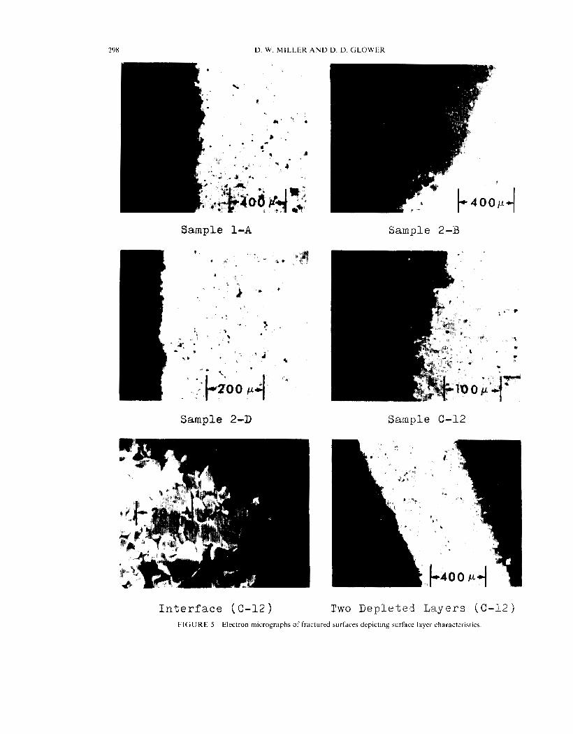
Interface ( C - 1 2 ) Two Depleted Layers ((2-12) FIGURE 5 Electron micrographs of fractured surfaces depictmy surface layer characteristics.
OXYGEN DEPLETED PZT SURFACE LAYERS 299
various positions on the surface of the depleted sample. The homogeneity of the surface layer was found to be 5 ':.b. The conductivity could only be determined after the mobility (discussed in the ensuing paragraphs) and the layer thickness were measured. The thicknesses were measured using electron micrographs of the fractured surfaces. Representative micrographs are shown in Figure 5. The oxygen defect concentration was determined using the nominal layer thickness and the measured weight loss. The conductivity. carrier concentration, defect concentration activation energy and nominal surface layer thickness for each sample are tabulated in Table I.
TABLE I Compilation ofdata from Samples I - A . 2-B and C-l?
Sample 1 - A 2-B c-l2
N here : p = 0.2 cm2 volt-sec. 7 = 300 K
The analysis of the properties reported in Table I utilized a partially ionized and partially compen- sated semiconductor model.I2 This model was chosen since the activation energy was large and since the carrier concentration is significantly lower than the defect concentration. The details of the model are discussed in Appendix B.
This model predicts that
AE = E, - E , = E, + kT In [-- N , 1. ( 2 ) f i ( N , - N A )
where E, is the donor energy level and N , is the compensation concentration. In comparing this result to the case where N , -+ 0 (uncompensated). which predicts that
kT 2
AE = E , - E, = E,f2 - - In
it can be concluded that
E,/2 < E, - E, < E,. (4)
Therefore the activation energy is a function ofthe degree of compensation and not the donor or defect concentration. This agrees with the data reported in Table I, where N , is approximately independent of both the carrier concentration and the activation energy. It can thus be concluded that the donor level energy is between 0.22 eV and 0.28 eV.
It is of interest to note that the donor level energy is more than an order of magnitude less than the approximate 3.0 'eV band gap energy of both ~ n r e d u c e d ' ~ - ' ~ and reduced16 perovskite materials. This indicates that the carrier concentration is entirely dependent upon the donor and compen- sation concentration, since the carrier concen- tration of the highly compensated p-type PZT is insignificant.
The Hall effect was used to determine the mobility and the semiconductor type. The experimental apparatus and geometry are shown in Figure 6. One should note that the usual Hall effect geo- metry" was not used in this measurement. The
1 l I V-:i:F;A 1 1 p VARIAN ASSOC.
SUPPLY GAUSSMETER
FIGURE 6 Block diagram oftheexperimcntal apparatus used for mobility measurements.
300 D. W . MILLER AND D. D. GLOWER
simplified geometry was employed in order to minimize the source resistance and maximize the sample current.
Since the Hall voltage source resistance was high and the mobility low there were measurement limitations due to thermal noise. However. with the geometry depicted in Figure 6 the signal to noise ratio was significantly increased although the width to length ratio was 0.639 and required correction in order to account for Hall field shorting from the end electrodes. These corrections factors are tabulated by Putley.18 Using the apparatus and geometry shown in Figure 6, the theoretical signal to noise ratio is 18 :l for a sample current of 1 lOnA and a magnetic field of4 kilogauss. The thermal noise plus the precision error intro- duced by the digital voltmeter predict a standard deviation of k0.074 cm2jvolt-sec. This compares favorably with the experimental statistical error of k0.12 cm2/volt-sec. Consequently, the measured Hall mobility is 0.2 0.12 cm2/volt-sec. Since the Hall coefficient is negative it can also be concluded that the semiconductor is n-type as indicated by thermoelectric probe measurements and reported by other investigators16* l 9 for reduced perovskites.
The dielectric properties of oxygen depleted PZT were investigated through the measurement of the capacitance and dissipation factor as a function of frequency. A General Radio 1615-A Capacitance Bridge, 1232-A R.F. Detector and a Wavetek 114 Function Generator were used for these measurements. The results are depicted in Figures 7 and S for sample 2-D which has a nominal 25 micron depleted surface layer and for a virgin PZT specimen.
These data were measured and analyzed with the objectives :
(1) to investigate changes in the dielectric properties of the oxygen depleted semi- conductor layer,
(2) to verify that the depletion process does not significantly perturb the dielectric properties of the PZT substrate.
The analysis of the data shown in Figures 7 and 8 was carried out using a simple two layer capacitance-resistance model which was suggested by Schlosser and Drougard" and is discussed in Appendix C . Using this model it can be shown that,
CTIo40 = c,, ( 5 )
and that,
c T l - c, w+a, 1 + C,/CF,
- (6)
where C, is the total capacitance of the oxygen depleted sample, C, is the capacitance of the ferro- electric substrate and C, is the capacitance of the semiconductor layer. Also from this model the dissipation factor for the depleted sample. D,. was Found to tit a function of the form,
DT(m) = DF(O) f do)* ( 7 )
where g ( ( . ) approaches zero as the frequency approaches infinity.
In Figures 7 and S the capacitance and dissi- pation factor of a virgin PZT sample are also shown. Since the virgin sample and the depleted sample are identical in dimensions and were cut
r ---I
'
l IO2 103 104 7 3
FREQUEUCY (HERTZ)
FIGURE 7 Capacitance of an oxygen depleted PZT sample and a virgin sample vs frequency.
IO* FRECUENCV (HERTZ)
103 I o4
FIGURE 8 Dissipation factor of an oxygn deplcted PZT sample and a virgin sample W frequency.
OXYGEN DEPLETED PZT SURFACE LAYERS 301
from the same bulk sample, a direct comparison can be made. From the capacitance data it can be shown that,
= 0.61.
where C,, is the capacitance of the virgin material. Comparing this result with Eq. (5) it can be concluded that the capacitance ofthe virgin material and the capacitance of the PZT substrate of the depleted sample are approximately equal. Also as a result of the empirical lit of the dissipation factor data to the function expressed in Eq. (7), it was found that for frequencies above 1 kHz the dissipation factor ofthe PZT substrate, D,, is lop2. This result is compared to the dissipation factor of the virgin sample which was found to be 1.70 x for frequencies above l kHz. Therefore it can be concluded that
D, N D,V(f> 1 kHz). (9)
These two results indicate that the dielectric properties of the substrate are not Significantly perturbed during oxygen depletion of the surface layer.
If it is now assumed that the capacitance of the substrate is equal to that measured for the virgin material, the capacitance of the semiconductor can be determined at high frequencies from Eq. (6). The measured data indicate that the capacitance of the depleted sample becomes approximately independent of frequency at frequencies greater than 1 kHz Using Eq. (6), where the capacitance of the semiconductor layer is,
L T (10)
and the nominal semiconductor layer thickness of 25 microns indicates a relative dielectric constant of approximately two orders of magnitude less than that found in virgin PZT. A dielectric constant of this magnitude in low resistivity PZT is not plausible and as a consequence the inadequacy of the two layer model for quantitative analysis is apparent. This conclusion is verified by noting the break frequencies in the dissipation factor and capacitance data. These data indicate a dielectric constant considerably higher than obtained from the simple two layer model. However, the two layer model does indicate that the dielectric constant in the reduced layer is less than that found in virgin PZT. A more realistic model
c ~ I , > l X H z = 1 - CJCF"'
requiring a distributed analysis of the surface layer would possibly yield more quantitative results.
From the dielectric data it can also be concluded that charging at the semiconductor-substrate inter- face is negligible since this would require a third distinct layer in the model to represent the capacitive effect of these surface states.
IV. SUMMARY AND CONCLUSION
It has been shown that an oxygen depleted ceramic PZTsurface layer havingsemiconducting properties can be grown without significantly perturbing the dielectric properties of the substrate. The properties of this surface layer were investigated using conductivity versus temperature data, Hall effect measurements, and dielectric dispersion data. The results of these measurements indicate that the donor energy level is between 0.22 eV and 0.28 eV, the mobility is 0.2 0.12 cm2/volt-sec., and the relative dielectric constant is less than that measured in virgin PZT. The measured conduc- tivities of the n-type semiconductor layer were
to (ohm-cm)-' as compared to a conductivity of less than lo-" (ohm-cm)-' found in the highly compensated p-type virgin PZT.'
ACKNOWLEDGEMENTS
This work was partially supported by the Engineer- ing Experiment Station at The Ohio State Univer- sity. The authors also wish to thank Mrs. Charles Poteet for her aid in preparing the samples.
APPENDIX
A. Sample Preparation
All samples were cut to the prescribed size using a diamond saw and lapped using 8iM p grit. The following procedure was used to clean and etch the samples before placing them in the depletion chamber :
(1) Polish all surfaces with 10 p AI,O, using no
(2) Rinse in succession with Methanol, tri-
(3) Dry in a clean air stream.
liquid.
chlorethylene, and Methanol.
302 D. W. MILLER AND D. D. GLOWER
(4) Soak for two minutes in phosphoric acid. (5) Quench with Methanol and rinse in distilled
(6) Dry in a clean air stream. (7) Soak for five minutes in hydrofluoric acid. (8) Dry in a clean air stream but do not quench.
water.
B. Partially Ionized und PartiallJ3 Cornpenscited Semiconductor
The semiconductor model is derived from Blake- morel2. In the development of this model the following assumptions were made :
(1) The donors energy levels are close enough together to assume monovalency.
( 2 ) The compensation energy levels are also assumed to be monovalent.
(3) The compensation sites are completely ionized.
(4) The donor site density is greater than the compensation concentration which in turn is greater than the carrier concentration.
(5) Donor and compensation sites may be located both within the grains and in the grain boundaries.
(6) E, > k7:
Using these assumptions the number of ionized donor sites is
where N, , is the ionized donor concentration, n is the carrier concentration, N , is the acceptor compensation concentration and N,, is the neutral donor concentration. The ionized donor concentra- tion is related to the total concentration by
E, = ( E , - E d ) + k T l n ['"">: N A ) ] . (14)
If the semiconductor were assumed to be un- compensated, then
n N NDi = 'V, - N,, . (15)
Assuming that
n N , (16)
and using (15) it can be shown that
where N , is the density of states in the conduction band.
It can be concluded from (14) and (17) that the Fermi energy level in a partially ionized semi- conductor must lie between E , - E,:2 and E, - E,.
C. Tww Layer Caprrcitunce Resistunce . 4 4 0 d c / ~ ~
The ferroelectric substrate and the depleted sur- face layer are represented by the two layer series- parallel resistance-capacitance model shown in Figure 9. In this model the two semiconductor
I l l l I
I I
FIGURE 9 Two layer modcl used for thc analysla ofdiclcctric data.
layers in the actual physical device are represented by one layer. In developing the model the following notation is used :
C, = the capacitance ofthe semiconductor layer. R , = l/G, = the resistance ofthe semiconductor
= the admittance of the semiconductor layer. C, = the capacitance of the ferroelectric sub-
layer.
strate.
OXYGEN DEPLETED PZT SURFACE LAYERS 303
R , = 1/G, = the resistance of the ferroelectric where
Y, = the admittance of the ferroelectric sub-
C , = the total capacitance of the depleted
substrate.
strate.
sample. REFERENCES
sample. I . R. Gerson and H. Jaffe. ’Electrical Conducticity in Lead G, = the total conductance of the depleted
Y, = the total admittance ofthe depleted sample. Titanate Zirconate Ceramics’. J . Ph,ys. C/?rv?. ~ o i i t h 24, 979 ( 1963).
From elementary circuit theory the total ad- mittance is
Alter some elementary algebraic manipulation the total capacitance and dissipation factors are respectively,
and
Since GFi’G, 4 1, it can be shown that the total capacitance at the low and high frequency limits is
CT(o-0 = CF (21 1 and
Using the detinition of the dissipation factor for the ferroelectric substrate,
and noting from the measured data that
D, can be reduced to the general form
W O ) ) = DdW) + d r o )
2. J. L. Moll and J , Tarui. ‘A New Solid State Mc~norq Register’. IEEE Trans. E/ectro,~ Devices ED-IO, 333 (1963).
3. R. Zuleeg and H. H . Weider. ‘The Effect of Ferroelectric Polarization on Transistor Parameters’. Soid Stutr Elec- tronics 9, 657 ( 1966).
4. P. M. Heyman and G . H . Heilmcyer. ‘.4 Ferroelectric Field Effect Device’. Proc. IEEE 54, 842 ( 1966).
5. S. S. Perlman and K. H. Ludwig. ‘An .4dapt1rz Thin Film Transistor’. IEEE Truns. Electron D e v m s ED-14, X16 ( 1967).
6. J. H. McCusker and S. S. Perlman. ‘Improved Fcrroclectr~c Field Effect Device’. IEEE Trcrnr. Ekrctrorl De\./c,er ED-IS, 18‘(1968).
7. H. L. Stadlcr. ‘F~lm Charging by Fcrroelcctrics‘. P m w , / / J I ~ \
sf the Syrnpositrrn on Ferrorlecfrics (Ed. by E. F. Weller) p. 250. Elsevier. New York (1967).
8. G. G . Teather and L. Young. ‘Nondestructitc Readout ol‘ Ferroelectrics by Field Effect Conductivity Modulation’. Solid Stute Electronics 11, 527 ( 1968).
9. J. C. Crawford and F. L. English. ‘Ccramic Ferroelectric Field Effect Studies’. IEEE Trans. Electron Drricrs ED 16, 525 (1969).
IO. J . C . Crawford. ‘Ferroclectric Field Effect Studies at Lob Temperatures’. Ferroelecfrrcr I , 23 (1970).
I l , C. E. Wicks and F. E. Black. Thermodymnlic Propwtw.\ of 65 Elements Their Or/des. Hulides Curh/c/e.r trnd N/fr ides U.S. Government Printing Office. Bulletin 605. U.S. Bureau of Mines. p. 42 (1963).
12. J. S. Blakemore. Semiconductor S1arf.yric.r. Chapter D Pergamon Press. Inc.. New York ( I Y h L ) .
13. L. C. Walters and R. E. Grace. ‘Formation of Point Defects in Strontium Titanate’. J , Chem. Solids 28. 239 (1967).
14. G. A. Cox. G. G . Roberts and R. H . Tredgold. ‘The Optical Absorption Edge of Barium Titanatc‘. Brit . J . Appl. P/IKS . 17, 743 ( 1966).
A . C. Conductivity and EMF Studies’. Ph.D. Dissertation (unpublished). The Ohio State University 1970).
16. D. E. Sawyer. ‘Photosensitive Barium Titanate Schottky Diodes’. Appl. Phys. Let1er.r 13, 392 ( 196X).
I ? . E. H. Putley. The Hall E j j k t cmd Relaird Phrnomrrlcr. pp. 154-155. Butterworth and Co.. Ltd.. London (1960).
18. E. H. Putley. The Hall Ef/ect and Rrlurrcl Phcnomcwrr. pp. 42--55.
19. H. W. Gandy. ’Optical Transmission of Heat Trzatcd Strontium Titanate’. Ph~,.r. Rev. 113, 795 11959).
20. H. Schlosser and M. E. Drougard. ‘Surface Laqcrs on Barium Titanate Single Crystals Above the Curic Point’. J . Appl. Phys. 32, 1227 1 1961 j.
15. J . G. Burt. ‘Defect Mechanism in Lead Zirconate Titanate