® WHITE PAPER The Role of Jitter in Timing Signals Timing signal jitter can have a profound impact on a wide variety of applications from analog radio frequency (RF) or audio-to-digital communications. While information in a communications system, for example, is extracted from serial data streams by sampling the data signal at specific points, the presence of small quantities of jitter can alter the edge positions enough to lead to data errors and high bit-error rates. Complicating the measurement of jitter is the way it is specified. Generally, timing signal jitter is specified in different ways from one application environment to another. For example, in digital data path synchronization applications, jitter is specified in the time domain as period or cycle-to-cycle jitter. In data communications applications, jitter is specified in the frequency domain as phase noise or “root mean square” (RMS) jitter. This paper provides a basic tutorial on timing signal jitter for designers building electronics systems. It defines this phenomenon and describes how it is measured in different applications. As part of that process, it explains the many ways timing jitter is specified and the differences between terms such as period jitter, cycle-to-cycle jitter and absolute period jitter. It then uses some common applications, such as the use of first-in/first-out (FIFO) memory devices in data acquisition subsystems, to describe the impact of jitter and basic error detection and recovery strategies. Defining jitter A timing signal is defined as a repetitive digital signal, as shown in figure 1. Typically, these signals are used to synchronize the transfer of data between two points, but their role varies widely from application to application. In digital chips, they are usually employed to sequence data through a set of processing stages in a pipeline. Analog applications, in contrast, may use a timing signal to sample a digital-to-analog converter (DAC) to digitize an audio signal. Communications systems designers use timing signals to synchronize the transmission of data over high-speed serial links, such as local area networks (LANs) and wide area networks (WANs). However, designers of RF systems use timing signals in the front end of their design to convert the modulated analog signal into the digital domain for digital signal processing (DSP). In each of these applications, the performance and reliability of the system can be dramatically affected by the quality of the timing signals used. IDT ® THE ROLE OF JITTER IN TIMING SIGNALS
Transcript
® white paper
The Role of Jitter in Timing Signals
Timing signal jitter can have a profound impact on a wide variety of applications from analog radio frequency (RF) or audio-to-digital communications. While information in a communications system, for example, is extracted from serial data streams by sampling the data signal at specific points, the presence of small quantities of jitter can alter the edge positions enough to lead to data errors and high bit-error rates. Complicating the measurement of jitter is the way it is specified. Generally, timing signal jitter is specified in different ways from one application environment to another. For example, in digital data path synchronization applications, jitter is specified in the time domain as period or cycle-to-cycle jitter. In data communications applications, jitter is specified in the frequency domain as phase noise or “root mean square” (RMS) jitter.
This paper provides a basic tutorial on timing signal jitter for designers building electronics systems. It defines this phenomenon and describes how it is measured in different applications. As part of that process, it explains the many ways timing jitter is specified and the differences between terms such as period jitter, cycle-to-cycle jitter and absolute period jitter. It then uses some common applications, such as the use of first-in/first-out (FIFO) memory devices in data acquisition subsystems, to describe the impact of jitter and basic error detection and recovery strategies.
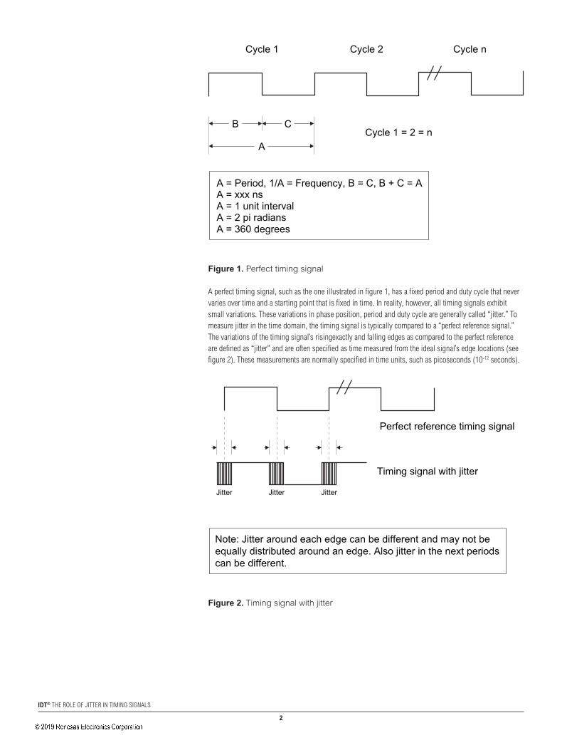
Defining jitterA timing signal is defined as a repetitive digital signal, as shown in figure 1. Typically, these signals are used to synchronize the transfer of data between two points, but their role varies widely from application to application. In digital chips, they are usually employed to sequence data through a set of processing stages in a pipeline. Analog applications, in contrast, may use a timing signal to sample a digital-to-analog converter (DAC) to digitize an audio signal. Communications systems designers use timing signals to synchronize the transmission of data over high-speed serial links, such as local area networks (LANs) and wide area networks (WANs). However, designers of RF systems use timing signals in the front end of their design to convert the modulated analog signal into the digital domain for digital signal processing (DSP). In each of these applications, the performance and reliability of the system can be dramatically affected by the quality of the timing signals used.
�
iDt® THe ROLe OF JITTeR IN TIMING SIGNALS
�
iDt® THe ROLe OF JITTeR IN TIMING SIGNALS
A = Period, 1/A = Frequency, B = C, B + C = AA = xxx nsA = 1 unit intervalA = 2 pi radiansA = 360 degrees
Cycle 1 = 2 = n
Cycle 1
B
A
C
Cycle 2 Cycle n
Figure 1. Perfect timing signal
Figure 1. Perfect timing signal
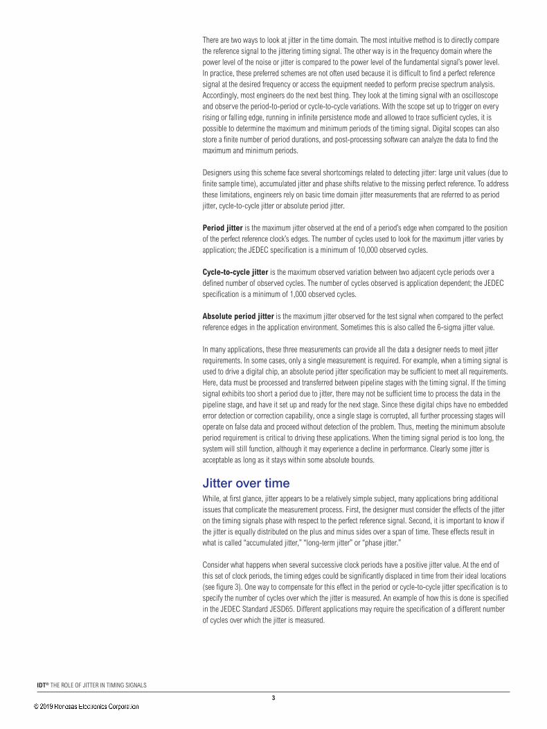
A perfect timing signal, such as the one illustrated in figure 1, has a fixed period and duty cycle that never varies over time and a starting point that is fixed in time. In reality, however, all timing signals exhibit small variations. These variations in phase position, period and duty cycle are generally called “jitter.” To measure jitter in the time domain, the timing signal is typically compared to a “perfect reference signal.” The variations of the timing signal’s risingexactly and falling edges as compared to the perfect reference are defined as “jitter” and are often specified as time measured from the ideal signal’s edge locations (see figure 2). These measurements are normally specified in time units, such as picoseconds (10-12 seconds).Figure 2. Timing signal with jitter
Perfect reference timing signal
Timing signal with jitter
JitterJitterJitter
Note: Jitter around each edge can be different and may not beequally distributed around an edge. Also jitter in the next periods can be different.
Figure 2. Timing signal with jitter
�
iDt® THe ROLe OF JITTeR IN TIMING SIGNALS
There are two ways to look at jitter in the time domain. The most intuitive method is to directly compare the reference signal to the jittering timing signal. The other way is in the frequency domain where the power level of the noise or jitter is compared to the power level of the fundamental signal’s power level. In practice, these preferred schemes are not often used because it is difficult to find a perfect reference signal at the desired frequency or access the equipment needed to perform precise spectrum analysis. Accordingly, most engineers do the next best thing. They look at the timing signal with an oscilloscope and observe the period-to-period or cycle-to-cycle variations. With the scope set up to trigger on every rising or falling edge, running in infinite persistence mode and allowed to trace sufficient cycles, it is possible to determine the maximum and minimum periods of the timing signal. Digital scopes can also store a finite number of period durations, and post-processing software can analyze the data to find the maximum and minimum periods.
Designers using this scheme face several shortcomings related to detecting jitter: large unit values (due to finite sample time), accumulated jitter and phase shifts relative to the missing perfect reference. To address these limitations, engineers rely on basic time domain jitter measurements that are referred to as period jitter, cycle-to-cycle jitter or absolute period jitter.
period jitter is the maximum jitter observed at the end of a period’s edge when compared to the position of the perfect reference clock’s edges. The number of cycles used to look for the maximum jitter varies by application; the JeDeC specification is a minimum of 10,000 observed cycles.
Cycle-to-cycle jitter is the maximum observed variation between two adjacent cycle periods over a defined number of observed cycles. The number of cycles observed is application dependent; the JeDeC specification is a minimum of 1,000 observed cycles.
absolute period jitter is the maximum jitter observed for the test signal when compared to the perfect reference edges in the application environment. Sometimes this is also called the 6-sigma jitter value.
In many applications, these three measurements can provide all the data a designer needs to meet jitter requirements. In some cases, only a single measurement is required. For example, when a timing signal is used to drive a digital chip, an absolute period jitter specification may be sufficient to meet all requirements. Here, data must be processed and transferred between pipeline stages with the timing signal. If the timing signal exhibits too short a period due to jitter, there may not be sufficient time to process the data in the pipeline stage, and have it set up and ready for the next stage. Since these digital chips have no embedded error detection or correction capability, once a single stage is corrupted, all further processing stages will operate on false data and proceed without detection of the problem. Thus, meeting the minimum absolute period requirement is critical to driving these applications. When the timing signal period is too long, the system will still function, although it may experience a decline in performance. Clearly some jitter is acceptable as long as it stays within some absolute bounds.
Jitter over timeWhile, at first glance, jitter appears to be a relatively simple subject, many applications bring additional issues that complicate the measurement process. First, the designer must consider the effects of the jitter on the timing signals phase with respect to the perfect reference signal. Second, it is important to know if the jitter is equally distributed on the plus and minus sides over a span of time. These effects result in what is called “accumulated jitter,” “long-term jitter” or “phase jitter.”
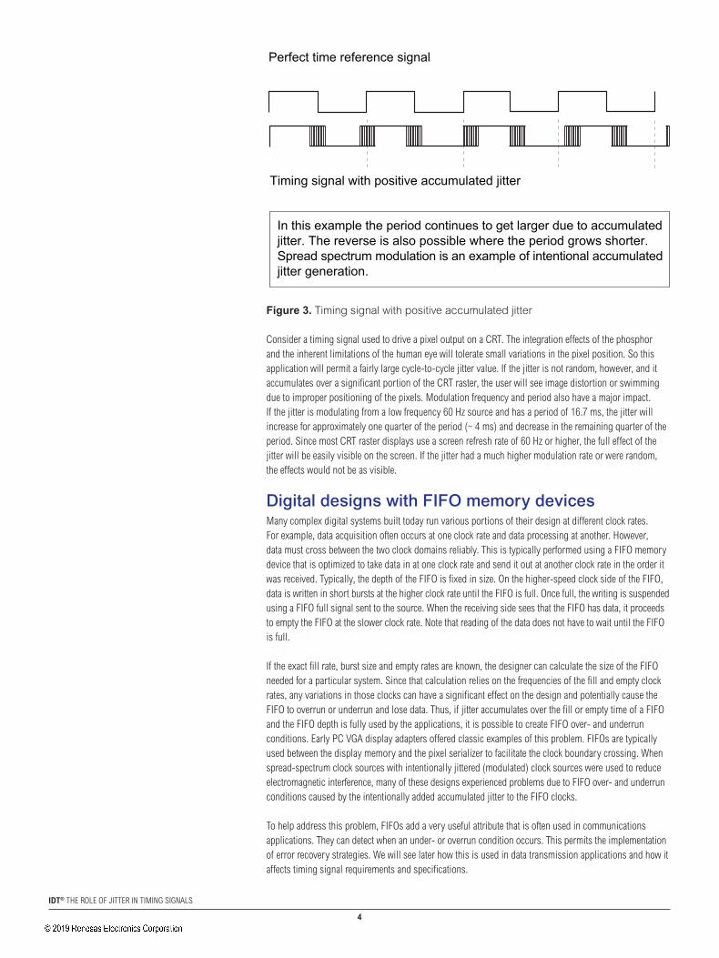
Consider what happens when several successive clock periods have a positive jitter value. At the end of this set of clock periods, the timing edges could be significantly displaced in time from their ideal locations (see figure 3). One way to compensate for this effect in the period or cycle-to-cycle jitter specification is to specify the number of cycles over which the jitter is measured. An example of how this is done is specified in the JeDeC Standard JeSD65. Different applications may require the specification of a different number of cycles over which the jitter is measured.
�
iDt® THe ROLe OF JITTeR IN TIMING SIGNALS
Figure 3. Timing signal with accumulated jitter
Perfect time reference signal
Timing signal with positive accumulated jitter
In this example the period continues to get larger due to accumulated jitter. The reverse is also possible where the period grows shorter.Spread spectrum modulation is an example of intentional accumulatedjitter generation.
Figure 3. Timing signal with positive accumulated jitter
Consider a timing signal used to drive a pixel output on a CRT. The integration effects of the phosphor and the inherent limitations of the human eye will tolerate small variations in the pixel position. So this application will permit a fairly large cycle-to-cycle jitter value. If the jitter is not random, however, and it accumulates over a significant portion of the CRT raster, the user will see image distortion or swimming due to improper positioning of the pixels. Modulation frequency and period also have a major impact. If the jitter is modulating from a low frequency 60 Hz source and has a period of 16.7 ms, the jitter will increase for approximately one quarter of the period (~ 4 ms) and decrease in the remaining quarter of the period. Since most CRT raster displays use a screen refresh rate of 60 Hz or higher, the full effect of the jitter will be easily visible on the screen. If the jitter had a much higher modulation rate or were random, the effects would not be as visible.
Digital designs with FIFO memory devicesMany complex digital systems built today run various portions of their design at different clock rates. For example, data acquisition often occurs at one clock rate and data processing at another. However, data must cross between the two clock domains reliably. This is typically performed using a FIFO memory device that is optimized to take data in at one clock rate and send it out at another clock rate in the order it was received. Typically, the depth of the FIFO is fixed in size. On the higher-speed clock side of the FIFO, data is written in short bursts at the higher clock rate until the FIFO is full. Once full, the writing is suspended using a FIFO full signal sent to the source. When the receiving side sees that the FIFO has data, it proceeds to empty the FIFO at the slower clock rate. Note that reading of the data does not have to wait until the FIFO is full.
If the exact fill rate, burst size and empty rates are known, the designer can calculate the size of the FIFO needed for a particular system. Since that calculation relies on the frequencies of the fill and empty clock rates, any variations in those clocks can have a significant effect on the design and potentially cause the FIFO to overrun or underrun and lose data. Thus, if jitter accumulates over the fill or empty time of a FIFO and the FIFO depth is fully used by the applications, it is possible to create FIFO over- and underrun conditions. early PC VGA display adapters offered classic examples of this problem. FIFOs are typically used between the display memory and the pixel serializer to facilitate the clock boundary crossing. When spread-spectrum clock sources with intentionally jittered (modulated) clock sources were used to reduce electromagnetic interference, many of these designs experienced problems due to FIFO over- and underrun conditions caused by the intentionally added accumulated jitter to the FIFO clocks.
To help address this problem, FIFOs add a very useful attribute that is often used in communications applications. They can detect when an under- or overrun condition occurs. This permits the implementation of error recovery strategies. We will see later how this is used in data transmission applications and how it affects timing signal requirements and specifications.
�
iDt® THe ROLe OF JITTeR IN TIMING SIGNALS
ADC/DAC sampling clocksConversion of analog signals to the digital domain and back are highly dependent on the quality of the data conversion timing signal clock. Today, due to advances in DSP technology, most signal processing is performed in the digital domain. This includes functions such as echo canceling, cross-talk reduction, and equalization for signal restoration, modulation and demodulation. All of these digital processing functions are highly dependent on the quality of the “frontend” data conversion. In turn, the quality of the data conversion is directly related to the quality of the sampling clock signal. Many modulation/demodulation schemes for data transmission over copper or RF use a combination of frequency modulation, phase modulation and amplitude modulation. These complex schemes are used to improve data transfer efficiency. Therefore, if the sampled data stream is using all of these modulation schemes, and the sampling clock has jitter in phase and frequency, the sampling clock can actually add its own phase and frequency modulation to the digital data, making it more difficult for the DSP to process the converted digital data properly and extract the correct data. If the sampling clock accumulates jitter over a “symbol” time, it will begin to sample the next symbol too early or late and create a problem called intersymbol interference.
Data transmission clockingWhile the topic of the transmission of digital data over long distances and the impact of jitter on that transmission is admittedly extremely complex, the following discussion offers a simplified explanation of the basic issues involved. Most data transmission schemes use an encoding scheme to embed the clock in the serial data stream so that it can be recovered at the receiving end and used to sample the clock/data stream, recovering the data-only portion. Most receivers have a function called a clock data recovery (CDR) block. This block is typically a phase locked loop (PLL) or delay locked loop (DLL) that requires sufficient edges in the data stream to lock to the stream and generate the embedded clock. Systems use any of several schemes to ensure that sufficient edges in the clock data stream are available. For example, when long streams of 0s or 1s are encountered, bits of the opposite polarity are inserted using an agreed-upon set of rules understood by the transmitter and receiver. A commonly used scheme is to convert an 8-bit block of data to a 10-bit block of data. The mapping of the 8-bit codes to the 10-bit codes is such that only 10-bit codes with the highest number of bit transitions are used. The transmitter and receiver must know the mapping table. While this scheme adds overhead to the data stream, it ensures reliable clock recovery.
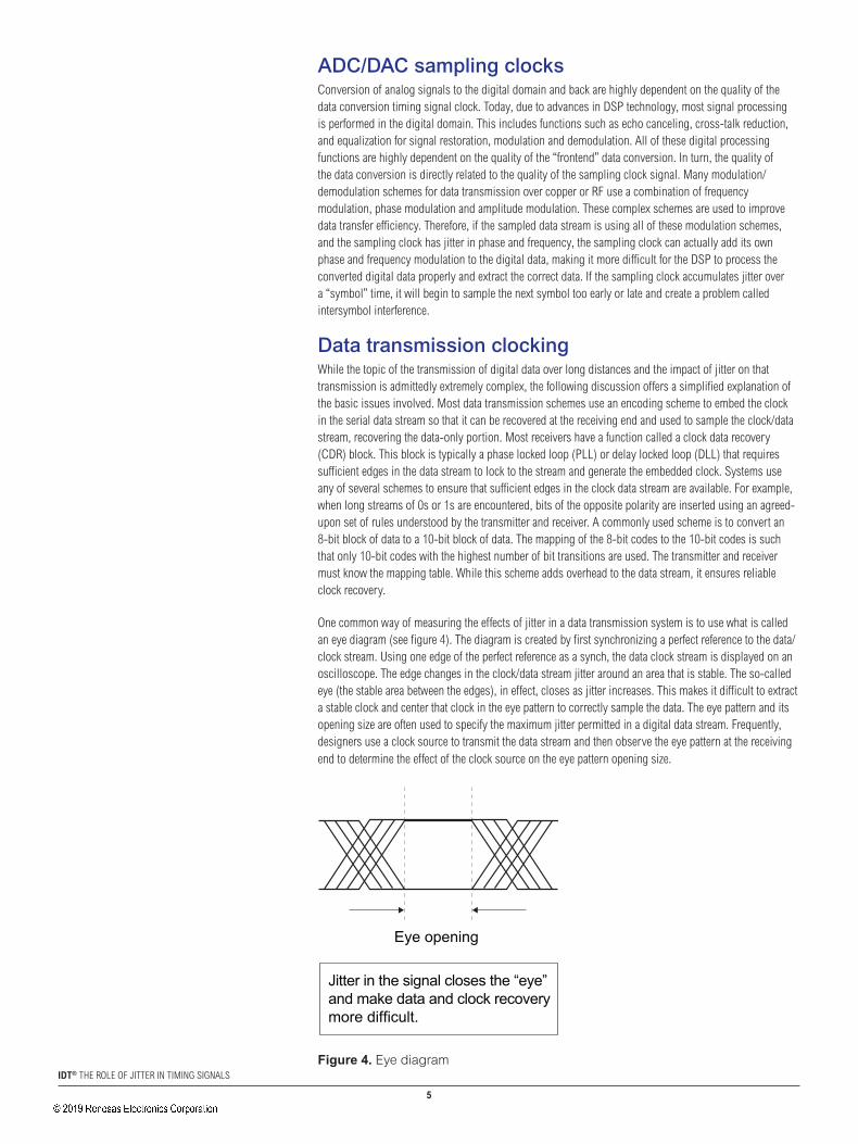
One common way of measuring the effects of jitter in a data transmission system is to use what is called an eye diagram (see figure 4). The diagram is created by first synchronizing a perfect reference to the data/clock stream. Using one edge of the perfect reference as a synch, the data clock stream is displayed on an oscilloscope. The edge changes in the clock/data stream jitter around an area that is stable. The so-called eye (the stable area between the edges), in effect, closes as jitter increases. This makes it difficult to extract a stable clock and center that clock in the eye pattern to correctly sample the data. The eye pattern and its opening size are often used to specify the maximum jitter permitted in a digital data stream. Frequently, designers use a clock source to transmit the data stream and then observe the eye pattern at the receiving end to determine the effect of the clock source on the eye pattern opening size.Figure 4. Eye diagrams
Eye opening
Jitter in the signal closes the “eye”and make data and clock recoverymore difficult.
Figure 4. Eye diagram
�
iDt® THe ROLe OF JITTeR IN TIMING SIGNALS
Tolerating errorsData transmission schemes make one very important assumption not present in many other clocking applications: they assume transmission errors will occur. Signal degradation and noise (jitter) will cause errors. Furthermore, while it may be possible to build an error-free environment, it may not be economically feasible. Therefore, in many system designs, errors are often tolerated to keep costs low.
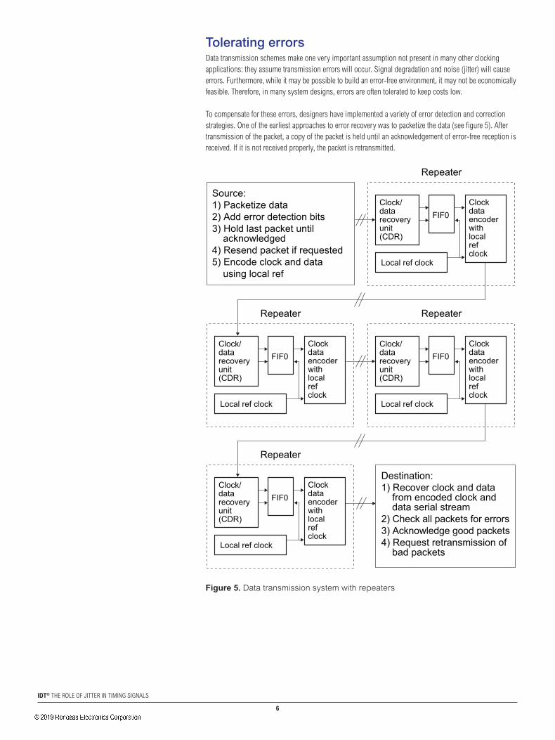
To compensate for these errors, designers have implemented a variety of error detection and correction strategies. One of the earliest approaches to error recovery was to packetize the data (see figure 5). After transmission of the packet, a copy of the packet is held until an acknowledgement of error-free reception is received. If it is not received properly, the packet is retransmitted.Figure 5. Data transmission system with repeaters
Source:1) Packetize data2) Add error detection bits3) Hold last packet until acknowledged4) Resend packet if requested5) Encode clock and data using local ref
Destination:1) Recover clock and data from encoded clock and data serial stream2) Check all packets for errors3) Acknowledge good packets4) Request retransmission of bad packets
Repeater
Clock/datarecoveryunit (CDR)
Clockdataencoderwithlocalrefclock
FIF0
Local ref clock
Repeater
Clock/datarecoveryunit (CDR)
Clockdataencoderwithlocalrefclock
FIF0
Local ref clock
Repeater
Clock/datarecoveryunit (CDR)
Clockdataencoderwithlocalrefclock
FIF0
Local ref clock
Repeater
Clock/datarecoveryunit (CDR)
Clockdataencoderwithlocalrefclock
FIF0
Local ref clock
Figure 5. Data transmission system with repeaters
�
iDt® THe ROLe OF JITTeR IN TIMING SIGNALS
The packet approach is used for a number of reasons. The most basic is that if a packet is lost, it is relatively easy to detect this and retransmit. This is accomplished by adding overhead to the packet, such as a packet sequence number, an address for routing and an error-detection code. In addition, each packet’s boundaries must be detectable. This is usually accomplished by beginning the packet with what is called a code violation. This is a blatant violation of the clock/data encoding scheme rules that is easily detected. For example, in an 8/10 encoding scheme, picking a 10-bit value that is not a valid 8-bit mapping can be used to create a code violation and detect the beginning of the packet. The end of the packet can be determined by another code violation, an agreed fixed length of the packet or a packet-length field in the packet’s header.
In reality, each segment of the transmission system is a different clock domain, where the difference might be slight but can have a profound effect on performance. This problem is very similar to the FIFO clock domain-crossing issues in complex digital designs discussed earlier. In transmission systems, the FIFO is often called an “elasticity buffer.” If the two segments have a fixed offset in clock frequency, the elasticity buffer cannot prevent over- or underrun conditions; eventually they will occur. But a buffer can reduce the frequency of the errors at the expense of some data delay. Moreover, since FIFOs can detect the error, the system can request retransmission of the packet with the error. The packet approach also allows for the implementation of another strategy to deal with the clocking issues over transmission systems. By inserting a variable small gap between packets, clocks that do not carry data can be inserted and extracted to adjust to the differences in clock frequencies between transmission segments.
When one considers all of the issues described above, including accepting certain levels of error rates, error recovery strategies, packet size, packet gap size, number of retimed segments and clocking sources, the simple specification of period or cycle-to-cycle jitter may not provide an acceptable cost or performance solution. For example, any large jitter event that occurs infrequently is perfectly acceptable if the designer implements a robust error-recovery strategy for infrequent errors.
While accumulated jitter over a packet length would introduce a potential error in every packet, the cycle-to-cycle jitter could be very small. But if jitter is accumulated over the packet’s time interval sufficiently to cause a bit error in the packet, it could become an issue. Clearly, designers need to specify jitter differently for these types of applications. Later we will see how specifying jitter as RMS power and in the frequency domain as phase noise is more applicable for these applications.
�
iDt® THe ROLe OF JITTeR IN TIMING SIGNALS
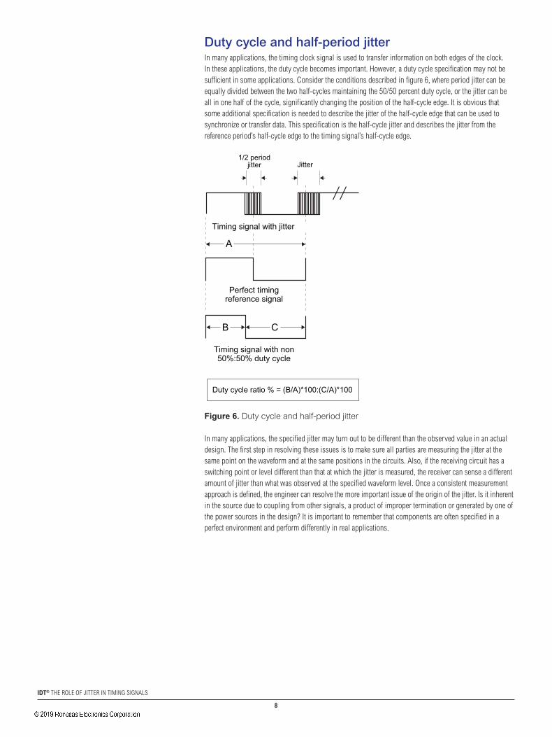
Duty cycle and half-period jitterIn many applications, the timing clock signal is used to transfer information on both edges of the clock. In these applications, the duty cycle becomes important. However, a duty cycle specification may not be sufficient in some applications. Consider the conditions described in figure 6, where period jitter can be equally divided between the two half-cycles maintaining the 50/50 percent duty cycle, or the jitter can be all in one half of the cycle, significantly changing the position of the half-cycle edge. It is obvious that some additional specification is needed to describe the jitter of the half-cycle edge that can be used to synchronize or transfer data. This specification is the half-cycle jitter and describes the jitter from the reference period’s half-cycle edge to the timing signal’s half-cycle edge.Figure 6. Duty cycle and
half-period jitter
Timing signal with jitter
Perfect timingreference signal
Timing signal with non50%:50% duty cycle
A
B C
Jitter1/2 period
jitter
Duty cycle ratio % = (B/A)*100:(C/A)*100
Figure 6. Duty cycle and half-period jitter
In many applications, the specified jitter may turn out to be different than the observed value in an actual design. The first step in resolving these issues is to make sure all parties are measuring the jitter at the same point on the waveform and at the same positions in the circuits. Also, if the receiving circuit has a switching point or level different than that at which the jitter is measured, the receiver can sense a different amount of jitter than what was observed at the specified waveform level. Once a consistent measurement approach is defined, the engineer can resolve the more important issue of the origin of the jitter. Is it inherent in the source due to coupling from other signals, a product of improper termination or generated by one of the power sources in the design? It is important to remember that components are often specified in a perfect environment and perform differently in real applications.
�
iDt® THe ROLe OF JITTeR IN TIMING SIGNALS
Units of measurementJitter is typically measured and specified in picoseconds from some reference edge and over some number of specified cycles. However, other units of measure can be used as well. One method is to express the jitter as a percentage of the reference period. In many applications, the reference period is call a unit interval (UI), and the jitter is specified as a ratio or percentage of the UI. Other measurements used are degrees where 1 UI = 360 degrees = 1 period = 2 pi radians.
A good way to understand the conversion is to use an example. Consider the OC-3 clock frequency of 155.52 MHz with +/-50 ps of jitter or a total jitter of 100 ps.
One period = 1/155.52 MHZ = 1 UI = 6.43 ns = 6430 ps = 360 degrees = 2 x 3.1418 radians
Jitter as ps =100 ps
Jitter as ratio of UI = 100 ps/6430 ps = 0.01555 UI
Jitter as % UI = 100 ps/6430 ps = 0.01555 UI = 0.01555 UI x 100 = 1.555% UI
Jitter as degrees = 100 ps/6430 ps x 360 degrees = 5.598 degrees of jitter
Jitter as radians = 100 ps/6430 ps x 2 x 3.1418 radians = 0.0977 radians of jitter
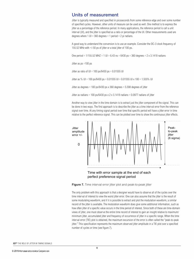
Another way to view jitter in the time domain is to extract just the jitter component of the signal. This can be done in two ways. The first approach is to describe the jitter as a time interval error from the reference signal over time. At any timing signal period over time that specific period will have a jitter error in time relative to the perfect reference signal. This can be plotted over time to show the continuous jitter effects.
Time with error sample at the end of eachperfect preference signal period
Jitteramplitudeerror +/-
Peak-to-peakjitter(6 sigma)
0
Figure 7. Time interval error jitter plot and peak-to-peak jitter
Figure 7. Time interval error jitter plot and peak-to-peak jitter
The only problem with this approach is that a designer would have to observe all of the cycles over the time interval of interest to view the worst jitter error. One can also assume that the jitter is the result of some modulating waveform, and if it is possible to extract and plot the modulation waveform, a similar record of the jitter is available. The modulation waveform does give some additional information, such as how often jitter of a specific value occurs in the time period of interest. Since both of these are time-domain views of jitter, one must observe the entire time record of interest to gain an insight relative to maximum/minimum jitter, accumulated jitter and frequency of occurrence of jitter in a specific range. When the time interval error (TIe) plot is obtained, the maximum excursion of the error is often called the “peak-to-peak jitter.” This specification represents the maximum observed jitter amplitude in a TIe plot over a specified number of cycles or time (see figure 7).
�0
iDt® THe ROLe OF JITTeR IN TIMING SIGNALS
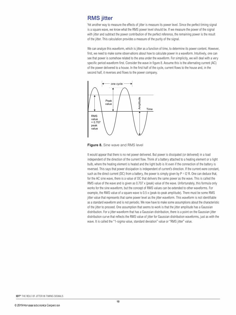
RMS jitterYet another way to measure the effects of jitter is measure its power level. Since the perfect timing signal is a square wave, we know what the RMS power level should be. If we measure the power of the signal with jitter and subtract the power contribution of the perfect reference, the remaining power is the result of the jitter. This calculation provides a measure of the purity of the signal.
We can analyze this waveform, which is jitter as a function of time, to determine its power content. However, first, we need to make some observations about how to calculate power in a waveform. Intuitively, one can see that power is somehow related to the area under the waveform. For simplicity, we will deal with a very specific period waveform first. Consider the wave in figure 8. Assume this is the alternating current (AC) of the power delivered to a house. In the first half of the cycle, current flows to the house and, in the second half, it reverses and flows to the power company.Figure 8. Sine wave and RMS level
RMSvalue= 0.707peakvalue
TimeAm
plitu
de
Peakvalue
one cycle
Figure 8. Sine wave and RMS level
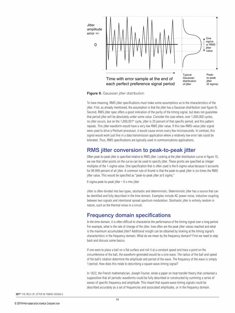
It would appear that there is no net power delivered. But power is dissipated (or delivered) in a load independent of the direction of the current flow. Think of a battery attached to a heating element or a light bulb, where the heating element is heated and the light bulb is lit even if the connection of the battery is reversed. This says that power dissipation is independent of current’s direction. If the current were constant, such as the direct current (DC) from a battery, the power is simply given by P = I2 R. One can deduce that, for the AC sine wave, there is a value of DC that delivers the same power as the wave. This is called the RMS value of the wave and is given as 0.707 x (peak) value of the wave. Unfortunately, this formula only works for the sine waveform, but the concept of RMS values can be extended to other waveforms. For example, the RMS value of a square wave is 0.5 x (peak-to-peak amplitude). There must be some RMS jitter value that represents that same power level as the jitter waveform. This waveform is not identifiable as a standard waveform and is not periodic. We now have to make some assumptions about the characteristic of the jitter to proceed. One assumption that seems to work is that the jitter amplitude has a Gaussian distribution. For a jitter waveform that has a Gaussian distribution, there is a point on the Gaussian jitter distribution curve that reflects the RMS value of jitter for Gaussian distribution waveforms, just as with the wave. It is called the “1-sigma value, standard deviation” value or “RMS jitter” value.
��
iDt® THe ROLe OF JITTeR IN TIMING SIGNALS
Time with error sample at the end ofeach perfect preference signal period
Jitteramplitudeerror +/-
Peak-to-peakjitter(6 sigma)
TypicalGaussiandistributionof jitter
Onesigmaor RMSjittervalue
0
Figure 9. Gaussian jitter distribution
Figure 9. Gaussian jitter distribution
To have meaning, RMS jitter specifications must make some assumptions as to the characteristics of the jitter. First, as already mentioned, the assumption is that the jitter has a Gaussian distribution (see figure 9). Second, RMS jitter spec offers a good indication of the purity of the timing signal, but does not guarantee that period jitter will be absolutely under some value. Consider the case where, over 1,000,000 cycles, no jitter occurs, but on the 1,000,001th cycle, jitter is 20 percent of that specific period, and this pattern repeats. This jitter waveform would have a very low RMS jitter value. If this low-RMS-value jitter signal were used to drive a Pentium processor, it would cause errors every few microseconds. In contrast, this signal would work just fine in a data transmission application where a relatively low error rate could be tolerated. Thus, RMS specifications are typically used in communications applications.
RMS jitter conversion to peak-to-peak jitterOften peak-to-peak jitter is specified relative to RMS jitter. Looking at the jitter distribution curve in figure 10, we see that other points on the curve can be used to specify jitter. These points are specified as integer multiples of the 1-sigma value. One specification that is often used is the 6-sigma value because it accounts for 99.999 percent of all jitter. A common rule of thumb is that the peak-to-peak jitter is six times the RMS jitter value. This would be specified as “peak-to-peak jitter at 6 sigma.”
6 sigma peak-to-peak jitter = 6 x rms jitter
Jitter is often divided into two types, stochastic and deterministic. Deterministic jitter has a source that can be identified and fully described in the time domain. examples include AC power noise, inductive coupling between two signals and intentional spread spectrum modulation. Stochastic jitter is entirely random in nature, such as the thermal noise in a circuit.
Frequency domain specificationsIn the time domain, it is often difficult to characterize the performance of the timing signal over a long period. For example, what is the rate of change of the jitter, how often are the peak jitter values reached and what is the maximum accumulated jitter? Additional insight can be obtained by looking at the timing signal’s characteristics in the frequency domain. What do we mean by the frequency domain? First we need to step back and discuss some basics.
If one were to place a ball on a flat surface and roll it at a constant speed and trace a point on the circumference of the ball, the waveform generated would be a sine wave. The radius of the ball and speed of the ball’s rotation determine the amplitude and period of the wave. The frequency of the wave is simply 1/period. How does this relate to describing a square wave-timing signal?
In 1822, the French mathematician, Joseph Fourier, wrote a paper on heat transfer theory that contained a supposition that all periodic waveforms could be fully described or constructed by summing a series of waves of specific frequency and amplitude. This meant that square wave-timing signals could be described accurately as a set of frequencies and associated amplitudes, or in the frequency domain.
��
iDt® THe ROLe OF JITTeR IN TIMING SIGNALS
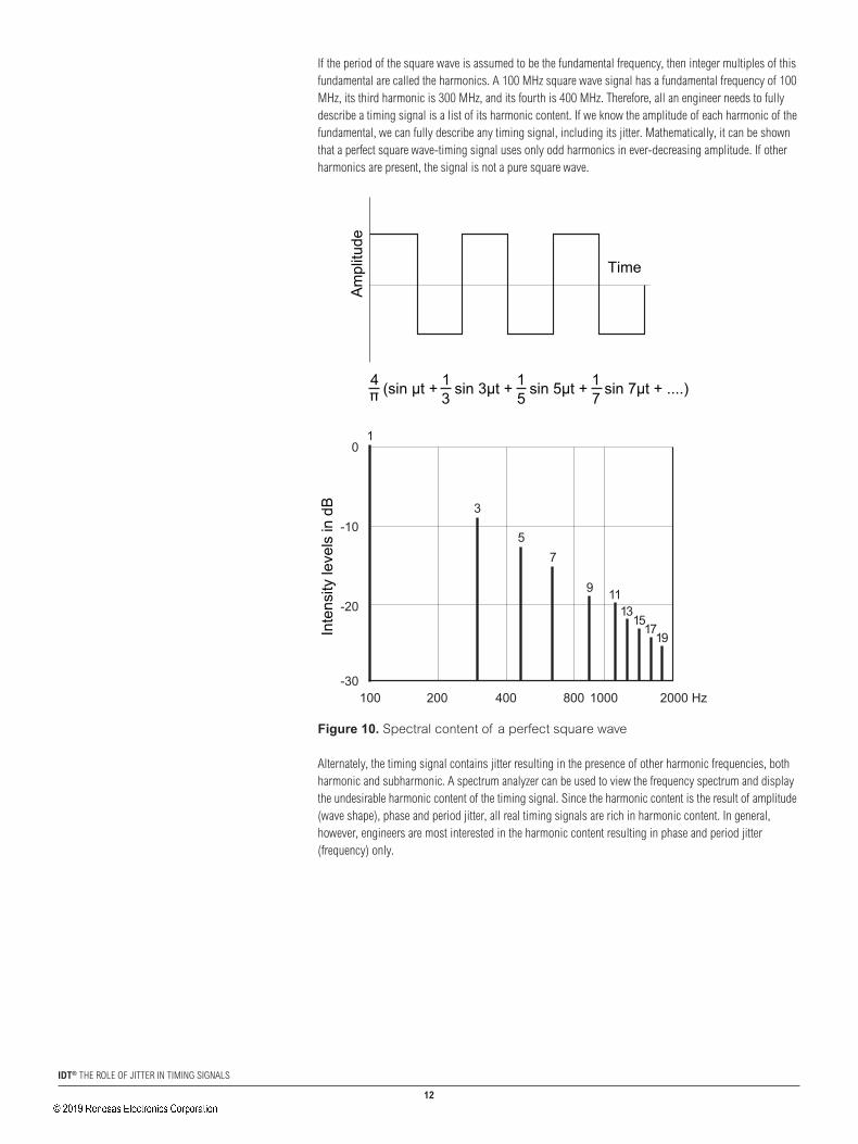
If the period of the square wave is assumed to be the fundamental frequency, then integer multiples of this fundamental are called the harmonics. A 100 MHz square wave signal has a fundamental frequency of 100 MHz, its third harmonic is 300 MHz, and its fourth is 400 MHz. Therefore, all an engineer needs to fully describe a timing signal is a list of its harmonic content. If we know the amplitude of each harmonic of the fundamental, we can fully describe any timing signal, including its jitter. Mathematically, it can be shown that a perfect square wave-timing signal uses only odd harmonics in ever-decreasing amplitude. If other harmonics are present, the signal is not a pure square wave.
Figure 11. Spectral content of a realistic timing signal
(Harmonics)
Due toJitter
A real square wave contains primarily odd harmonics content,but will also contain small amounts of even harmonic content.
Note that the harmonics are not pure and have bands of “noise jitter” around reach harmonics
We are primarily interested in the jitter around the first or fundamental since the zero crossings of the fundamental represents the jitter of the square wave period.
1 2 3 4 5 6 7 8
Figure 10. Spectral content of a perfect square wave
Am
plitu
de
Inte
nsity
leve
ls in
dB
Time
100
01
-10
-20
-30200 400
3
5
7
911
1315
1719
800 1000 2000 Hz
4 (sin µt +
1 sin 3µt +
1 sin 5µt +
1 sin 7µt + ....)3 5 7
Figure 10. Spectral content of a perfect square wave
Alternately, the timing signal contains jitter resulting in the presence of other harmonic frequencies, both harmonic and subharmonic. A spectrum analyzer can be used to view the frequency spectrum and display the undesirable harmonic content of the timing signal. Since the harmonic content is the result of amplitude (wave shape), phase and period jitter, all real timing signals are rich in harmonic content. In general, however, engineers are most interested in the harmonic content resulting in phase and period jitter (frequency) only.
��
iDt® THe ROLe OF JITTeR IN TIMING SIGNALS
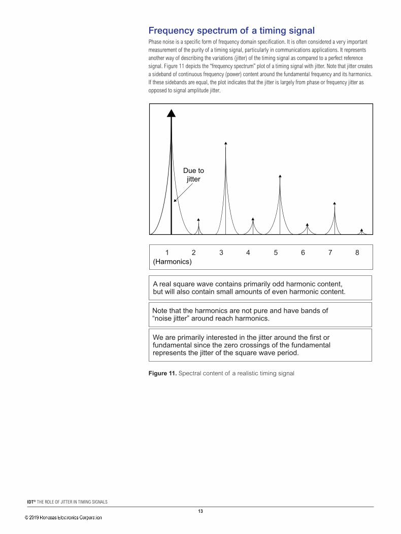
Frequency spectrum of a timing signalPhase noise is a specific form of frequency domain specification. It is often considered a very important measurement of the purity of a timing signal, particularly in communications applications. It represents another way of describing the variations (jitter) of the timing signal as compared to a perfect reference signal. Figure 11 depicts the “frequency spectrum” plot of a timing signal with jitter. Note that jitter creates a sideband of continuous frequency (power) content around the fundamental frequency and its harmonics. If these sidebands are equal, the plot indicates that the jitter is largely from phase or frequency jitter as opposed to signal amplitude jitter.Figure 11. Spectral content of a realistic timing signal
(Harmonics)
Due tojitter
A real square wave contains primarily odd harmonic content,but will also contain small amounts of even harmonic content.
Note that the harmonics are not pure and have bands of “noise jitter” around reach harmonics.
We are primarily interested in the jitter around the first or fundamental since the zero crossings of the fundamental represents the jitter of the square wave period.
1 2 3 4 5 6 7 8
Figure 11. Spectral content of a realistic timing signal
��
iDt® THe ROLe OF JITTeR IN TIMING SIGNALS
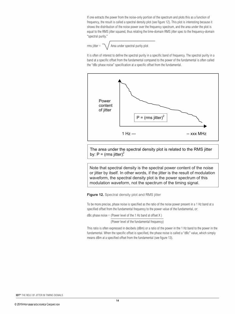
If one extracts the power from the noise-only portion of the spectrum and plots this as a function of frequency, the result is called a spectral density plot (see figure 12). This plot is interesting because it shows the distribution of the noise power over the frequency spectrum, and the area under the plot is equal to the RMS jitter squared, thus relating the time-domain RMS jitter spec to the frequency-domain “spectral purity.”
rms jitter = Area under spectral purity plot
It is often of interest to define the spectral purity in a specific band of frequency. The spectral purity in a band at a specific offset from the fundamental compared to the power of the fundamental is often called the “dBc phase noise” specification at a specific offset from the fundamental. Figure 12. Spectral density plot and RMS jitter
The area under the spectral density plot is related to the RMS jitterby: P = (rms jitter)2
1 Hz --- -- xxx MHz
Powercontentof jitter
P = (rms jitter)2
Note that spectral density is the spectral power content of the noise or jitter by itself. In other words, if the jitter is the result of modulation waveform, the spectral density plot is the power spectrum of this modulation waveform, not the spectrum of the timing signal.
.
Figure 12. Spectral density plot and RMS jitter
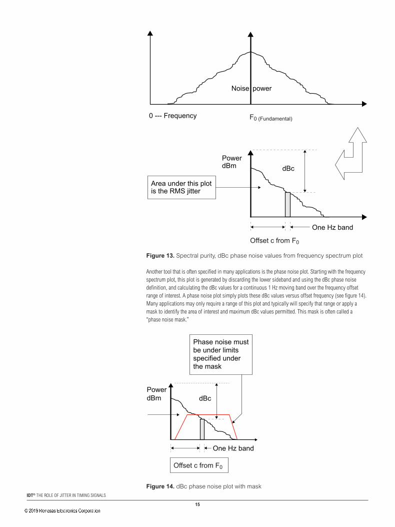
To be more precise, phase noise is specified as the ratio of the noise power present in a 1 Hz band at a specified offset from the fundamental frequency to the power value of the fundamental, or:
dBc phase noise = (Power level of the 1 Hz band at offset X )
(Power level of the fundamental frequency)
This ratio is often expressed in decibels (dBm) or a ratio of the power in the 1 Hz band to the power in the fundamental. When the specific offset is specified, the phase noise is called a “dBc” value, which simply means dBm at a specified offset from the fundamental (see figure 13).
��
iDt® THe ROLe OF JITTeR IN TIMING SIGNALS
PowerdBm
One Hz band
dBc
Offset c from F0
Figure 13. Spectral purity, dBc phase noise values from frequency spectrum plot
0 --- Frequency
Noise power
Area under this plotis the RMS jitter
F0 (Fundamental)
Figure 13. Spectral purity, dBc phase noise values from frequency spectrum plot
Another tool that is often specified in many applications is the phase noise plot. Starting with the frequency spectrum plot, this plot is generated by discarding the lower sideband and using the dBc phase noise definition, and calculating the dBc values for a continuous 1 Hz moving band over the frequency offset range of interest. A phase noise plot simply plots these dBc values versus offset frequency (see figure 14). Many applications may only require a range of this plot and typically will specify that range or apply a mask to identify the area of interest and maximum dBc values permitted. This mask is often called a “phase noise mask.”
Figure 14. dBc phase noise plot with mask
PowerdBm
One Hz band
dBc
Phase noise mustbe under limitsspecified underthe mask
Offset c from F0
Figure 14. dBc phase noise plot with mask
��
iDt® THe ROLe OF JITTeR IN TIMING SIGNALS
Phase noise measurement issuesAs with most timing specifications, measurements of phase noise are impacted by a number of factors. The primary issue relates to the capabilities of the equipment. Often the noise floor of the equipment is higher than the level of noise at large offsets. One way to determine the noise floor is to look at the flat part of the plot at very large offsets. This typically represents the noise floor. Also, as offsets decline in size, the quality of the local reference used in the equipment makes accurate measurements difficult. Again, the shape of the plot near the fundamental (small offsets) with a perfect source (equipment reference) will limit the detection of jitter.
ConclusionsGiven the wide range of topics covered in this paper, it is clear that the specification of timing jitter is highly complex. Many of the descriptions used here have been greatly simplified to meet space limitations. Those interested in investigating specific aspects of this discussion in more depth should start with the references listed below.
Obviously, the impact of timing signal jitter on a system can vary widely from one application to another. In some cases, it is more advantageous to measure and specify this phenomenon in the timing domain. In others, designers can gain greater insight into its effects by looking at timing signals in the frequency domain. But, in either case, system designers need a clear understanding of how timing signal jitter occurs and how it is specified to understand its role. This will help system designers compensate for timing jitter factors and improve system performance.
GlossaryaC Alternating current
aDC Audio-to-digital converter
CDr Clock data recovery
Crt Cathode ray tube
DaC Digital-to-audio converter
DC Direct current
DLL Delay locked loop
DSp Digital signal processing
FiFO First in, first out
JeDeC Joint electron Device engineering Council (not the JeDeC Solid State Technology Association)
Gazda, Jan.“Jitter in the Communications World,” IDT. (Out of print)
JeDeC, “Description of a 3.3V, Zero Delay Clock Distribution Device Compliant with JeSD21-C, PC133 Registered DIMM Specification,” JeDeC document JeSD65, www.jedec.org/download/search/JeSD82-5.pdf.
Vectron International, “Jitter in Clock Sources,” www.vectron.com/products/appnotes/jitter.htm.
Witte, Robert A. Spectrum and Network Measurements. Prentice Hall, 1991 (ISBN 0-13-826959-9).
Corporate HeadquartersTOYOSU FORESIA, 3-2-24 Toyosu,Koto-ku, Tokyo 135-0061, Japanwww.renesas.com
Contact InformationFor further information on a product, technology, the most up-to-date version of a document, or your nearest sales office, please visit:www.renesas.com/contact/
TrademarksRenesas and the Renesas logo are trademarks of Renesas Electronics Corporation. All trademarks and registered trademarks are the property of their respective owners.
IMPORTANT NOTICE AND DISCLAIMER
RENESAS ELECTRONICS CORPORATION AND ITS SUBSIDIARIES (“RENESAS”) PROVIDES TECHNICAL SPECIFICATIONS AND RELIABILITY DATA (INCLUDING DATASHEETS), DESIGN RESOURCES (INCLUDING REFERENCE DESIGNS), APPLICATION OR OTHER DESIGN ADVICE, WEB TOOLS, SAFETY INFORMATION, AND OTHER RESOURCES “AS IS” AND WITH ALL FAULTS, AND DISCLAIMS ALL WARRANTIES, EXPRESS OR IMPLIED, INCLUDING, WITHOUT LIMITATION, ANY IMPLIED WARRANTIES OF MERCHANTABILITY, FITNESS FOR A PARTICULAR PURPOSE, OR NON-INFRINGEMENT OF THIRD PARTY INTELLECTUAL PROPERTY RIGHTS.
These resources are intended for developers skilled in the art designing with Renesas products. You are solely responsible for (1) selecting the appropriate products for your application, (2) designing, validating, and testing your application, and (3) ensuring your application meets applicable standards, and any other safety, security, or other requirements. These resources are subject to change without notice. Renesas grants you permission to use these resources only for development of an application that uses Renesas products. Other reproduction or use of these resources is strictly prohibited. No license is granted to any other Renesas intellectual property or to any third party intellectual property. Renesas disclaims responsibility for, and you will fully indemnify Renesas and its representatives against, any claims, damages, costs, losses, or liabilities arising out of your use of these resources. Renesas' products are provided only subject to Renesas' Terms and Conditions of Sale or other applicable terms agreed to in writing. No use of any Renesas resources expands or otherwise alters any applicable warranties or warranty disclaimers for these products.