SLAC-423 SLAC/SSRL 0057 UC-410 (SSRL-M) THE Si(lOO)-Sb 2x1 AND Ge(lOO)-Sb 2x1 SURFACES: A MULTI-TECHNIQUE STUDY Matthew Richter Stanford LinearAccelerator Center Stanford Synchrotron Radiation Laboratory Stanford University,Stanford,California 94309 August 1993 B Prepared for the Department of Energy under contract number DE-ACO3-76SFOO5 15 Printed in the United States of America Available from the National Technical Information Service,U.S. Department of Commerce, 5285 Port Royal Road, Springfield, Virginia 22161 * Ph.D. thesis -.. .; ;
Transcript
SLAC-423 SLAC/SSRL 0057
UC-410 (SSRL-M)
THE Si(lOO)-Sb 2x1 AND Ge(lOO)-Sb 2x1 SURFACES: A MULTI-TECHNIQUE STUDY
Matthew Richter
Stanford Linear Accelerator Center Stanford Synchrotron Radiation Laboratory
Stanford University, Stanford, California 94309
August 1993
B
Prepared for the Department of Energy under contract number DE-ACO3-76SFOO5 15
Printed in the United States of America Available from the National Technical Information Service, U.S. Department of Commerce, 5285 Port Royal Road, Springfield, Virginia 22161
* Ph.D. thesis
-.. .; ;
Abstract
The electronic and geometric structures of the clean a,nd Sb terminated Si(lOO)-
2x1 and Ge(lOO)-2x1 surfaaces have been investigated using a multi-technique ap-
proach. Low energy electron diffraction (LEED), scanning tunneling microscopy
(STM), surface extended X-ray absorption fine structure (SEXAFS) spectroscopy and
angle-integrated core-level photoemission electron spectroscopy (PES) were employed
to measure the surface symmetry, defect structure, relevant bond lengths, atomic co-
ordination and electronic structure. By employing a multi-t,echnique approach, it is
possible to correlate changes in the geometric structure to specific features of the
core-level lineshape of the substrate. This allows for the assignment of components
of the core-level lineshape to be assigned to specific surface and near-surface atoms.
We find that both the Si(lOO)-Sb and Ge(lOO)-Sb surfaces are comprised of Sb
dimers. On the Si(lOO)-Sb surface, the Sb dimers have a Sb-Sb bond length of
2.91f0.03 A. On the Si(100) surface each Sb a,tom is bonded to two Si atoms with
a Sb-Si bond length of 2.63f0.03 A. The bond lengths are given by the sum of the
atoms covalent radii, 1.45 8, for Sb and 1.18 8, for Si. T unneling microscopy observed
and identified the defects present in the overlayer. These were voids and some slight
second-layer occupation. STM also revealed that the size of the coherent domain is r
about 40 A across. The presence of these anti-phase boundaries explains the weak in-
tensities of second-order spots in the LEED pattern. Core-level photoemission shows
a correlation between changes in the geometric and electronic structure of the sur-
face. One of the surface peaks associated with one of atoms forming the Si dimers is
eliminated upon Sb adsorption. The temperature dependence of the SEXAFS ampli-
tude shows that the surface forms clusters if more than one monolayer is deposited.
These clusters can be remove by annealing the sample at about 500°C, leaving a
well ordered, dimerized surface. All Sb desorbs when the sample is annealed at a
temperature of 600°C.
The Ge(lOO)-Sb y t s s em behaves similarly with a, few exceptions. The Sb-Sb dimer
bond length is found to be 2.91f0.06 A, while the Sb-Ge bond length is slightly shorter
than the sum of covalent radii, measuring 2.584~0.06 A. While STM was not performed
on the Ge(lOO)-Sb system, the similas behavior of the LEED pattern suggests that
anti-phase boundaries also play a significant role in the interfacial morphology. The
Ge 3d core-level lineshape undergoes similar changes as the Si 2p core-level lineshape
upon Sb deposition and ordered overlayer formation, allowing for similar assignments
of particular surface and near-surface atoms to the various surface contributions to
the overall Ge 3d lineshape. The most significant difference in behavior between the
t,wo systems is their evolution as a function of anneal temperature. While on the
Si(lO0) b t t su s ra e a.11 excess Sb desorbs a temperature such that a well-ordered Sb
overlayer remains, this is not the case on the Ge(100) substrate. At a temperature
sufficient to desorb the excess Sb, the underlying Sb also starts to desorb, leaving a
partially-covered Ge(lOO) surface.
This work also contains overviews of t,he relevant theories, paying special attention
to the Transfer-Hamiltonian description of the STM by Tersoff and Hamann as well
as &a-edge SEXAFS theory. Our results are critically compared to other relevant
literature.
To my family and my friends.
vi
Acknowledgments
My stay at Stanford has been a combination of exceeding satisfaction and un-
believable frustration, whose proportions I never could have imagined had I not ex-
perienced them myself. That is not to say that all the hardships were forced upon
me. Many were of the self-inflicted variety! With a little more foresight on my part
I could have a,voided most of them completely. Stanford is a strange and wonderful
place, and as a first-year graduate student, it, was easy to become intimidated. As I
learned the ropes and gained some expertise on how things got done here, I became
much more effective as a researcher and a teacher. By far the most important lesson
that I learned is that one can not do it all alone. In fact, I owe an immense debut of
gratitude to all of those people who helped me with my ordeal.
First aad foremost, I must thank Ingolf Lindan, my thesis advisor, for giving me
a chance to succeed where others were skeptical. He found the t,ime, and the money,
to let me play my little vacuum games. Without that opportunity, I seriously doubt
if I would have finished. I’m sure that at times I tried his patience, and I’m sure he
knows that he’s not the only one! Piero Pianetta has not only been a good research
advisor, but he has become a good friend and at times, even a,n inspiration. I don’t
know how he does it, but he gets more done with less time each year, yet he never
’ has lost that healthy irreverence for all things overly administrative and bureaucratic.
I also would like to thank Dr. Walt Harrison for reading the thesis, and Dr. Dennis
Bird for chairing at my orals.
I never could have done any successful experiments without the help of a few of
my fellow students. Mike Green taught me how to work hard, and Joe Woicik taught
me how to make a good measurement. Not only were they both instrumental in my
development as a scientist, but they will remain good friends long into the future.
-_ vii . I-
Tom Kendelewicz has always been willing to share his beam time, help with mine, and
give me the benefit of his prodigious knowledge of semiconductor interfaces without
a single complaint. Well, maybe a few little ones!
All of my work has involved collaboration to some degree. First and foremost I
must thank Jun Nogami without whose help this thesis would be much worse than it
is. Ken Miyano, Joe, Tom and I had one of the loudest runs ever recorded in SSRL
history, and it was my most succesful1 one to boot! Jin Wu deserves recognition not
only for helping with my PES data, but for surviving as my office-mate. No small
feat there! And thank you Renyu Cao, for teaching me about photoemission.
I’d like to extend my apologies to everyone I made extra work for by not being
on top of all my pa,perwork, especially Paula Perron, in the Department of Appled
Physics. If not for her frequent prodding, I’m sure I’d have had to pay even more
la.te fees than I did.
While the science is why we’re here, the people are what make the stay satisfying.
The early years here were always exciting with Jonny Henderson around. Bonnie
Rippere kept me sane and happy when school wasn’t fun anymore. I’m sorry that she
couldn’t be here at the finish. And to all the others who’ve had the luck, both good
and bad, to spend some time in my company, you know who you are, and I thank
you all.
Lastly, I have to thank my parents. Little did they know that they hadn’t gotten
rid of me for good when I went away to 1JCSD for my undergraduate degree. Mom,
your cooking is too good to stay away from and there’s never been a better, more
willing technical proof-reader!
. . . Vlll
Table of Contents
Acknowledgments .......................... vii
List of Tables ............................. xi
List of Figures ............................ xii
1. Introduction ........................... 1
1.1 Overview and Motivation .................... 1
1.2 Techniques ......................... 3
1.3 Experiments ......................... 6
2. STM, SEXAFS and PES Theory ................... 8
absorption fine structure (SEXAFS) p t s ec roscopy and core-level photoemission elec-
tron spectroscopy (PES) were employed to measure both the geometric and electronic
properties of two related interfaces.
The specific examples presented in this thesis involve the interaction of Sb, atomic I
number 51, with the (100) face of two column IV semiconductors, Si and Ge. This
work originally started as an extension of the work on the Sb-Si( 111) system of Woicik
et alf” in which the combina.tion of PES, SEXAFS and x-ray standing waves found
that the absorption of one monolayer (ML) of Sb results in the removal of of the
Si(ll1) 2x1 reconstruction and the formation of Sb trimers. These trimers are in the
Milk Stool’31 geometry, with each Sb atom bonding covalently’“’ to one Si and two Sb
atoms.
Since that time it has also been found that Sb acts as a surfactant in the growth of
(5431 epitaxial SiGe interfaces, which are of much current interest. Without the use of a
Sb buffer layer, la,yer-by-layer growth of Ge is limited to only two to three ML before
clusters form and the interface no longer undergoes epitaxial growth!-“’ Under these
conditions, it is impossible to grow large-periodicity SiGe multilayers, which are also
of considerable interest.
Anneal: 650 C To remove Sb
Figure 1. Sb assisted growt(h flow chart. The process used at Stanford to grow thick epitaxial Ge overlayers on
I Si substrates. Because the process is new, the working parameters have yet to be optimized.
If, on the other hand, one employs Sb as a
surfactant, arbitrarily thick epitaxial layers of Ge
“-” theoretically can be grown. A flow chart of the
process under investigation here at Stanford is
outlined in Fig. 1. Because the process is new,
the optimal operating parameters and maximum
obtainable overlayer thickness have yet to be de-
termined. Nonetheless, epitaxial Ge layers 20 8,
to 30 8, thick have already been grown. Bismuth
(Bi), the element below Sb on the periodic table,
has also been tried as an alternate surfactant, but
didn’t work as well. It is natural to ask why this
is the case. A prerequisite to answering this ques-
tion is the possession of an intimate knowledge of
the Sb-Si(100) system, the substrate on which the
Ge is grown.
Antimony is also a naturally occurring dopant of diamondi12’ and with the de-
velopment of techniques that allow the growth of diamond thin films~13-161 the Sb-
diamond system has become a topic of current 1’71 research. Silicon, germanium and
diamond are all tetrahedrally-coordinated semiconductors with different band gaps
and lattice constants (see Table 1). Antimony is a relatively large atom (its covalent
radius is 1.45 A) h w en compared to Si, Ge and especially C. This opens up the pos-
sibility of investigating the effect of substrate lattice size on overlayer geometry and
electronic structure.
4
element C Si Ge Sb
bond length 1.54 .& 2.35 A 2.44 A 2.88 ii
(100) 2x1 area 12.68 A2 29.49 A2 31.79 A2 NA
band gap 5.5 eV 1.13 eV 0.76 eV 0.00 eV
Table 1. Properties of Sb, C, Ge and Si. Silicon, germanium and carbon all form tetrahedrally- coordinated semiconductors. This table lists several of the relevant properties of the various crystals. Note the much smaller size of the diamond lattice.
Advances in scientific understanding usually walk hand in hand with advances
in experimental techniques. Because of this, this thesis follows two themes. The
first theme concerns the measurement of specific properties of the systems under
study. I want to find out: What are the relevant bond lengths? How does one
produce a single-monolayer coverage of Sb on Si or Ge? How does the presence of
the adsorbate modify the geometric structure of the surface? How does the adsorbate
affect the electronic structure of the substrate? Is it possible to correlate the changes
in electronic and geometric structure ? What does this i;nformation imply about Sb’s
role as a surfactant? The second theme involves investigative techniques.
1.2 TECHNIQUES
While it is true that t)his thesis contains no new experimental technique per se,
I demonstrate the power of combining several complementary techniques. It will be
shown that by utilizing the combination of LEED, STM, SEXAFS and PES, complete
and unambiguous determinations of the surface geometric and electronic structure can
be made, even for systems whose structure could not be solved by one technique alone.
-_ 3 ..z :
The STM was invented in 1982 by a group from IBM-Zuriclz[lal consisting of Gerd
Binnig, Christoph Gerber, Ernst Weibel a,nd Heini Rohrer, two of whom received the
Nobel Prize for their work. This instrument, is worthy of such recognition: people
could actually “see” the atoms that form solids. While some other techniques have the
abillity to image individual atoms or clusters in a few specific cases, the STM suffers
from much fewer constraints: the sample must conduct electrons. The STM opened
up a whole new world of surface science to research. Real-space information about
surfaces on the atomic scale had previously. been obtained only indirectly by area
averaging techniques such as LEED, ion scattering, and a plethora of spectroscopies,
including the two employed in this work, core-level PES, and SEXAFS spectroscopy.
The simplicity of the STM itself (it is just a very precise three-dimensional scan-
ner and some equipment to hold a sample) and its relatively low initial cost[lgl have
allowed the field to grow at an exponential rate for the first five or so years. In fact,
there are many related devices that have been invented based on the original STM de-
sign. These include low-temperature, ultra-high-vacuum, and electrochemical STMs;
atomic force microscopy, employing an atomically sharp tip; scanning electropotential
microscopy, employing a micro-capillary as the probe; scanning thermal microscopy,
employing a miniature thermocouple. The whole group is collectively called scanning
probe microscopy, along with its requisite acronym, SPM.
As with all new fields, STM went through a “looky here” stage where images of
anything were new and exciting. Eventually, some shortcomings of the STM became
apparent. As it turns out, STMs don’t actually “see” at,oms at all:‘2o1 they image the
charge density near the Fermi level (see Chapter 2 for STM theory). Therefore STM
images are a convolution of both electronic and geometric structure. Eventually it
became clear that while STMs did give real-space information about surfaces, some
hard numbers were indeed lacking.
4
It3 was when I came to this realization that I began to be interested in some of
the more conventional surface study techniques, and Stanford had this small syn-
chrotron’211 in its backyard, so why not combine the two? While most of my early
graduate years were spent, doing tunneling microscopy in support of another student’s
thesisr2’ the bulk of my time has been spent doing more conventional synchrotron
experiments in order to obtain these hard numbers that the STM fails to provide.
Since my interest is in geometric structure, it seemed natural for me to learn about
SEXAFS spectroscopy and core-level PES. SEXAFS spectroscopy has been used as
a structural probe since the lat,e 123-2.51
seventies. It has the a,bility to measure bond
lengths to a few hundredths of an Angstrom, and coordination numbers and bond
[261 angles to about 20%. Because SEXAFS is a photoemission process, it is chemically
specific. It is also a short-range probe that does not require a sample with long-range
order. I
Core-level PES is also chemically specific [27--291 and does not require ordered sys-
tems. It is sensitive to the local potential that an emitting atom is located in and
can therefore be used to infer information a,bout geometric structure. Unfortunately,
the number of components present in a given core-level lineshape gives only a lower
limit to the number of chemically unique environments. It is possible that two peaks
can lie so close together that it becomes impossible to resolve them. Since for kinetic
I energies of interest, the electron escape depth is less than 100 A, PES is a surface
probe, sampling the electronic structure of the first few atomic layers.
In order successfully to interpret the data from most experimental techniques,
an intimate knowledge of both the details of data acquisition and underlying theory
is required. ChaptIer 2 is concerned with the theories describing each technique.
The knowledgeable reader can skip this chapter without losing any of the scientific
content of this work. Although STM images comprise only a small portion of the
dat,a presented here, t,he STM theory is presented in detail for two reasons. STM is
a relatively young field and the theory is included for those unfamiliar with it. Also
the Transfer Hamiltonian method is a, very powerful technique for solving tunneling
problems, aad is included as a clear example of its power and simplicity.
Substrate Registry Good
Elec. Structure Poor
Good
Poor
Excellent
Poor
Poor
Excellent
Table 2. Summary of LEED, STM, PES and SEXAFS spectroscopies’ relative strengths and weaknesses. Please note that STM is the only real-space probe, and as such is sensitive to individual
defects. These defects contribute only to the background of the area-averaging techniques.
SEXAFS PO--321 and PES theory are both well established and relatively complete
when compared to STM theory. Chapter 2 contains overviews of both theories, paying
special attention to the specific parts that are relevant to this work. In the case of
SEXAFS theory, multiple final-state effects are explicitly considered. The Three-Step
Mode1[331 for photoemission is described, with special attention paid to those points
that are of concern in angle-integrated core-level photoemission.
While there are many systems for which any one of these techniques can provide
a unique description of the surface geometric structure, this is often not the case
for subjects of current interest. Adatom-adatom bonding can make data analysis and
interpretation difficult for both STM and SEXAFS while PES data can be interpreted
in many ways. Because core-level PES gives only a lower limit to the number of
chemically distinct sites, it is best used as an independent check of the geometric
structure as determined by either STM or SEXAFS or bot,h. The relative strengths
and weaknesses of the techniques are summarized in Table 2.
Figure 2. Sb forms dimers on both the Si(100) and Ge(lOO) surfaces. The bonding is covalent in nature, as determined by EXAFS spectroscopy. Each Sb atom is bonded to one other Sb and two substrate atoms. Basic electron counting suggests that the surface is fairly passive.
1.3 EXPERIMENTS
Chapter 3 deals with the Sb-Si(lOO) system as studied by LEED, STM, SEXAFS
and core-level PES, while Chapter 4 is a combined LEED, SEXAFS and PES study of
the Sb-Ge(lOO) system. Each system is critically examined and compared to relevant
” literature. While these chapters are much more specialized than this introductory
chapter, it is possible to get the fundamental ideas and conclusions by reading the first
and last section of each of these chapters without being overwhelmed by specialized
vocabulary.
The results presented in both chapters are surprisingly similar. Using the multi-
technique approach, we find on both Si( 100) and Ge(lOO) that Sb forms dimers on an
unreconstructed substrate. All the bond lengths, Sb-Sb, Sb-Si, and Sb-Ge, are given
simply by the surn of covalent radii, within experiment,al error. Figure 2 shows the
atomic position of Sb dimers on the (100) substrate. The electronic structure of both
substrates undergoes similar changes upon Sb absorption and dimer formation. The
multi-technique approach allows us to correlate these electronic changes to specific
changes in the interfacial geometry.
The last chapter combines the conclusions of the previous two with other results
from the literature, paying special attention to the trends that this work suggests. I
will also discuss the natural extensions to this work, and address the validity of the
assumptions made in the data analysis.
8
2. STM, SEXAFS and PES Theory
2.1 INTRODUCTION
Most experimental techniques require an intima.te knowledge of both the details
of data acquisition and underlying theory in order to interpret the results successfully.
Therefore in this chapter I will present the relevant theories that pertain to this work.
Because tunneling microscopy is a relatively new field, I will present STM theory in
detail. Both SEXAFS and core-level PES are much more established, so only reviews
of their theories will be presented here.
The technique used to model the STM, the Transfer Hamiltonion method, is a
simple yet extremely powerful technique. Its application to the STM provides an
elegant example of how it can be used to solve a relatively complicated tunneling
problem. The results of the calculation give an understanding of just what the STM
sees and how electronic structure and geometric structure are combined in the images.
While the calculation presented here considers only the case of elastic tunneling,
1341 extensions can easily be made to include inelastic events.
As previously mentioned, both SEXAFS and PES theory are much better estab-
lished than that of STM. For this reason, I will present.an overview of both theories,
paying special attention to the specific parts that are relevant to t,his work. In the
case of EXAFS theory, I will cover the effects of p-symmetry initial states and show
how this leads to a, decrease in the searchlight effect intensity. For the case of PES
theory, I will briefly cover the three-step model of the photoemission process while
focusing on the parts that pertain to core-level spectroscopy.
2.2 SCANNING TUNNELING MICROSCOPY
The STM is capable of delivering images of surfaces with atomic resolution. But
there are some cases where the images obtained do not correspond to the true geo-
metric structure of the sample. Therefore after I explain what a tunneling microscope
is and how it functions, I will discuss the details of STM theory and how they affect
image interpretation.
The physical microscope is surprisingly simple. It consists of two components: A
three-dimensional transducer that allows very precise positioning of a sharp tip rel-
Figure 3. The SSRL a.ir STM. The STM con- sists of a steel body, a differential micrometer, and
i a piezoelectric tube scanner. The symmetry of the steel body helps to minimize thermal drift while providing shielding for the AC signals that drive the scanner.
ative to the sample surface; and some-
thing to hold the sample. Typically the
transducer is made of & piezoelectric
material, in the shape of either a tri-
pod’181 [351 or a tube. The tip is usually
attached to the scanner, but this isn’t
always the case. A drawing of a rather
simple, yet productive STM developed
here at SSRL is shown in Fig. 3. It
consists of a rigid stainless-steel body,
a differential micrometer used for sam-
ple approach, and a, piezoelectric tube
scanner to position the tip. Six wires
are required to bring in all the voltages to the scanner, and one lead is used to
extract the tunneling current.
Since the STM must be able to position a tip with a precision of less than 0.1 A,
care must be taken to isolate the mic,roscope head from external vibrations. This .
particul.ar microscope uses stainless steel plates separated by Viton riding on an air
table to achieve the necessary isolation. The microscope used to obtain the images of
the Sb-Si(lOO) surface shown in Chapter 3 employs a two-stage spring system with
[371 eddy current damping as its vibration isola,tion mechanism. For a detailed analysis
of its response and the stability of STMs in general, please see Parkr6’
A block diagram of the whole STM system is shown in Fig. 4. For STMs, the
parameter used as a feedback signal to control the tunneling gap is the tunneling cur-
rent. The tunneling current, typically from pica- to nanoamperes, is amplified and
CRT CRl- ‘1’” I I X scan ---- X scan ----
Y scan - Y scan -
Data In - Data In -
Blanking - Blanking -
S&H 1 - S&H 1 -
S&H 2 .- S&H 2 .-
Control Electronics
t---l STM
I I
Figure 4. The SSRL STM control electronics. This schematic shows the fun- damental units that comprise a STM. Scans are generated and data are collected by the computer. The electronics con- trol the feedback loop, scan size and off- set, along with some, signal-conditioning electronics used to improve both image quality and dynamic STM performance. The two CRT displays are used to show the current trace, along with the instan- taneous current and feedback response.
compared to the desired current. If the mea-
sured current is greater than the desired cur-
rent, the tip-to-sample distance is increased.
Conversely, if it is too small, the tip-to-sample
distance is decreased. The simplest form is
strictly proportional feedback, but a combina,-
tion of integral and proportional is much more
common.
The tip is scanned in a raster pattern. The
computer generates the signals that drive the
z and y scans and the z position, the tip-to-
sample distance, or the tunneling current is
recorded as a function of II: and y positions.
If the feedback is set such that the instanta-
neous current is equal to the set current, this
is known as constant current imaging. If the
feedback parameters are set such that the av-
erage current is equal to the set current, one
Constant Current Imaging Current Imaging
Current Modulation
d
Current Modulation
Tip Path
Sample Sufrace Sample Sufroce
Figure 5. STM imaging modes. Constant current imaging provides a map of constant P(EF + eV,X,Y,Z)> while current imaging measures ~(EF + eV, X, Y) for a constant Z distance from the surface. While constant current imaging does provide quantitative information on vertical as well as horizontal information, one must keep in mind that since the STM images only a small portion of the total charge density, density of states effects may be very large.
can record the instantaneous current and obtain an image of the surface. This is
know as current imaging. Because less bandwidth is required for current imaging,
higher scan rates are possible, decreasing image aquisition time. The drawback of
this technique is that one records only current intensities, and vertical displacements
cannot be measured. The two techniques are depicted in Fig. 5.
Whatever signal is chosen for imaging, it must be amplified and offset in order to
maximize the signal-to-noise ratio and hence, obtain the best possible image. This
is analogous to using the contrast and brightness control on a video monitor. Unfor-
tunately, the effects of this can drastically alter the image, making accurate image
interpretation difficult or impossible.
Once an image is obtained, there are several post-acquisition image processing
options available. Glitch removal can be used to remove spikes in the data. Back-
ground removal can be used to eliminate any slope to the image. Digital filtering,
curvature mapping, and false shadows ca.n all be used to enhance the visual content
of the image. As thermal drift is often a problem in STM systems, the images can
be sheared to eliminate this effect. All these tricks are used to improve the image
quality so that it is easier to obtain qualitative information of the surface. The STM
-_ 12 ., --
-------------------------------_---- !____.-__-_.______________ I
'----
~__-.-.--.-.-.-.-.-.-.-.-.-.-
I I
I I I I /
I I I I , I I _________~-____-_-_-.~-.-.-.~~.-.-.~.~., !~~--_~~~~_-_-~~~~_--~~~-~-~-
x0 'b
"true _.-.-.-.-
Vr ------
“I
Figure 6. The Transfer-Hamiltonian met,hod. The total potential for the square ba.rrier is denoted V in the figure. The derivation extends to arbitrary barriers. The two potentials used as a starting point for the Transfer Hamiltonian calculation are designated V, and Vl. The wave functions, q,. and Ql, associated with V, and I$ are assumed to be known. These wave functions are non-orthogonal eigenfunctions of different Hamiltonians. Only 91 is shown for clarity.
is invaluable in observing such things as atomic vacancies, dislocations and individ-
ual adatoms. We can now observe surfaces in intimate detail in a way never before
possible.
Quantitative information is harder to come by. The easiest numbers to extract
are lateral dimensions. If the STM is operating in constant current mode, vertical
displacements can also be measured. But because the STM is sensitive to only a
small fraction of the total charge density (explained below), the step height measured
of an adsorbate layer ma.y not be the true step height. In fact, there are some
cases, most notably ,GaAs(llO), h ‘3g1 w ere the STM sees only half the atoms. In order
to understand why this happens, we must examine the three-dimensional tunneling
theory that describes STM operation.
The most intuitive theory that describes STM operation was developed by Tersoff
‘201 and Hamann. They employ the Transfer Hamiltonian method first published by
Bardeen ‘*‘I to describe the tunneling process. Before I present the Tersoff-Hamann
theory, I will present a brief review of the Transfer Hamiltonian method.
Consider, for simplicity, the square potential barrier shown in Fig. 6. The cal-
culation assumes that, the wave functions for both the isolated systems, V, and Vl,
are known and ase designated 9, and Ql, respectively. Note that Qr and XPl are
non-orthogonal eigenstates of different Hamiltonians. The exact eigenstate of the full
potential can be written as the following superposition of states:
ET 1 where w,,l G T and both a and b, are time dependent. Substitution into the
Figure 7. The geometry of the Tersoff-Hamann model of the STM. The tip radius is taken to be R,, and the tip-to-sample distance is d. A one-dimensional represent,ation of the total potential used in the calculation is shown on the left.
For simplicity, T-H assume tunneling between identical metals. The deri vation is
similar in the case of dissimilar sample and tip materia,ls. If eV << $ and k5 !’ << Ef,
where 4 is the work function and Ef is the Fermi Energy, Ey. (2.10) can be written
as
(2.11)
Now all that remains is to calculate Ml,.
At the time Tersoff and Hamann wrote their paper, the structure of the tip was
not well known, and they modeled their tip as a spherical potential, shown in Fig. 7.
This gives us normalized tip wave functions, 9t, of the form
-KT
Qjt = Re"Rfi,'/2e-
r
(2.12)
where Rt is the tip volume and tc =
For this expression, the center of curvature of the tip is taken as the origin.
T-H expand both the tip wave functions and those of the sample by Fourier
transforming the wave functions and then solving for the matrix elements by working
in the c regime. In a modification to the T-H theory, Herringi411 uses a much more
elegant derivation presented here.
Herring defines new functions, !I$, that are identically equal to KIJ~ for I?] > R.
The difference between the functions is that for I?/ < R, XPi is still defined and well
behaved. This analytic continuation allows us to deform the surface of integration,
S, into a small sphere, So, centered about FO, the center of the original tip. The new
geometry is shown in Fig. 8. Now let’s examine each term in the matrix element,
Eq. (2.8), using the new wave functions XI!\. Starting with the second term,
In the limit that r, -+ 0,
(2.13)
oc lim rOe-IcTo To-+0
= 0.
Therefore, we can combine Eq. (2. 13) and Eq. (2. .14) to show
17
(2.14)
Surface of Integration
0 so
\Tb /
Figure 8. Evaluation of 341,. Because the surface of integration is arbitrary in evaluating Ml,, we can preform an analytic continuation of the original tip wave function that is valid for Id < R. Then we can deform the surfa.ce of integration to be a small sphere, S,, centered about the tip’s original center of curvature. While the physics is invariant under these transformations, the mathematics is greatly simplfied.
I Once again, in the limit r0 -+ 0,
(2.15)
(2.16)
18 -.
i ‘;
Substitution of (2.16) into Eq. (2.11) yields the tjunneling current for the Tersoff-
Hamann model of the STM:
I = 8~3&3e.2VR2e2KR,- lw~t(m& q, (2.17)
where ps(O,Ef) = c, IQg(0)12S(El, - Ef). The term Dt(Ef) is the density of con-
tributing tip states.
From the final expression for the tunneling current, we now can see why the STM
may not see some of the atoms. The STM images only the charge density very near
to the Fermi energy. On a polar semiconductor such as GaAs, the states on either
side are associated with only one type of atom. At certain bias voltages, there may be
no states available to tunnel into or out of. The STM wouldn’t see anything whereas
an AFM, which is sensitive to total charge density, would see an atom. The GaAs
system is a very drastic example of how electronic structure can and does affect STM
images. Therefore, it is very important to keep in mind the electronic structure of
the sa,mple in question when examining STM images.
In order to understand more about STM behavior, it proves useful to examine
the behavior of the sample wavefunction near, but ext,ernal to, the surface. In general
a surface may be represented by a two-dimensional square ‘421 barrier. We can write
the sample wavefunction as the following summation
where $1 designates the wave vector parallel to the surface. Substitution of Eq. (2.18)
into the SchrGdinger equation yields
(2.19)
19
Therefore
(2.20)
We can now see that $1 acts to dampen out higher-frequency components of the wave
function. For STM, this implies that as the tip gets farther from the surface, the
corrugation ought to be nearly sinusoidal. For $1 = 0, f”(z) cx eeKz. In Fig. 7,
z = R + d. Since p CC XPz, p cx e -2’@+d). Co m ming this with the previously-derived b’
result for the tunneling current, Eq. (2.17), shows us that I 0; e2KRe-2K(R+d) or, more
simply,
(2.21)
The exponential dependence on the tip radius, R, has been elimina.ted. The tunneling
current, I, is now only exponentially dependent, on d. This exponential dependence
on d makes the exact value of the leading constant rather unimportant. The main
features of the theory are as follows: The tunneling current is linear in the applied
voltage, for small biases. The current is exponentially dependent on the tip-to-sample
distance. Further, and most significant, the current is proportional to the density of
states of the sample at the Fermi Energy.
While the theory is tractable, it does have some problems. The Tersoff-Hamann
approach assumes that the basis set of wave functions that satisfy the SchrGdinger
Equation in an isolated sample or tip do not change when the tip-sample system is
considered as a whole. This assumption ignores two things: it does not take the
effect of an image charge into account; second, it ignores the fact that the tunneling
process takes place in very high fields. Typically tunneling volta,ges are on the order
of volts. The typical tip-to-sample separation distance is about 10 A, resulting in
field gradients of about 1OgV/ M. These fields are several orders of magnitude above
those required for field emission, and must have some effect on the tunneling barrier
Photon Energy
Figure 9. The EXAFS mechanism. The emitted photoelectron scatters off neighboring atoms. As the electron’s kinetic energy is increased, the reflected wave’s amplitude at the position of the original photoemitter sweeps through nodes and anti-nodes. This results in a modulation of the photoabsorption coefficient. This modulation results in an oscillatory behavior on the high-energy side of an atomic absorbtion edge, known as EXAFS.
as well as the charge density of the surface in the vicinity of the tip. There is evidence
that the tip-sample interaction is much stronger than assumed. In the case of simple
metals, standard solid-state calculations predict modulation intensities for the charge
density of states near the Fermi energy to be on the order of a few hundredths of
an Angstroms, less than the resolution of most STMs. Many groups have succeeded
in imaging metal surfaces with atomic resolution, in contradiction to the T-H result.
Further, Tersoff and Hamann present some qualitative arguments that allow them to
ignore tip sta,tes of non-s symmetry, but they fail t,o treat these assumptions explicitly.
Despite these flaws, there are some cases where the agreement is remarkable.
= Tersoff and Hamann used the radius of the tip and the tip-to-sample distance as
adjustable parameters to fit some of the early STM data on the Au(ll0) 2x1 surface.
The best fit was obtained assuming a tip radius of 9 A and a tip-to-sample distance
of 6 A. Using these values, they predicted a modulation amplitude of 1.4 A for the
Au(ll0) 3x1 surface reconstruction, in excellent agreement with experiment.
Despite the quantitative agreement in the above sample, we must look to other
techniques to obtain bond lengths and atomic coordination. Both these quantities can
21 . :
Si( lOO)- Sb 500°C Anneal Amorphous Sb
4100 4400 4100 4400
Figure 10. EXAFS frequency VS. bond length. These two Sb La-edge electron yield spectra are from amorphous antimony (right) and a. single monolayer of Sb deposited on the Si(100) 2x1 surfa.ce annealed at 500’ C (left). These two spectra illustrate the inverse relation between bond length and EXAFS wavelength. The longer-wavelength oscillations in the left spectrum originate from the shorter Sb-Si bond than the oscillations, due to Sb-Sb bonding, in the right spectrum. The Sb-Sb bond length is 2.90 8, while the Sb-Si bond is 2.63 A.
be obtained very accurately using extended x-ray absorption fine structure (EXAFS)
spectroscopy.
2.3 EXTENDED X-RAY ABSORPTION FINE STRUCTURE SPECTROSCOPY
In conventional X-ray absorption experiments, a large drop in the transmitted flux
occurs when the incoming photon energy is swept through the threshold of one of the
sample’s electron binding energies, or core levels. This is known as an absorption edge.
* For incident photon energies above the a.bsorption edge, a photoelectron is created. If
the emitting atom is bonded to any neighbors, the outgoing photoelectron can scatter,
and the scattered and outgoing wavefunctions can interfere either constructively or
destructively, modifying the matrix element governing the original photoemission
event. This interference, or EXAFS, manifests itself as an oscillatory behavior on the
high energy side of an absorption edge. This interference is illustrated in Fig. 9.
Since EXAFS theory is fairly well understood and there are many good reviews
Photon Energy Photon Energy
Initial Photoemitter 0 Back-scattering Neighbors
Figure 11. EXAFS frequency us. number of neighbors. The effect of the number of neighboring atoms on the EXAFS amplitude is shown. The case of four neighbors will have twice the amplitude than the case where the photoemitter only has two.
on EXAFS theory available, I will focus only on the highlights of EXAFS theory.
I will also explain the differences between Ir’ or Lr, and L2,3-edge EXAFS and the
difficulty that multiple final states can cause. Those interested in a complete theoret-
ical description of EXAFS theory are referred to references 30 to 32. The &a-edge
EXAFS theory is based on the work of Citrinf’31
The wavelength of the EXAFS oscillation depends on the interatomic distance.
For longer bonds, shorter wavelength oscillations are observed, and vice versa. This
is illustrated in Fig. 10. The amplitude is determined by the number of neighbors,
among other things. This is shown in Fig. 11. Because EXAFS contains information
about both bond length and coordination, it is an excellent technique to apply to the
study of geometric structure, of both bulk substances and surfaces. Since EXAFS
experiments require a tunable source of photons, it was only with the availability of
synchrotron radiation that EXAFS has been widely used.
Before the oscillations can be analyzed, they must be isolated. This is accom-
plished by first subtracting the background, arid then normalizing the oscillation to
the absorption spectrum that would be obtained from the isolated atom. Experimen-
tally, this is
Photon Energy
Figure 12. EXAFS background subtraction. This figure show how the EXAFS is isolated, Experimentally, the EXAFS is given by x(hv) = Yo-Y* T=Te where y is the measured spectrum, y* is the background function and yo is the absorption spectrum of the isolated atom. 70 is approximated using a spline fit to the data.
(2.22)
where y is’ the measured spectrum, y* is the background function and yo is the
absorption spectrum of the isolated atom. The spectrum yo is approximated using
a spline function. The isolation of the EXAFS oscillations is shown in Fig. 12. For
photon energies within about 50 eV of the absorption edge, multiple scattering cannot
be ignored. At higher energies, a single scattering model can be used to accurately
analyze the data.
The single-scattering EXAFS equation for states of initial s symmetry is
x(h) = - C +fj(7r, I;) sin (2kRj + &j(~))e-“~~5*e-R,‘X(~)
j (2.23)
where the sum is over neighboring shells of Nj atoms at a distance Rj. The term
fj(~, Ic) is the backscattering amplitude, which is specific to the atomic species of the
jth shell. The argument of the sine factor is the total phase of the backscattered wave
due to path distance and phase shift from the core potentials of the photoemitting and
backscattering atoms. The term e-2a3k2, where aj is the mean square displacement of
-_ 24 I L..
the scatterer from its ideal position, is a Debey-Waller-like correction that takes into
account the thermal vibration of the atoms and is temperature dependent. Another
term is also included, e -R~l’(k), where X(k) is the electron mean free path, that takes
into account the loss of phase information due to inelastic scattering.
Since x(k) oc fj(Jc), we can “fingerprint” the EXAFS signal. The backscattering
amplitudes for both oxygen and molybdenum are a case in point. For k < 6 A-‘,
the two amplitudes are compara,ble. At 10 A-r, the MO amplitude is a, factor 6.5
times larger. If any EXAFS oscillations are observed near 10 A-r or higher, one
can conclude that this is mostly due to sca.ttering from MO neighbors. While this
is indeed qualitative, fingerprinting bonds can be used to draw conclusions where
EXAFS cannot be collected over a wide enough k range to allow det,ailed quantitative
analysis. In Chapters 3 and 4 we will use this technique to support the conclusions
drawn from the analysis of the Sb La-edge data.
The application of the EXAFS technique to surfaces requires some modification
of Eq. (2.23). Synchrotron radiation is highly polarized and we must take this effect
into account. In the derivation of the Eq. (2.23), an integration over all polarizations
is performed. The removal of this step only affects the amplitude of the EXAFS
oscillations. This is known as the searchlight eflec2. This leads to the replacement
of Nj with NT in the EXAFS equa.tion. The term Nj* is known as the effective
coordina,tion number for states of initial s symmetry and is defined as follows:
N; = 3 5 cos2 c~j (2.24) i
where cyj is the angle formed between the polarization vector of the synchrotron light
and the vector formed between the original photoemitter and the jth backscatterer of
the jib shell. The factor 3 is included so that integration over all polarizations yield
Nj.
25
Consider the geometry illustrated in Fig. 13. For the first shell, the adatom has
only one neighbor, i.e. Nl = 1. For cu; = 0, NT = 3. Conversely, for a; = :, N; = 0.
This anisotropy is the basis for bond
angle determination in surface EXAFS
(SEXAFS). It is convenient, to define
the relative effective coordination num-
ber to be the ratio of two effective co-
ordination numbers. In the case of this
simple geometry, the relative effective
Figure 13. The Searchlight effect. For the ge- coordination number ranges from infin- ometry shown, the effective K or Liedge coordina- tion number can vary from zero to three, depend- ity to zero. The use of relative effective ing on the orientation of the polarization vector of the incoming light. The relative effective coordi- coordination numbers allows data to be nation number, formed by taking the ratio of two effective coordination numbers obtained at differ- analyzed without resort to model com- ent polarization angles, exhibits even more drastic effects, varying from zero to infinity. pounds, removing a possible source of
error (see below). In practice, both ab-
solute and relative effective coordination numbers must be used in order to determine
an absorption site uniquely.
It is not always the case that the Ii’ or Lr edge can be used in an experiment.
For heavy atoms, the K edge is at many tens of thousands of eV. In some cases,
” such as Pdj”“] Coster-Kronig relaxation dominates and the ~51 edge lacks sufficient
intensity for practical use. One must keep in mind the range of available photons
when choosing which edge to use. In the case of antimony, only the L3 edge could
be used for quantitative analysis. Therefore I will go over the differences encountered
when dealing with L2,3 edge EXAFS.
For states of initial s symmetry, K and L1 edges, the dipole selection rule dictates
that the final state of an adsorption process must have p symmetry. States of initial
p symmetry, L2 or L3 edges, can have both s or d final state symmetry. In order to
accurately analyze EXAFS data from L:! or L3 edges, these effects must be taken into
account. Citrin[431 has treated this case explicitly to find that
x(k, 6) = A(k)(nd(B) sin (21cR + &b(k)) + ns sin (2hR + &b(~))
$ %d sin (2kR t $2@) t sa(k)))
(2.25)
where
nd(6) = 0.5 (&) 5(1 $ 3 cOS2 ai) i=l
While Citrin poin.ts out, that these quantities can be thought of as effective partial
coordination numbers, he also states that the physical analogy present in the K-edge
theory is lost due to the fact that n,d can take on negative values. The quantity c
has been calculated’451 to be 0.2 for 2 > 20 and it is only weakly dependent on k.
Using this value for c, and taking c2 M 0, we find that Eq. (2.25) becomes
x(k, 0) x A(k) (Q(e) sin (2kR i- &h(k)) + n,d sin (2kR + &b(k) -I- b,(k))) (2.26)
, with N
nd(e> R3 0.5 X(1 f 3 cos2 a’i) i=l
lx.sd (8) F5 0.2 ?(l - 3 cos2 cu;). i=l
There is an angle between the surface normal and the polarization vec,tor of the
‘461 incoming light, 54.7’, which for surfaces of three-fold symmetry or higher, is called
the m,agic angle, for which ?2& E 0. Then the L2,3 edge case becomes formally
equivalent to the K-edge theory with the replacement of the effective coordination
number, N*, with ?Zd. This has the sole effect of reducing the anisotropy in the angular
dependence of the EXAFS amplitude. Because no knowledge of the phase term S, is
required at this angle, bond lengths can be extracted without concern that multiple
final-state effects will cause any error. For off-magic-angle data, the assumption that
6, = 0 leads to the relation
x(,%,0) x A(k)N’(B) sin (2kR + h(k)) (2.27)
where N
N’(6) M c (0.7 + 0.9 cos2 a;). (2.28) i=l
The angular dependence of the EXAFS amplitude has been further reduced. The
errors introduced by the assumption 6, = 0 can lead to erroneous absolute effec-
tive coordination numbers that can cause errors in absorption site determination.[471
The use of both relative and absolute effective coordination numbers can reduce or
eliminate these errors!” These errors along with the decrease in EXAFS angular
dependence are motivating reasons to perform multi-technique experiments to deter-
mine the true absorption site.
Once the data are collected and the EXAFS isolated, x(E) is mapped into k-space,
and then Fourier-transformed into R space. The EXAFS from model compounds
is also Fourier-transformed. The contributions from the various shells are isolated
by Fourier filtering. Since t,he bond lengths and coordination are known for the
model compounds, their ba,ckscattering a,mplitudes and phase shifts can be extracted
numerically. These parameters are then used to fit the Fourier-filtered data from the
sample under examination, using the bond length, Rj, and the effective coordination
number, NT, as fitting paramet,ers. These can be compared to theoretical values
calculated from assumed possible absorption site geometries to determine t,he atomic
position. Concrete examples of this procedure are shown in Chapters 3 and 4.
To review, SEXAFS can, in optimal cases, determine bond lengths very accu-
rately, typically to a few tenths of an Angstrom. Chemically-specific coordination
information can also be obtained. Further, since EXAFS is a short-range probe, the
systems studied need not exhibit long-range order. The drawback of the t,echnique
is that it is an area-averaging technique, and as such can give no information on the
nature of defects. In some cases where L~J edges are all that are available for study,
errors can be induced by the assumptions used in data analysis. When combined
with STM, however, an independent check can be used to see if the errors are indeed
significant for the system under st,udy. Further, the complementary na,ture of the
data obtained from both techniques leads to a complete description of the geometric
structure of the sample.
2.4 PHOTOEMISSION ELECTRON SPECTROSCOPY
Photoemission electron spectroscopy (PES) is also an area-averaging technique.
The sample under study is exposed to a source of photons, in this work a synchrotron,
and the electrons emitted are collected and analyzed. The photoemission process
is dependent on many parameters, specifically the incoming light energy, angle of
, incidence, and polarization, along with the emitted electron’s kinetic energy, angle
of emission, and spin polarization. Different properties of the sample can be probed
depending on which parameters are controlled in the experiment. For solid samples,
this process is usually described by the three step processi331, described in Fig. 13,
involving the initial photoionization, the transport of the electron to the surface, and
its final escape into vacuum.
We can model the three-step process as follows. The experimentally observed
-. 29 , r_
Conduction Band Minimum
Figure 14. The Three-Step Model. The three-step model of photoemission from solids breaks the photoemission process into independent components. The first step is the initial photoionization. The second step involves the emitted electrons’ transport to the surface and the creation of the inelastic tail, and the last step describes the electrons’ escape into vacuum.
electron distribution curve (EDC), N(E), can be written as
N(E) = AN,(E)L(E)T(E) (2.29)
where N,(E) is the electron distribution in the sample after the initial photoioniza-
tion process, L(E) d escribes the transport of the electrons to the surface, and T(E)
* describes the electrons’ escape into vacuum.
The distribution N,(E) is proportional to both the density of states (DOS) in the
sample, along with their occupation and the photoionization cross section. Quantum
mechanically, this cross section is given by
4 2 cJn#w) = i7f aa; (
1 N,,*(E - En+--
21 + 1 >( ~~2E,l-l + (I + W&-l) (2.30)
30 I --
where
lzv = E -I- E,ll
a = the fine structure constant
a, = the Bohr radius
N,l = the number of electrons in the subshell
E,l = the binding energy
E = the kinetic energy of the emitted electron
and the radiad dipole matrix elements, RE,~&-, are given by
(2.31)
where r-lPnl (r) is the radial part of the atomic wave function. The energy depen-
dence of the photoionization cross section greatly influences the electron distribution
curves obtained experimentally. Tabulated values of o,l(hv) are readily available!”
Because the photon a.bsorption coefficient is relatively small, the decay length,
a(hv), of the incident photons is much larger than the escape depth of the electrons,
I(E), from the solidf”“’ Therefore only a fraction of the exited electrons can escape
into the vacuum without undergoing scattering. We can define a transport function,
L(E), such that
L(E) = l(E) * cqw). (2.32)
This proportionality to the electron escape depth is the key to the surface sensitivity
of photoemission. Our expression L(E) t a k es into account only elastic photoelec-
trons. The hot electrons inside the solid can undergo scattering, creating a cascade of
secondary electrons. Some of these secondary electrons escape into vacuum and may
be collected. This phenomenon adds an inelastic “tail” upon which the elastic EDC
is superimposed. In practice, as long as the features of interest in the EDC are on a
fairly slowly varying region of the inelastic tail, the background is subtracted before
analysis.
The term T(E) is a smooth function and does not introduce significant structure
to the EDC, and is of no consequence for this work.
The total core-level lineshape is comprised of an intrinsic core-level lineshape
characteristic of the perfect crystal, along with other components that may be shifted
relative to the bulk peak. These shifts have their origins in the local potential felt
by the emitting atom. If an atom is bonded to different atomic species than the rest
of the atoms in the crystal, this can result in a chemical shift. Our interest lies in
both chemical shifts and shifts induced by a geometrical rearrangement of the atoms,
such as those near a surface or interface. Termination of a, lattice will result in a
different potential at the surface compared to that in the bulk. The relaxations or
reconstructions present at the surface also cause a redistribution of charge that results
in changing potentials at the surface.
If these shifted components are a,t different depths, their relative intensities will
change as we probe different photon energies, and hence, different escape depths.
Or if two shifted peaks have t,he identical relative intensities as a function of photon
I energy, we can infer that there are two distinct environments for atoms at that depth.
If the two peaks have relative intensities that change as a function of escape depth,
we can infer which is closer to or at the surface.
The overall core-level lineshape depends on several factors. Spin-orbit splitting
can separate the core-level into multiple peaks, with relative amplitudes proportional
to the branching ratio. The shape of each singlet can be approximated by the con-
volution of a gaussian curve, representing a combination of resolution and thermal
32 , c..
smearing, and a lorenzian curve, due to lifetime broadening.
Analysis of core-level lineshapes involves extracting the gaussian and lorenzian
widths from a bulk-sensitive spec,trum and using these to fit the surface-sensitive
spectrum. It is often the case that the bulk-sensitive spectrum still has an apprecia-
ble surface contribution. Therefore the fitting procedure is usually itera,tive, being
complete when relative peak positions and intensities are consistent with each other
and with the escape dept,h of the collected electrons.
There are cases where this procedure fails. If the shifted components are too close
together, sometimes the resolution is insufficient to separate t,he two. If, however, the
intrinsic linewidth has been obtained independently, these values can be used to fit
the data and resolve shifted components t,hat the conventional curve-fitting technique
failed to resolve. One way to obtain these linewidths is by the use of a terminating
overlayer. This technique was pioneered by Woicik’“‘] and IIendelewicz!21 While it is
true that the intrinsic linewidth may be smaller than that obtained by the use of the
termina,tion overla,yer, it, cannot be greater. In Cha,pter 3, I employ this technique to
resolve previously unobserved interfacial components in the Si( lOO)-Sb system.
2.5 MULTI-TECHNIQUE STUDIES
In this chapter, I have outlined the relevant theories describing each technique.
’ Here I will review the strengths a,nd weaknesses of each technique and show how
multi-technique studies can help eliminate the ambiguities in any single technique.
STM is the only real-space probe discussed. As such, it has a distinct advantage
over both SEXAFS and PES in the identification of surface defects and mid-range or-
der. Unfortuna.tely, electronic-st,ructure effects can make da,ta interpreta,tion difficult
or misleading. Another important consideration is that the STM images states near
the Fermi energy. These states are difficult to associate with individual atomic species
and because of this, one must assume the chemical identity of the atoms observed. In
the case of weakly-interacting systems this may not pose a problem, but in general
this is not the case.
SEXAFS and PES are area-averaging techniques, and as such are capable of far
greater resolution by summing the signals of many equivalent sites. Both techniques
are also chemically specific. This specificity is obtained by tuning the photon energy
to a specific atomic core level.
SEXAFS can, in the best of cases, determine bond lengths to approximately
0.02 a, and coordination numbers to about 20%. The searchlight effect and bond
“fingerprinting” can also give information on bond angles that can lead to unique
absorption site determination. Because SEXAFS is a, short-range probe, long-range
order is not required.
In the case of &-edge SEXAFS, th e angular dependence of the EXAFS am-
plitude is diminished, leading to possible errors in absorption- site assignment. This
problem is further compounded by assumptions made about the sca,ttering phase
shifts. While for many systems this may not pose significant problems, this is not
clear cL p&7+.
Core-level photoemission spectroscopy gives information about the number of
I unique sites as a function of depth into the sample. Besides providing an indepen-
dent check of the surface geometric structure as determined by STM and SEXAFS,
PES is a probe of electronic structure. Its use in combination with one or more struc-
tural probes allows the correlation of geometric structure with specific features of the
electronic structure, illuminating the interplay between the two.
The next two chapters show concrete examples of the interplay between the tech-
niques as well as the complementary nature of the data from each. Chapter 3 applies
. .
34 , .A
all three techniques to the Sb-Si(lOO) system. Chapter 4 is concerned with the com-
bination of LEED, PES and SEXAFS as applied t,o the Sb-Ge(lOO) system.
35
3. The Si(lOO)-2x1 Sb Interface
3.1 INTRODUCTION
The Sb-semiconduct,or interface system has recently become a significant topic in
surface scienc.e. Antimony (Sb) has been investigated as a delta-dopant in column IV
semiconduct80rsr3’ and is one of the only nat,urally-occurring dopa,nts in PI diamond.
It has also been shown to act as a surfactant, or buffer layer, in the growth of thick
epitaxial overlayers and [5--81 heterostructures.
Currently, efforts are focused on Sb’s role as a surfactant in the growth of thick
epitaxial germanium (Ge) overlayers on silicon (Si) suhstra.tes.[6-81 Without the use
of a Sb buffer layer, one can grow only two to three Ge monolayers (ML) before
clusters form and the interface no longer undergoes layer-by-layer growth. Under
these conditions, it is impossible t,o grow large-periodicity SiGe multilayers, which
are also of considerable interest.
Our choice of the Sb-Si(lOO) system was motivated by the a,bove considerations.
Along with the quest for scientific understanding, we can also demonstrate the power
of multi-technique studies. Using a combination of real-space and spectroscopic tech-
niques, we will completely characterize the geometric structure of the system and
e correlate changes in the electronic structure to specific geometric features of the in-
terface, providing a unique glimpse into the sub-nanoscale world.
Before delving into the details of our measurements, it proves fruitful to examine
some results from other similar systems, na,mely the As-Si(lOO) and the Sb-Si(ll1)
systems. This information, along with some early PES work on the Sb-Si(lOO) sys-
tem itself, should shed some light on the Sb-Si(100) interface and aid in our data
interpretation. Early work on the Sb-Si(lOO) system indicates that the formaCtion of
36
a monolayer of Sb on the surface does not remove the Si dimers, providing a t,ermi-
nation of the surface by saturating the surface dimer dangling bond.[54-561 While these
studies do shed some light on the electronic structure of the system, they suffer from
low resolution and do not provide a detailed picture of the geometric structure of
the interface. In fact, it turns out that the geometric model invoked by the a.uthors
to explain their data is not correct. This is a concrete example of the dangers of
attempting to determine geometric structure based on core-level lineshape analysis.
There is a very complete description of both the electronic and geometric structure
of the Sb-Si( 111) systemf3’47’48’57’581 It has been predicted theoretically and determined
experimentally that, Sb forms trimers in the milk-stool geometry. Each Sb atom has
one filled dangling bond and is bonded to one Si and two Sb atoms. The atoms in
the topmost Si layer are unreconstructed with four-fold coordination. The Si-Sb and
Sb-Sb bonds are completely covalent, as determined by SEXAFS and XSW.r47’48J
The simplest geometric model possible for the Sb-Si(lOO) interface involves Sb
atoms terminat,ing an ideal unreconstructed Si lattice. Unfortunately, t,his geometry
does not result in the minimum number of partially-filled dangling bonds. Each Sb
atom would have three electrons in two dangling bonds. If the Sb atoms were to
form dimers on an unreconstructed Si(lO0) surface, all partially-filled dangling bonds
would be eliminated, although a small energy price is paid in straining the Sb-Si I
bonds. The topmost Si atoms would be four-fold coordinated. The Sb would be
three-fold coordinated with one filled dangling bond, but with two Si and one Sb
nearest neighbors. This will be referred to as the 5% dher model. This would be
very similar to the behavior of Sb on the Si(ll1) surface, on which the topmost Si
atoms a.re fou.r-fold coordinated, and all the daagling bonds are filled. An elegant
study of the As-Si(l.00) interface by Zegenhagen et al., employing x-ray standing
waves, 15g1 found that arsenic, one row above Sb on the periodic, table, forms dimers
on t,he surface, leaving the Si unreconstructed, lending support to our assumptions.
They also report that the As dimer surface still exists after the deposition of 30 A of
amorphous As. This indicates that the surface is fairly passive, which simple electron
counting would predict. STM has also observed large coherent domains of As dimers,
practically free of defects!”
The differences between the Sb dimer model and the model suggested by Rich et
al. in ref. 55 are many. Rich’s model contains no Sb-Sb bonding, with the topmost
Si at,oms remaining reconstructed, bonding to three other Si atoms and only one Sb
atom. In the Sb dimer model, the topmost Si atoms are also four-fold coordinated,
but they are unreconstructed, no longer forming dimers. They each bond to two Si
atoms in the layer below as well as to two Sb surface atoms. The presence of the Sb
dimers also explains the origins of the 2x1 LEED pattern. Now we have a reasonable
prediction of the overlayer geometry.
The ada,tom-adatom bonding present in the Sb-Si(ll1) system ma,kes data in-
terpreta,tion for both SEXAFS and STM much more difficult. At the time of this
experiment, STM images of the Sb-Si(ll1) surface ha,d not yet shown the orientation
of the trimer, or its [57’581 registry. In fact, the images identify only the periodicity of the
surface. The canse of this lies in the fact that the STM could not resolve the individual
atoms in the Sb trimers, nor could the registry of the trimers be determined experi-
mentally by STM. The identification of the STM features as trimers in the milk-stool
geometry was determined by total energy minimization calculations!71 Because the
Sb dimer model. for the Sb-Si(lOO) system predicts a.da,tom-a,dat,om bonding, there is
even more reason to perform a multi-technique study of the system.
I
The combination of STM, PES and SEXAFS gives a complete experimentally
determined description of the Sb-Si(lOO) in er ace. t f We find that our assumptions are
justified and that the surface is accurately described by the Sb dimer model. The Sb
dimers ha.ve a Sb-Sb bond length of 2.91f0.03 A. Each Sb atom is bonded to two
Si atoms with a Sb-Si bond length of 2.63J10.03 A. These bonds are alm.ost purely
covalent, with the bond lengths given by the sum of the atoms’ covalent radii, 1.45
A for Sb and 1.18 A for Si. T unneling microscopy observed and identified the defects
present in the over-layer. These were voids and some slight second layer occupation.
STM also revealed that the size of the coherent domain is about 40 A across. The
presence of these anti-phase boundaries explains the weak intensities of second-order
spots in the LEED pattern. Core-level photoemission shows a correlation between
changes in the geometric and electronic structure of the surface. One of the surface
peaks associated with the one of atoms forming the Si dimers is eliminated upon Sb
adsorption. The temperature dependence of the SEXAFS amplitude shows that the
surface forms clusters if more than one monolayer is deposited. These clusters can be
remove by annealing the sample at about 5OOOC. All Sb desorbs when the sample is
annealed at a temperature of 6OOOC.
The use of all three techniques allows the unambiguous quantitative determi-
nation of the surface electronic and geometric structure in which the strengths of
one technique remove the uncertainty introduced due to the weaknesses of the other
methods. STM provides a real-space image of the surface symmetry. STM images
also provide us with information on the nature of the defects in the overlayer along
* with information on the medium-range order unattainable with any other technique.
SEXAFS provides the hard numbers that STM never could, while the STM images
eliminate the uncertainty introduced by several of the assumption made in SEXAFS
data analysis. Photoemission electron spectroscopy correlates the geometric infor-
mation obtained with the two structural probes to specific changes in the electronic
structure of the substrate.
39
3.2 EXPERIMENT
The Si wafer samples were initially degassed for 6 hours at 600°C. The Si was
heated to a temperature of 115OOC for 15 minutes. All temperatures were measured
with an infrared pyrometer or a thermocouple attached to the manipulator head.
Pressures during the sample ‘heating did not exceed 1.5x10-’ torr. A sharp two do-
main 2x1 LEED pattern was observed. Auger electron spectroscopy (AFS) showed
the samples to be free of contamina,tion. For the SEXAFS measurements, two mono-
layers (ML) of Sb were deposited at room temperature at a rate of 1 ML per minute
and subsequently annealed at 375OC for 15 minutes. During deposition and anneal-
ing, the chamber pressure was held below 1x10-’ torr. LEED showed a 1x1 pattern
with diffuse two-domain 2x1 spots. AES showed the presence of Sb, and no oxygen
or carbon was detected. This sample preparation technique had previously been re-
ported to desorb all but one monolayer of the Sb!54@‘1 Our SEXAFS measurements
indicated that while LEED implies that surfaces prepared using a 375°C anneal ex-
hibit long-range order, bulk-like Sb-Sb bonding dommates the SEXAFS spectra,. This
will be discussed further below. In order to obtain a single ordered Sb overlayer, it
was necessary to anneal the surface at 550°C for 15 minutes. This treatment also
gave a Ix1 LEED pattern with diffuse two-domain 2x1 spots.
The SEXAFS data were recorded using the Jumbo double-crystal monochroma- I
tor’611 at the Stanford Synchrotron Radiation Laboratory. The energy resolution of
this monochromator is 1.9 eV at a photon energy of 4100 eV using Ge( 111) crys-
tals. The experimental chamber (base pressure better than 7x10-I1 torr) consists of
a main chamber housin.g LEED optics, a load lock system, and a double-pass cylin-
drical mirror a.nalyzer (CMA), the axis of which lies along the polarization vector
of the synchrotron radiation. The sample manipulator has an on-axis configuration
which allows the sample normal to rotate in the plane formed by the CMA axis and
the direction of light propagation. Samples were prepared in an adjacent chamber
equipped with an electron beam heat,er, Sb sources and a quartz crystal rate monitor.
The samples were moved between the main chamber, the preparation chamber and
the load lock system with magnetically coupled transfer arms.
The Sb La-edge SEXAFS were collected by monitoring the Sb L~AIJ,~A~J,~ Auger
emission as a function of incident photon energy and flux in the constant, final state
‘621 mode. Data were recorded at three different aagles: glancing incidence has the
polarization vector and surface normal forming an angle of 15’; magic angle’631 has
the polarization vector and surface normal forming an angle of 55”; and normal
incidence has the polarization vector and surface normal forming an angle of 75”.
The STM images were obtained in a separate UHV chamber housing the STM,
LEED optics, evaporation sources and an electron beam heater. Samples were pre-
pared for the STM in a similar manner as described above with Sb coverages ranging
from 0.6 to 2 ML. The image shown below is for the 0.6 monolayer coverage. All
STM da,ta discussed were obtained from samples annealed at 550°C. The tunneling
[36,371 microscope used has been described elsewhere.
The PES spectra were obtained on beamline 3-1, the New Grasshopper,[3*] at
SSRL, using the same chamber used for the SEXAFS’study. The CMA employed,
however, was not fitted with an electron gun. Therefore AES could not be used to
.
check for contamination. PES of the clean surface indicated the presence of some
oxygen, in the form of SiO,, and no carbon was observed. Since the clean surface is
only used for reference aad the Sb-covered surfaces showed no oxygen contamination,
this slight oxide can be ignored.
41
Figure 15. Si( 100)~Sb STM image 17*]. This constant current image of the Sb-Si( 100) 2x1 surface shows a region of 60x60 A”. The tnnneling current was 80 pA at a bias voltage of -1.3 V. The dimension of the oblong units, 3.8x7.6 A”, is consistent with Sb dimers. This image shows the power of STM in identifying the nature of defects at an atomic scale. There is some second-layer occupation, and depressions, presnma.bly bare Si. The size of a. coherent 2x1 domain is about, 40 A, providing a. possible explanation of t.he weak second-order spots in the LEED pattern.
3.3 SCANNING TUNNELING MICFKXCOPY
It was not, possible to ima,ge the sample prepared with a 375OC anneal, For this
pa,rticular microscope, this indicates a clustered surfacesf641 Annealing the sample to
550°C improved sample yualit8y. Figure 14 shows a typical area. of Sb coverage [711 .
The image is 60 A x 60 A. It was taken in constant current mode with a, tunneling
current of 0.3 nA at a tip-to-sample bias of -1.2 V. Since the tip is at a lower potentjal
than the sample, we are tunneling into the sample imaging unfilled states.
’
We can see t,hat> the surface is covered with oblong units, measuring 7.6x3.8 AZ.
This is the size of a surface djmer, within experimental accurxy. While there are still
some uncovered areas of Si, there is not suffic.ient resolution to ima.ge the sub&&e,
ma,king it impossible to determine the overlayer regist,ry, and hence? the surface a.toms’
coordina.tion.
In fact, the chemical idcni,ily of the surface atoms is assumed to be Sb. While in
t,his c.ase thcrc is no reason to assume otherwise, t,his is often not, so. Tn the cast of the
nlore rea.ct,ive hg-Si sysIcrns~ STM could not tell you if .~,g or Si formed 111e topmost
Figure 16. Si( lOO)-Sb STM image cross-section!711 A cross sectlion taken along C across one of the bare regions shows that the STM sees the step edge height, of the overlayer to be 1.41 A. This number will be compared to the SEXAFS results presented below to see if the electronic structure of the system affects the appearance of the overlayer.
atomic layer, a point of some controversy. Therefore the chemical identity of
the surface atoms should still be determined experimentally.
Despite these unresolved issues, the STM images provide a unique real-space view
of the sample on an atomic scale. While it is impossible to extract an accurate bond
length, one can identify the types and nature of defects in the overlayer. The two
most obvious imperfections are bare regions of Si, and some second-layer occupation.
The third, and by far the most interesting defect is the anti-ph.ase boundary. As we
can see in Fig. 15, there are regions of perfect 2x1 symmetry. But if we follow one of
the dimer rows, we can arrive at a place where the dimers shift by one unit cell. Closer
observation shows that t,hese domains vary in size, but average about 40 8, across.
This is significantly smaller than the coherence length of LEED, which is on the order
of 1.50 A. These small domains, that are out of phase with each other, explain the
weak intensity of the second-order spots. Destructive interference diminished the spot
intensities.
43 z..
4100 Energy (eV) 4400 4100 Energy (eV) 4400 4100 Energy (eV) 4400
Figure 17. Sb &-edge EXAFS us anneal temperature. The three spectra of the Sb LsM4,5iV4,5 . Auger electron yield demonstrate t,he effect of annealing two monola.yers (ML) of Sb deposited on the Si(100) 2x1 surface. The top spectrum, that from 2 ML annealed at 375”C, is identical t,o the second plot, obtained from bulk Sb. The third spectrum was obt,ained from the same sample re-annealed at 550°C. The elimination of near-edge structure indicates a decrease in long-range coordination. The increase in period of the fundamental EXAFS oscillation indicates that the bonding is dominated by shorter bonds than pure Sb.
We can take a slice through one of the images. The cut is labelled C in Fig. 16.
Here we can measure the height of overlayer. While we measure a step edge of 1.41
A, we must keep in mind that this may not reflect the actual step height. The STM
images only a small amount of the total charge density associated with the atom?
Because of this, electronic structure can, and does, affect the actual image obtained.
But nonetheless, we will keep this number in mind to compare with the EXAFS
results.
We have used the STM to determine the surface unit cell dimensions of the Sb-
Si(100) surface. The STM images also explain the lack of intensity of the second-order
spots on the LEED pattern obtained from the sample. Further, we have identified the
nature of the defects inherent to the system: bare regions, second-layer occupation,
and anti-phase boundaries. We suggest that the LEED intensities are explained by
the size of the anti-phase boundaries, which are typically on the order of 40 A across.
Our lack of success in imaging the samples prepared according to the recipe
of Rich et al?‘, when combined with the quality of the images obtained from the
samples annealed at higher temperatures suggest that 375°C is not a sufficient anneal
temperature to form an unclustered, ordered Sb overlayer. The fact that the LEED
0. 1 2 3 4 5
Radius (A)
Figure 18. Angular dependence of the Sb Ls-edge EXAFS. Examination of the angular depen- dence of the EXAFS Fourier transforms gives information about bond directions. A best fit to the data assumes that, the peak at, 2.1 A is due to Si backscattering and the peak at 3.2 A is due to Sb backscattering. The decrease in amplitude of the peak at 2.1 A as the incidence angle is varied from glancing to normal incidence indicates that the bond lies along the surface normal. In a similar way, we can see that the Sb-Sb bond at 3.2 8, lies perpendicular to the surface normal.
pattern is identical in both cases suggest that the excess Sb clusters, forming clumps,
are much smaller than the coherence length of LEED.
While we can infer an adsorption site along with the chemical identity of the
topmost atomic species, we will look to surface EXAFS to provide experimental con-
firmation of our assumptions. SEXAFS will also give us the actual bond lengths
involved, along with chemically specific quantitative information about coordination.
3.4 SURFACE EXAFS
As discussed previously, h’- or &-edge EXAFS exhibits the most polarization
dependence, and therefore is the most simple type of EXAFS data to analyze and
interpret. Unfortunately, the Jumbo monochromator is limited to 4850 eV. This is
well below the Sb K edge, at 30.5 KeV, and it is also only about 150 eV above the
L1 edge, at 4698 eV. While 150 eV is enough to do near-edge studies, it is too limited
a range to extract an accurate bond length. Despite the lack of quantitative data
that one can obtain from the Ll-edge spectra, this limited range can be used for a
Photon Energy (eV)
Figure 19. Angular dependence of the Sb Lr-edge EXAFS. While the Sb &-edge EXAFS could be collected for only 100 eV above the edge, this region includes the range that Sb backscattering amplitude is much greater than that of Si. Therefore the previously-discussed fingerprinting tech- nique can be applied. The angular dependence of t,he feature at 4720 eV indicates that the Sb-Sb bond lies parallel to the surface.
qualitative indicator of bond direction, as will be discussed below. The L2 edge rides
on the L3 EXAFS, making data analysis impossible. Therefore the Sb L3 edge was
used for our study.
Of the three available electron detection schemes, total yield, LMM Auger yield
and MNN Auger yield, the LMM Auger yield was chosen. The LMM Auger signal
exhibited the best combina,tion of signal-to-noise and step-edge-to-background ratios.
The Sb LMM Auger electron is at approximately 3017 eV. Therefore a bias voltage
of 1175 V was applied to the sample in order to bring the Auger electron into the
I range of allowable energies for the CMA. The best counting rate was obtained in
Auger mode. Sin.ce SEXAFS is a constant-final-state experiment, the resolution is
determined by the monochromator. Therefore the decrease in analyzer resolution
by using Auger mode as opposed to XPS did not pose a problem while increasing
counting rates.
The first samples studied were annealed at 375OC. The Sb Ls-edge EXAFS spectra
are shown in Fig. 17. The La-edge EXAFS from pure Sb is sh.own for comparison.
46 A
Raw Data and lSt Shell lSt Shell and Fit
k vector (A-‘) k vector (k’)
Figure 20. Sb-Ls edge magic angle EXAFS: Raw data, lsl shell contribution, and fit. A smooth window function was used to isolate the contributions to the Fourier transform of the k2 weighted magic angle SEXAFS spectrum from Si and Sb nearest neighbors. This was then back transformed and a two-shell fit was applied. The raw data, back transform (dashed line), and fit are shown. The left figure shows that most of the signal is derived from the first shell, containing both Sb and Si. The figure on the right shows the accuracy of the fit. The Sb-Si bond length is 2.63 Aand the Sb-Sb bond length is 2.91 A. Coordination numbers are presented in Table 3.
The similarities between the two spectra are obvious. This similarity is attributed to
the presence of Sb clusters. Similar behavior has been observed on [‘=I Ge, as well as
on several 3-5 ‘701 semiconductors. Since we obtained a two domain 2x1 LEED pattern
from this sample, we infer that the Sb clumps are much smaller, 10 to 20 A in size,
than the coherence length of LEED, which is about 100 A. Antimony is a much
stronger backscatterer than is Si, so the presence of a relatively small amount of
clusters dominates the SEXAFS spectra. After an anneal at 550°C, the SEXAFS
I spectra were no longer identical to that of bulk Sb. These results indicate that in
some cases SEXAFS can be much more sensitive to the presence of small clusters
than photoemission. We also observed a 20% decrease in the Sb Auger amplitude
upon the 550°C anneal.
The evolution. of the SEXAFS spectra as a function of anneal temperature is the
first indication of the relative bond strengths of the Sb-Si bond as compared to the
Sb-Sb bond. The Sb-Si bond must be significantly stronger than the Sb-Sb bond. If
47
.,:..:.:.:,:::,,, :.:,:.::.::.:,:.::::. :::i:i:i:i:I:‘:i:i:::::: .::,:,:.:.:.::::::::::: Si ‘.::::::::::.:.:.:.:.. ..:.:::p::
Sb
Figure 21. Geometry of the Sb-dimer model. A top and side view of the Sb dimer are shown along with the bond lengths extracted from the Sb &-edge magic-angle SEXAFS. Note that the dimer height of 1.74 A as determined by EXAFS is 0.3 8, larger than the height as determined by STM. This is a concrete example of the types of effects that electronic structure can have on STM images.
this were not true, the Sb would dissociate from the Si before the Sb clusters desorbed.
This is obviously not the case. This behavior has also been corroborated by others?]
The Fourier transforms of the grazing and normal incidence L3 SEXAFS spectra
obtained from a sample aanealed at 55OOC are shown in Fig. 18. The best fit to the
data was obtained by assuming that, the peak at 2.1 A is caused by Si backscattering
and that the peak at 3.2 A is caused by Sb backscattering. The peak at 1.2 A is
due to truncation effects caused by the limited k-space range of data. The peak at
4 A was not used in the data analysis; it corresponds to a combination of higher
shells and truncation effects. The decrease in the peak amplitude at 2.1 8, as the
* incidence angle is varied from grazing to normal incidence is evidence that the Sb-Si
bond has an appreciable component normal to the surface. The increase in the peak
due to Sb-Sb bonding at 3.2 A as the incidence angle is varied from grazing to normal
incidence shows that the Sb-Sb bond is parallel to the surface plane.
The Sh backscattering amplitude is much larger than that for Si for low-k values;
therefore the fingerprinting technique discussed in Chapter 2 can be applied. Because
the Sb amplitude is so much larger than that for Si in this range, if we see any angular
-_ 48 . L-
effect in the EXAFS, we can attribute it to the Sb-Sb bond. Figure 19 shows both
the grazing and normal-incidence Sb &-edge SEXAFS from the same sa.mple as used
for the La-edge measurements. The feature at 4720 eV that is present in the normal-
incidence spectrum (upper spectrum) is not present in the grazing-incidence spectrum
(lower spectrum). This implies that the Sb-Sb bond, the one we’re fingerprinting, lies
along the surface plane. This is in a,greement with the conclusion obtained from the
Ls-edge spectra, confirming our assumptions on the chemical identity of the two peaks
previously identified in the Fourier transforms of the La-edge spectra. This effect is
not as dramatic aa in the Sb-Si(ll1) system due to the fa,ct that each Sb atom bonds
to only one other Sb atom on the Si(100) surface whereas each Sb bonds to two other
Antimony-Antimony coordination Glancing 0.7 f 0.2 0.00 0.00 0.73 I
Magic Angle 1.1* 0.2 0.00 0.00 1.00
Normal 1.0 f 0.2 0.00 0.00 1.20
Normal/Glancing 1.540.2 --- --- 1.53
Table 3. The effective L2,3 coordina,tion nulnbers as a function of angle. The effective coordi- nation numbers are listed for several geometrical models along with the experimental values. The three adsorption models selected were chosen because, although two of the models do not contain
Sb-Sb bonding, they make it possible to generat,e monolayer coverages that have no partially-filled dangling bonds on the surface. Partially-filled da.ngling bonds are unfavorable as they increase the surface energy. The modified bridge site model is supported by the SEXAFS experiment.
In order to extract the relevant bond lengths, a smooth window function was
used to isolate the contributions to the Fourier transform of the magic-angle SEXAFS
spectrum from Si and. Sb nearest neighbors. This was then back-transformed and a
two-shell fit was applied. The raw data, back transform, and fit are shown. in Fig. 20.
The left graph shows that most of the signal is derived from the first shell, containing
both Sb and Si. The graph on the right shows the accuracy of the fit. AlSb was used
as the phase standard for the Sb-Si bond and bulk Sb was used as a standard for the
Sb-Sb bond. The Sb-Si bond length was determined to be 2.63ztO.03 A. The measured
value of 2.63 8, for the Sb-Si bond length is equal to the sum of the covalent radii
of Si and Sb. The Sb-Si L2,3 effective coordination number obtained at the magic
angle is 3.lf0.4. The Sb-Sb bond length was determined to be 2.91f0.03 A with an
L2,3 effective coordination number of l.lf0.4. One must note that the L2,3 effective
coordination number is not as closely related to the absolute coordination number
[431 as in the Iii or Lr edge case. Therefore one must compase the ‘measured values to
theoretical models in order to determine the absolute coordination. The effective L2.3
coordination numbers as a function of angle are listed in Table 3 for several geometric
models along with the experimental values. The three adsorption models selected
were chosen because, although two of the models do not contain Sb-Sb bonding,
they make it possible to generate monolayer coverages that have a smaller number of
partially-filled dangling bonds than the clean surface. Partially-filled dangling bonds
are unfavorable as they increase the surface [72’731 energy. As demonstrated by Table
3, the modified bridge site model, shown in Fig. 21, js supported by the SEXAFS
experiment.
50
’ a r , I
n Bi 5d I
45 46 47 48 49 50 51 52 53
Kinetic Energy (eV)
Figure 22. The Ri 5d core-level lineshape and fit. Bi 5d core-level data (dots}, along with the fit (solid line) to the data, obtained with 80 eV photons are shown. A best fit was obtained using two singlet peaks a.t 47.83 and 50.76 eV. The Gaussian and Lorenzian widths were 0.28 eV and 0.32 eV for both peaks. The narrowness of the peaks indicat#es that Bi does occupy a unique site.
3.5 PHOTOEMISSION ELECTRON SPECTROSCOPY
In order to correlate changes in the electronic structure to the evolution of the
geometric structure as determined by STM and SEXAFS, we performed angle in-
tegrated core-level PES on both the clean and the Sb terminated surfaces. While
this measurement had been performed before by otherst551 they observed that the Sb
terminated surface had no interfacial component to the core-level lineshape. While it
. is true that Sb termination does narrow the core-level lineshape, we have found that
an interfacial contribution still persists.
We increased the effective resolution of our experiment by obtaining the Si 2p
core-level lineshape from the bismuth (Bi) terminated Si surface. Two ML of Bi were
deposited on clean reconstructed Si(100). Th e sample was then annealed at 400°C
for 5 minutes. This technique has been used by others to obtain single monolayer
coverages of Bi on Si!741 Figure 22 shows the Bi 5d core-level, along with the fit,s to
51
6 6.5 7 7.5 8 8.5 9 Kinetic Energy (eV)
Figure 23. Si 2p core-level lineshape from the Si(lOO)-Bi surface. The Si 2p core-level spectrum obtained from the Bi terminated sample using 110 eV photons is shown along with the best fit. The elastic Si 2p photoelectrons have a kinetic energy of 7.5 eV and are relatively bulk sensitive. A best fit to the data was obtained using a spin orbit splitting of 0.61 eV, along with a Gaussian and Lore&an width of 0.25 and 0.11 eV respectively. These parameters will be used to fit the Si 2p core-level lineshape obtained from the Sb-Si(100) system.
the data, obtained with 80 eV photons. A best fit was obtained using two singlet
peaks at 47.83 eV and 50.76 eV. The Gaussian and Lorenzian widths were 0.28 eV
and 0.32 eV for both peaks. The narrowness of the peaks supports our assumption
that Bi does occupy a unique site.
Figure 23 shows the Si 2p core-level spectrum obtained from the Bi-terminated
, sample using 100 eV photons. The elastic Si 2p photoelec.trons have a kinetic energy of
7.5 eV, giving them an escape depth of approximately 25 A, and as such, are relatively
bulk sensitive. A best fit to the data was obtained using a spin orbit splitting of 0.61
eV, along with a Gaussian and Lorenzian width of 0.25 eV and 0.11 eV respectively.
While it is true that the intrinsic Si 2p line width is smaller than we obtained
experimentally, it cannot be larger. In fact, two independent groups [75,761 have recently
used the combination of 2-ML epitaxial Ge overlayers and state-of-the-art beamlines
52
45 46 47 48 Kinetic Energy (eV)
5 6 7 8- Kinetic Energy (eV)
Figure 24. Si 2p core-level lineshape from the Si(100) 2 x surface. The left spectrum, a surface 1 sensitive Si 2p core-level, was obtained from the clean Si(100) 2x1 surface using 150 eV photons. The escape at 47 eV is approximately 5 A. An integrated background has been removed. There is a small oxide peak present (on the low KE side), but comparison with other work has shown that its presence does not affect the conclusions drawn. The fits to the data are also shown. We have resolved three distinct peaks. The most intense of these, labeled B, originates in the bulk of the crystal. The two other peaks, S and S’, come from the Si atoms forming the surface dimers and the 2nd Si layer. Fits to the data show that Peak S is 0.21 eV higher in binding energy relative to the bulk peak while peak S’ is 0.27 eV lower in binding energy than the bulk peak.
to obtain even narrower intrinsic line widths.
Figure 24 shows the surface-sensitive Si 2p core-level spectrum obtained from
the clean Si(lO0) 2 x surface using 150 eV photons. The escape depth at 47 eV is 1
approximately 5 A. An integrated background has been removed. There is a small
oxide peak present, but comparison with other work has shown that its presence does
not affect the conclusions drawn.
The fit to the data is also shown in Fig 24. We have resolved three distinct peaks.
The most intense of these, labeled B, originates in the bulk of the crystal. The two
other peaks, S and S’, come from the Si atoms forming the surface dimers and the
second Si layer. Fits to the data show that Peak S is 0.21 eV higher in binding energy
relative to the bulk pea,k while peak S’ is 0.27 eV lower in binding energy than the
bulk peak. Figure 25 shows a perspective view of the Si(lO0) 2x1 surface along with
the corresponding core-level component assignments.
53
Figure 25. Atomic assignments of t,he Si 2p core-level components. The three resolved compo- Figure 25. Atomic assignments of t,he Si 2p core-level components. The three resolved compo- nents of the Si 2p lineshape from the clean Si(lO0) nents of the Si 2p lineshape from the clean Si(lO0) surface correspond to particular Si atoms. A surface correspond to particular Si atoms. A pespective view is shown. The peak labelled B is associated with Si atoms three or more layers deep. pespective view is shown. The peak labelled B is associated with Si atoms three or more layers deep. The peak labelled S is associated with the second Si layer and one of the atoms forming the dimer. The peak labelled S is associated with the second Si layer and one of the atoms forming the dimer. The peak labelled SI is associated with the remaining Si dimer atom. The peak labelled SI is associated with the remaining Si dimer atom.
Upon Sb deposition and annealing, the Si 2p lineshape changes drastically (Fig.
26). The peak S at 47.03 eV in Fig. 24, disappears completely, lea,ving one interfacial
core-level component, at -0.22 eV relat,ive to the bulk component, labelled I in Fig. 25.
We interpret the data in the following manner: Peak S is associa,ted with the surface
Si dimers. Its suppression is associated with the elimination of the Si dimer. The
topmost Si layer is now associated with peak I. This is justified in that the topmost
Si layer is now tetrahedrally coordinated like the second layer of the clean Si(lOO),
which also has a peak, la.belled S’ in Fig. 24, at nearly the same rela,tive binding
energy associated with it. The bulk peak originates from the second Si layer and
r deeper. Figure 25 also shows a perspective view of the Si(lOO)-Sb 2x1 surface along
with the corresponding core-level component assignments.
To summarize, the evolution of the electronic struct,ure of the Si(100) 2x1 sur-
face as determined by our photoemission data is as follows: The Si 2p core-level
lineshape is composed of at, least three components. The peaks labelled S’ and S
in Fig. 24 a.re associated with the topmost and second Si layers. The rest of the
crystal is comprised of atoms with bulk-like electronic properties. The formation of
54 i
‘;; .?= 5 Surface Sensitive
-e a
49 5
23
45 45.5 46 46.5 47 Kinetic Energy (eV)
47.5 48
Figure 26. Si 2p core-level lineshape from the Si(lOO)-Sb surface. The peak S in Fig. 24 is elim- inat,ed by the formation of the Sb overlayer. Like the clean surface, the peak labelled B is associated with the bulk of the sample, the third and deeper atomic layer. In this case, this corresponds to the 2nd Si layer. The peak labelled I is associated with the topmost Si layer. The peak position of I is -0.22 eV below the bulk position and corresponds to the peak labelled S’ in the lineshapes obtained from the clean sample. The corresponding atomic peak assignments are shown on the right.
an ordered Sb overlayer removes the peak associated with the Si dimers. Here we
must note that angle-integrated photoemission itself cannot determine whether the
Sb forms dimers. That information can be determined only by a structural probe
such as LEED, STM or SEXAFS. Nonetheless, the PES results are consistent with
and support the interpretation of bot)h the STM and SEXAFS results.
3.6 DISCUSSION AND CONCLUSIONS
We have combined STM, SEXAFS, PES and LEED to provide a complete de-
scription of both the electronic and geometric structure of the Sb-Si(lOO) 2x1 system.
’ By combining these techniques, we have obtained a complete description of both the
short- and mid-range order of the system. STM has also provided us with the identity
and nature of the defects inherent to this interface. The use of PES has allowed us to
correlate the changes in electronic structure upon Sb adsorption to specific changes
in the geometric structure.
The evolution of the SEXAFS spectra as a function of anneal temperature is
also correlated to the geometric structure of the system. Upon deposition of more
than one ML of Sb and subsequent light anneals, the Sb forms an ordered overla,yer
of Sb dimers. The excess Sb forms small clumps tha,t desorb completely by 550°C.
The formation of Sb dimers accompanies the elimination of Si dimers, allowing the
topmost Si layer to be four-fold coordinated. We have further correlated this change
in geometric structure with the elimination of one of the surface contributions to the
overall Si 2p core-level lineshape obtained from the clean Si(100) surface.
SEXAFS determined that the Si-Sb and Sb-Sb b on d s in the Sb dimer are covalent
in nature, with the bond lengths simply given by the sum of the covalent radii of the
atoms, within experimental accuracy. The lengths obtained are 2.36f0.03 8, for Si-Sb
and 2.91f0.03 A for Sb-Sb. The absolute and relative L2,3 coordination numbers also
support the Sb-dimer model.
Our PES result,s are consistent with both the STM and the Surfa,ce EXAFS
results. We have succeeded in resolving an interfacial component of the Si 2p core-
level in the Sb-Si(lOO) t f in er ace by employing the use of a Bi overlayer to terminate
the Si crystal. It is true that the existence of an interfacial component in the Si 2p
core-level linesha,pe raises some questions about the assumptions used in the SEXAFS
data analysis. Specifically, our assumption that the topmost Si atoms lie in an ideal
bulk-like position may not be true. Calculation shows that it would take an unusually
large displacement of the Si atoms to change the adsorption site as determined by
” SEXAFS.
Our results indicate that the Sb-Si(lOO) and the Sb-Si(ll1) system behave very
similarly. Both. systems exhibit the same clustering behavior. Upon Sb deposition
and annealing at 550°C, Sb terminates both surfaces allowing the topmost Si atoms
to regain their tetrahedral coordination. Both systems’ bonds are covalent, in nature,
with the Si-Sb and Sb-Sb bonds being the same length in both systems, within ex-
perimental errors. Both these geometries allow the partially-filled dangling bonds of
56 _
the clean crystal to become filled, resulting in a, much smaller surface free energy, and
a relatively passivated surface.
The As-Si(100) y t s s ems behave similasly. The As bonds covalently t&o the Si(lO0)
surface, forming dimers while eliminating Si 15” dimers. The most notable differences
are that the coherent domains of 2x1 periodicity are much larger and the percentage
of the surface covered by defects is much lower, as can be seen in the STM work
of Becker et al? Because As is one row above Sb in the periodic table, and has a
correspondingly smaller atomic radius, I hypothesize that the density of interfa,cial
defects in the Sb overlayer are stress-induced; that is to say, the Sb atoms are just a
little too large to fit on the Si lattice, wit,hout the presence of strain-relieving defects.
We have also determined that the starting point for surfactant assisted Ge epi-
taxial growth on Si(lO0) is a Si(100) substrate terminated with Sb dimers. Charge
neutrality requires tha.t the Sb atoms ea.ch have one filled dangling bond, resulting
in a very passivated surface. The large size of Sb atoms relative to Si atoms suggests
that there will always be an appreciable defect density in the overlayer. While the
role of these defects, if any, remains unclear, it is certain that some of the impinging
Ge will “see” some bare Si. I must also point out that the kinetics of the Sb migration
and the formation of an epitaxial Ge overlayer are still unclear. While a complete
description of all the processes involved is beyond the scope of this thesis, another
” piece in the puzzle can be obtained by exa.mining the Sb-Ge(lOO) system, the subject
of the next chapter.
57
4. The Ge(lOO)-2x1 Sb Interface
4.1 INTRODUCTION
In the last chapter, we examined the Si(100)2xl-Sb interface in intimate detail.
There were many motivating considerations, all of which also apply to the Ge(lOO)-
2x1 Sb system. These ranged from the fundamental questions about the nature of
surfaces and interfaces to investigation of what specifically about Sb, Si and Ge allows
one to employ a modified growth mechanism to create interfaces that were previously
impossible. In a way this chapter is a mirror image of the previous one. In Chapter
3, we employed a multi-technique approach to investigate how the presence of Sb
modified the geometric and electronic structures of the Si(100) 2x1 surface in order
to understand their correlation. In this chapter we investigate how the presence of
Sb modifies the geometric and electronic structure of the Ge(lOO) 2x1 surface with
the same goals in mind.
This study, however, employs fewer techniques than the Sb-Si work. This does
not mean that a unique description is unattainable. We will once again employ a
multi-technique approach to solving the surface structure. We will also correlate
these changes to observed changes in the Ge 3d core-level lineshape. But we will be
in a situation. where more information must be extracted from each technique used.
” While we do arrive at a conclusion that is consistent with all the available data, we
arrive there in a somewhat less dramatic fashion than in the previous chapter.
The ideal Ge(lOO) surface is known to form a dimerized 2x1 surface reconstruc-
tion !W81 The geometry of a, dimer is shown in Fig. 27. In the same manner as for Si,
this 2x1 surface reconstruction results in a factor-of-two decrease in the number of
surface dangling bonds. But unlike Si, the Ge(lOO) 2x1 reconstruction is comprised
of asymmetric dimers. The Ge-Ge dimer bond is rotated 17’ out of plane. This dimer
The Assymetric
Ge( 100) dimer
Figure 27. The Ge(lOO) 2x1 surface reconstruction. The reconstruction is similar to that of Si(100) 2x1 surface. It is comprised of individual dimers like the one shown. Unlike the essentially symmetric Si dimer, the Ge dimer is asymmetric, with the Ge-Ge dimer bond forming an angle of 17” with the (100) surface. This reconstruction results in and is driven by a factor-of-two decrease in the number of surfac.e dangling bonds. The charge transfer that accompanies the dimer buckling further reduces the surface energy.
relaxation results in charge transfer from one of the partially-filled dangling bonds
to the other, resulting in a net decrease of the effective number of partially-filled
dangling bonds on the surfacef72’731
While the Ge(lOO) 2 x surface reconstruction shares both geometry, with the 1
exception of dimer buckling angle, and electron counting behavior as the Si(100) 2x1
surface, the Ge lattice is almost 7% larger. In Chapter 3, we saw that the Sb dimer
is a little too large to form a perfect overlayer. It is possible that the Sb-Ge system
could be more ideal. With all the similarities between Ge and Si, one might nat,ura.lly
’ expect the Sb-Ge(lOO) ’ t rf m e ace to be similar to the Sb-Si(lOO) interface, and indeed,
this is what is found.
LEED shows that the Sb overlayer has a 2x1 symmetry. The LEED pattern is
similar to that obtained from the Sb-Si( 100) surface, a bright 1x1 pattern with diffuse
two-domain 2x1 pattern superimposed. This may indicate the presence of coherent
domains separated by anti-phase boundaries, but due to the lack of STM images, this
is just conjecture. LEED patterns from vicinal Ge( 100) also show that the symmetry
59 _-
direction rotates by 90°, indicating tha,t the 2x1 symmetry after Sb deposition is due
to a new layer on the surface, and not a replacement reaction.
Core-level PES shows that the Ge 3d linesha.pe from the Ge(100)2xl and
Sb-Ge(lOO) b e h aves in a fashion similar to the Si 2p core-level lineshape in the Sb-
Si( 100) system. TJsing conventional curve-fitting techniques, three components are
found to contribute to the overall lineshape obtained from the clean, reconstructed
surface. These two peaks are at 0.21 eV and 0.51 eV higher kinetic energy relative to
the bulk peak. Upon Sb deposition arrd a 400°C anneal, the Ge 3d surface component
with the highest kinetic energy is eliminated, leaving only one interfacial componant
at 0.21 eV higher kinetic energy relative to the bulk contribution. This is interpreted
as the result of the elimination of Ge dimers, as was the case in the Sb-Si( 100) system.
PES intensities indicate that the Sb resides on the surface.
SEXAFS spectroscopy was used to determine both the first-shell distances and
the interfacial behavior as a function of anneal temperature. The presence of excessive
amounts of Bragg pea,ks in the SEXAFS spectra allowed for the collection of data
only near the magic angle, 54.70r3’ Because of this, only bond lengths could be
obtained. The spectra could be fit only by including both Sb-Sb and Sb-Ge bonding.
This, combined with the nearly covalent bond lengths obtained, indicates that the Sb
forms dimers on the Ge(lOO) surface. Once again, the system behaves in a fashion
similar to the Sb-Si(lOO) system.
Although all the properties discussed so far are exactly the same as for the
Sb-Si(lOO) y t s s em, the evolution of the SEXAFS spectra from the Sb-Ge system as
a function of anneal temperature differs from that of the Sb-Si system. It appears
that the desorption of Sb from the Sb-Ge(lOO) system proceeds smoothly, without a
range of temperatures over which the excess Sb has desorbed, leaving only a single
ordered monolayer. All excess Sb desorbs from the Si(lO0) surface at less than 45O”C,
leaving a single dimerized monolayer of Sb. This layer is st,able to temperatures of
at least 550°C before all Sb desorbs completely at 6OOOC. In the case of the Sb-
Ge(100) system, SEXAFS indicates that while a 350°C anneal is capable of ordering
the system, it is insufficient to desorb the excess Sb. At temperatures sufficient to
completely desorb the excess Sb, it appears tha,t the underlying Sb mono.la,yer is
already starting to desorb. There is, however, a small range of temperatures very
nea,r the desorption temperature for which a stable interface exists that is comprised
of less than one monolayer of Sb involving only Sb-Ge bonding. Unfortunately, the
SEXAFS amplitude is very low. This fact combined with the inherent difficulty in
analyzing Las-edge EXAFS, renders the spectra obtained from this system impossible
to analyze quantitatively with any degree of confidence.
Despite the limitations of the SEXAFS data, we still have come to a complete
description of the Sb-Ge(lOO) ’ t f m er ace. Although we cannot independently identify
the nature of the overlayer defects, we can infer that they are of the same type as
those present in the Sb-Si(lOO) y t s s em, although their relative and absolute densities
may be rather different. These results and their implications on the behavior of Sb
as a surfact,ant will be critically examined in the conclusion of this thesis, in the next
chapter.
, 4.2 EXPERIMENT
The Ge wafer samples were initially degassed for six hours at 600°C. The Ge was
then sputtered with 500 eV Ar ions arriving at an angle of 45” to t,he surface. The
resulting ion damage was removed by annealing the sample at 800°C for 10 minutes.
It was found that higher-energy ions or more normal incidence resulted in excessive
sample disorder that annealing could not remove. All temperatures were measured
with a thermocouple attached to the manipulator head. Pressures during the sample
61
heating did not exceed 1.0x10-’ torr. A sharp two-domain 2x1 LEED pattern was
observed. For both the PES and the SEXAFS measurements, two ML of Sb were
deposited onto a substrate at room temperature at a rate of 2 ML per minute and
subsequently annealed at 375°C for 15 minutes. During deposition and annealing,
the chamber pressure was held below 1x10-’ torr. LEED showed a 1x1 pattern with
diffuse two-domain 2x1 spots. LEED was also performed on vicinal Ge(lOO), cut
4’ off axis. This single-domain Ge was charact,erized by a single-domain 2x1 LEED
pattern.[7g1
The PES spectra were obtained on beamline 3-1, the New Grasshopperr81 at
SSRL, using the same chamber as was used for the SEXAFS study and most of the Sb-
Si work. PES of the clean surface could not detect the presence of any contaminants.
Conventional data reduction and fitting techniques were used to analyze the PES
spectra. While use of the overlayer technique as described in Chapter 2 and used in
Chapter 3 was attempted, it turns out that the Ge 3d bulk-sensitive lineshape from
the Bi-Ge(lOO) system is of comparable width to that derived from the Sb-Ge system.
The SEXAFS data were recorded using the JUMBO double crystal monochroma-
torL611 at SSRL. The energy resolution of this monochromator is 1.9 eV at a photon
energy of 4100 eV using Ge( 111) crystals. The experimental chamber (base pressure
bet,ter than 7x10-I1 torr) consists of a main chamber housing LEED optics, a load ,
lock system, and a double-pass cylindrical mirror analyzer (CMA), the axis of which
lies along the polarization vector of the synchrotron radiation. The sample manip-
ulator has an on-axis configuration tha.t allows the sample normal to rotate in the
plane formed by the CMA axis and the direction of light propagation. Samples were
prepared in an adjacent chamber equipped with an electron beam heater, Sb sources,
ion gun and a quartz-crystal rate monitor. The samples were moved between the
main chamber, the preparation chamber and the load lock system with magnetically
62
coupled transfer arms.
The Sb L3 edge SEXAFS were collected by monitoring the Sb MNN Auger
emission as a function of incident photon euergy and flux in the constant final state
n~ode1621 as well as by monitoring total yield. The Sb LMM Auger electron could
not be used for data collection due to a Ge core-level sweeping through the relevant
energy window. Because of the presence of Bragg peaks in the SEXAFS spectra,, data
could be collected only near the magic angle. While this does make bond direction
assignments impossible based on SEXAFS amplitudes, we can still determine the
nearest-neighbor dist,ances and chemical identity.
SEXAFS spectra were collected over a large range of anneal temperatures, rang-
ing from 375°C to 6OO”C, in order to investigate the possibility of Sb clumping, as
previously observed in the Sb-Si system.
4.3 LOW-ENERGY ELECTRON DIFFRACTION
Due to the lack of STM images, we will examine the LEED behavior of the
Sb-Ge(lOO) t f in er ace in somewhat greater detail. The clean reconstructed Ge(lOO)
surface is comprised of Ge dimers. Since the size of individual coherent domains is
much smaller than the sample area sampled by the electron beam, multiple dornains
I contribute to the LEED pattern. This results in a two-domain 2x1, or 2x2 pattern.
In order to eliminate the effects of multiple domains, vicinal (4’ off ideal) Ge(lOO)
was used for some of the LEED studies. The cleaa reconstructed vicinal Ge(lOO) is
characterized by a single-domain 2x1 pattern. This is due to the energetic favorability
P91 of double steps over single steps.
The first sample examined was a. Sb-Ge(lOO) sample annealed at 400°C for 10
minutes. While the LEED pattern remained a 2x2/2-domain 2x1 pattern like that
63 i
Ge(lO0) 2x1 Ge(lOO)-Sb
0 Top Ge Layer
Figure 28. The Sb-covered and clean Ge( 100) surface. The Sb dimers are rotated by 90’ relative to the original Ge surface dimers. The formation of an overlayer of Sb dimers results in a rotation of the LEED pattern by 90’. A rectangu1a.r box shows the surface unit cell of both the clean and Sb-covered surfaces.
obtained from the clean Ge surface, only the 1x1 spots remained sharp. The higher-
order spots became blurred and somewhat dimmer. While this could be interpreted
as a poorly-ordered surface, I choose to interpret it as the result of the presence of
antiphase boundries, in analogy with the Sb-Si(lOO) system. Unfortunately, LEED
from flat Ge(lOO) samples cannot determine if the pattern is 2x2 or a two-domain
2x1. In either case, anti-phase boundaries can occur, which would account for the
diffuseness of the higher-order spots. The LEED behavior is similar from all samples
regardless of anneal temperature. Above CiOO”, the LEED pattern sharpens consider-
’ ably, consistent with the desorption of all of the Sb. Once again, our conclusions are
supported by the analogous behavior of the Si(lOO)-Sb surface.
The LEED behavior of the vicinal surface is much more revealing. As previously
mentioned, the LEED pattern obtained from the vicinal Ge(lOO) is a single-domain
2x1 pattern. Upon Sb deposition and annealing, the pattern rota,tes by 90’. If we
assume that Sb resides on the surface of the Ge, we infer that the Ge dimer bond is
broken. If it were not, the LEED pa,ttern wouldn’t rotate. This would further imply
Surface Sensitive
44 45 46 47 Kinetic Energy (eV)
Bulk Sensitive
9 10 11 12 13 Kinetic Energy (eV)
Figure 29. The Ge 3d core-level lineshape from the Ge(lOO) 2x1 surface. The data, fit and deconvolution are shown for both the surface- and bulk-sensitive kinetic energies. In the surface- sensitive spectrum, three components are resolved. The peak B originates in the bulk of the sample, t,hree and greater atomic layers deep. The other two contributions, S, and S’ are associated with the top two atomic layers. The parameters extracted from the Ge(lOO)-Sb bulk-sensitive Ge 3d spectrum were used for fitting the data. The bulk-sensitive spectrum is included for completeness.
that the Sh formed dimers, but with the symmetry direction rotated 90’ from that
of the original Ge dimers, resulting in the 2x1 symmetry observed by LEED. Figure
28 shows top views of both the clean and Sb-covered Ge(100) 2x1 surfaces.
The LEED data are consistent with the formation of an overlayer of Sb dimers
on an unreconstructed Ge( 100) surface. The diffuse nature of the higher-order spots
would indicate the presence of anti-phase boundaries between coherent domains whose
size is still less than the coherence length of LEED. This sets the upper limit on the
” size of the coherent domain at approximately 100 A.
Based on the Sb dimer model, we expect the following: The PES behavior should
be similar to that of the Sb-Si(100) system and the bonding should be fairly covalent,
with both Sb-Sb and Sb-Ge bonding observable in the SEXAFS spectra. We will
examine these issues in the next two sections.
65
44 45 46 Kinetic Energy (eV)
47
Figure 30. The Ge 3d core-level lineshape from both the clean and the Sb-terminated Ge(100) surface. Both peaks have been scaled in order to emphasize the narrowing of the lineshape upon Sb termination of the surface. The narrowing of the lineshape is consistent with and supports the conclusion that the Sb termination results in the elimination of the Ge(lOO) surface dimers.
4.4 PHOTOEMISSION SPECTROSCOPY
As previously mentioned, the clean, reconstructed Ge(lOO) 2x1 surface is com-
prised of dimers. Therefore we should expect the Ge 3d core-level linesha.pe to be
fairly similar to the Si 2p from the Si(lOO)2 x surface. Figure 29 shows both the total 1
Ge 3d core-level lineshape after background subtraction, along with the final decon-
volution into three peaks. The largest peak, labeled B, is associated with the atoms i
three and more atomic layers deep, while the remaining two peaks are associated with
the top two atomic layers. TJpon Sb termination, one of the surface contributions, that
associated with the Ge dimers, is eliminated. This result in itself demonstrates that
the Ge dimer bonds have been broken. Figure 29 shows the surface-sensitive Ge 3d
core-level lineshape obtained from the Sb terminated surface with the spectrum from
the clean surface superimposed. The two peaks have been scaled to accentuate the
lineshape narrowing upon Sb adsorption. Figure 30 shows both the total core-level
66 __
Surface Sensitive
F-T
Kinetic Energy (eV)
Bulk Sensitive
10 Kinetic ‘E!nergy (eVi2
Figure 31. The Ge 3d core-level lineshape from the Ge(lOO)-Sb surface. The data, fit and deconvolutions for both the bulk and surface-sensitive spectra are shown. Because it was found t,hat the Ge 3d core-level lineshape derived from the Ge(lOO)-Bi surface is of comparable width to that obtained from the bulk-sensitive spectrum above, conventional techniques were used to deconvolve the data.
lineshape and the deconvolution into two peaks.
In the Sb-Si(100) system, we saw that this change in electronic structure was
associated with the elimination of Si dimers, supporting our assertion that the Ge
dimers have been supressed. We can examine the spectra further to learn more.
The key assumption that led to the postulation of the Sb dimer model based on
the LEED data was that the Sb lies on top of the Ge. This is confirmed by the
change in photoemission intensities. Several recent works F-*“” also show that Sb will
migrate to the surface upon annealing if the Sb overlayer has Ge deposited on top
of it. Upon deposition of Ge onto the overlayer, the Sb intensity decreases. When
the sample is then annealed, the Sb amplitude returns to its original amplitude, thus
cornfirming the assumptions made in the interpretation of the LEED behavior of the
vicinal surface.
67
4.5 SEXAFS
A study of the SEXAFS amplitudes as a function of angle was not possible due
to the presence of Bragg peaks in the spectra. Only a small range of angles near the
Magic Angle did not show any Bragg peaks in the energy range of interest. At first,
this may seem to eliminate SEXAFS as a useful probe on this system. If SEXAFS
alone were used, this indeed would be the case. We can learn something about the
system nonetheless because of the constraints on the system imposed by both the
LEED and PES data.
We know that the Sb resides on top of an unreconstructed Ge(lOO) surface. The
behavior of the Ge 3d core-level lineshape indicates that the presence of the Sb over-
layer removes the Ge dimer bond. We further know that the Sb forms a 2x1 LEED
pattern that is rotated by 90” relative to the Ge(lOO) 2x1 LEED pattern. These
three facts alone strongly indicate that the Sb is forming dimers on the Ge(lOO) sur-
face. This behavior, analogous to the Sb-Si(lOO) system, would predict that, the bond
lengths involved are nearly covalent.
Analysis of the Sb &-edge EXAFS spectrum does indeed confirm that the bond-
ing involved is covalent. Spectra were collected as a function of anneal temperature.
Figure 32 shows the evolution of the SEXAFS spectra as the anneal temperature is
increased. A continuous decrease in the SEXAFS edge height indicates there is no
temperature range over which excess Sb is desorbed while the underlying Sb dimer
layer remains intact. Because of this, bond lengths were extracted from one of the
spectra that still exhibited a slight amount of clustering. While this does result in
skewed coordination numbers, we still can measure accurate bond lengths for both
the Sb-Ge and Sb-Sb bonds. For more heavily reacting systems, this would not be
allowed because the Sb-Sb bond length will be weighted towards the bulk value. For
68
Sb L3 edge EXAFS 1111 IIll I,,, ,111 ,,I/ ,
L Sb annealed @ 550 C
2 ML Sb annealed @ 450 C 4-J - s- 3 - 81
Bulk Sb
11 LA I I I I I I I I I I I I I I I 1 I I I I I I I I I 14
4100 4200 4300 4400 Photon Energy (eV)
Figure 32. The Sb &-edge magic angle EXAFS VS. anneal t,emperature. The upper spectrum, from the sample annealed at 550°C, shows 15% of the edge jump of the middle spectrum, consistent, with the desorption of Sb. Unfortunately, this spectrum proved to have insumcient amplitude for reliable analysis. The spectrum obtained from the sample annealed at 45O’C still shows the near-edge structure characteristic of clustered surfaces. All evidence of clustering on the Si(lOO)-Sb surfac.e is gone by this anneal temperature. We found no temperature that resulted in the desorption of all excess Sb, while leaving an intact Sb-terminat,ed Ge(lO0) surface. This indicates that the Sb-Ge bond is not as strong as the Sb-Si bond. The bulk Sb La-edge EXAFS spectrum is included for comparison.
this system, this is not expected to affect the results because the Sb-Sb bond in the
Sb-Si(100)2xl system i.s found to be equal to the bulk value within experimental error.
The Sb-Sb bond length in the Ge(lOO)-Sb surface has recently been measured to be
2.91f0.03A by X-ray diffract8ionyo1 in agreement with our assumptions and results.
* While all these constraints on the SEXAFS data, along with the difficulties inherent
to Lz,a-edge EXAFS ana1ysis/431 do not make analysis impossible, they do result in
unusually large error bars of 1tO.06 A as opposed to the typical value of 410.03 A.
Figure 33 shows the EXAFS spectrum and the first-shell contribution along with
the fit to the data. The best fit to the data indicates that the Sb-Sb bond length is
2.91410.06 w and that the Sb-Ge bond length is 2.58 I/Z 0.06 A. These values are close
to the sum of covalent radii within the experimental error indicating that the bonds
k-vector (A-‘)
Figure 33. The Sb &-edge Magic-Angle EXAFS spectrum: Raw data, lSt shell contribution, and fit. The spectrum from the 45O’C anneal sample was used for bond length determination. The presence of some residual Sb clusters preclude the possibility of accurate coordination number extraction. The bond lengths, as determined by EXAFS spectroscopy, are 2.91 f 0.06 A and 2.58 f 0.06 w for the Sb-Sb and Sb-Ge bonds, respectivly.
are nearly covalent, as predicted by the Sb dimer model of the surface.
4.6 DISCUSSION AND CONCLUSIONS
Once again we have used a multiple-technique approach to determine the ge-
ometric structure of an experimentally diffkult system. We have further provided
information on the correlation of the changes in geometric and electronic structure.
We have shown that the Ge(100)2xl-Sb surface is described by the Sb dimer model.
While one could argue that in the case of the Sb-Si(lOO) system discussed in Chapter
3 the overlayer structure could be determined using only SEXAFS or STM, this is
not the case for the Sb-Ge(lOO) system. None of the techniques by itself results in
a complete enough data set successfully to determine the overlayer geometry. LEED
patterns indicate only that the 2x1 reconstruction is rotated rekive to the original
Ge dimers but gives no information on chemical identity of the reconstructed sur-
face. LEED intensities further suggest the presence of anti-phase boundaries between
I i -- _---
T Ge
4.01
A- Sb _-
Figure 34. The geometric model of the Sb dimer formed on the Ge(lOO) surface. Both the top and side views of a single dimer are shown. The atoms are drawn to scale, with the radii being given by the covalent radius of the respective atoms in the bulk.
coherent 2x1 domains of Sb dimers. PES core-level lineshapes indicate that the Ge
dimer is removed and that the Sb resides on the surface. SEXAFS shows that the
bonding is indeed covalent, as predicted by the Sb dimer model. Due to a lack of infor-
mation regarding coordination numbers, bond directions cannot be determined from
SEXAFS spectra amplitude analysis. It is only when all these results are combined
that the interfacial structure becomes clear.
Analysis of SEXAFS spectra determined the Sb-Sb dimer bond length to be
2.91f0.06 A and the Sb-Ge bond length to be 2.58f0.06 A. The Sb dimer geometry
is shown in Fig. 34. Each Sb atom is bonded to one other Sb and two other Ge atoms.
Core-level PES shows the same correla,tion between electronic aad geometric structure
a,s the Sb-Si(100) system. Formation of Sb dimers along with the corresponding
removal of Ge dimers manifests itself in the electronic structure as the removal of the
surface component of the Ge 3d core-level linesha,pe associa,ted with the Ge dimer
atoms. As with the Sb-Si(100) system, the Sb dimer model results in a passivated
surface in that there are no partially-filled dangling bonds.
71
The only noticeable difference between the Sb-Ge(lOO) system and the Sb-Si(lO0)
system is its behavior upon annealing. Unlike the Sb-Si(lOO) system, the Sb-Ge(lOO)
system does not have as wide a range of temperatures at which a single monolayer will
form if more than one monolayer of Sb had initially been deposited. It does appear
that there is a stable phase at temperatures very near the desorption temperature.
Due to the low amplitude of the SEXAFS and its limited range, L-vector analysis
of this data is not reliable. In the next chapter, these results will be discussed and
compared to other relevant data from the literature.
72
5. Results and Conclusions
5.1 EXPER.IMENTAL RESULTS
We ha,ve performed multi-technique studies of the Si( lOO)-Sb and Ge( lOO)-Sb sur-
faces. A combination of scanning tunneling microscopy (STM), low-energy electron
and surface-extended X-ray absorption fine-structure (SEXAFS) spectroscopy have
been employed in order to determine unambiguously the geometric structure of the Sb
overkyer along with the accompanying changes to the substrate electronic structure.
i i
---I--- (4.01)
3.84 -l Sb - _---
Figure 35. The Sb dimer model. Both top and side views of a single Sb dimer are shown. The distances were determined by SEXAFS spectroscopy. Those in parentheses are for the Sb-Ge(lOO)
. surface, while the others correspond to the distances on the Sb-Si(lOO) surface. Both systems are characterized by covalent bonding, and no partially-filled dangling bonds are present.
It has been determined that the Sb-dimer model describes the overlayer geometry
in both systems. This model is characterized by the formation of epita,xial Sb dimers
on an unreconstructed substrate. Each Sb atom bonds to one other Sb atom and two
substrate atoms, eliminating all of the partially-filled dangling bonds. This geometry,
shown in Fig. 35, results in a significant passivation of the surface.
73
Scanning tunneling microscopy provides a, powerful tool for investigating the na-
ture of the overlayer defects present on the Sb-Si(100) surface. Three types of defects
are observed. There is some slight second-layer Sb occupation, and also a few re-
gions of presumably bare Si. Two recent studies[82’831 have linked the density of these
uncovered regions to the type of impinging Sb. Thermal evaporation results in the
deposition of Sb tetramers. These tetramers undergo a complex dissociation pa,th, in-
volving several precursor states. It has been found that the saturation coverage under
these conditions is 0.7 monolayer (ML). Slijkerman et al!31 employed a novel “atomic
mirror” to provide a source of Sb monomers. This mirror is formed by evaporating Sb
tetramers onto a Si wafer held at 650°C. The impinging tetramers undergo thermal
dissociation, and the excess Sb desorbs in the form of Sb monomers. Under these
conditions, it was found that saturation coverages as high as 0.9 ML could routinely
be achieved. Due to the relatively large covalent radius of the Sb atom itself, it seems
unlikely that higher coverages can be achieved without sacrificing epitaxial quality, if
at all. Because their study did not employ STM, they could not determine how the
deposition affects the size of the third type of surface defect, the anti-phase boundary.
The LEED pattern from both the Si( lOO)-Sb and Ge( lOO)-Sb surfaces are found
to exhibit two-domain 2x1 symmetry. In both cases, however, the higher-order spots
are much more diffuse than one would expect from a, well-ordered epita,xial layer. We
’ attribute this to the forma8tion of anti-phase boundaries between coherent domains
whose dimensions are less than the coherence length of LEED. STM images of the
Si( 100) surface [711 explicity find the domain size to be on the order of 40 A, while we
infer similar behavior on the Ge( lOO)-Sb surface by analogy. Because the Ge lattice is
7.04% larger than the Si lattice, it is expected that slightly higher saturation coverages
are obtainable, but this has yet to be determined experimentally.
It is well known that geometric and electronic structure are intima.tely related. I
74
Surface Sensitive
44 45 46 47
Kinetic Energy (eV)
Figure 36. The Si 2p core-level lineshape deconvolution and corresponding atomic structure. The use of multiple techniques allows for the assignment of the various resolved substrat,e core-level lineshape components to specific surface and near-surfa.ce atoms. The Ge(lOO) system is similar.
Angle-integrated core-level PES was employed to investigate this interdependence.
Not only was the effort successful in resolving the changes to the substrate core-level
lineshape, but the use of multiple techniques allowed for these changes to be associated
with specific changes in the bonding arrangements of the surface and near-surface
atoms. The clean reconstructed Si(100) and Ge(lOO) 2x1 surfaces are characterized
by core-level lineshapes that are, within our experimental resolution, comprised of
three distinct components. While our initial interpretation assigned the high-kinetic-
energy peak S to both of the atoms in the surface dimer, the second surface peak S’
with the second atomic layer, and the bulk peak B with the third and deeper atomic
layers, some recent PES results obtained with state-of-the-art apparatus requ.ires a
* slight modification of our interpretation.
Recent work performed at MAX Lab in Lund, Sweden, employed a SX-700 plane-
grating monochromator and a high-resolution, angle-resolved hemispherical anal-
yser [841 to improve the system resolution to less than 70 meV. This four-fold increase
in resolution allowed for the deconvolution of the Si 2p core-level lineshape into five
separate components. Based on this deconvolution and comparison to several theo-
retical worksf85-R71 Landemark et a?41 assign the high-kinetic-energy peak S to the
75 i
higher atom in a slightly buckled asymmetric dimer. They further deconvolve the
peak S’ into two components. These they associate with both the down dimer atom
and the second atomic layer. This arrangement is shown in Fig. 36. While our ex-
periment was unable to resolve these many components, this revision does not aflect
the final conclusions of this work. It is still justified to use the peak S as a signature
of the substrate surface dimer. The elimination of this signature peak was used in
Chapter 4 to support the interpretation of the LEED patterns obtained from the clean
reconstructed and Sb-covered vicinal Ge( 100) samples: namely, that the absorption
of Sb on the Ge(lOO) ‘2 x 1 surface results in the elimination of the Ge surface dimers,
and rotates the surface symmetry direction by 90’.
5.2 OTHER RELEVANT SYSTEMS
Similar behavior has been observed for at least one other Column V adsorbate.
The Si(lOO)-A Ly t s s s em has been studied by X-ray standing-wave spectroscopy15g1 and
STM. [601 It, was shown that the As forms dimers on the Si(lO0) surface in much the
same manner at Sb does. The STM images show that As can form much larger
coherent domains, without the presence of voids or anti-phase defects. This can be
explained by the smaller covalent radius of As when compared to Sb. It seems As is
small enough to form epitaxial layers that do not require occasional voids to relieve
G strain in the overlayer. This is a concrete example that while electron counting and
energy considerations would dictate a certain overlayer geometry, size effects can effect
the overlayer morphology.
A much more drastic example of this can be seen in the Sb-diamond systems!171
Diamond is a, wide-bandgap, tetrahedrally-coordinated semiconductor, but with a
much smaller lattice. The C-C bond is 1.54 A as opposed to the Si-Si bondlength
of 2.35 A’. Core-level PES studies of Sb on C(lO0) and C(111) indica,te that the Sb
Figure 37. The Sb 4d core-level lineshape from the diamond(lll)-Sb system. The Sb 4d core- level lineshape clearly exhibits behavior as a function of anneal temperature drastically different from either the Si(lOO)-Sb or Ge(lOO)-Sb systems. While the geometric structure of the interface remains unclear, the data indicate that Sb occupies at least two different absorption sites. Because the Sb atom is much larger than carbon, trimers cannot form.
occupies more than one site on the diamond lattice ‘17’. This is completely different
from any of the Sb-Ge or Sb-Si systems yet studied. One must note that Sb is much
too large to form dimers on the C(lO0) surface or to form trimers on the C(ll1)
surface. While the PES study of Wu et a1.[17’ could not identify the exact geometric
structure of the Sb-diamond interface, the data show that the behavior of Sb on
diamond is much different from that on either Si or Ge.
77
5.3 FURTHER RESEARCH
This work has presented convincing evidence concerning the geometric and elec-
tronic structure of tlhe Si(lOO)-Sb and Ge(lOO)-Sb interfa*ces. The use of multiple
techniques has succeeded in providing a level of understanding unattainable by any
single technique employed. While the conclusions rea.ched are unambiguous, there are
still some unanswered questions. One example is the assumption that the-underlying
substrate surface can be described by bulk-like atomic positions. It is true that the
reconstruction has been eliminated, but the question of substrate relaxation remains
to be addressed. The recent refinements of several techniques, specifically X-ray
standing-wave spectroscopy WI and high-resolution X-ray diffraction @Jl spectroscopy,
now allow for the measurement of the surface rela,xations of clean and adsorbate-
covered surfaces. These techniques should, and undoubtedly will, be applied to the
systems studied in this thesis to determine to what extent the substrate atoms undergo
relaxation. Scanning tunneling spectroscopy can be combined with angle-resolved
valence-band spectroscopy to provide real-space information on surface states, along
with their two-dimensional band structure. By looking at systems of adsorbates and
substrates, trends in the periodic table can be investigated. Just one such effect
hinted at in this work is that of size. If the adsorbate atoms are too big or too small,
how does the system reach equilibrium. 7 What forces dominate on constrained, or I
frustrated, interfaces? As the techniques used in this work and others are refined, we
will achieve previously unimagined degrees of understanding into the forces governing
interfacial formation from both the geometric and electronic perspectives.
78
REFERENCES
1. See E. H. Rhoderick and R. H. Williams, 1MetaZ-Semiconductor Contacts, 2nd
edition (Oxford University Press, 1988), among many good reviews.
2. J.C. Woicik, Ph.D. Thesis, Department of Applied Physics, Stanford IJniversity,
1989, unpublished; J.C. Woicik and P. Pianetta, “Studies of Si- Ge Int,erfaces
with Surface EXAFS and Photemmision”, in R.Z. Bachrach, ed., Synchrotron
Radiation Research: Advances in Surface and Interface Science, vol. 2 (Plenum,
1992) pp 211-266.)
3. T. Abukawa, C.Y. Park, and S. Kono, Surf. Sci. 201, L513 (1988).
4. The term covalent is somewhat vague. The covalent radius is system and
coordination dependent. In this thesis, the covalent radius of an atom is defined
to be the one half the bond length found in the bulk material. In general, this
need not be a unique number, as is the case for carbon. It the cases of Si, Ge,
and Sb, this definition does yield a uniq.ue value.
5. M. Cope1 and R..M. Tromp, Appl. Phys. Lett. 58, 2648 (1991).
6. M. Horn-von Hoegen, F.K. LeGoues, M. Copel, M.C. Reuter, and R.M. Tromp,
Phys. R.ev. Lett. 6’7, 1130 (1991).
7. H.J. Osten, G. Lippert, and J. Klatt, J. Vat. Sci. Technol. B 10, 1151 (1992). ,
8. D.J. Eaglesham, F.C. Unterwald, and D.C. Jacobson, Phys. Rev. Lett. 70, 966
(1993).
9. J.R. Patel, P.E. Freeland, J.A. Golovchenko, A.R. Kortan, D.J. Chadi and
G.X. Quain, Phys. Rev. Lett. 57, 3077 (1986).
10. B.N. Dev, G. Materlik, F. Grey, R.L. Johnson and M. Clausnitzer, Phys. R.ev.
Lett. 57, 3058 (1986).
11. T. Nakayama,, Y. Tanishiro and K Takayanagi, Surf. Sci. 273, 9 (1992).


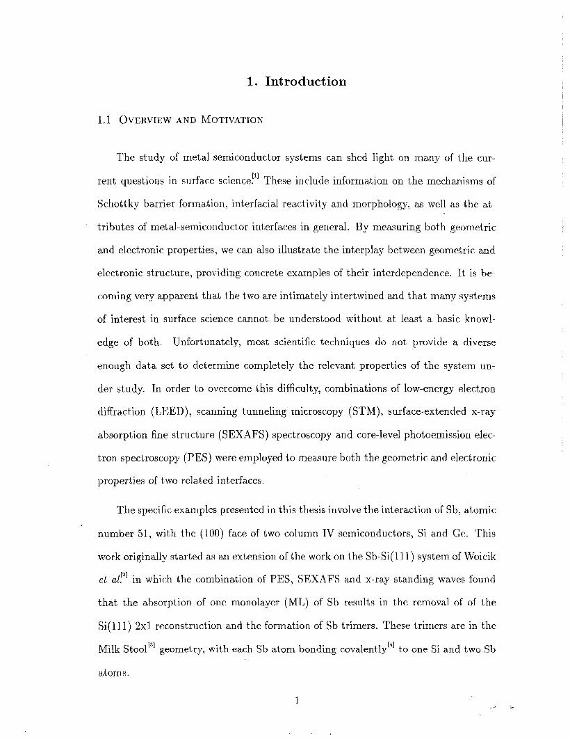
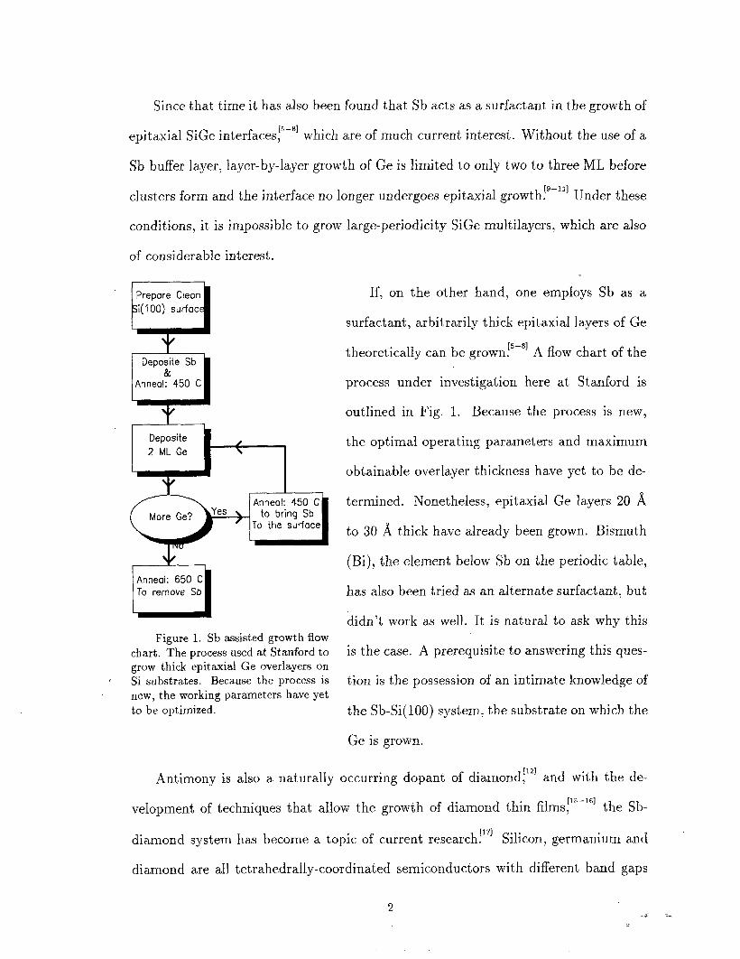
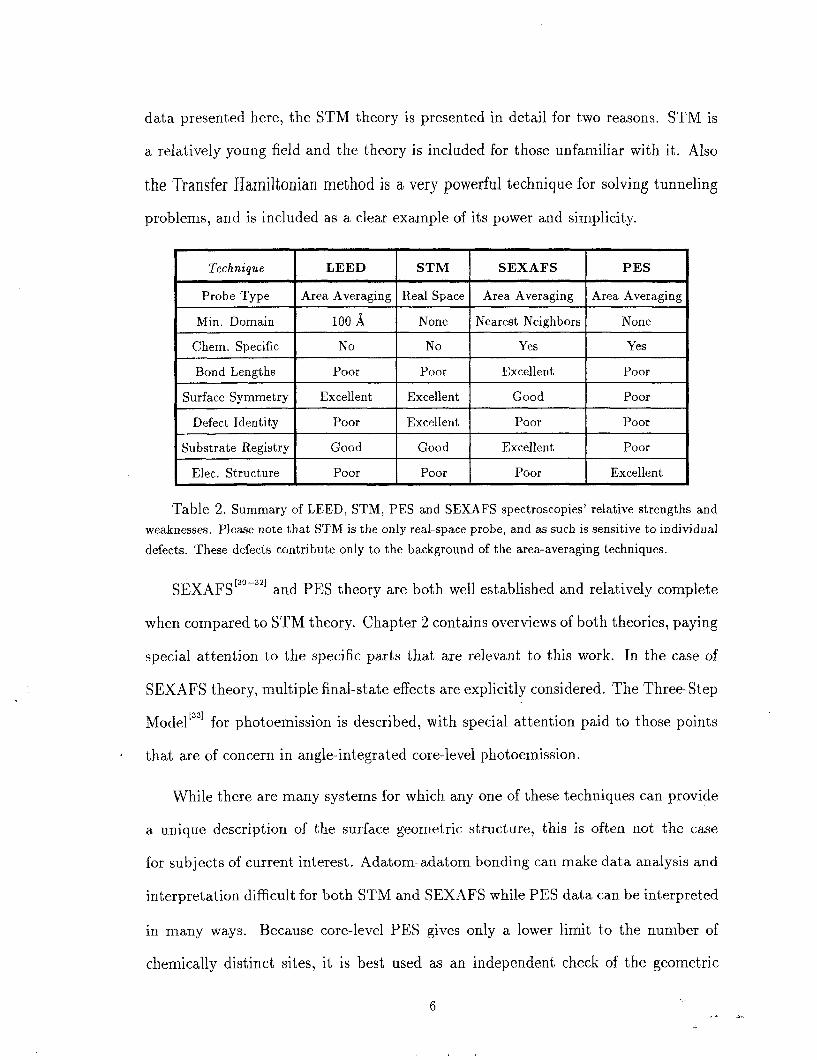


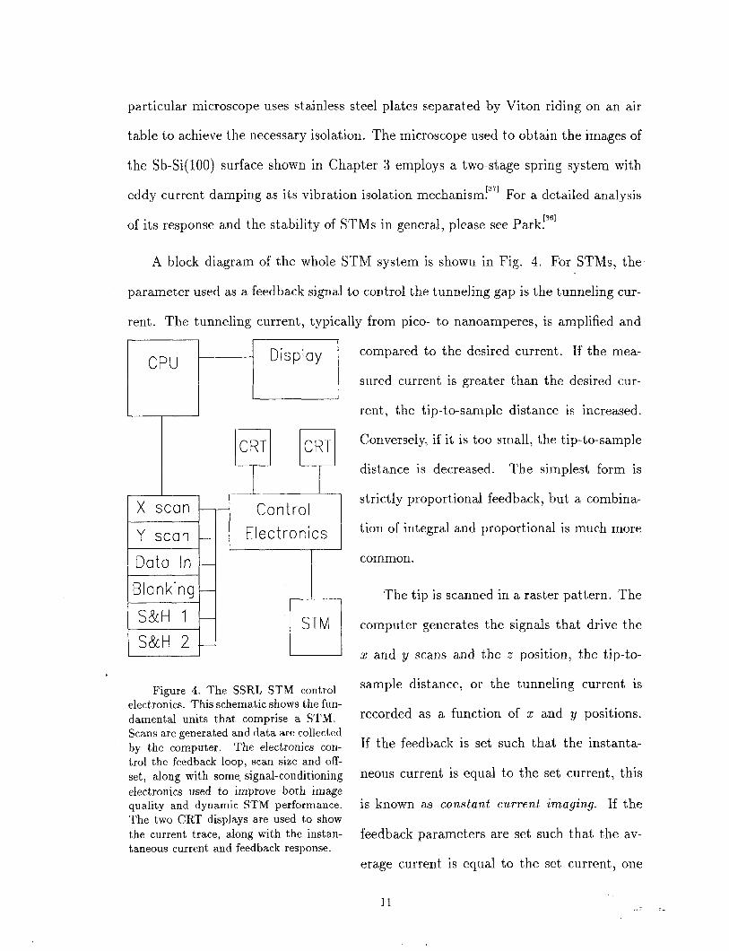
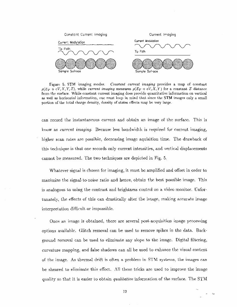
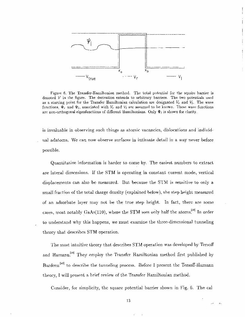

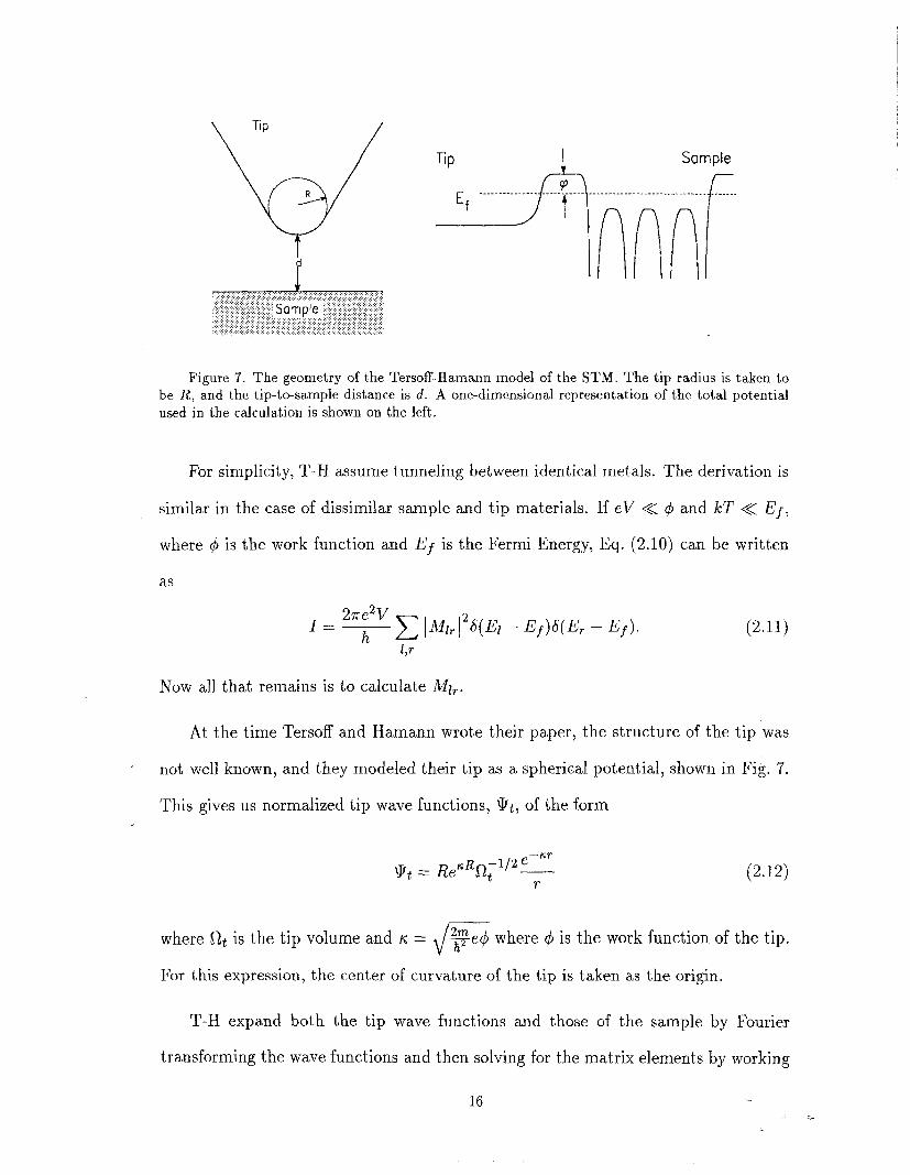

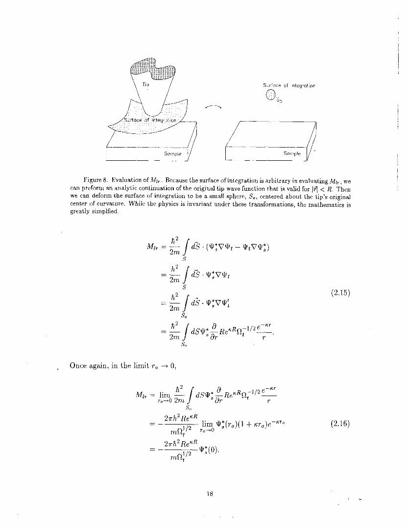


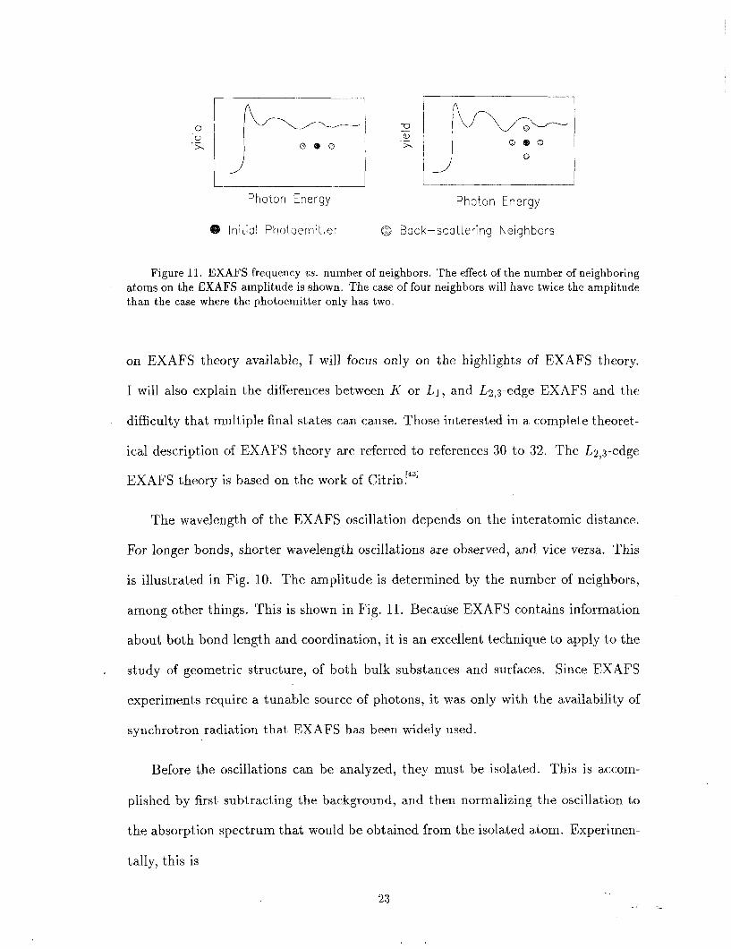
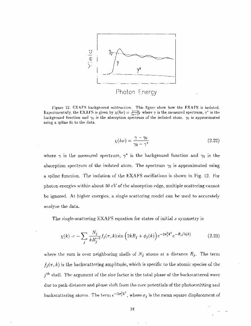
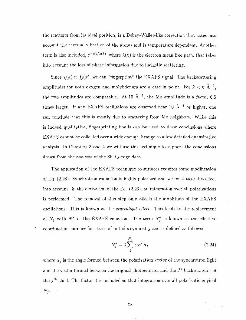
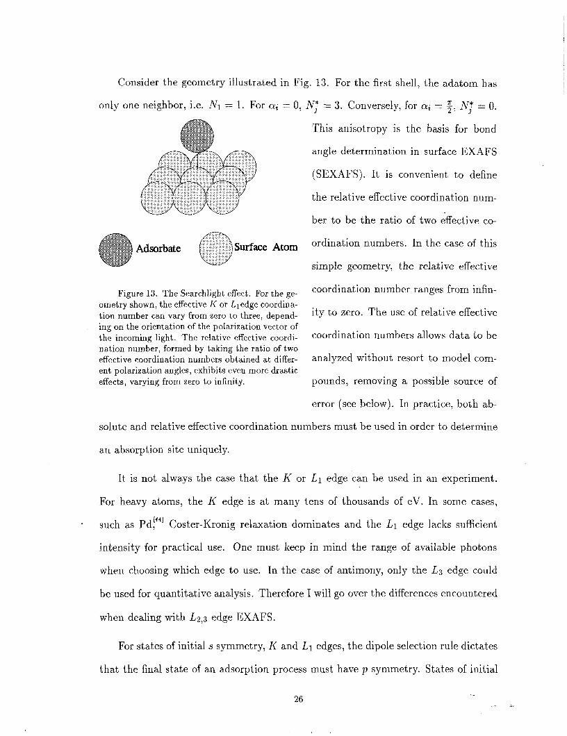

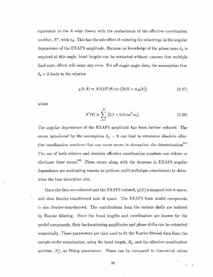
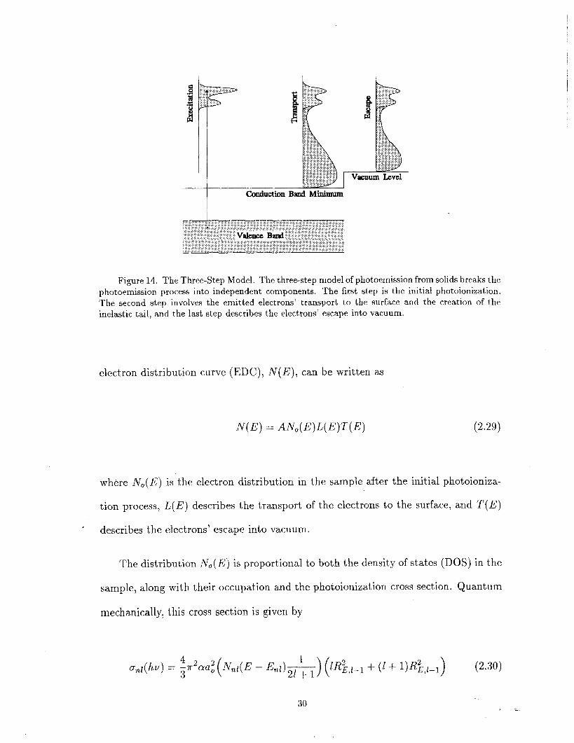


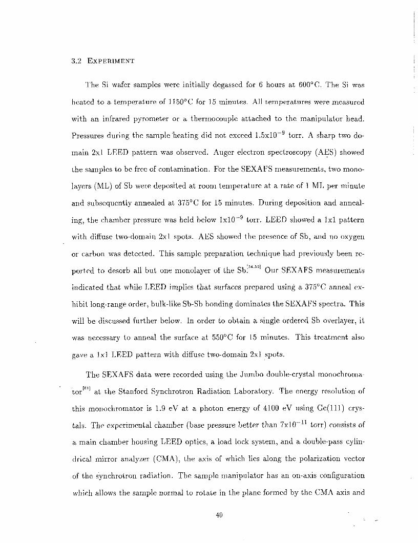
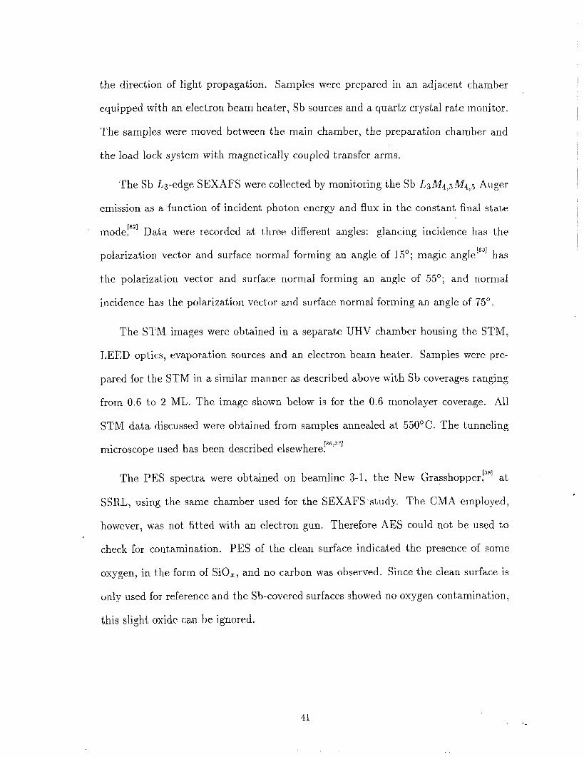
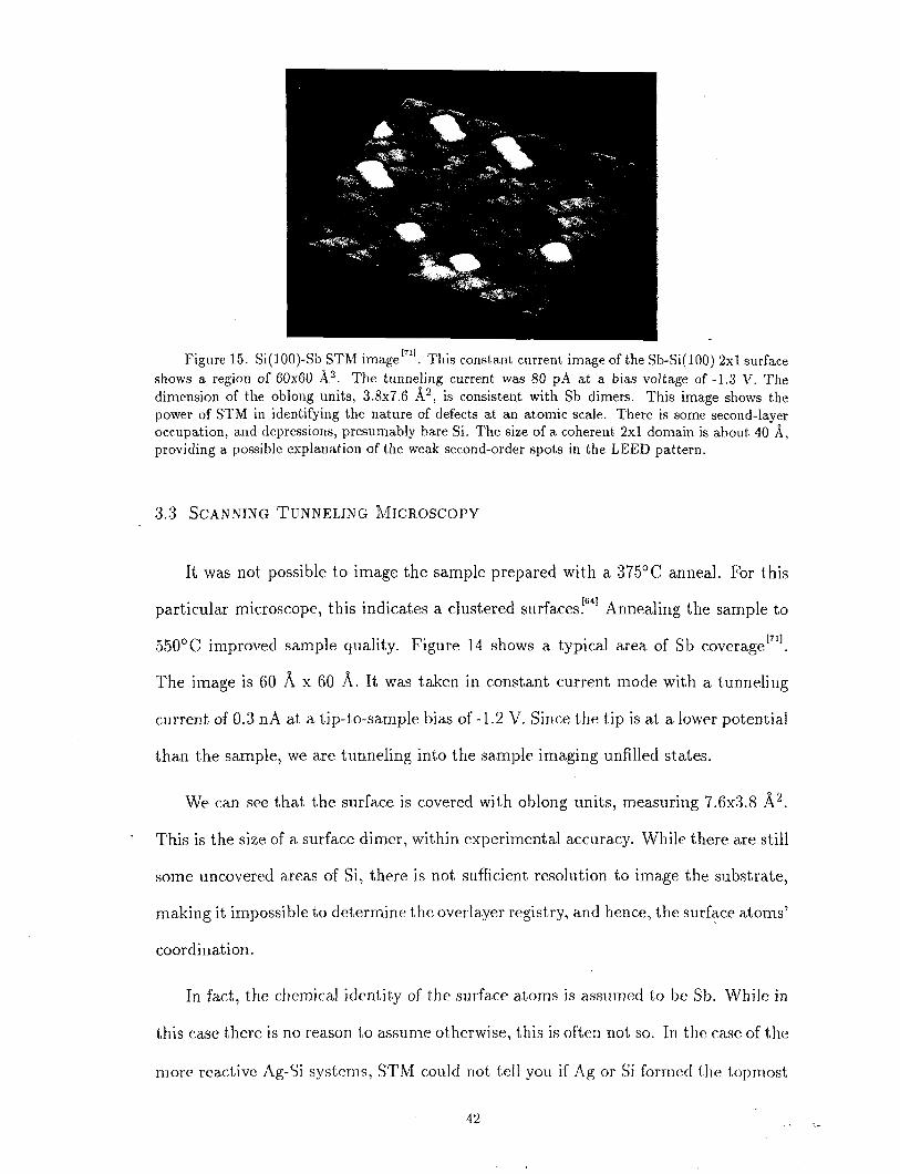
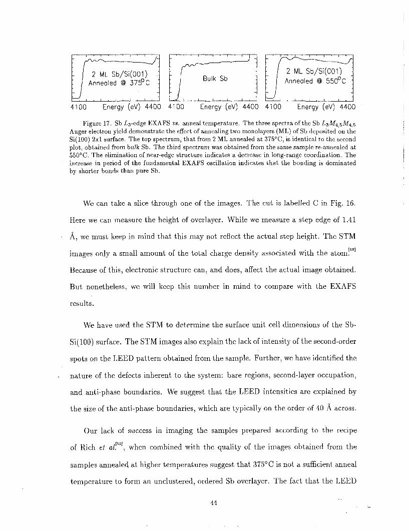
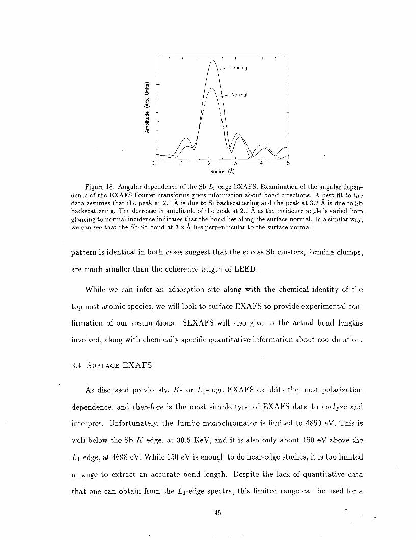
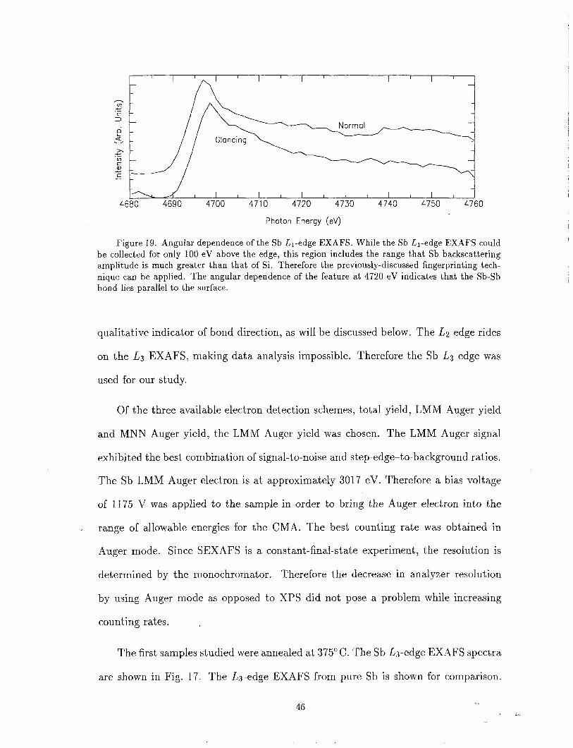
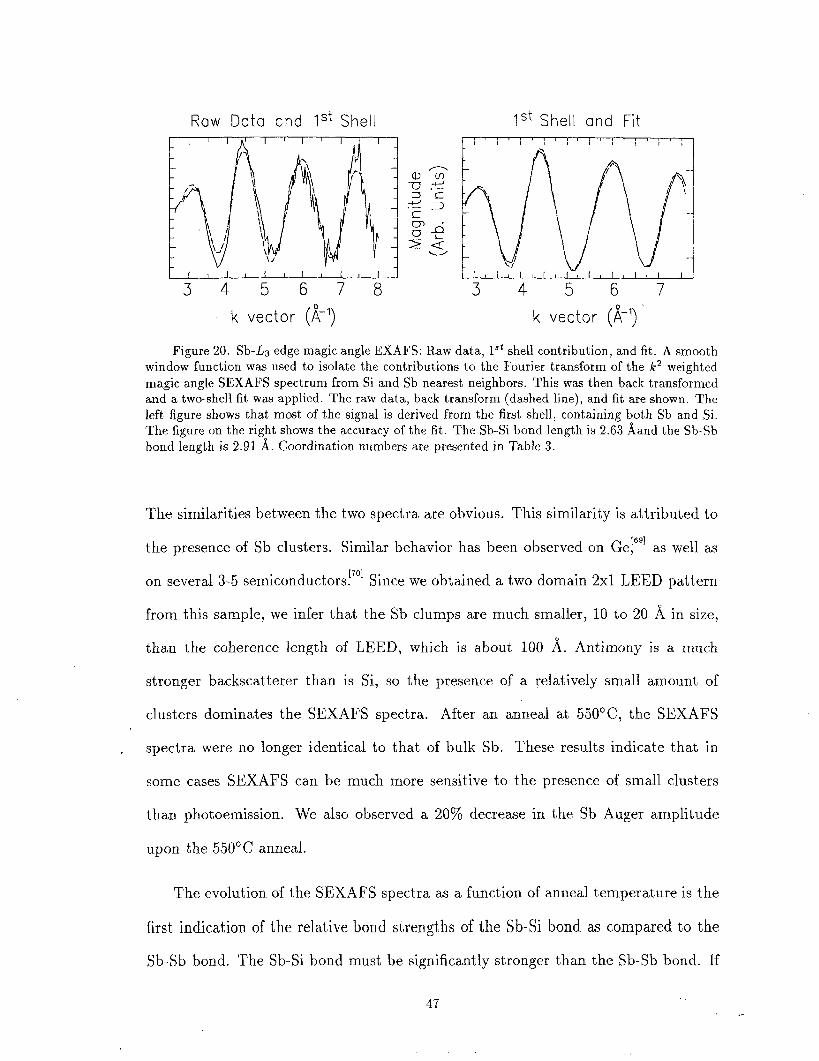
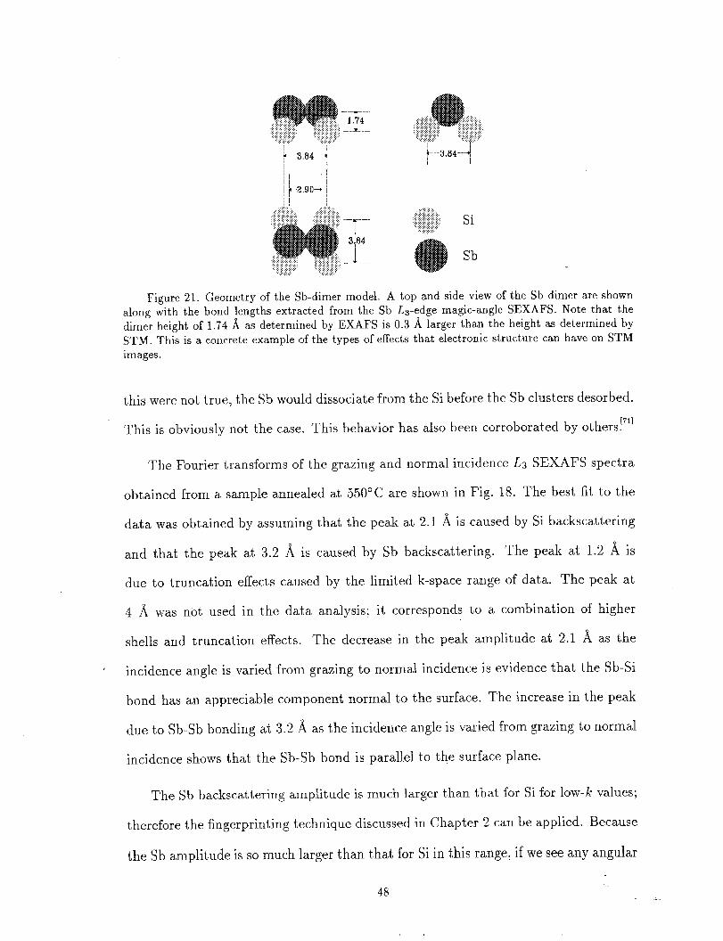
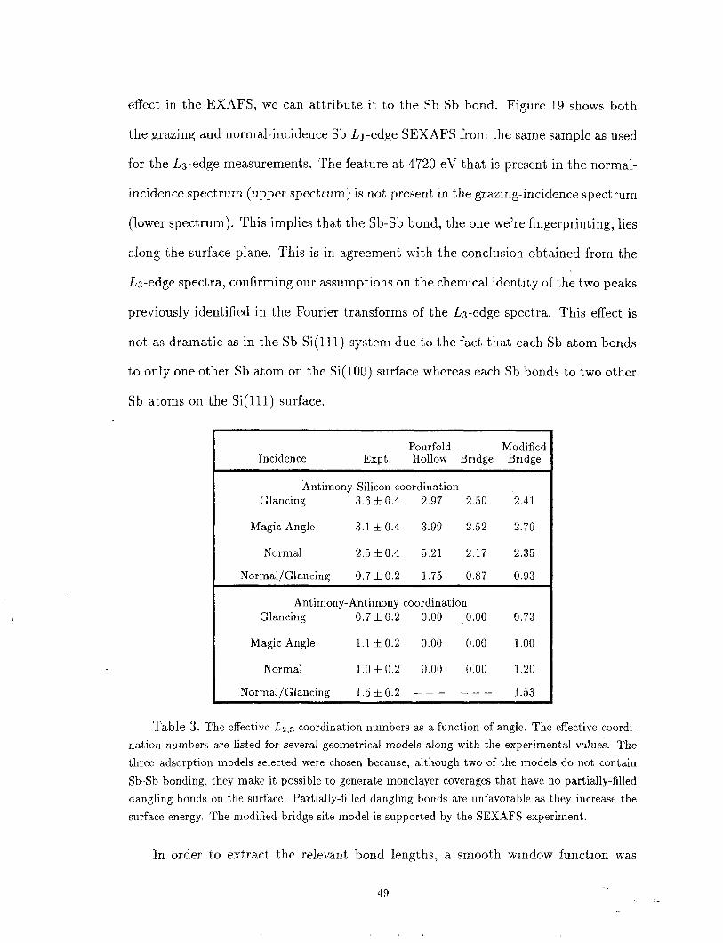
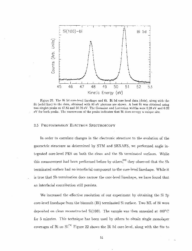
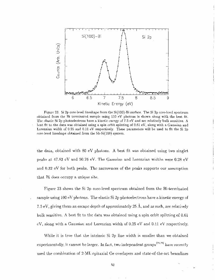
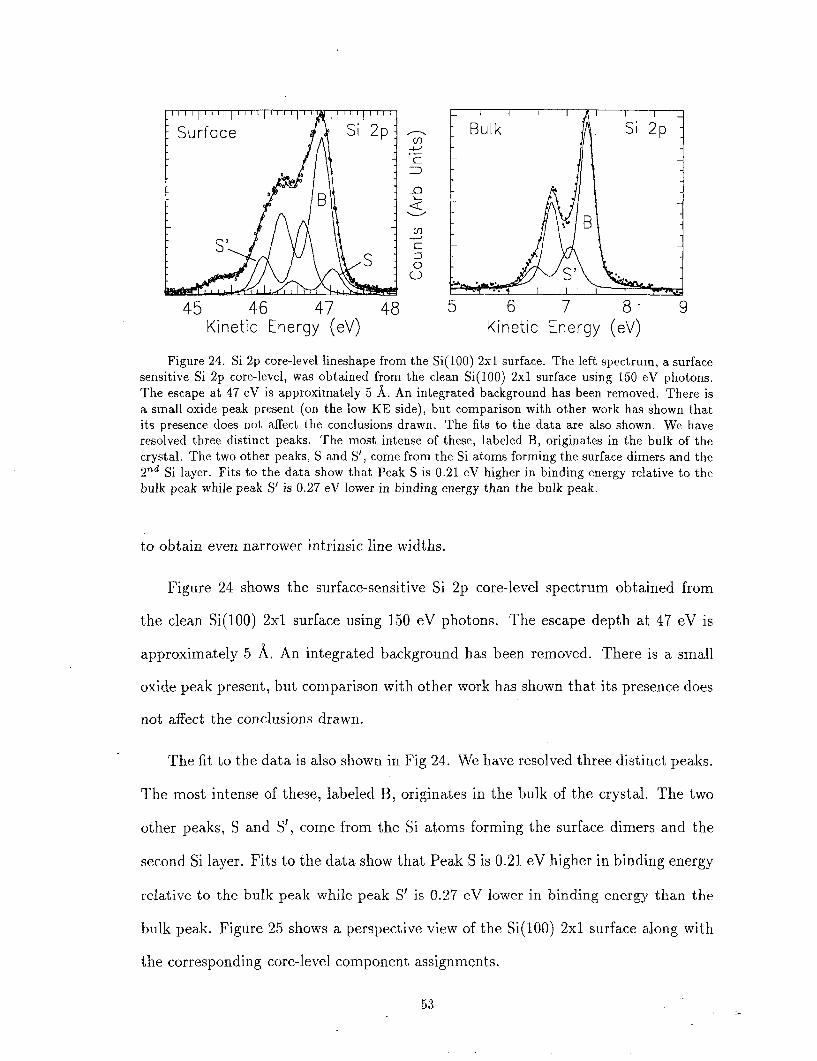
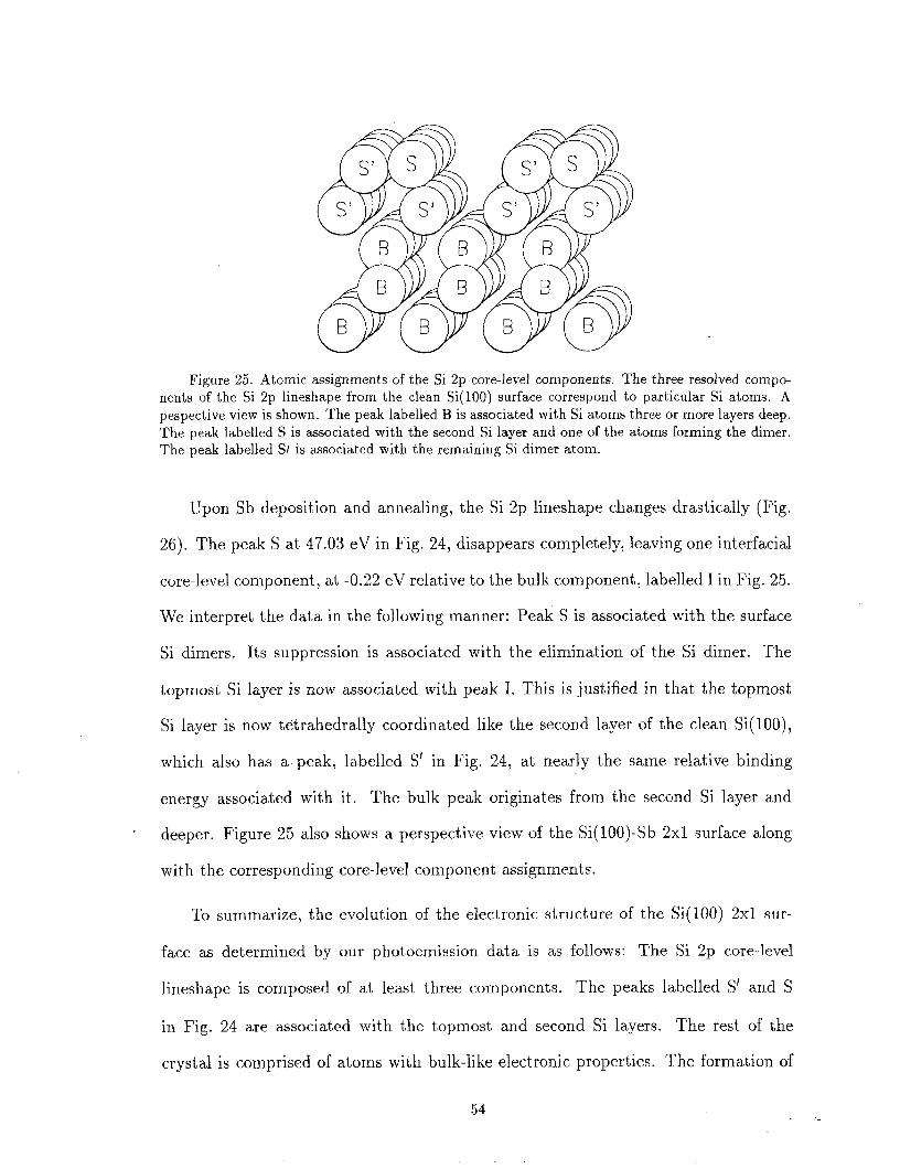
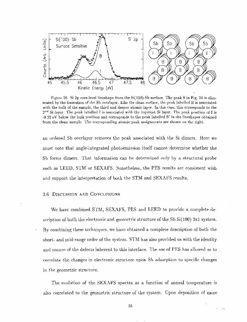
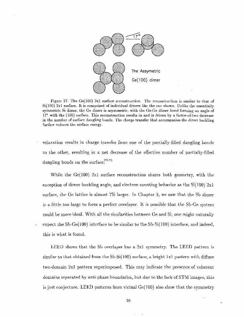

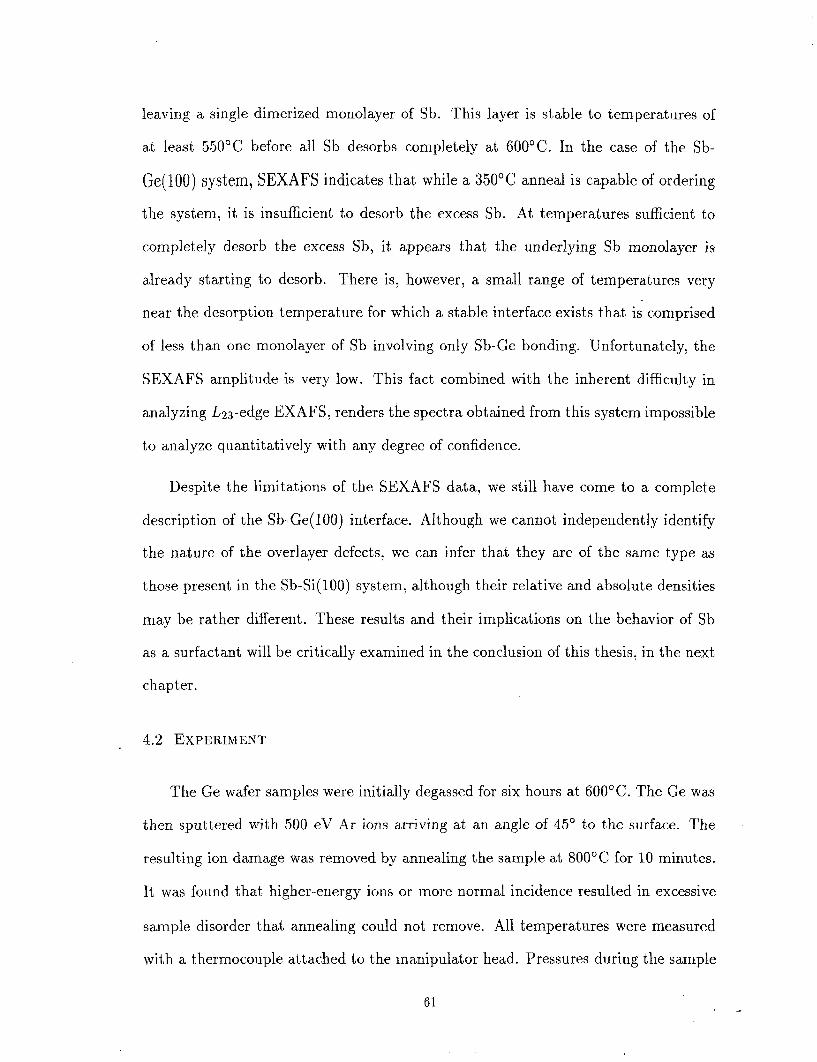

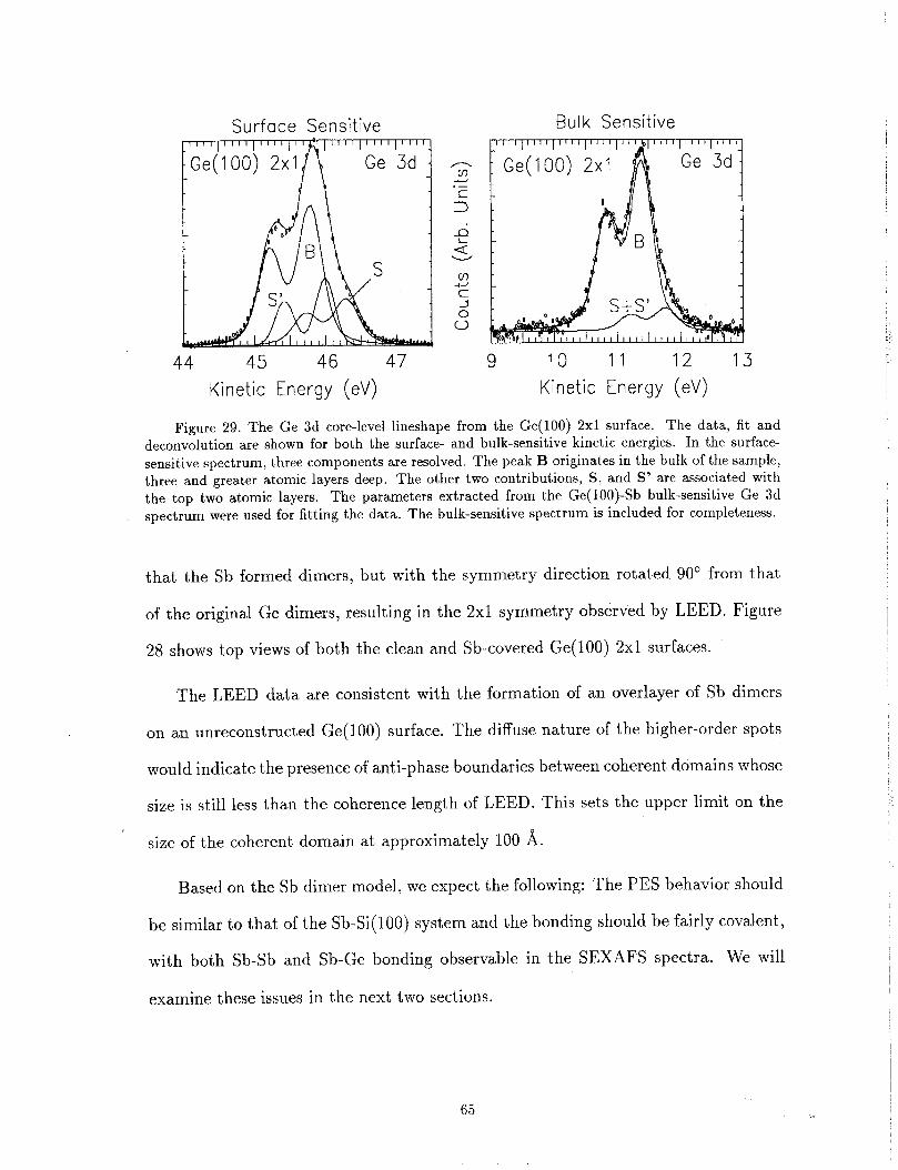
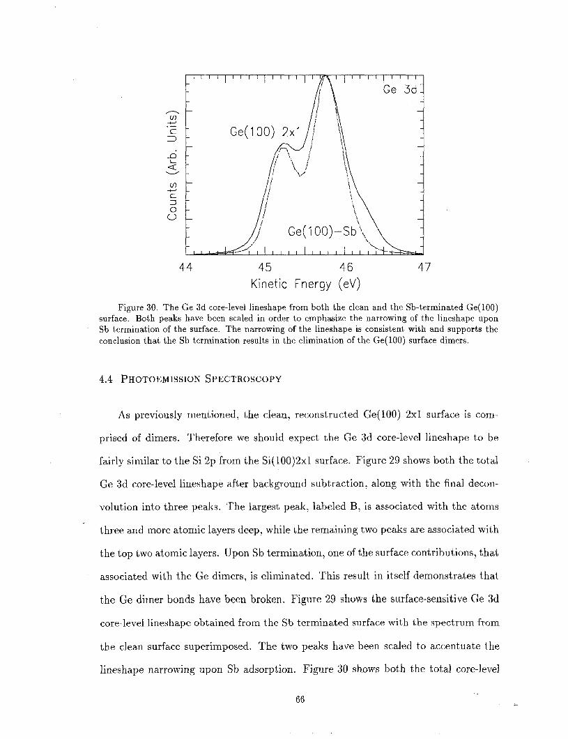
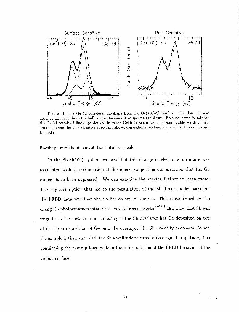
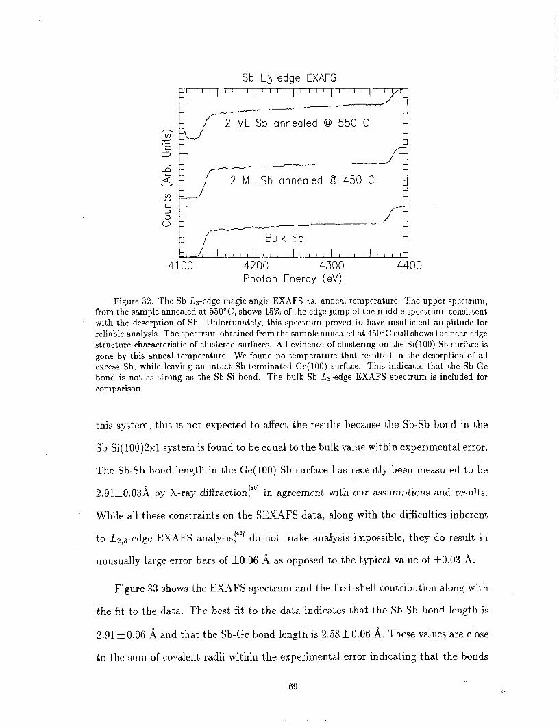
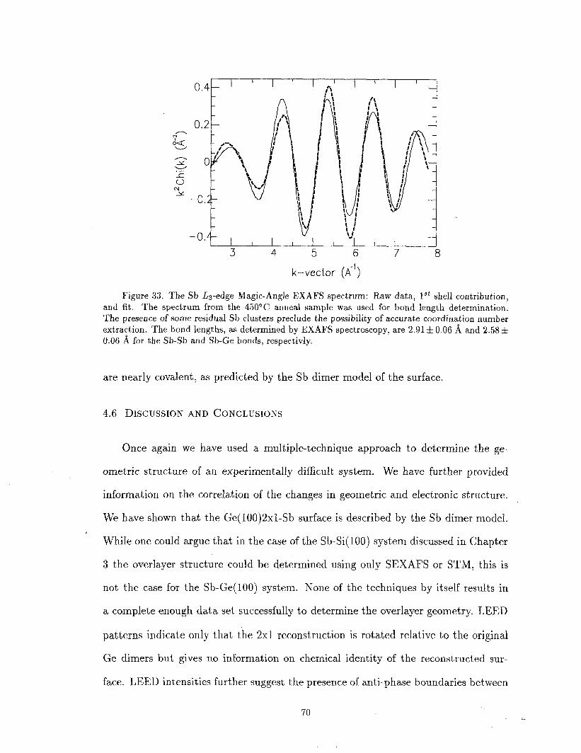
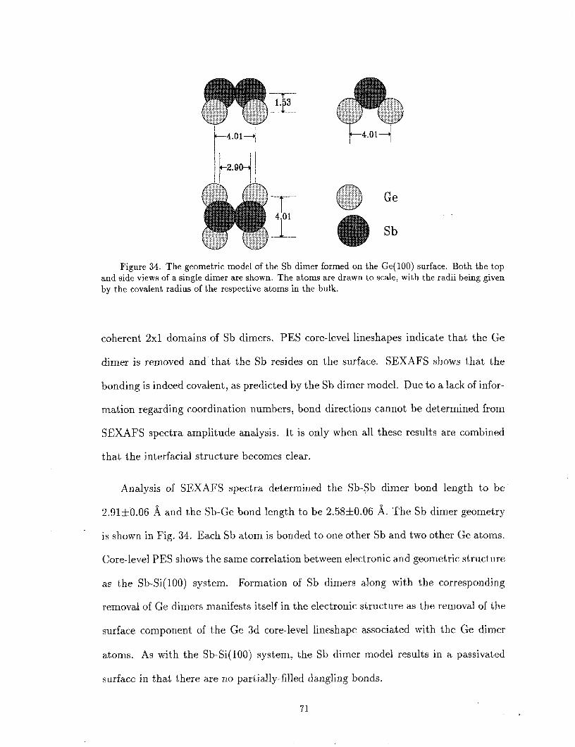
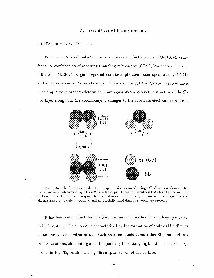

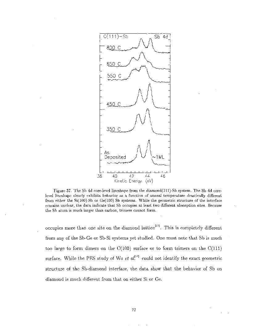


![Phase Lock Loo]](https://static.documents.pub/doc/80x56/577d1f281a28ab4e1e8fff25/phase-lock-loo.jpg)


