EIPC SPEeDNEWS The Weekly On-Line Newsletter from the European Institute of Printed Circuits. Issue 27 - September 2014 NEWS FROM AUSTRIA Piu Printex Announces the Purchase and Installation of the Chemplate Materials SL Indubond 130N Registration System Piu Printex, a quick turn-around, high mix manufacturer of high technology Printed Circuit boards of ever increasing complexity, located in Vienna, Austria, announced the acquisition and successful implementation of Chemplate Material SL’s Indubond 130N Inductive Registration System. Piu Printex’s Circuit Board Technical and Business Manager, Georg Pohanka, cites the need for extremely high registration precision for his customers’ multilayer circuits. Piu Printex must manufacture circuits of up to 40 layers including high TG / Low Signal Loss / Impedance Controlled Multilayers containing FR4 as thin as 50 micron as well as exotic materials such as Rogers, Arlon, Isola P96 (P97) and copper-clad Aluminium Core. The demanding registration requirements of Piu Printex’s customers, who require boards of up to 5 mm thickness with annular-ring tolerances of 100 micron or 0,004” (4 mil), sent Mr. Pohanka on an exhaustive search for and evaluation of the state-of-the-art in registrations solutions. A series of comparative testing against competitive bonding systems (from North America and Europe) led to the selection of the Indubond 130N System. “The combination of simplicity of the process, flexibility to bond any materials in any thickness we require, the cleanliness of any
Transcript
EIPC SPEeDNEWS The Weekly On-Line Newsletter from the European Institute of Printed
Circuits. Issue 27 - September 2014
NEWS FROM AUSTRIA
Piu Printex Announces the Purchase and Installation of the Chemplate Materials SL Indubond 130N Registration System
Piu Printex, a quick turn-around, high mix manufacturer of high technology Printed Circuit boards of ever increasing complexity, located in Vienna, Austria, announced the acquisition and successful implementation of Chemplate Material SL’s Indubond 130N Inductive Registration System. Piu Printex’s Circuit Board Technical and Business Manager, Georg Pohanka, cites the need for extremely high registration precision for his customers’ multilayer circuits. Piu Printex must manufacture circuits of up to 40 layers including high TG / Low Signal Loss / Impedance Controlled Multilayers containing FR4 as thin as 50 micron as well as exotic materials such as Rogers, Arlon, Isola P96 (P97) and copper-clad Aluminium Core. The demanding registration requirements of Piu Printex’s customers, who require boards of up to 5 mm thickness with annular-ring tolerances of 100 micron or 0,004” (4 mil), sent Mr. Pohanka on an exhaustive search for and evaluation of the state-of-the-art in registrations solutions. A series of comparative testing against competitive bonding systems (from North America and Europe) led to the selection of the Indubond 130N System. “The combination of simplicity of the process, flexibility to bond any materials in any thickness we require, the cleanliness of any
mass-lam process and the excellent design and workmanship we found upon evaluating the Indubond 130N” said Mr. Pohanka, “not to mention the excellent price/performance ratio and fast ROI, led us to make the decision for this system.” PIU-Printex GmbH is located at: Percostraße 18 A-1220 Vienna, Austria Georg Pohanka can be reached at: [email protected] Chemplate Material SL is located at: Pol. Ind. Can Bernades-Subirà, Carrer Empordà, 23, 08130 Santa Perpètua de Mogoda, Barcelona, Spanien
EIPC SPEeDNEWS The Weekly On-Line Newsletter from the European Institute of Printed
Circuits. Issue 27 – September 2014
NEWS FROM DENMARK
NOISE, EMI & SIGNAL INTEGRITY
Invitation to world-class event - Seminar with Richard Hartley Knowing how to design circuit boards to contain and control energy (fields) and knowing how to mitigate and control the effects of high speed devices is the key to successful design of low noise circuits. This 2 day workshop by Richard Hartley is a crisp focus of the issues PCB Designers and Engineers need to know to prevent signal integrity, EMI, crosstalk and grounding problems in high speed digital and mixed signal designs. This will be Richard Hartley’s first time in Denmark. He has dedicated the past 40 years to PC boards and circuit development with emphasis on control of noise - in both Digital and RF circuits. This is truly a great experience to learn from the best and network with people from the industry. Richard Hartley is from USA, and is recognised in the PCB industry as ‘one of a kind’. He is a Senior Principal Engineer at L-3 Communication, Avionics Systems and has his own company RHartley Enterprises where he consults and teaches. This is a “must-attend” event! WHAT YOU WILL LEARN This 2 day seminar will give you: • Skills to lower the EMI signature of your system. • Techniques that will improve the chance of your PC boards working the first time, all without noise or EMI problems.
• Learn the exact causes of noise and signal integrity, exactly why it happens and how to prevent it from occurring. • Learn not only what to do, but ‘why’ the techniques always work. • And much more! VENUE Radisson Blu - H.C Andersen. Odense, Denmark 19.-20. November 2014 € 1500 excl. hotel € 1750 incl. hotel (2 nights) SIGN UP You can sign up at: www.azitech.dk/events If you have any questions or want more information, please call Maria Justesen at +45 69 66 33 10 or write her an e-mail: [email protected]
EIPC SPEeDNEWS The Weekly On-Line Newsletter from the European Institute of Printed Circuits.
Issue 27- September 2014
NEWS FROM NORWAY
NORDIC HDI 2014 SEMINAR IN OSLO 22nd-23rd October 2014 at the Anker Hotel in Oslo. After a fully booked HDI seminar in Copenhagen in March 2014, we are now offering another opportunity to participate at this successful HDI seminar with Happy Holden. Mr. Holden will introduce you to HDI and its unique design opportunities and with his vast experience from Foxconn, he will teach you how to use HDI correctly and efficiently in your products. Azitech is happy to announce that all education materials used at the seminar, including Mr. Holden’s book “the HDI Handbook”, can be ordered by seminar participants –free of charge. For more information check out www.azitech.dk/events or give us a call at +45 66 13 07 68
EIPC SPEeDNEWS The Weekly On-Line Newsletter from the European Institute of Printed
Circuits. Issue 27 - September 2014
NEWS FROM THE UK
ISOLA & HOLDERS TECHNOLOGY SEMINAR WORCESTER RUGBY FOOTBALL CLUB, TUESDAY 16TH SEPTEMBER 2014
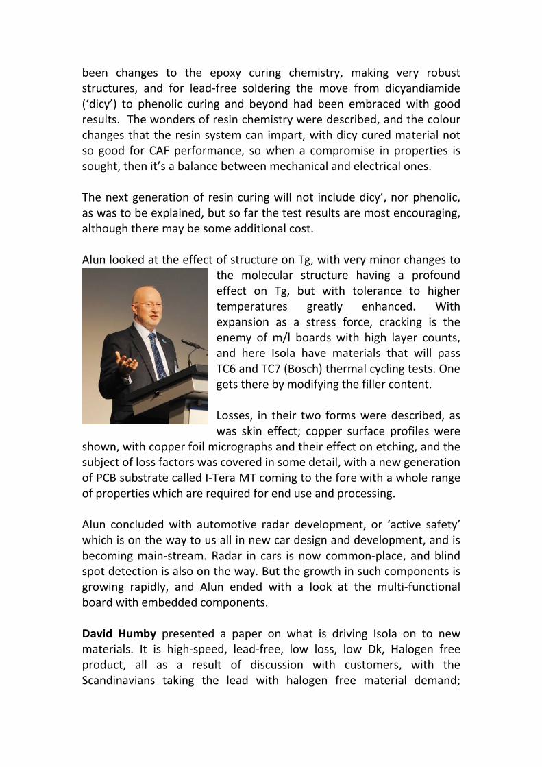
It was Angus Brunton who welcomed the many delegates to the joint technical seminar being held by Isola and Holders Technology in the imposing conference rooms at the Worcester Warriors RFC. The aim was to introduce some new products from Isola, and some of the products sold in the UK by Holders Technology. Angus reminded us that Isola have been making copper-clad laminate since 1956, a time when a few other holes were being drilled in the area around the Suez Canal. Whilst the Middle East has been steadily going backwards ever since, Isola have been going fast forward with an acquisition campaign and is a truly international company with the Far East covered from their offices in Hong Kong and five manufacturing plants in Asia, North America from their HQ in Chandler, Arizona, with three manufacturing plants in the USA, and Isola in Duren, Germany overseeing two in Europe, with the R&D back in Chandler. Alun Morgan then explained the key technology focus areas – first up was high speed digital, operating up to 100GHz, which was presenting challenges to materials; then came Halogen free materials, required especially for base stations; automotive safety is demanding new materials, too, and CAF, and speciality areas. With a reminder on how CCL is constructed, Alun said that the three components each play a critical role in the ability of manufacturers to modify the end product to suit the requirement of end use. There have
been changes to the epoxy curing chemistry, making very robust structures, and for lead-free soldering the move from dicyandiamide (‘dicy’) to phenolic curing and beyond had been embraced with good results. The wonders of resin chemistry were described, and the colour changes that the resin system can impart, with dicy cured material not so good for CAF performance, so when a compromise in properties is sought, then it’s a balance between mechanical and electrical ones. The next generation of resin curing will not include dicy’, nor phenolic, as was to be explained, but so far the test results are most encouraging, although there may be some additional cost. Alun looked at the effect of structure on Tg, with very minor changes to
the molecular structure having a profound effect on Tg, but with tolerance to higher temperatures greatly enhanced. With expansion as a stress force, cracking is the enemy of m/l boards with high layer counts, and here Isola have materials that will pass TC6 and TC7 (Bosch) thermal cycling tests. One gets there by modifying the filler content. Losses, in their two forms were described, as was skin effect; copper surface profiles were
shown, with copper foil micrographs and their effect on etching, and the subject of loss factors was covered in some detail, with a new generation of PCB substrate called I-Tera MT coming to the fore with a whole range of properties which are required for end use and processing. Alun concluded with automotive radar development, or ‘active safety’ which is on the way to us all in new car design and development, and is becoming main-stream. Radar in cars is now common-place, and blind spot detection is also on the way. But the growth in such components is growing rapidly, and Alun ended with a look at the multi-functional board with embedded components. David Humby presented a paper on what is driving Isola on to new materials. It is high-speed, lead-free, low loss, low Dk, Halogen free product, all as a result of discussion with customers, with the Scandinavians taking the lead with halogen free material demand;
amongst their new materials are I-Speed, I-Tera MT, GreenSpeed, 185HR, with others under launch at the moment. Alternative materials to PTFEs are now available to designers. Products include GigaSync, for high-speed application, which has very high thermal performance. Also, there are I-Speed, I-Speed IS, Tachyon, and IS680, a very low Dk material for RF and microwave applications. I-Tera MT is a very versatile material, with applications in many fields; it has no filler, has a lower dissipation factor, long shelf-life, good cost benefit, and this is made in the USA, in 50” width, with square weave styles, and 2micron copper as standard. TerraGreen is an ultra-low loss halogen-free option, targeted for backplanes, base station applications, cloud computing, with many good properties including thermal reliability and compatibility with lead-free specifications. Tachyon is the next generation of ultra-low-loss laminates, low Dk, as close as you want to PTFE, with very good thermal performance, and easy drilling, Astra MT is a low Dk 3.0 Dk, ideal for the RF/Microwave areas, including automotive radar and sensors; it is available in a limited range of thicknesses, with a good CTE. Jürgen Knörchen of Holders Technology in Germany wanted to talk about Pacomask. This is a patented, engineered adhesion system between mask and subsequently between the press plates to provide complete protection throughout the entire cycle of PCB lamination process. The adhesion formulation assures a residue-free copper surface on copper clad laminates and separator plates after processing, it significantly improves handling of thinnest copper foils, it speeds the lay-up process and is suitable for all automated handling systems. The end result is a clear, clean, protected copper foil surface, free of epoxy dust, dirt or any other contamination. It has a tolerance of operating temperatures up to 195°C for up to 90 minutes, and the 3 mil film can be applied to copper sheets or rolls of 5 - 70µ CAF – this is not an abbreviation of ‘caffeine’ but a phenomenon that keeps many people awake more effectively. Alun Morgan took us back to the 1970’s when a sudden loss of insulation resistance was seen in
circuit boards which had been subject to hostile operating conditions. Bell Laboratories took up the cudgel of investigating this, and found that the physical degradation of the glass/epoxy bond was permitting moisture absorbtion in conditions of high humidity, and electrochemical corrosion followed. CAF is an electrochemical process, and requires three things – water – voltage bias, and a way for ions to move from the anode to the cathode. High moisture, high voltages and high temperatures can all lead to CAF. Alun explained the test methodology which is not standardised at the moment. He illustrated the CAF resistance plot, with infantile failures, though to wear out failures, and examples where CAF had spread across between holes. Dicy cured laminates proved to be the worst for CAF failure. With unreacted hardener being the culprit, but the advent of lead-free led to phenolic curing and the reduction of CAF failure. Design, materials and process all are CAF elements – the sourcing of components, the number of appliances per part, the number of glass layers, etc and then there are laminate fabricator issues, such as the glass cloth, the resin formulation, the laminate thermal resistance, Factors affecting CAF resistance include gap, voltage, curing system, the board shop, orientation, glass weave, reflow, Tg, a mixture of design and materials. The need is to look at the effects that laminate materials, design, and the PCB manufacturing company processes, all of which can have an impact on CAF. A bad fabricator can make a good material bad, but good manufacturers cannot make a bad material good. Says it all, really. Angus Brunton came back again with a couple of videos; the first was about their Global Analytical Service Laboratories, and he then introduced the IsoDesign service from Isola, a web-based system onto which one merely registers to obtain a design service for high speed digital design needs. This is a 24 hour on-line service. Then Detlev Kübler the boss of Holders Germany to talk about Doosan Electro Materials. Doosan was established 118 years ago, and the Doosan Group is one of the top ten in Korea. Revenue has gone from $3.8 billion in 1998 to $23.6$ by 2012, and this is based on growth by acquisition; they took over Circuit Foil in Luxembourg for example.
Currently they are now No.3 in in packaging material supply to the memory market. Heavy copper clad material capacity has done well, and their flexible CCL has risen from a modest 490 sq. metres per month to 1 billion per month this year. They offer flexible copper clad laminate, including prepreg, coverlays, and have a single-step copper clad laminating line, against the competitor’s 3-stage coating system, but with their double sided material they follow more conventional lines. Mr Kübler described the transition loss properties of the flex CCL range, and he looked at the polyimide range of flex circuitry materials; here the Doosan range is superior, with better peel strength, transparency and soldering after moisture absorbtion. They also offer RA copper, available in both single and double sided formats. Reading from the First Book of Laminations, Alun Morgan came to enlighten us about glass fabric production and developments. We got to handle a lump of resin, a bundle of yarns, and we were informed about such things as ‘high tensile strength’, ‘dimensional stability’ and ‘high thermal resistance’ etc. The glass fibres are known as e-glass, made from various metal oxides which are fired at some 3500ᵒF. Yarns have differing diameters, 5-9 microns in diameter, (human hair is 100 microns, just as a guide). Finishing and treating the yarns was described, it’s a complex process, with an enormous range of style, thread diameters, and the permutations of warping and wefting seemed endless. There is a relationship between dielectric constant and yarn content, and the features now of a board can correspond with the features of the fibres, so the selection of thread count is important. A square weave is favoured for digital designs. This was a very detailed presentation on glass, fibres, and how these fibres play such an important part in determining the suitability of a laminate for a particular function. The last speaker of the day was Ian Fox of Controls and Data Services at Rolls-Royce. His company manufacture aero engine controls. Harsh environments is what they know about – with very high temperatures or very low ones, with high humidity, or low humidity, salt, dust, NOx and SoX. And, of course, vibration. Aero engine controls sit right on the engine casing, and operate under very high temperatures. It is when operating temperatures are above
150ᵒC that Mil-Specs come into play. Above 200ᵒC and above 300ᵒC Silicone carbide is used but that’s expensive. In the field of solder alloys, eutectic SnPb is not good for operations at 150ᵒC +, so they can modify alloys to suit. ENIG as a finish is fine, and above 150ᵒC a polyimide PCB is required. Assembly can be machine soldered using conventional reflow. High Pb content alloy is used with temperatures of between 175ᵒC and 225ᵒC, an AuSn alloy is fine but processing is difficult and has a very steep liquidus line. For all practical purposes 225ᵒC is the upper operational temperature limit for laminate base designs. Ian listed the factors involved with the environmental protection of assemblies; post assembly cleaning is vital, and a conformal coat is needed to prevent oxidation and corrosion. Hermetic microelectronics is the way forward, said Ian. Co-fired ceramic packages with integral substrate are either HTCC or LTCC, the HTCC has high thermal conductivity but at higher cost. The Low Temperature Co-fired Ceramic is more cost effective. For service temperatures of above 250ᵒC die attachment works well, with cyanate ester adhesives, and Ag sinter materials for bonding. A hermetic package can be sealed with soldering, either by ultrasonic soldering, or liquid phase sintering. Aluminium wire bonding is fine below 250ᵒC but above that full mono-metallic bonding is required. The package atmosphere is critical to reliability, and what makes it secure is avoiding outgassing, so that H2O is absent. This can be determined by a Residual Gas Analysis (RGA). Ian concluded with a mention of Transient Liquid Phase Sintering, a Physics of Failure approach carried out by CALCE at the University of Maryland. The process uses Sn-rich alloy with Cu and SN parties mixed with flux and used to print the SMT devices and then sintered, and this gives a very solid and secure joint. The predominant intermetallic is Cu6Sn5 with a melting point of 415ᵒC. This survived 500 cycles of shock test 1500G with no cracking and 2500 G with no separation.
L-R David Humby, Alun Morgan, Detlev Kübler, Jürgen Knörchen, Ian Fox, Angus Brunton.
This was a timely and well-considered seminar that was of obvious appeal to the technical management of the major companies in the UK PCB industry, and in true Isola style it was all done very well. John Ling Editor
Ventec Europe Continues FOD-Avoidance Investment Programme
The avoidance of foreign object contamination continues to be a fundamental objective in Ventec Europe's UK prepreg fabrication facility, and the company is proud to announce that its epoxy prepreg cutting and slitting department has been brought to the same standard of clean-room operation as already established for its polyimide prepreg.
The latest Pasquato slitter-sheeter installation has been specifically designed to aerospace standards to eliminate the possibility of debris and dust entrapment. As in the polyimide department, production procedure is that once a prepreg roll is transferred from cold store to slitting machine, the whole roll is slit so that there is no backwards-and-forwards traffic of part-rolls. And the prepreg comes out of the clean room in the form of sealed aluminised packs for delivery straight to the customer's lay-up room.
Mark Goodwin, Ventec's Chief Operating Officer for Europe and USA commented: "This represents the latest stage of a structured investment programme and demonstrates our commitment to reducing FOD risk for our mil/aero customer base and managing delivered quality to the highest standards. The next stage will be the installation of Class 6 clean room canopies over each of our slitter-sheeter machines, to be completed within the next few weeks, as part of our support for the European Space Agency's campaign to drive up cleanliness standards to the new IPC-4101-D Appendix A"
ITRI Innovation is holding a free industry day event ‘21st Century Solutions for PCB Assemblies’ on Tuesday 28th October 2014 in St. Albans in Hertfordshire ITRI Innovation is holding an industry day event ‘21st Century Solutions for PCB Assemblies’. This event aims to assist companies with finding out how to resolve technical issues quickly, bring products to market faster and gain peace of mind through testing. It will take place on Tuesday 28th October 2014 at ITRI Innovation Laboratories, St. Albans in Hertfordshire and there is no cost to attend this event.
By holding this event at ITRI Innovation, delegates will be able to tour the laboratory and see the test equipment which is available. For a limited number of companies, there is an opportunity to have some complimentary sample testing carried out in advance of the day and then the chance to discuss the results at the event. Companies interested in this opportunity can contact Dr. Wayne Lam (Laboratory Manager) by email: [email protected] to discuss it further.
“We understand that the electronics industry is continuing to face many challenges. Through offering this exclusive event, we aim to meet these by hosting educational seminars led by experts who have practical experience both in counterfeit detection and in developing quality control testing programmes to ensure component and assembly compliance;” comments Dominic Lodge, Manager, Solder Technology Division, at ITRI Innovation.
The event would be beneficial for manufacturers of equipment that incorporates electronic components and for professionals with roles in Research & Development, Technical and Engineering, Production and Quality Control. These can be from industries, such as aerospace and space, automotive, consumer electronics, defence, marine and medical. This industry day includes a light breakfast, luncheon and refreshments and will take place from 10am to 3pm. Companies requesting more information or wishing to register their details should contact: 01727 875544 or email: [email protected]. Further details can be found at: www.itrilabs.co.uk/events/21st-century-solutions-for-pcb-testing-services-open-day/
EIPC SPEeDNEWS The Weekly On-Line Newsletter from the European Institute of Printed
Circuits. Issue 27 - September 2014
NEWS FROM THE USA
WORLD PCB PRODUCTION IN 2013 ESTIMATED AT $59.4 BILLION IPC World PCB Production Report Released The world market for PCBs declined an estimated 2.2 percent in real terms in 2013, although real growth in North America was positive at 0.8 percent, according to IPC’s World PCB Production Report for the Year 2013. Developed by a team of the world's leading PCB industry analysts, the annual study is the definitive source of PCB production data, indicating what kinds of PCBs are being made where. World PCB production in 2013 was valued at an estimated $59.4 billion. The IPC report contains estimates of 2013 PCB production value by 10 product categories and by 31 countries or sub-regions. PCB values of standard multilayer and integrated circuit (IC) package substrates are segmented by those having microvia structures and those with non-microvia structures. New in this year’s report is a further subdivision of flexible circuits into three sub-categories: one- and two-sided, multilayer and rigid flex. The report also includes updates on specialty laminates and metal-core PCBs, as well as historical data on regional shifts in PCB production. The data show that the worldwide flexible circuit market grew in 2013, while the rigid PCB market declined. Regional trends are also examined, including China's slowing production growth and Japan's fall from
second place in the list of top 10 PCB-producing countries to fourth place. Thailand and Vietnam experienced the highest growth in PCB production. Sharon Starr, IPC director of market research, explains, “Despite evidence of a small on-shoring trend in North America and Europe, most large companies still produce a substantial share of their PCBs off-shore.” The report shows that companies based in Taiwan, Japan and South Korea, for example, are responsible for nearly two-thirds of world PCB production. U.S. companies account for about 10 percent of world PCB production, although the United States has less than a 5 percent share of world production within its borders. World PCB Production Report for the Year 2013 is available to IPC members for $475; the price for nonmembers is $950. For more information or to purchase the report, visit www.ipc.org/world-pcb-report-2013. For information on IPC market research programs, visit www.ipc.org/IndustryData or contact Sharon Starr, at +1 847-597-2817 or [email protected]. IPC Study Examines Potential Spots for Global Expansion By Terry Costlow, IPC online editor When companies decide to expand their global operations, more than one region or country will often work. Weeding out extraneous data to get information that’s relevant for the decision-making process can be a very time-consuming task. IPC has published a study containing a wealth of data that’s relevant to companies in the electronics industry. Where in the World? A Regional Strategy Roadmap for Electronics Manufacturers is a 145-page report that covers 30 countries, providing a broad range of information for each. It lists major corporations that are in the area, while also describing regional trends that could impact future development. “This is a comprehensive resource for executives who are doing long-range planning on their global footprint,” said Sharon Starr, IPC’s director of market research. “It has detailed information on many factors that are specific to the electronics industry that will help them make informed decisions.”
The data was collected by BPA Consulting, a research firm that has worked with IPC for some time. The study is designed to help electronics manufacturers address three key needs: making things inexpensively in high volume to supply existing markets; fabricating intelligence/technology-rich products for mature markets where rapid response and flexibility are at a premium; and the potential for substantial new markets as gross domestic product (GDP) per capita increases. “From the late ‘90s to the early years of this millennium, China was an inexpensive area in which to grow production,” said Nick Pearne, director of BPA Consulting and author of the IPC study. “This balance is now shifting as the Chinese economy develops and the second and third factors are coming into play. However, it is clear that China will remain as the most massive manufacturing region for electronic interconnect and assembly for this decade and beyond.” The study also identifies the major assembly company operations located in each country and the technological and market “hot spots” throughout the world, and reviews on-shoring and off-shoring trends. Analysis of how nations handle intellectual property and how the overseas investment flows into each country indicate levels of confidence and enable industrial development is also included. The report was designed to convey the majority of information graphically, offering a comparative, standard format to enable rapid assessment of the relative potential of the covered economies. The report cites Mexico and Vietnam as two of the most attractive locations for interconnect and assembly. Mexico overshadows Brazil, which has made substantial progress in recent years. Brazil’s image matured when it successfully hosted the World Cup. But all in all, Brazil loses hands down to Mexico as a good manufacturing base. Countries east of Europe, notably the Czech Republic and Hungary, are proving very successful for fast response, high tech production. Ukraine also holds promise for Europe, but the ongoing turmoil with Russia could well prove extremely problematic for business.
EIPC SPEeDNEWS The Weekly On-Line Newsletter from the European Institute of Printed
Circuits. Issue 27 – September 2014
PRINTED ELECTRONICS NEWS
Structural electronics: a potential $60bn market by 2025 Electronics embedded within the structure of bridges, walkways, EVs, aircraft and more, have the potential to be a $60 billion market by 2025. Aircraft, and later cars, will have a nervous system like a human being, instantly alerting to touch and damage. Aircraft will have no passenger windows, instead displaying a moving colour picture of what you would see from a window in the position where the window used to be, thanks to a smart inside to the fuselage - an imaginary window. Bridges immediately warn of decay, load or earthquakes thanks to self-powered sensors sealed within them. Dance floors, stairs and the walkways in subways sometimes generate enough electricity to power signage and lighting because electronics sealed in the floor creates electricity from movement. All this is structural electronics, a large new market assessed in the unique new IDTechEx report, Structural Electronics 2015-2025: Applications, Technologies, Forecasts . This report, with many extensive, original tables and diagrams, gives ten year forecasts for structural electronics and for its key enabling technologies employed or envisaged such as printed electronics. Electric vehicles particularly need structural electronics so their numbers are forecasted for the next ten years, in 37 categories, something no other analyst has attempted. The technologies used now and in the future are assessed, from in-mould electronics to electronic 3D printing of load-
bearing structures, structural metamaterials and energy harvesting such as structural photovoltaics. They are related to each other in the report with indication of maturity and potential. A spectacular future awaits, with even the body of a washing machine acting as the controls, there being no separate components and connections. Aircraft are being developed that stay aloft on nothing more than sunshine thanks to structural solar cells in the whole wing and elsewhere. Large boats circumnavigate the world on sunshine thanks to solar decks, solar roads are being developed and car bodies that store electricity thanks to structural supercapacitors are being trialled. Smart skin on vehicles, buildings and other structures is assessed in this comprehensive report. Smart skin can increasingly perform many functions, including ubiquitous sensing, electricity generation, electricity storage and diversion of lightning strikes around aircraft made of insulating fibre composites. It will be possible to make the whole of a road vehicle glow in the dark, reducing accidents. On a smaller scale, it has been shown that the protective insulation on cabling can be replaced with structural electronics and dumb printed circuit boards are being made load-bearing and smart. A common factor is saving space, weight and cost while increasing reliability. A $300m market for thin and flexible batteries in 2024 Form factor is becoming a major driver shaping innovation and transforming the energy storage industry globally. This is fueled by the emergence of new market categorises such as wearable electronic devices and Internet of Things, which demand thinness and flexibility. Traditionally, increasing cost and power/energy density have been the main forces driving the industry forward. These have, and will remain, important as energy storage technologies continue to play catch-up with the rapidly increasing performance demands and cost pressures in all sectors. The search for new form factors will add a new dimension to these, opening up new market frontiers and opportunities for differentiation. IDTechEx finds that thin and flexible energy storage devices will create a market in excess of $300 in 2024. The brand new IDTechEx report Flexible,
Printed and Thin Film Batteries 2015-2025 provides detailed technology assessments and benchmarking, ten-year market forecasts segmented by application and technology type, and detailed interview-based business intelligence and profiles on key players and large end-users. Big players enter the foray The interest in thin, flexible and printed batteries is rising fast. This is despite the technology having commercially existed for more than ten years. The new interest is mainly driven by the emergence of new and attractive market categorises such as wearable devices, consumer electronics and Internet of Things. This change in potential opportunity is transforming the business landscape. Whereas before the business landscape was mostly cluttered with small firms focused on disparate and niche applications, now many big players are developing their own technologies, striking up partnerships, or scooping up IP portfolios to gain a foothold in the supply chain for these emerging categorises. Complex landscape to navigate The technology and market landscape here however is complex. This is because thin and flexible energy storage devices can refer to a multitude of technologies including (1) thin lithium batteries, (2) thin film lithium polymer batteries, (3) curved lithium ion batteries, (4) thin flexible supercapacitors, and (5) zinc-based batteries. Each technology has a different package of attributes and is thus useful for different markets. Betting on the right solution is not straightforward. At the same time, a diverse variety of non-overlapping target markets exist, further compounding the decision-making complexity. The main addressable markets include wearable devices, Internet of Things, RFID, consumer electronics, medical devices, skin patches, etc. It is self-evident that each segment needs different price points, form factors, power densities, lifetimes, processing conditions, etc, and thus the solution in each market will be different. Wearable devices will come in many shapes and forms, but the largest cross-section of applications will require high energy sources therefore thin and flexible lithium batteries will have the highest potential. Skin patches are already a commercial reality. Here, printed zinc batteries have the highest potential although price needs to fall further. LiPON-based thin lithium batteries are most promising for many medical diagnostic devices and back-up systems as these applications require stable, long life time, safe and high capacity sources.
Coin cells will be hard to displace in the active and battery assisted passive RFID market unless there is a stringent need for laminarity such as in car number plates. Battery-powered smart cards are now an old idea but the technology is now ready to deploy en mass provided costs are further reduced. The risk here, though, is the mobile phones will first solve the problems that smart cards want to address. Brand new research report In this study, IDTechEx has drawn upon at least 35 direct interviews and visits with key suppliers and large end-users from a variety of sectors, and built upon years of accumulated experience and market knowledge for the end-use applications such as active RFIDs, smart cards, skin patches, smart packaging and recently wearables. Our team working on this project is highly technical, enabling it to fully understand the merits and challenges of each technology. Technology assessment IDTechEx provides a detailed assessment of all the key energy storage technologies that fall under the broad category of thin film, flexible or printed batteries. It provides a critical and quantitative analysis and benchmarks different solutions. Market forecasts IDTechEx has developed detailed and granular market forecasts segmented by technology type as well as end-use applications. These forecasts are based on (a) primary information obtained through our direct interview programme with suppliers and end-users, attending conferences globally and also organising our own conferences on wearable technologies, RFIDs and printed electronics; and (b) a critical technical assessment of competing technologies. The technologies covered are: • Printed Zn based battery • Thin lithium battery • Thin film lithium polymer battery • Curved lithium ion battery • Thin flexible supercapacitors The end-use applications covered are: • Battery-assisted passive RFID • Smart card • Wireless sensor(s)/networks • Smart packaging • Medical cosmetic disposable • Medical device
• Interactive media, toys, games & cards • Wearable • Backup power • Portable electronics • Energy harvesting Business intelligence IDTechEx has interviewed and profiled 35 suppliers and end-users. In addition, IDTechEx has also listed and described 60 companies. For full details see the report at www.IDTechEx.com/flex Read more at: http://www.printedelectronicsworld.com/articles/a-300m-market-for-thin-and-flexible-batteries-in-2024-00006913.asp
EIPC SPEeDNEWS The Weekly On-Line Newsletter from the European Institute of Printed
Circuits. Issue 27– September 2014
INTERNATIONAL DIARY 2014/15
EIPC-IPC Roadshow Workshops hosted by Flextronics Best Practices in Electronics Assembly Processes 3rd October 2014, Tczew in Poland 6th October 2014, Althofen in Austria 8th October 2014, Zala in Hungary www.eipc.org IPC Training @ Somacis Italy 20-22 October 2014, Castelfidardo, Italy www.eipc.org ELECTRONICA Messe München, Germany 11th – 14th November 2014 www.electronica.de Visit EIPC & Co-exhibitors at stand A2-665 HKPCA International Printed Circuit & APEX South China Fair Shenzhen Convention & Exhibition Centre, Shenzhen, China. 3rd-5th December 2014 www.hkpca-ipc-org IPC APEX EXPO San Diego Convention Centre, California 24th – 26th February 2015 www.ipc.org CPCA SHOW Shanghai, China 17th – 19th March 2015 www.cpca.org.cn
KPCA SHOW Kintex Exhibition Centre, Kyunggi-do, Korea 22nd – 24th April 2015 www.kpcashow.org IPC APEX India Bangalore, India TBA www.ipc.org SMT HYBRID PACKAGING Nurnberg, Germany 5th – 7th May 2015 www.mesago.de JPCA SHOW Tokyo International Exhibition Centre 3rd – 5th June 2015 www.jpcashow.org PRODUCTRONICA Messe Munchen 10th – 13th November 2015 www.productronica.com