10
The World Leader in High-Performance Signal Processing Solutions Unprecedented Low Noise and Low Distortion High-Speed Op Amp AD8099
| Date post: | 31-Dec-2015 |
| Category: |
Documents |
| Upload: | dora-lizbeth-cooper |
| View: | 216 times |
| Download: | 2 times |

The World Leader in High-Performance Signal Processing Solutions
Unprecedented Low Noise and Low Distortion
High-Speed Op Amp
AD8099

AD8099: Lowest Distortion Low-Noise Op Amp in the World
Ultra-Low Noise 0.95nV/rt Hz - 2.6pA/rt Hz
Ultra-Low Distortion 1k load
1MHz 20MHz 2nd 112dBc 100dBc 3rd 112dBc 92dBc
High Speed (ext. compensation) 500MHz, (G = +2 to G = +10) 1600 V/s (G=+10)
DC Precision Offset Voltage – 500V max Input Bias Current - 1 / 9uA
Bias Current Compensation Option
Low Power 15mA IS
Wide Supply Range 5-12V Output Disable
SOIC
CSP
Key Benefit Enables 16-18Bit High Speed Signal
Processing
$1.89 @ 1k
Price
-40 – 125°C
Temp
October 2003Now
Final ReleaseSampling

ADI’s Amplifier Architectures
Differential Pair “H” Bridge Common Mode Linearized
Low Noise Medium Noise Low Noise
Low Slew Rate High Slew Rate High Slew Rate
AD8021 AD8057 AD8099

Expanding Our Lead through Process and Design
Proprietary Process provides better performance with
lower power
Next Generation XFCB 1.5
JFET & Bipolar Transistors
8 GHz NPN
5 GHz PNP
Ability to Introduce New Incredible Designs
Fast FET ™ Input Amps
Low Noise and Distortion @ Low Power
Low Power with High Performance

AD8099 vs. CompetitionSlew Rate vs. Gain for Low Noise Amplifiers (<1.4nV/rtHz)
0
200
400
600
800
1000
1200
1400
1600
1800
0 2 4 6 8 10 12
Gain
Sle
w R
ate
(V/u
S)
AD8099
EL2125
LT6200-5
LT6200-10
MAX4106
MAX4107
OPA846
AD8099
AD8099
AD8099

AD8099 vs. Competition
Gain vs. Full Power Bandwidth for Low Noise Amplifiers (Vn<1.4nV/rt Hz)
0
50
100
150
200
250
300
0 2 4 6 8 10 12Gain
Fu
ll P
ow
er B
and
wid
th (M
Hz)
AD8099
EL2125
OPA846
LT6200-5
LT6200-10
MAX4106
MAX4107
AD8099
AD8099
AD8099
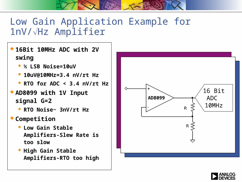
16 BitADC
10MHz
Low Gain Application Example for 1nV/Hz Amplifier
16Bit 10MHz ADC with 2V swing ½ LSB Noise=10uV 10uV@10MHz=3.4 nV/rt Hz RTO for ADC < 3.4 nV/rt Hz
AD8099 with 1V Input signal G=2 RTO Noise~ 3nV/rt Hz
Competition Low Gain Stable Amplifiers-
Slew Rate is too slow High Gain Stable Amplifiers-
RTO too high
AD8099

New Standard for High-Performance Packaging
New standard package--LFCSP
better thermals
smaller package
better parasitics
New standard pin-out is optimized for high speed
existing pin-out is 30+ years old
limits high-speed performance
better distortion
easier to lay out
bypass and feedback is optimized

New Standard LFCSP Pinout
Pin orientation is rotated by 1
Inductance coupling between
Vs and +IN is eliminated
source of second harmonic
distortion
Feedback from load is isolated
improves cap stability
1
2
3
4
8
7
6
5
–IN
–VS+IN
+VS
VOUT
CC
Feedback
Disable
+
-
NC 1
2
3
4
8
7
6
5
–IN
–VS
+IN
+VS
VOUT
CC
Disable
+
-Old Pinout
New Pinout

AD8099: Overview of Major Benefits
Enables high-speed, 16-18 bit accurate signal processing provides extra room in the error budget
Allows for use of less expensive components
less calibration/trimming
Application flexibility with wide range of gain stability designer has the advantage of low noise at low gains with high slew rate
easy to reuse in other designs
Shorter time to market, less risk and lower cost easier to lay out
less thermal modeling
lower heat budget 3mA lower quiescent current than its leading competitors


![A GENERATIVE PHONOLOGY OF SAN MATEO HUAVE Rolf …rnoyer/huave/NoyerHuaveIJAL.pdffront central back high i ɨ [+high –low] mid e o [–high –low] low a [–high +low] [–back]](https://static.documents.pub/doc/80x56/5e7d4b073e79045e90782366/a-generative-phonology-of-san-mateo-huave-rolf-rnoyerhuave-front-central-back.jpg)


