Page 1
THEORETICAL INVESTIGATION OF THERMOELECTRIC PROPERTIES OF
BULK AND NANO-SCALED SEMICONDUCTORS
BY
KYEONG HYUN PARK
THESIS
Submitted in partial fulfillment of the requirements
for the degree of Master of Science in Electrical and Computer Engineering
in the Graduate College of the
University of Illinois at Urbana-Champaign, 2012
Urbana, Illinois
Adviser:
Professor Umberto Ravaioli
Page 2
ii
Abstract
Even though thermoelectric effects have drawn more attention these days due to environmental
and economic reasons, the efficiency of the thermoelectric technology is still limited by currently
available thermoelectric materials. The priority aim in thermoelectric industry is to achieve a
higher ZT, the dimensionless thermoelectric figure of merit. There are key thermoelectric
properties determining the efficiency ZT: Seebeck coefficient, electrical conductivity, and
thermal conductivity. This work mainly focuses on strategies to obtain higher ZT and will walk
through each thermoelectric property calculation for bulk and nano-scaled semiconductors using
Landauer and phonon Boltzmann transport approaches. As a reduction of thermal conductivity in
nanoscale semiconductor wires has been reported for the last decade, scaling of semiconductor
devices changes the way heat flows through a system due to a significant increase in boundary
scattering. It will be well shown that the thermal conductivity of nanoscale semiconductors
significantly decreases compared to that of bulk semiconductors. Considering an enhancement of
ZT, a decrease in thermal conductivity is a significant issue in designing new devices while
retaining electrical conductivity. Therefore, at the end, geometrically engineered semiconductor
nanowires and superlattice nanowires will be investigated to show even more reduced phononic
transport properties compared to the straight and pure semiconductor nanowires. These results
will be expected to suggest prospective ideas to improve the current thermoelectric technology.
Page 3
iii
Contents
1. Introduction ................................................................................................................................ 1
1.1 Thermoelectric Devices ......................................................................................................... 1
1.2 Thermoelectric Effects .......................................................................................................... 2
2. Thermoelectric Transport Properties of Semiconductors .......................................................... 3
2.1 Boltzmann Transport Equation ............................................................................................. 3
2.2 Landauer Formalism ............................................................................................................. 4
2.2.1 Landauer formula ........................................................................................................... 4
2.2.2 Thermoelectric properties ............................................................................................. 5
2.2.3 Transmission function .................................................................................................... 6
2.2.4 Phonon dispersion calculation ....................................................................................... 7
3. Thermoelectric Properties of 3D and 1D Systems .................................................................... 10
3.1 Seebeck Coefficient ............................................................................................................. 10
3.2 Lattice Thermal Conductivity .............................................................................................. 11
3.3 Enhancement of ZT in 1D System ....................................................................................... 13
4. Enhanced Thermoelectric Performance ................................................................................... 15
4.1 Geometry Engineering ........................................................................................................ 15
4.1.1 Electronic transport ..................................................................................................... 15
4.1.2 Phononic transport ...................................................................................................... 16
4.1.3 Harmonic matrix setup ................................................................................................ 17
4.2 Thermal Conductivity of Superlattice Nanowires (SLNW) .................................................. 18
5. Conclusion ................................................................................................................................. 23
6. Figures ....................................................................................................................................... 24
7. Tables ........................................................................................................................................ 34
References .................................................................................................................................... 35
Page 4
1
1. Introduction
1.1 Thermoelectric Devices
Thermoelectric devices have recently captured a lot of interest in the scientific community as a
viable resource for power generation through converting waste thermal energy into electricity or
cooling systems. What makes thermoelectric devices superior to existing energy conversion
devices is the fact that they do not have any moving parts or fluids, so they are more
environmentally friendly and energy-efficient. For instance, conventional refrigerators pollute
the atmosphere due to leaking chlorofluorocarbons (CFCs) and have problems with mechanical
failure of moving parts. While current thermoelectric devices are focused on converting
electricity into heating or cooling energy, generating electricity out of wasted heat energy is
getting much more attention as the world is gradually running short of natural resources.
The efficiency of a thermoelectric system is measured through a dimensionless quantity referred
to as the thermoelectric figure of merit, which is the product of the Carnot efficiency and a
materials conversion efficiency factor:𝑍𝑇 = 𝑆2𝜍𝑇 𝜅 [1]. 𝑆 is the Seebeck coefficient, 𝜍 is
electrical conductivity, 𝑇 is the absolute temperature, and 𝜅 is thermal conductivity. The higher
the 𝑍𝑇, the more adequately electricity is generated out of the material. As the expression of 𝑍𝑇
indicates, a material with higher electrical transport properties and a lower thermal transport
property is desired to enhance the thermoelectric figure of merit. In this regard, silicon nanowire
is among the best candidates for thermoelectric applications due to the large difference in mean
free path between electrons and phonons at room temperature, the upshot of this being a reduced
thermal conductivity without affecting other electrical properties [2].
Page 5
2
1.2 Thermoelectric Effects
There are three key thermoelectric effects: the Seebeck effect, the Peltier effect, and the
Thomson effect. The Seebeck effect named for Thomas Johann Seebeck in 1821 [3], is the only
effect concerning generation of electricity as a result of a temperature gradient in thermocouples.
When heat is applied on one side of the semiconductor instead of holding it at a constant
temperature, the temperature difference forms and a certain voltage develops along the
semiconductor. This voltage is called the Seebeck voltage. Just as a current is proportional to the
applied voltage in a linear transport system with near-equilibrium condition, the voltage that
develops is expected to be proportional to the small temperature difference and the constant of
the proportionality is called the Seebeck coefficient.
While the Seebeck effect concerns electric fields produced by temperature gradients, the Peltier
effect describes the evolution or absorption of heat caused by the flow of electric current [4]. If a
positive current flows through a resistor, electrons that have random thermal motions will flow in
the opposite direction to the current and carry heat along with them since each electron has a
non-degenerate kinetic energy. As a result, the contact from which electrons carry heat away gets
cold, and the other side gets hot since the electrons dissipate the heat when they come out. This
effect is called Peltier heating or Peltier cooling [5].
Page 6
3
2. Thermoelectric Transport Properties of Semiconductors
2.1 Boltzmann Transport Equation
The thermoelectric properties mentioned above are usually obtained by solving the Boltzmann
transport equation (BTE) which is a semi-classical approach to carrier transport. The main
purpose of solving the Boltzmann equation is to find the electrical and thermal currents which
are linear functions of the electric field and temperature gradients [6].
𝐽 = 𝐿𝐸𝐸𝐸 + 𝐿𝐸𝑇∇𝑇 (1)
𝑈 = 𝐿𝑇𝐸𝐸 + 𝐿𝑇𝑇∇𝑇 (2)
The first subscripted letter of the coefficients 𝐿𝐸𝐸 , 𝐿𝐸𝑇 , 𝐿𝑇𝐸 , and 𝐿𝑇𝑇 indicates which current it
contributes to and the second letter tells which source it takes into account between the electric
field and the temperature gradients. Instead of observing these coefficients directly, two
arrangements of the apparatus enable measuring the electrical and thermal properties. In the first
setup an electric field is applied with constant temperature along the apparatus and determines
the electrical conductivity, 𝜍 = 𝐿𝐸𝐸 . In the second arrangement an open circuit prevents electric
current from flowing through the apparatus and the temperature gradient is maintained. Setting
𝐽 = 0, it gives a relation between 𝐸and ∇𝑇 , and the thermal conductivity 𝜅 , 𝑈 = −𝜅∇𝑇 , is
defined as 𝜅 = − 𝐿𝑇𝑇 −𝐿𝑇𝐸 ∙𝐿𝐸𝑇
𝐿𝐸𝐸 . Although no electrical current flows, an electric field builds
up along the device to stop the electric current flow derived by the heat flux, and this electric
field slightly reduces the thermal current [6]. The induced electric field subject to a thermal
gradient is simply expressed as 𝐸 = 𝑄∇𝑇 , and the thermopower, which is often called the
Seebeck coefficient, is 𝑆 = −𝐿𝐸𝑇 𝐿𝐸𝐸 . The coefficients are defined by combining the electric
Page 7
4
current density, the heat current density, and the solution to the BTE, and they are as follows [6]:
𝐿𝐸𝐸 = 𝑒2𝜘0, 𝐿𝐸𝑇 = −𝑒𝜘1 𝑇 = 𝐿𝑇𝐸 , and 𝐿𝑇𝑇 = −𝜘2 𝑇 , where
𝜘𝑛 = −1
3 vk
2 𝜏 𝑘 (ℇ𝑘 − 𝜁)𝑛𝜕𝑓𝑘
0
𝜕ℇ𝑘dk (3)
2.2 Landauer Formalism
2.2.1 Landauer formula
For a given voltage across its ends, a 1D channel has a finite capacity for current flow for a given
voltage across its ends. Consider that only one subband is occupied within a wire connecting two
larger reservoirs with a certain voltage difference as shown in Fig. 1. The current flowing
through the channel becomes [7]
𝐼 = ∆𝑛𝑞𝑣 =𝜌1𝑞𝑉
𝐿𝑞𝑣 =
2
ℎ𝑣𝑣𝑞2𝑉 =
2𝑞2
ℎ𝑉 (4)
where 𝜌1 is the density of states of moving carriers in reservoir 1. This relation implies that in 1D
a current depends only on the voltages and the constants by cancelling out the velocity term with
the density of states, and it produces the quantized conductance through the channel, 𝐼/𝑉 =
𝐺0 = 2𝑞2 ℎ . While this quantum conductance is valid when no scattering occurs in a wire, the
overall conductance with scattering effect is the quantum of conductance times the probability of
electron transmission through the channel ℑ(ℇ) [8]
𝐺 = (2𝑞2 ℎ )ℑ(ℇ). (5)
This equation is called the Landauer formula. For multiple channels, the total transmission
probability becomes the sum of the probabilities over the channels that contribute to electron
Page 8
5
transmission, ℑ ℇ = ℑ(ℇ)𝑖 ,𝑗 , where 𝑖, 𝑗 label the transverse eigenstates. In addition to the
multiple channels, the net current should take into account finite temperature or voltage
differences applied to the wire by multiplying the variation of Fermi-Dirac distributions of the
electrons in the left and the right, integrated over all energies.
𝐼 ℇ = 2𝑞
ℎ 𝑑ℇ[𝑓1 − 𝑓2]ℑ(ℇ)∞
−∞ (6)
When both voltage and temperature differences are applied to the system, a difference of the
Fermi distributions over all the energy levels can be simply expressed by the superposition sum
of each of the two cases.
𝑓1 − 𝑓2 ≈ −𝜕𝑓0
𝜕ℰ 𝑞∆𝑉 − −
𝜕𝑓0
𝜕ℰ
(ℰ−ℰ𝑭)
𝑇∆𝑇 (7)
2.2.2 Thermoelectric properties
Thermoelectric properties can be evaluated using the Landauer approach, and it is more effective
for low temperature applied to mesoscopic structures. In the same manner as the current density
equations (Eqs. (1) and (2)), current equations with the Landauer formalism in the linear
response regime can be expressed as a combination of electric potential and temperature
contributions with electrical transport properties [4],
𝐼 ℰ = 𝐺 ℰ ∆𝑉 − [𝑆𝐺 ℰ ]∆𝑇 (8)
𝐼𝑞 ℰ = −𝑇[𝑆𝐺 ℰ ]∆𝑉 − 𝜅0∆𝑇 (9)
Plugging in Eq. (7) into Eq. (6) gives the same form as Eq. (8) with the voltage and temperature
terms, and a comparison of these equations defines the electrical conductance, the Seebeck
coefficient, and the thermal conductance for zero electric current as [9]
Page 9
6
𝐺 ℰ = 2𝑞2
ℎ ℑ(ℇ) −
𝜕𝑓0
𝜕ℰ 𝑑ℇ
∞
−∞ (1 Ω ) (10)
𝑆 ℰ = 𝑘𝐵
−𝑞 ℑ ℇ [(ℇ−ℇ𝐹) 𝑘𝐵𝑇] −
𝜕𝑓0𝜕ℰ
𝑑ℇ∞
−∞
ℑ ℇ −𝜕𝑓0𝜕ℰ
𝑑ℇ∞
−∞
(𝑉 K ) (11)
𝜅0 = 2
ℎ𝑇 ℑ ℇ (ℇ − ℇ𝐹)2 −
𝜕𝑓0
𝜕ℰ 𝑑ℇ
∞
−∞ (𝑊 K ) (12)
where 𝑆 = 𝑆𝐺 /𝐺 and 𝜅𝑒 = 𝜅0 − 𝑇𝑆2𝐺 [10].
2.2.3 Transmission function
The transmission function ℑ(ℇ), which is an essential property that defines the current (Eq. (6))
through a conductor as well as the thermoelectric properties, is composed of the transmission
probability and the number of conducting channels, ℑ ℇ = 𝑇 ℇ 𝑀(ℇ) . The transmission
probability 𝑇 ℇ is the probability of transmission taking reflections into account. Consider that
two conductors are connected in series with transmission probability 𝑇1 and 𝑇2. See Fig. 2(a).
The total transmission cannot be simply the product of the two probabilities since multiple
transmissions from the back and forth reflections must be included [11]. Therefore, the
transmission probability is obtained by summing the probabilities of all the multiply reflected
paths as well as the direct transmissions as shown in Fig. 2(b). The total transmission probability
can be simplified using an infinite geometric expansion of the Maclaurin series since each of
both transmission and reflection probabilities is less than unity, and therefore
𝑇12 = 𝑇1𝑇2 + 𝑇1𝑇2𝑅1𝑅2 + 𝑇1𝑇2𝑅12𝑅2
2 + ⋯ = 𝑇1𝑇2
1−𝑅1𝑅2 (13)
Using a property 𝑇 = 1 − 𝑅, the transmission property with N conductors connected in series,
each having the same transmission probability, is given by 𝑇 𝑁 = 𝑇 (𝑁 1 − 𝑇 + 𝑇) , and the
Page 10
7
final expression becomes 𝑇 𝐿 = Λ
𝐿+Λ, where 𝐿 is the length of a conductor and Λ is the mean
free path, the average distance an electron can travel before it is scattered [11].
The number of conducting channels 𝑀(ℇ) , also known as density of modes, defines the
maximum conductance by counting conducting channels through which carriers transport with
the transmission probability 𝑇 ℇ [8]. A conductance with a finite cross section is ready to be
computed by obtaining the density of modes with the quantum conductance 𝐺0. Assuming that
only one parabolic subband is occupied, the density of modes for 1D, 2D, and 3D conductors is
defined by counting the number of confined subbands that can fit within the energy above the
conduction band, and they are
𝑀1𝐷 = 𝐻 𝐸 − 𝜀1 (14a)
𝑀3𝐷 = 𝐴𝑚 ∗
2𝜋ℏ2 (𝐸 − 𝐸𝐶) (14b)
where𝐻 is the unit step function, 𝜀1 is the bottom of the first subband, 𝑚∗ is the electron
effective mass, and 𝐸𝐶 is the conduction band edge. Because the density of modes is counting
modes in transverse directions, the number of conducting channels in 3D bulk conductor, 𝑀3𝐷 , is
proportional to its cross-sectional area (A), and 𝑀2𝐷 is proportional to its width (W) [9].
2.2.4 Phonon dispersion calculation
The phonon dispersion relation provides very crucial information in crystals with primitive basis
atoms. With a given polarization direction, longitudinal and transverse modes are developed for
both the acoustic and optical branches, and there are total of three times the number of atoms in
the primitive cell: three of acoustical branches and the rest of optical branches [7]. For silicon,
Page 11
8
therefore, three branches exist for each acoustic and transverse mode, and those branches consist
of one longitudinal and two transverse modes.
The phonon dispersion relation of silicon can be obtained using lattice dynamics with correct
setup of the force constants under harmonic approximation. The valence force field (VFF)
method of crystal lattice dynamics technique, which is a classical atomistic force field model, has
been used for the calculations. The VFF method takes into account several force field
interactions such as bond stretching, bond bending, torsion and inversion interactions, and
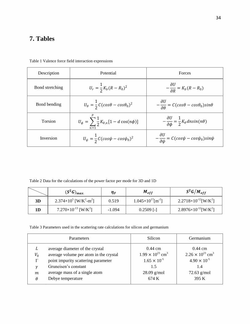
potential and force expressions for each interaction are shown in Table 1.
Those interaction equations can be adapted to the entire crystal system by applying the
interatomic potential energy in terms of the position of atoms [7]. Defining the displacement of
the atom from its equilibrium position, the Taylor expanded potential energy around its
minimum equilibrium value can be expressed as
𝑉 = 𝑉𝐸𝑄 + 1
2
𝜕2𝑉
𝜕𝑢 𝑅𝑗 𝜕𝑢 (𝑅𝑘)𝑢 𝑅𝑗 𝑢(𝑅𝑘)𝑗𝑘 + ⋯ (15)
Potential energy varies quadratically with the displacements of the atoms from their equilibrium
positions. For silicon which is classified under the diamond crystal structure, the potential energy
needs to be modified for diatomic basis, and the dynamical matrix should be set up carefully
taking care of nearest-neighbor interactions, diatomic atom interactions, and the force constants
between atoms. Once the matrix has been set, solving the dynamic equation, 𝑀𝜔2𝑢 𝑅 =
𝐷 𝑢(𝑅), for 𝜔2 simply produces an eigenvalue problem for a range of wavevectors. There are
many approaches such as adiabatic bond charge model, DFT, and linear response theory that
generate phonon dispersion relations considering not only the atomic potential but also other
Page 12
9
related crystal structures, but the lattice dynamics approach also estimates good enough acoustic
phonon dispersion relations within first Brillouin zone.
Page 13
10
3. Thermoelectric Properties of 3D and 1D Systems
3.1 Seebeck Coefficient
The Seebeck coefficient 𝑆 and the electrical conductance 𝐺 can be obtained for all dimensions
using the derived equations above, Eqs. (10) and (11). Parameters that need to be considered
with different dimensions are the number of conducting channels and the energy levels of the
first subbands because they vary with dimension. In Fig. 3, 𝑆, 𝐺, and the power factors 𝑆2𝐺 are
compared across dimensions assuming ballistic conductors with ℑ ℇ = 1, and an independent
variable is 𝜂𝐹 = (𝐸𝐹 − 𝜀1) 𝑘𝐵𝑇 , to see the behaviors of the properties with the position of Fermi
energy level, 𝐸𝐹 .
Although the magnitude of 𝑆 in 3D is greater in 3D than in 1D, they cannot be compared at the
same 𝜂𝐹 . Because their lowest subband energies are different, they are not under the same
conditions at the same 𝜂𝐹 . More importantly, the power factor 𝑆2𝐺 should be considered to see
the improvement of ZT [10]. However, concerning the units of 𝐺 in 3D containing an area term
in addition to that of 𝐺1𝐷, it is impossible to directly compare 𝑆2𝐺3𝐷 values with 𝑆2𝐺1𝐷 values.
To make the power factors comparable to each other, they need to be normalized with their own
effective density of modes defined by 𝑀𝑒𝑓𝑓 = 𝑀 𝐸 −𝜕𝑓0
𝜕𝐸 𝑑𝐸, and the power factors per
mode 𝑆2𝐺 𝑀𝑒𝑓𝑓 for each dimension are established in Table 2. The maximum 𝑆2𝐺 𝑀𝑒𝑓𝑓
increases in 1D over 3D which implies that the modes are more effectively used in 1D than in 3D.
Page 14
11
3.2 Lattice Thermal Conductivity
Lattice thermal conductivity of a solid is defined with respect to the steady-state flow of heat
along a conductor with a temperature gradient, 𝑗𝑈 = −𝜅 𝑑𝑇 𝑑𝑥 , where 𝑗𝑈 is the flux of thermal
energy. From elementary kinetic theory, the thermal conductivity is expressed by Debye [7] as
𝜅𝑙 = 1
3𝐶𝜈ℓ , with 𝐶 as the heat capacity per unit volume, 𝜈 the average phonon velocity, and ℓ
the phonon mean free path. The heat capacity from the Debye model can be defined with the
relaxation time approximation as [12]
𝐶 =3𝑉ℏ2
2𝜋2𝑣3𝑘𝐵𝑇2 𝑑𝜔
𝜔4𝑒ℏ𝜔 𝑘𝐵𝑇
(𝑒ℏ𝜔 𝑘𝐵𝑇 )2
𝜔𝐷
0= 9𝑘𝐵
𝑁
𝑉
𝑇
𝜃𝐷
3
𝑥4𝑒𝑥𝑑𝑥
𝑒𝑥−1 2
𝜃𝐷𝑇
0 (16)
where 𝑘𝐵 is Boltzmann’s constant, 𝜃𝐷 is Debye temperature, 𝑉 is the unit volume, 𝜔 is phonon
frequency, and 𝑥 = ℏ𝜔
𝑘𝐵𝑇. At low temperatures, acoustic phonons are normally excited, so the
Debye model is more appropriate for approximating the heat capacity. However, it is not valid
for phonons with high frequencies because the Debye model assumes a linear dispersion, which
is not around the boundary of the first Brillouin zone and is therefore completely wrong for
optical phonons. More appropriate at higher temperatures and higher frequencies is the Einstein
model, which assumes that all phonons have the same frequency. Although electrons also
contribute to the specific heat, this contribution is typically much smaller than the phonon heat
capacity and so has little effect on the total thermal conductivity.
In [13], the Debye model calculating the lattice thermal conductivity has been modified by
assuming that the phonon scattering processes can be represented by relaxation times which are
functions of frequency and temperature with the Planck distribution function. The model deals
with boundary scattering, normal three-phonon processes, isotope scattering, and umklapp
Page 15
12
scattering, and the normal process has a comparably small effect on the thermal conductivity at
low temperatures [13]. The lattice thermal conductivity interpreted using Callaway’s formalism
looks like [14]
𝜅𝑙,𝐵𝑢𝑙𝑘 = 𝑘𝐵
2𝜋2𝜈 𝑘𝐵𝑇
ℏ
3
𝜏𝐶(𝑥,𝑇)𝑥4𝑒𝑥𝑑𝑥
𝑒𝑥−1 2
𝜃𝐷𝑇
0 (17)
where 𝜏𝐶 is a combined relaxation time which is thus taken as 𝜏𝐶−1 = 𝜏𝐵
−1 + 𝜏𝐼−1 + 𝜏𝑈
−1, where
the right-hand-side terms are relaxation times for boundary, isotope, and umklapp scattering of
the phonons, respectively. The result of the calculation for silicon is shown in Fig. 4(a) with the
experimental data by Glassbrenner.
Considering an enhancement of ZT, a decrease in thermal conductivity is a significant issue in
designing new devices. It has been known that the lattice thermal conductivity of semiconductor
nanostructures depends on dimensions when the mean free path of carriers is comparable to the
device dimensions [15]. For the case of nanowires, the phonon boundary scattering is expected to
be the most dominant scattering mechanism. This can be confirmed by comparing the phonon
mean free path of nanowires with varying width or diameter of the cross section [16]. In this
regard, the lattice thermal conductivity for nanowires has to take spatial confinement into
account, and the equation for 𝜅𝑙 ,𝑁𝑊 can be derived by modifying the relaxation term in Eq. (17)
[15].
𝜅𝑙,𝑁𝑊 = 𝑘𝐵
2𝜋2 𝑘𝐵𝑇
ℏ
3
𝜏𝐶(𝑥 ,𝑇)
𝜈 𝑆[𝛾 𝑥 , 𝜖]
𝑥4𝑒𝑥𝑑𝑥
𝑒𝑥−1 2
𝜃𝐷𝑇
0 (18)
where 𝛾 𝑥 = [𝑤 Λ(𝑥)] is the reduced side length of a square cross section, 𝑤 is the width of the
cross section, Λ(𝑥) is the phonon mean free path, 𝜈 is the averaged phonon group velocity, and
𝑆 is a complicated function related to the boundary scattering with 𝜖 the fraction of scattered
carriers at the boundary. The averaged group velocity 𝜈 is determined by the functional
Page 16
13
dependence of the phonon group velocity on phonon energy. Using dispersion relations for
confined phonons in nanowires, the averaged group velocity is calculated over all contributing
branches [17]. Figure 4(b) shows the lattice thermal conductivities of silicon nanowires with
varying width. Compared to the lattice thermal conductivity of bulk silicon, the nanowires show
significant decreases in thermal conductivity, and a decrease in 𝜅𝑙 ,𝑁𝑊 with reduced width 𝑤
because of a decrease in relaxation time 𝜏𝐶 caused by significantly increasing the boundary
scattering.
3.3 Enhancement of ZT in 1D System
Based on the above calculations of the power factors and the thermal conductivities of bulk and
nano-scaled silicon, the thermoelectric figure of merits can be obtained. First it is necessary to
compute all the properties for the same independent variable, and Fig. 5 regenerates the Seebeck
coefficients and the power factors per mode in 3D and 1D with varying temperatures. Unlike the
plot of 𝑆 versus 𝜂𝐹 in Fig. 3(a), the temperature dependent 𝑆 in 1D is obviously greater than 𝑆 in
3D, and so is the temperature dependent 𝑆2𝐺 per mode in 1D.
With the lattice thermal conductivities calculated in the previous section, ZT in 3D and 1D are
calculated. Because the electrical conductance 𝐺 used in this calculation has already been
normalized by the effective density of modes 𝑀𝑒𝑓𝑓 , it can replace the electrical conductivity 𝜍.
The temperature dependent ZT of bulk silicon and 22 nm wide nanowire investigated in this
study are plotted in Fig. 6 along with other experimental and theoretical data from the published
papers [2,17,19]. In the range around 300K, ZT of the 22nm nanowire varies from 0.3 to 0.43
while that of the bulk silicon is below 0.1. Although the ZT values theoretically obtained in this
work seem not to match very well with the data from the previous works, the great improvement
Page 17
14
of ZT in lower dimensional semiconductor is the remarkable feature. This enhancement mostly
comes from the reduced thermal conductivity in 1D since the variation of the power factor from
3D to 1D is smaller than that of the thermal conductivity.
Page 18
15
4. Enhanced Thermoelectric Performance
4.1 Geometry Engineering
A great enhancement of ZT in ultra-small-scale semiconductor has been reported in the
foregoing. We can achieve even higher ZT through an approach called electron-crystal, phonon-
glass. Semiconductor nanowires with nano-engineered geometries are expected to draw more
efficient phonon-surface scattering as the diameter is reduced to below 50 nm [21,22]. The
corresponding drop in thermal conductivity may provide an enhancement of ZT if the electronic
transport is not as affected by surface scattering. Previous work by Martin [21,24] suggests the
enhancement of the figure of merit through interactions of the carriers with repetitive patterns at
the wire boundaries. In this work, sinusoidal wires (SineNW) are considered, as schematically
depicted in Fig. 7(a), which may be candidates to realize a phonon blockade as discussed in [23]
without degrading appreciably the electronic current.
4.1.1 Electronic transport
Solutions of electronic quantum transmission for silicon bars with sinusoidal undulations are
shown in Fig. 7(b), including a comparison with straight bars of the same cross-section. The
transmission coefficient, which represents the number of modes contributing to transmission in a
straight and smooth wire, is directly proportional to the wire resistivity due to the scattering
mechanism. The 3D conduction channel is modeled by a 1D tight binding chain, and the
quantum nature is accounted for by solving the Schrödinger equation for each cross section in
the transverse direction [6]. Different cross sections can be readily included in the model. Silicon
nanowires with length of 30 nm and cross sectional width of 6 nm and 10 nm are considered,
with several numbers of undulation peaks (N) and heights (H). N and H define the shape of
Page 19
16
undulation within the fixed length (L) by changing periods of undulation. The nanowire
undulations directly affect the resistivity particularly at higher carrier energy. However, for the
narrower wire, one can see that increasing the number of undulations only decreases the
transmission coefficient in a small way.
4.1.2 Phononic transport
The thermal conductivity of thin nanowires deviates substantially from the bulk due to phonon
blockade with a presence of boundary scattering which is dominant in mesoscopic scale devices
among the scattering mechanisms. To solve the problem of phonon transport through confined
systems, besides BTE and molecular dynamics (MD), a transmission function approach is very
well suited when phonons flow ballistically [25]. This approach enables atomistic investigation
of phonon transport through 3D nanowire systems. This work requires complex harmonic
matrices of each cross section of the targeted model, and the matrix setup procedure will be
discussed in the following section. Harmonic matrices for the system of interest and its
components to establish the harmonic relationship between any two atomic degrees of freedom
should be obtained with equilibrium atomic positions and a prescribed interatomic potential
energy model. Then, the Green’s function of the system is calculated from the pre-defined
harmonic matrices [26]. Thereafter, the net heat flow rate can be calculated from integration over
the full frequency spectrum for specified contact temperatures. Since the atomic scale system is
treated using Green’s function method, it is also called the Atomistic Green’s Function (AGF)
method [25-28]. After setting up the harmonic matrices of a nanowire constructed as shown in
Fig. 7 (a), the nanowire Green’s function and the transmission function are expressed as
G = (𝜔2I − H − Σ𝐿𝑑 − Σ𝑅
𝑑)−1 (19)
Τ 𝜔 = Tr[ ΓL G ΓL G†] (20)
Page 20
17
where H is the harmonic matrix of the nanowire and Σ𝐿𝑑 and Σ𝑅
𝑑 are the self-energy matrices of
the left and right contacts. Just like the transmission probability in the electrical conductivity
equation, Eq. (10), one can obtain heat flux through a nanowire using the transmission function
derived in Eq. (20). A great advantage of the AGF method is that any dimension or length of a
real atomic system can be handled under harmonic assumption. Actually, the dependence of
phonon transport on nanowire diameter and length was studied by Zhang et al. [27] and higher
thermal conductance with increasing cross section area and decreasing length was proved as
expected. This technique can be now benchmarked to see the phonon transport behavior through
the undulated nanowire. Real-size 3D silicon nanowires are constructed in atomic scale with
different numbers of undulation peaks and heights and used for the thermal conductance
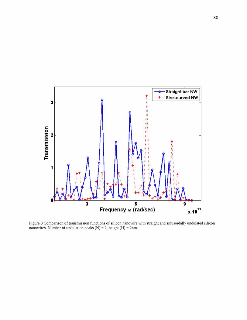
calculation. Transmission function as a function of angular frequency is shown in Fig. 8.
The sum of the transmission function of the SineNW over the whole frequency region is lower
than the straight bar NW, 19.03 compared to 28.61 respectively. This result leads to the lower
thermal conductance through the undulated than through the straight nanowires because heat flux
through a conductor is defined as a product of transmission function and phonon distribution
functions in the left and right contacts [28]. Therefore, proper geometry engineering is expected
to draw the enhancement of ZT by preventing phonon transport effectively as electronic
transport is not affected.
4.1.3 Harmonic matrix setup
Figure 9 shows a part of the FCC lattice structure, with a basis containing two identical atoms,
which is used in the lattice dynamics technique for silicon. The atoms with solid circles belong to
one FCC structure, and the atoms with the open circles are in the other.
Page 21
18
As explained in the above chapter, the VFF method is applied to the diatomic diamond lattice
structure, and the harmonic matrix discussed in the Green’s function calculation can be obtained.
The procedure is as follows. One has to define the interatomic potential between the nearest
neighbors, up to the third nearest neighbors at least, and the dynamical matrix is generated by
taking the second derivative of the potential with respect to all the displacement vectors,
𝑢11 ,𝑢12 ,𝑢13 , etc. Finding the set of eigenvalues of the dynamical matrix at different wave
vectors produces the phonon dispersion relation of the targeted model, and the dispersion relation
of silicon is displayed in Fig. 10. Solid lines are the dispersion relations with the dynamical
matrix of up to 4th
nearest neighbors, and the dotted lines are with up to 3rd
nearest neighbors.
Since only bond bending interactions of the VFF method were included in the lattice dynamics
calculation, the optical mode branches are slightly off from the experimental data, but the
acoustic mode branches which really affect the phonon transport through the device were
accurate enough to see the phonon transmission variations.
4.2 Thermal Conductivity of Superlattice Nanowires (SLNW)
It has been known that the lattice thermal conductivity of semiconductor nanowires depends on
dimensions when the mean free path of carriers is comparable to the device dimensions. In
addition to the predominant boundary scattering mechanism in a pure semiconductor nanowire,
interface scattering in between two different types of semiconductor segments poses significant
resistance to phonon transport in superlattice nanowires [29].
Because it is well known that the phonon density of states is dominated by acoustic phonon
modes at low temperature, especially lower than Debye temperature, in this work longitudinal
Page 22
19
acoustic (LA) and transverse acoustic (TA) phonons are considered as heat transport media.
While the Debye approximation assumes that the longitudinal and transverse polarization behave
identically for the simplicity, a more accurate result can be achieved when the heat capacity and
the sound velocity are treated as function of phonon frequency that can be defined using each LA
and TA phonon dispersion relation. To achieve an improvement of accuracy by adopting these
concepts, the heat capacity equation should be modified treating the phonon polarization
independently and using the phonon group velocity dependent on the phonon frequency. Instead
of the heat capacity equation in Eq. (16), the frequency-dependent heat capacity for LA and TA
phonon modes can be expressed as
𝐶𝐿,𝑇 = 𝑉ℏ2
2𝜋2𝑘𝐵𝑇2 𝑑𝜔𝜔4𝑒ℏ𝜔 𝑘𝐵𝑇
𝑣𝐿 ,𝑇3(𝑒ℏ𝜔 𝑘𝐵𝑇 )2
𝜔𝐿 ,𝑇
0 (21)
where 𝜔𝐿,𝑇 and 𝑣𝐿,𝑇 are LA or TA phonon cutoff frequency and group velocity, respectively. In
the same manner, the phonon mean free path ℓ expressed as a product of the phonon relaxation
time 𝜏 and the group velocity 𝑣 can be defined independently for each LA and TA phonon mode.
The combined relaxation time 𝜏𝐶 can be obtained in terms of the scattering rates of several
scattering mechanisms [14].
𝜏𝐶−1 = 𝜏𝐵
−1 + 𝜏𝐼−1 + 𝜏𝑈
−1 (22)
where 𝜏𝐵, 𝜏𝐼, and 𝜏𝑈 are the relaxation times for boundary, isotope, and umklapp scattering of
the phonons.
𝜏𝐵−1 =
𝑣
𝐿 (23)
𝜏𝐼−1 =
3𝑉0Γ𝜔4
𝜋𝑣3 (24)
Page 23
20
𝜏𝑈−1 =
ℎ𝛾2
2𝜋𝑚𝜃 𝑣2 exp −𝜃
3𝑇 𝜔2𝑇 (25)
All the parameters used in the above three scattering rate calculations for silicon and germanium
are summarized in Table 3 [14]. The frequency dependent group velocity is directly obtained
from the phonon dispersion relations of silicon and germanium generated by the VFF lattice
dynamics approach. It is a reverse process of finding group velocity at a certain wavevector:
Finding a wavevector corresponding to the frequency needed in the calculation and calculating
the slope of the acoustic phonon mode branch at the wavevector. Replacing the phonon mean
free path term with the phonon group velocity and the relaxation time enables us to express all
the components in the lattice thermal conductivity as function of the phonon frequency for each
LA and TA phonon mode. The resulting thermal conductivities of bulk silicon and germanium
are shown in Fig. 11.
Once the lattice thermal conductivity of bulk materials composing a superlattice nanowire are
obtained, the thermal conductivity for the superlattice nanowire can be modeled based on the
phonon Boltzmann transport equation with diffuse mismatch interface conditions [29]. When the
wire diameter and the segment length become smaller than the bulk phonon mean free path, the
superlattice nanowire thermal conductivity is defined by effective thermal conductivity of
composed bulk materials, and the effective thermal conductivity is obtained by a ratio of the
corresponding effective phonon mean free path to the bulk phonon mean free path.
𝑙𝐴,𝑒𝑓𝑓−1 = 𝑙𝐴
−1 + 4
3𝐿𝐴
−1 + 1
𝛼𝐴𝑑𝑤
−1 (26)
𝜅𝐴,𝑒𝑓𝑓 = 𝑙𝐴 ,𝑒𝑓𝑓
𝑙𝐴 𝜅𝐴 (27)
𝐿
𝜅𝑆𝐿=
𝐿𝐴
𝜅𝐴 ,𝑒𝑓𝑓 +
𝐿𝐵
𝜅𝐵 ,𝑒𝑓𝑓 (28)
Page 24
21
The above three equations are the effective phonon mean free path, the effective thermal
conductivity of one of the composing materials, and the final thermal conductivity for the
superlattice nanowire, respectively, where 𝐿𝐴, 𝐿𝐵 are segment lengths, 𝑑𝑤 is a wire diameter, and
𝛼𝐴 , 𝛼𝐵 are geometric factors which are set to be 1 in this work [29]. Equation (26) implies
effective phonon-scattering length of 3𝐿𝐴 4 and 𝛼𝐴𝑑𝑤 for interface and wire boundary scattering,
and thus the segment length and the wire dimensions are the critical factors that limit phonon
transport through the system.
Figure 12 (a) compares the thermal conductivity of Si/Ge superlattice nanowires with the
experimental thermal conductivity data of Si/SiGe superlattice nanowires from [18]. For two
different diameters, 58 and 83 nm, the thermal conductivities estimated in this study are slightly
higher than the experimental data, but they are pretty close to each other considering that the
model used in the experiment is Si/SiGe with Ge concentration of 5 to 10 %. Figure 12 (b) shows
temperature dependent thermal conductivity of Si/Ge superlattice nanowires, and they do not
vary much with temperature.
Figure 13 shows a dependence of the thermal conductivity on diameters at 300 K, and decreasing
diameters have a detrimental effect on the thermal conductivity. In addition, the thermal
conductivity changes more drastically in a diameter regime below 50 nm, while it shows even
more constant behavior with segment length less than 30 nm in the opposite regime.
Figure 14 displays the segment length dependent thermal conductivity of superlattice nanowires
at 300 K with varying diameters. Like the thermal conductivity behaviors with varying diameter,
thermal conductivity with varying segment length is observed to decrease with segment length
less than 50 nm, as shown in Fig. 14. Careful examination of the reductions of the thermal
Page 25
22
conductivity with the decreasing segment length and dimension shows that the segment length
variation has a more significant impact than the diameter variation. This proves that the
resistance due to the interface scattering is dominant over that due to the boundary scattering,
and that should explain how significant reduction of thermal conductivity can be achieved using
superlattice structures out of pure semiconductor structures.
Page 26
23
5. Conclusion
Thermoelectric properties of bulk (3D) silicon and nanowires (1D) were investigated in this
study. Enhancement of the thermoelectric figure of merit ZT in a low-dimensional system has
been addressed by reducing thermal conductivity due to an increase in boundary scattering
mechanism. The Landauer approach with ballistic assumption has been taken to the calculation
of the Seebeck coefficient and electrical conductivity, and normalized Seebeck coefficient and
power factor slightly improved in the 1D system which contributed to the enhancement of 𝑍𝑇.
The lattice thermal conductivity was calculated from the phonon Boltzmann transport equation in
the relaxation time approximation, and reduced thermal conductivity with decreasing cross-
section dimensions of nanowires has been confirmed. At the end of the comparison between 3D
and 1D systems, theoretically calculated ZT in 1D became a few orders of magnitude greater
than that in 3D, showing that silicon nanowires are candidates for future thermoelectric
applications. To achieve even higher ZT, thermoelectric properties of sinusoidally undulated
nanowires were investigated and resulted in a reduction of lattice thermal conductivity without
much degradation on electronic transport. In addition to the geometry engineering, thermal
conductivity of Si/Ge superlattice nanowires was calculated adopting the frequency dependent
thermal conductivity calculation technique, and the SLNW has proposed itself as a potential
candidate for the thermoelectric engineering structure. Based on the results in this work, other
applicable materials and geometries can be proposed later to test their thermoelectric
performance.
Page 27
24
6. Figures
Figure 1 A single channel between two reservoirs for an applied bias voltage difference V1-V2. The terms 𝛍𝟏 and 𝛍𝟐
are the chemical potentials on the left- and right-hand sides, respectively, and 𝐪 = −𝐞 for electrons and +𝐞 for
holes.
Figure 2 (a) Two resistors connected in series with transmission probabilities T1 and T2 and reflection probabilities
R1 and R2. (b) The net transmission through two scatterers by summing the probabilities of all reflected paths.
Page 28
25
Figure 3 Model calculation results for (a) the Seebeck coefficients, (b) the electrical conductance and power factors
in 3D and 1D, T = 300K and m* = m0.
(a)
(b)
Page 29
26
Figure 4 Comparison of the low-temperature κ results for bulk Si with ν = 9.5×105 cm/s and θ = 674 K. (b) Thermal
conductivities of nanowires with varying width. Solid lines are theoretical values calculated in this study, and
squares are experimental data taken from [18].
(a)
(b)
Page 30
27
Figure 5 𝑺 and 𝑺𝟐𝝈 through 3D and 1D conductors with varying temperature.
Page 31
28
Figure 6 ZT of bulk Si and 22nm SiNW investigated in this study and data from the published papers.
Page 32
29
Figure 7 (a) 3D Model of a silicon nanowire with sinusoidal undulation. (b) Comparison of sine-curved NWs with
straight NWs, W=6, 10nm.
(a)
(b)
Page 33
30
Figure 8 Comparison of transmission functions of silicon nanowire with straight and sinusoidally undulated silicon
nanowires. Number of undulation peaks (N) = 2, height (H) = 2nm.
Page 34
31
Figure 9 A part of the diatomic diamond lattice structure.
Figure 10 Phonon dispersion relation of silicon (solid line = 4th nearest neighbors, dotted line = 3rd nearest
neighbors).
Page 35
32
Figure 11 Lattice thermal conductivity of bulk silicon and germanium.
Figure 12 (a) Thermal conductivity of Si/Ge superlattice nanowires. (b) Temperature dependent thermal
conductivity of SLNW.
(a) (b)
Page 36
33
Figure 13 Thermal conductivity of Si/Ge superlattice nanowires with varying diameter at 300K.
Figure 14 Thermal conductivity of Si/Ge superlattice nanowires with varying segment length at 300K.
Page 37
34
7. Tables
Table 1 Valence force field interaction expressions
Description Potential Forces
Bond stretching 𝑈𝑟 =1
2𝐾𝑏(𝑅 − 𝑅0)2 −
𝜕𝑈
𝜕𝑅= 𝐾𝑏(𝑅 − 𝑅0)
Bond bending 𝑈𝜃 =1
2𝐶(𝑐𝑜𝑠𝜃 − 𝑐𝑜𝑠𝜃0)2 −
𝜕𝑈
𝜕𝜃= 𝐶(𝑐𝑜𝑠𝜃 − 𝑐𝑜𝑠𝜃0)𝑠𝑖𝑛𝜃
Torsion 𝑈𝜙 = 1
2𝐾𝜃 ,𝑛 [1 − 𝑑 cos 𝑛𝜙 ]
𝑝
𝑛=1
−𝜕𝑈
𝜕𝜙=
1
2𝐾𝜃𝑑𝑛𝑠𝑖𝑛(𝑛𝜃)
Inversion 𝑈𝜓 =1
2𝐶(𝑐𝑜𝑠𝜓 − 𝑐𝑜𝑠𝜓0)2 −
𝜕𝑈
𝜕𝜓= 𝐶(𝑐𝑜𝑠𝜓 − 𝑐𝑜𝑠𝜓0)𝑠𝑖𝑛𝜓
Table 2 Data for the calculations of the power factor per mode for 3D and 1D
(𝑺𝟐𝑮)𝒎𝒂𝒙. 𝜼𝑭 𝑴𝒆𝒇𝒇 𝑺𝟐𝑮 𝑴𝒆𝒇𝒇
3D 2.374×10⁵ [W/K
2-m
2] 0.519 1.045×10
17[m
-2] 2.2718×10
-12[W/K
2]
1D 7.270×10⁻¹³
[W/K2] -1.094 0.2509 [-] 2.8976×10
-12[W/K
2]
Table 3 Parameters used in the scattering rate calculations for silicon and germanium
Parameters Silicon Germanium
𝐿
𝑉0
Γ
𝛾
𝑚
𝜃
average diameter of the crystal
average volume per atom in the crystal
point impurity scattering parameter
Gruneisen’s constant
average mass of a single atom
Debye temperature
0.44 cm
1.99 × 10²³
cm3
1.65 × 10⁻⁵
1.5
28.09 g/mol
674 K
0.44 cm
2.26 × 10²³
cm3
4.90 × 10⁻⁵
1.4
72.63 g/mol
395 K
Page 38
35
References
[1] G. Chen, Nanoscale Energy Transport and Conversion (Oxford University Press, 2005), pp. 228-237.
[2] A. I. Hochbaum et al., “Enhanced Thermoelectric Performance of Rough Silicon Nanowires,” Nature 451,
06381 (2008).
[3] R. K. Willardson and A. C. Beer, Recent Trends in Thermoelectric Materials Research, Part One
(Semiconductors and Semimetals) Vol. 69 (Academic Press, 2000).
[4] M. Lundstrom, Fundamentals of Carrier Transport (Cambridge University Press 2nd ed, 2000), pp. 191-195.
[5] D. M. Rowe, Thermoelectrics Handbook: Macro to Nano (Taylor & Francis Group, 2006).
[6] J. M. Ziman, Electrons and Phonons: The Theory of Transport Phenomena in Solids (Oxford, 1962) pp. 264-
307.
[7] C. Kittel, Introduction to Solid State Physics (John Wiley & Sons, Inc. 8th ed, 2005).
[8] S. Datta, Quantum Transport: Atom to Transistor (Cambridge University Press, 2005).
[9] C. Jeong et al., “On Landauer vs. Boltzmann and full band vs. effective mass evaluation of thermoelectric
transport coefficients,” J. Appl. Phys. 107, 023707 (2010).
[10] R. Kim et al., “Influence of dimensionality on thermoelectric device performance,” Birck and NCN
Publications 539 (2009).
[11] S. Datta, Electronic Transport in Mesoscopic Systems (Cambridge University Press, 1st ed., 1997).
[12] G. Chen, Nanoscale Energy Transport and Conversion (Oxford University Press, 2005), pp. 147.
[13] J. Callaway, “Model for lattice thermal conductivity at low temperatures,” Phys. Rev. 113, 1046 (1959).
[14] C. J. Glassbrenner and G. A. Slack, “Thermal conductivity of silicon and germanium from 3K to the melting
point,” Phys. Rev. 134, 4A (1964).
[15] X. Lu and J. Chu, “Lattice thermal conductivity in a silicon nanowire with square cross section,” J. Appl. Phys.
100, 014305 (2006).
[16] M. Kazan et al., “Thermal conductivity of silicon bulk and nanowires: Effects of isotropic composition, phonon
confinement, and surface roughness,” J. Appl. Phys. 107, 083503 (2010).
[17] J. Zou and A. Balandin, “Phonon heat conduction in a semiconductor nanowire,” J. Appl. Phys. 89, 5 (2001).
[18] D. Li et al., “Thermal conductivity of individual silicon nanowires,” A. Phys. Lett. 83, 14 (2003).
[19] S. K. Bux et al., “Nanostructured bulk silicon as an effective thermoelectric material,” Adv. Funct. Mater. 19,
2445-2452 (2009).
[20] A. I. Boukai et al., “Silicon nanowires as efficient thermoelectric materials,” Nature 451, 06458 (2008).
[21] P. Martin et al., “Impact of phonon-surface roughness scattering on thermal conductivity of thin silicon
nanowires,” PRL 102, 125503 (2009).
[22] M. Soini et al., “Thermal conductivity of GaAs nanowires studied by micro-Raman spectroscopy combined
with laser heating,” Appl. Phys. Lett, 97, 263107 (2010).
[23] P. Martin and U. Ravaioli, “Green function treatment of electronic transport in narrow rough semiconductor
conduction channels,” J. Phys.: Conference Series 193, 012009 (2009).
[24] J.-S. Héron et al., “Phonon transport in structured silicon nanowire,” available online at
http://www.em2c.ecp.fr/TRN07/Heron_TRN07.pdf (2007).
Page 39
36
[25] N. Mingo et al., “Phonon transport in nanowires coated with an amorphous material: An atomistic Green’s
function approach,” Phys. Rev. B 68, 245406 (2003).
[26] P. E. Hopkins et al., “Extracting phonon thermal conductance across atomic junctions: Nonequilibrium Green’s
function approach compared to semiclassical methods,” J. Appl. Phys. 106, 063503 (2009).
[27] W. Zhang et al., “Simulation of phonon transport across a non-polar nanowire junction using an atomistic
Green’s function method,” Phys. Rev. B 76, 195429 (2007).
[28] W. Zhang et al., “The atomistic green’s function method: An efficient simulation approach for nanoscale
phonon transport,” Heat Transfer, Part B, 51: 333-349 (2007).
[29] Y. Lin and M. S. Dresselhaus, “Thermoelectric properties of superlattice nanowires,” Phys. Rev. B 68, 075304 (2003).