Outline Optical Transitions Optical Spectroscopy Excitons, Defects and Symmetry Effects Theory and Application of Nanomaterials Lecture 8: Optical Spectroscopy S. Smith SDSMT, Nano SE FA17: 8/25-12/8/17 S. Smith (SDSMT, Nano SE) Theory and Application of Nanomaterials FA17: 8/25-12/8/17 1 / 20
Transcript
Outline Optical Transitions Optical Spectroscopy Excitons, Defects and Symmetry Effects
Theory and Application of NanomaterialsLecture 8: Optical Spectroscopy
S. Smith
SDSMT, Nano SE
FA17: 8/25-12/8/17
S. Smith (SDSMT, Nano SE) Theory and Application of Nanomaterials FA17: 8/25-12/8/17 1 / 20
Outline Optical Transitions Optical Spectroscopy Excitons, Defects and Symmetry Effects
Introduction
Interaction of light with matter can reveal details about electronic transitions describedby quantum mechanics. One need is to probe ever-smaller volumes of materials, e.g.nano-materials. Below, a Micro-spectroscopy method is employed to look at sub micronfeatures at varying temperatures.
Figure: A micro-spectroscopy set-up capable of examining sub-micron regions ofmaterials at temperatures down to 4K. The solid immersion lens sits on the samplesurface, and enhances the resolution of the far-field objective by increasing the refractiveindex.
S. Smith (SDSMT, Nano SE) Theory and Application of Nanomaterials FA17: 8/25-12/8/17 2 / 20
Outline Optical Transitions Optical Spectroscopy Excitons, Defects and Symmetry Effects
Outline
1 Optical TransitionsLight ScatteringSelection RulesEnergy Relaxation or ‘Carrier Cooling’
2 Optical SpectroscopyMeasuring Emission (Fluorescence/Luminescence)Measuring Absorption (PLE)Time Resolved LuminescenceInterpretation of Time Resolved LuminescenceUltrafast Transient Absorption
3 Excitons, Defects and Symmetry EffectsExcitonsDonor Acceptor PairsValence Band Splitting
S. Smith (SDSMT, Nano SE) Theory and Application of Nanomaterials FA17: 8/25-12/8/17 3 / 20
Outline Optical Transitions Optical Spectroscopy Excitons, Defects and Symmetry Effects
Light Scattering
Due to electron-photon coupling, energy and momentum can be exchanged with matter viainteraction with electromagnetic radiation. Energy and momentum conservation require:
E2 − E1 = hν −→ Energy conserved
~k2 − ~k1 = ~kp −→ Momentum conserved
Figure: A Feyman diagram describing the evolution of an optical transition wherein an electronof energy E1 and momentum k1 absorbs a photon of energy hν and momentum ~kp . Time axisis by convention implied from left to right, but shown here explicitly.
S. Smith (SDSMT, Nano SE) Theory and Application of Nanomaterials FA17: 8/25-12/8/17 4 / 20
Outline Optical Transitions Optical Spectroscopy Excitons, Defects and Symmetry Effects
Emission Processes
Below are shown to emission processes involving emission of light by change of electronenergy level (fluorescence or luminescence) and by inelastic scattering of light of latticevibrations or phonons (Raman scattering).
Figure: Feyman diagrams describing the evolution of an electron transition wherein anelectron of energy E1 and momentum k1 emits a photon of energy E = hν = E1 − E2
and momentum ~kp = ~(k1 − k2) (above) or phonon of energy ~Ω and momentum~kph(below).
S. Smith (SDSMT, Nano SE) Theory and Application of Nanomaterials FA17: 8/25-12/8/17 5 / 20
Outline Optical Transitions Optical Spectroscopy Excitons, Defects and Symmetry Effects
Optical Transitions
Having computed the wave function, we wish to describe general properties ofoptically-induced transitions. We will assume the wave function has the general form:
|ψ〉 = | n, l ,ml︸ ︷︷ ︸spatial
; s︸︷︷︸spin
〉
In general, a transition will involve a change of quantum state, for instance between twoEigenstates here represented as atomic levels:
Figure: Energy level diagram showing an absorption of a photon of energy hν, resultingin an atomic transition between to quantum states.
S. Smith (SDSMT, Nano SE) Theory and Application of Nanomaterials FA17: 8/25-12/8/17 6 / 20
Outline Optical Transitions Optical Spectroscopy Excitons, Defects and Symmetry Effects
Selection Rules
The transition rate is given by Fermi’s golden rule:
Wfi =2π
~|〈n, l ,ml , s|Hint(0)|no , lo ,mlo , so〉|2δ(∆Enno − ~ω)
as we saw in our previous discussion of quantum mechanics and transitions betweenquantum states. Evaluating the expression for the matrix element, we can quote someselection rules:
〈ψf |Hint |ψi 〉 = 〈sf |si 〉〈n, l ,ml |Hint(0)|no , lo ,mlo 〉〈sf |si 〉 = δif spin allowed for i = f
〈n, l ,ml |Hint(0)|no , lo ,mlo 〉 6= 0 dipole allowed
Where the spin dependent part of the wave function is independent of the spatialcoordinates and we can therefore factor the expression out. We say the transition is spinallowed if the spin portion of the matrix element is non-zero, and, since we usedHint = −p · E to calculate the matrix element (see discussion of Fermi’s golden rule), ifthe spatial portion of the matrix element is non-zero we say the transition is dipoleallowed.
S. Smith (SDSMT, Nano SE) Theory and Application of Nanomaterials FA17: 8/25-12/8/17 7 / 20
Outline Optical Transitions Optical Spectroscopy Excitons, Defects and Symmetry Effects
Energy Relaxation in Solids
Figure: (left): Band filling in extended zone scheme. (right): Scattering diagramshowing the processes which lead to light emission from a semiconductor: light absorbedat E = hν ≥ Eg . Excess energy is lost by rapid phonon emission and emission at energyE = hν ≈ Eg .
S. Smith (SDSMT, Nano SE) Theory and Application of Nanomaterials FA17: 8/25-12/8/17 8 / 20
Outline Optical Transitions Optical Spectroscopy Excitons, Defects and Symmetry Effects
Energy Relaxation in Molecules
A similar mechanism in molecules is depicted in figure 6, the conduction and valencebands are now replaced with their molecular counterparts, the so-called LUMO (lowestunoccupied molecular orbital) and HOMO (highest occupied molecular orbital) energylevels. The molecular counterpart to the phonons in crystals are the normal modes ofvibration of the molecule, with discrete energies.
Figure: An energy level diagram describing the absorption and emission of a photon in amolecule. Note the energy of the emitted photon is less than the absorbed photon dueto internal energy relaxation.
S. Smith (SDSMT, Nano SE) Theory and Application of Nanomaterials FA17: 8/25-12/8/17 9 / 20
Outline Optical Transitions Optical Spectroscopy Excitons, Defects and Symmetry Effects
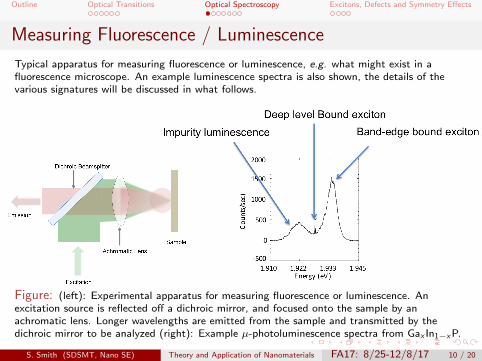
Measuring Fluorescence / Luminescence
Typical apparatus for measuring fluorescence or luminescence, e.g. what might exist in afluorescence microscope. An example luminescence spectra is also shown, the details of thevarious signatures will be discussed in what follows.
Figure: (left): Experimental apparatus for measuring fluorescence or luminescence. Anexcitation source is reflected off a dichroic mirror, and focused onto the sample by anachromatic lens. Longer wavelengths are emitted from the sample and transmitted by thedichroic mirror to be analyzed (right): Example µ-photoluminescence spectra from Gax In1−x P.
S. Smith (SDSMT, Nano SE) Theory and Application of Nanomaterials FA17: 8/25-12/8/17 10 / 20
Outline Optical Transitions Optical Spectroscopy Excitons, Defects and Symmetry Effects
Density of States
In the figure below, the parabolic band approximation for a type-I semiconductor (e.g. GaAs) isshown. Plotted alongside the dispersion relation is the density of states (DOS). The DOS, orρc(v)(E), is dependent on the volume of a shell in k-space, and will be zero at the gaps, thus theshape of ρc(v)(E) should be similar to what is sketched.
Figure: The density of states (DOS), or ρc/v (E), is shown alongside the energy dispersionrelation in the parabolic band approximation for a direct-gap semiconductor.
S. Smith (SDSMT, Nano SE) Theory and Application of Nanomaterials FA17: 8/25-12/8/17 11 / 20
Outline Optical Transitions Optical Spectroscopy Excitons, Defects and Symmetry Effects
The principle of Photoluminescence excitation spectroscopy, or PLE, is based on energyrelaxation, which results in emission at a lower energy than absorption. In the left part of thefigure, an emission spectra is shown, centered around an energy Eg − Eb, if a spectrometer canbe set to an energy below this, a laser excitation source (whose energy range is represented bythe green arrow in the figure) can be scanned continuously towards higher energy.
Figure: (Left): A photoluminescence (PL) spectra resulting from excitonic recombination, anarrow energy range near the low energy tail of the spectra is selected as the PLE detectionenergy. The green arrow shows the range of excitation energies which will be used to obtain thePLE spectra. (Right): Photoluminescence intensity at the PLE detection energy plotted as afunction of excitation energy is proportional to the density of states ρ(E).
S. Smith (SDSMT, Nano SE) Theory and Application of Nanomaterials FA17: 8/25-12/8/17 12 / 20
Outline Optical Transitions Optical Spectroscopy Excitons, Defects and Symmetry Effects
Measuring Time Resolved Photo-Luminescence (TRPL)
The most basic time-dependent measurement is time-resolved PL or TRPL, a proto-typicalexample is shown below. The measurement can be made using a number of methods, includingtime-correlated single photon counting (TCSPC) with a time-resolution on the order of 500ps,or using a streak-camera, with a resolution in the sub-picosecond range.
Figure: (Left): Photo-luminescence, or PL, is initiated by an excitation pulse (blue), andtime-resolved to show the recombination as function of time (red). (Right): A typical decaytrace will be dominated by the recombination lifetime, but in principle is influenced by carrierthermalization, which takes place on a timescale typically very short compared to recombination.
S. Smith (SDSMT, Nano SE) Theory and Application of Nanomaterials FA17: 8/25-12/8/17 13 / 20
Outline Optical Transitions Optical Spectroscopy Excitons, Defects and Symmetry Effects
Interpreting Time Resolved Photo-Luminescence (TRPL)
The measured fluorescence or luminescence decay time can often becharacterized by a single exponential decay, e.g.:
I (t) = Ioe−t/τ
but the decay rate τ may have other contributions beyond the radiativedecay rate based on the quantum transition rate, which are usuallysub-divided into radiative and non-radiative components, related as so:
1
τ=
1
τR
+1
τNR
where the possibility that a transition which does not involve emitting aphoton may contribute to the observed decay τ . For instance, phononemission where the optical energy of the photon is converted to heat.
S. Smith (SDSMT, Nano SE) Theory and Application of Nanomaterials FA17: 8/25-12/8/17 14 / 20
Outline Optical Transitions Optical Spectroscopy Excitons, Defects and Symmetry Effects
Transport contributions to recombination
Mobile carriers (electrons and holes) can freely diffuse, and therefore the recombination rate willdepend on the probability that two carriers of opposite type (electron/hole) will occupy thesame site in the crystal.
Figure: In a system where the excited state is mobile, such as a semiconductor ormolecular crystal, transport effects influence the measured recombination rate orfluorescence / luminescence decay.
S. Smith (SDSMT, Nano SE) Theory and Application of Nanomaterials FA17: 8/25-12/8/17 15 / 20
Outline Optical Transitions Optical Spectroscopy Excitons, Defects and Symmetry Effects
Ultrafast Transient Absorption
For optically thin samples, differential transmission, also known as transient absorption, is awell-known method which measures directly the changes in absorption on a femtosecond timescale. An intense “pump” pulse fills some fraction of the available states, resulting in increasedtransmission (reduced absorption) which will be dependent on the choice of time delay τbetween the “pump” and “probe” pulse.
Figure: (Left): Differential transmission utilizes an intense pump pulse and typically a lessintense probe pulse, delayed by a time τ . Transmission is then a function of time delay τ due tostate-filling effects. (Right): Typically the differential transmission, ∆T/T (τ) is plotted vs.delay τ . Illustrating the ultrafast hot carrier cooling and slower recombination processes forτ τc , the carrier cooling rate.
S. Smith (SDSMT, Nano SE) Theory and Application of Nanomaterials FA17: 8/25-12/8/17 16 / 20
Outline Optical Transitions Optical Spectroscopy Excitons, Defects and Symmetry Effects
Excitons
An electron in a conducting state may be bound to the positively charged hole, and thecentro-symmetric system forms a so-called “quasi-particle” known as an exciton. Thecoulomb attraction between the electron and hole results in a binding energy:
Eb =m∗q4
2h2c2
1
n2=
13.6eV
(ε/εo)2
m∗
mo
1
n2
quantum number n, which specifies the s-wave character exciton states.
Ebind ∼ 10meV in GaAs, < kBT at room temperature (23meV).
Integral spin, due to the combination of electron and hole spin, behaving as aBoson, thus Excitons are candidates for Bose-Einstein condensation.
Figure: Schematic of quasi-particle referred to as an Exciton – an electron-hole pairbound together in an orbital system by coulomb attraction.
S. Smith (SDSMT, Nano SE) Theory and Application of Nanomaterials FA17: 8/25-12/8/17 17 / 20
Outline Optical Transitions Optical Spectroscopy Excitons, Defects and Symmetry Effects
Impurties in Semiconductors
An impurity in a perfect crystal breaks the translational symmetry and creates alocalized defect state. The impurity can either give up a charge (donor) which istransferred into one of the Bloch states of the crystal, or take up a charge (acceptor).The carrier concentration due to the presence of these impurities can be calculated fromstatistical physics, for instance the carrier concentration due to the density Nd donors is:
n ∼= (noNd )1/2e−Ed/2kB
T where no = 2(mekBT/2π~2)3/2
These levels can also trap excitons, and as a result, below-gap emission can occur, asseen in the figure below.
Figure: Energy level diagram showing donor and acceptor levels and recombination for donoracceptor pairs.
S. Smith (SDSMT, Nano SE) Theory and Application of Nanomaterials FA17: 8/25-12/8/17 18 / 20
Outline Optical Transitions Optical Spectroscopy Excitons, Defects and Symmetry Effects
Donor Acceptor Pairs
The energy of this emission is observed in discrete lines, corresponding to integralnumbers of lattice spacings, for which the coulomb attraction varies discretely, resultingin a series of lines corresponding to varying donor-acceptor separation are observed:
Figure: Donor-acceptor emission is modulated by discrete fluctuations in the nearestneighbor distance, which modulate the coulomb interaction energy.
S. Smith (SDSMT, Nano SE) Theory and Application of Nanomaterials FA17: 8/25-12/8/17 19 / 20
Outline Optical Transitions Optical Spectroscopy Excitons, Defects and Symmetry Effects
Valence Band Splitting
One notes the varying curvature of the bands in the figure, and this is described in terms of the“effective mass”, derived from the curvature of the energy dispersion relation:
E =~2k2
2m−→
1
m∗ =1
~2
d2E
dk2
Based on the curvature, the two degenerate bands at the valence band maxima are labelled“heavy” and “light” hole bands (designated hh and lh), an additional band due to the spin-orbitinteraction is also shown:
Figure: Parabolic band approximation for typical direct gap semiconductor, showingdegeneracy in valence band at k = 0, so-called heavy and light hole bands and split-off band.
S. Smith (SDSMT, Nano SE) Theory and Application of Nanomaterials FA17: 8/25-12/8/17 20 / 20