Theory of electron-phonon interactions on nanoscales: semiconductor surfaces and two dimensional electron gases N. Buecking a , S. Butscher a , M. Richter a , C. Weber b , S. Declair a , M. Woerner c , K. Reimann c , P. Kratzer d , M. Scheffler e and A. Knorr a a Institut f¨ ur Theoretische Physik, Nichtlineare Optik und Quantenelektronik, Technische Universit¨ at Berlin, Hardenbergstr. 36, 10623 Berlin, Germany b Mathematical Physics, Lund University, Box 118, 22100 Lund, Sweden c Max Born Institut f¨ ur Nichtlineare Optik und Kurzzeitspektroskopie, Max-Born-Straße 2A, 12489 Berlin, Germany d Theoretische Physik, Universit¨at Duisburg-Essen, Lotharstr. 1, 47048 Duisburg, Germany e Fritz-Haber-Institut der Max-Planck-Gesellschaft, Faradayweg 4-6, 14195 Berlin, Germany ABSTRACT A theory of electron relaxation for electron gases in semiconductor quantum well structures and at semiconductor surfaces is presented. The electron relaxation is described by quantum-kinetic equations. In the nonlinear optical response of a two dimensional electron gas in a GaN quantum well, polaronic signatures are clearly enhanced compared to the linear response, if the pump pulse is tuned to the polaron energy. For the phonon-induced electron relaxation at Si (001) surface structures, the interplay of bulk and surface states yields a complex temporal relaxation dynamics depending on the slab thickness. 1. OUTLINE After introducing the theoretical formalism for the underlying density matrix theory, we calculate in this paper the linear and nonlinear optical response of higher order electron-phonon interaction in ISB transitions in a GaN quantum well (QW) within a Bloch equation approach 1 using a correlation expansion 2, 3 beyond the second order Born approximation. By generalizing such an approach beyond a single band problem, 4 our approach is able to qualitatively reproduce experimental results for doped gallium nitride quantum wells 5, 6 in the linear and the nonlinear regime. In the last part of this paper, we investigate the relaxation dynamics at a silicon surface 7, 8 after optical excitation. After performing density-functional-theory calculations for the Si (001) 2 × 1 surface, density matrix equations in the second order born limit are used to compute the evolution of the population of the conduction bands. 9, 10 2. THEORY OF THE ELECTRON-PHONON INTERACTION Many-particle effects are of fundamental importance for the optical properties of two dimensionally quantum confined electrons in nanostructured semiconductors. Examples constitute finite free standing semiconductor slabs 9–12 as well as the ideal two dimensional electron gas (2DEG) in doped quantum wells. 13 The Hamilton operators of the free phonons and electrons, the electron-field interaction in dipole approximation and for the electron-phonon interaction are: 2, 9 H 0 = nk ε nk a † nk a nk + iq ¯ hω iq b † iq b iq , H field = kn=n A(t)p n k nk a † nk a n k , H EPI = nk n k iq g n k nk iq a † nk a n k b iq + h.a.. (1) Invited Paper Ultrafast Phenomena in Semiconductors and Nanostructure Materials XII edited by Jin-Joo Song, Kong-Thon Tsen, Markus Betz, Abdulhakem Y. Elezzabi Proc. of SPIE Vol. 6892, 689209, (2008) · 0277-786X/08/$18 · doi: 10.1117/12.768659 Proc. of SPIE Vol. 6892 689209-1
Transcript
Theory of electron-phonon interactions on nanoscales:semiconductor surfaces and two dimensional electron gases
N. Bueckinga, S. Butschera, M. Richtera, C. Weberb, S. Declaira, M. Woernerc, K. Reimannc,P. Kratzerd, M. Schefflere and A. Knorra
eFritz-Haber-Institut der Max-Planck-Gesellschaft, Faradayweg 4-6, 14195 Berlin, Germany
ABSTRACT
A theory of electron relaxation for electron gases in semiconductor quantum well structures and at semiconductorsurfaces is presented. The electron relaxation is described by quantum-kinetic equations. In the nonlinear opticalresponse of a two dimensional electron gas in a GaN quantum well, polaronic signatures are clearly enhancedcompared to the linear response, if the pump pulse is tuned to the polaron energy. For the phonon-inducedelectron relaxation at Si (001) surface structures, the interplay of bulk and surface states yields a complextemporal relaxation dynamics depending on the slab thickness.
1. OUTLINE
After introducing the theoretical formalism for the underlying density matrix theory, we calculate in this paperthe linear and nonlinear optical response of higher order electron-phonon interaction in ISB transitions in a GaNquantum well (QW) within a Bloch equation approach1 using a correlation expansion2, 3 beyond the second orderBorn approximation. By generalizing such an approach beyond a single band problem,4 our approach is ableto qualitatively reproduce experimental results for doped gallium nitride quantum wells5, 6 in the linear and thenonlinear regime. In the last part of this paper, we investigate the relaxation dynamics at a silicon surface7, 8
after optical excitation. After performing density-functional-theory calculations for the Si (001) 2 × 1 surface,density matrix equations in the second order born limit are used to compute the evolution of the population ofthe conduction bands.9, 10
2. THEORY OF THE ELECTRON-PHONON INTERACTION
Many-particle effects are of fundamental importance for the optical properties of two dimensionally quantumconfined electrons in nanostructured semiconductors. Examples constitute finite free standing semiconductorslabs9–12 as well as the ideal two dimensional electron gas (2DEG) in doped quantum wells.13 The Hamiltonoperators of the free phonons and electrons, the electron-field interaction in dipole approximation and for theelectron-phonon interaction are:2, 9
H0 =∑
nk
εnka†nkank +
∑
iq
hωiqb†iqbiq, Hfield =∑
kn�=n′A(t)pn′k
nk a†nkan′k,
HEPI =∑
nkn′k′iq
gn′k′nkiq
a†nkan′k′biq + h.a.. (1)
Invited Paper
Ultrafast Phenomena in Semiconductors and Nanostructure Materials XII edited by Jin-Joo Song, Kong-Thon Tsen, Markus Betz, Abdulhakem Y. Elezzabi
Proc. of SPIE Vol. 6892, 689209, (2008) · 0277-786X/08/$18 · doi: 10.1117/12.768659
Proc. of SPIE Vol. 6892 689209-1
1
2ε(k)
k
aml
am’l’+
biq+
ank
an’k+
relaxation (phonon creation)opticalexcitation
Figure 1. Schematic diagram of the band structures and possible optical transitions. On the lhs, the left arrow indicatesa single particle transition in a doped quantum well, where the lowest conduction subband is occupied. The right arrowindicates a transition via a virtual level, combined with a phonon emission process. On the rhs, excitation and electronrelaxation in multiband-structure (band dispersion parallel to the surface) is illustrated.
Here, a†mk, amk and b†iq, biq are creation and annihilation operators for electrons with wave vector k in (sub)band
m and for phonons of mode i with wave vector q (q|| is its in-plane projection). εlk is the free energy of an electronin (sub)band l with wavevector k and ωiq the phonon frequency of a phonon in mode i at wave vector q. Withthese operators, we can express coherences pml
nk := 〈a†nkaml〉, (sub)band occupations fnk := 〈a†
nkank〉, and thephonon occupation numbers niq = 〈b†iqbiq〉. gn′k′
nk,iq denotes the electron-phonon coupling matrix elements, pmknk
is the momentum matrix element between (sub)band n and m, and A(t) the external electric vector potentialdescribing the applied optical field.
Using the Heisenberg equation of motion we can find equations of motion (EOM) for the coherence and thephonon assisted density matrices sm′l′
ml,iq = 〈a†mlam′l′biq〉:9
ihd
dtpm′l′
ml =(εml − εm′l′
)pm′l′
ml + A(t)∑
nk
(pnk
mlpm′l′nk − pm′l′
nk pnkml
)(2a)
+∑
nkiq
(gnk
mliq
(snk
m′l′iq
)∗+ gnk
mliq
sm′l′ankiq
− gm′l′nkiq
(sml
nkiq
)∗− gm′l′
nkiq
snkmliq
)
and
ihd
dt
(sml
m′l′iq
)∗ =(εml − εm′l′ + hωiq
)(sml
m′l′iq
)∗ + A(t)∑
nk
(pnk
ml
(snk
m′l′iq
)∗ − pm′l′nk
(sml
nkiq
)∗)
+∑
nki′q′
(gnk
mli′q′
(R
m′l′i′q′nkiq
)∗+ gnk
mli′q′
Tm′l′i′q′nkiq
− gm′l′nki′q′
(R
nki′q′mliq
)∗− gm′l′
nki′q′
Tnk′i′q′mliq
)
+∑
nkn′k′
gn′k′nkiq
〈a†mla
†nkam′l′an′k′〉, (2b)
where Rml,i′q′nk,iq = 〈a†
nkamlbiqbi′q′〉 and T ml,i′q′nk,iq = 〈a†
nkamlb†iqbi′q′〉. Through the electron-phonon interaction, the
resulting equations of motion9, 14, 15 (Eqs. (2a), (2b)) of the single particle density matrices pm′l′ml couple to phonon
assisted density matrices smlm′l′,iq, which in turn couple to higher order interaction matrices Rml,i′q′
nk,iq , T ml,i′q′nk,iq and
〈a†mla
†nkam′l′an′k′〉. In order to get a closed set of equations of motion, we truncate the resulting hierarchy, using
a correlation expansion.2
2.1 Quantum kinetics
For larger couplings of the electron-phonon interaction as in GaN, a second Born approximation (theory in g2)fails and higher order interactions (in gn) need to be included, in particular two particle correlations such as
Proc. of SPIE Vol. 6892 689209-2
Rml,i′q′nk,iq and T ml,i′q′
nk,iq . A full dynamical treatment of such quantities is very involved. Therefore the two-particlecorrelations R and T are treated in Markov approximation, while keeping the full non-Markovian dynamics ofthe s matrices. This scheme was introduced for the scattering dynamics in a single band.4 Besides the firstorder contributions to the equations of motion published in Ref.,14 the higher order contributions (HO) to thephonon-assisted density matrices read:
d
dtsn′k′
nkiq
|HO = −( in
Γnn′k′ +
out
Γn′nk
)sn′k′
nkiq
(3)
where the scattering rates Γ are defined as
in
Γnn′k′ =
π
h
∑
k′q±
∣∣∣gn′k′nkiq
∣∣∣2
δ(εnk − εn′k′ ± hωiq)(nq +12± 1
2)fn′k′ (4)
out
Γnn′k′ =
π
h
∑
k′q±
∣∣∣gn′k′nkiq
∣∣∣2
δ(εnk − εn′k′ ± hωiq)(nq +12∓ 1
2)(1 − fn′k′).
A detailed derivation of these equations can be found in Ref.16 Obviously, within the used self-consistent Bornapproximation microscopically determined lifetime contributions Γ, Eq. (4), occur for the phonon-assisted densitymatrices.
2.2 Markovian dynamicsIf we apply a second order Born approximation within a Markovian limit (Γ → 0) and a bath hypothesis to theequations of motion (2a) and (2b), we obtain equations of the form2, 9
d
dtfnk = − 2
∑
n′
( in
Γn′nkfnk +
out
Γn′nk(1 − fnk)
). (5)
In a weak coupling regime and weak excitation, these EOM are sufficient to describe the relaxation dynamics.
2.3 Single particle energiesFor the modelling of the intersubband structure of the quantum wells a parabolic band approximation withinthe effective mass concept can be used for the single particle energies εnk. This concept generally fails for morecomplex two dimensional systems like a surface structure. While for a bulk structure, simplifying assumptionsfor the electronic band structure are often possible, the dynamics of excited electrons at a surface structureis usually dominated by the interplay of bulk electrons and additional surface induced bands. Consequently, aprecise knowledge of the electronic band structure is necessary for the accurate description of dynamical processesin such a structure. We show that a possible approach to calculate the relaxation dynamics in this field is tocombine density-functional theory (DFT) for the calculation of the electronic band structure and the interactionmatrix parameters gn′k′
nk,iq with a density-matrix (DMT) approach to derive dynamical equations.
3. OPTICAL RESPONSE OF A DOPED GALLIUM-NITRIDE QUANTUM WELL
Recent studies have investigated the linear optical response of doped quantum well systems with special emphasison intersubband (ISB) transitions in the conduction band.17, 18 In particular, it was shown in Ref.14 that a non-Markovian treatment of the electron-phonon interaction in the weak coupling regime reveals polaron signaturesin absorption, e.g. phonon satellites spectrally located around the Huang Rhys shifted subband gap. A similarbehavior is known from two level systems, like interband transitions of a semiconductor quantum dot, where theindependent boson model provides an analytic solution.19–21 Such exact solutions, which are valid in all couplingregimes, do not exist for a two subband system in two dimensions, in contrast to one dimensional systems wherelinear absorption was investigated in detail.22 Nevertheless, a time-convolutionless density matrix approach hasbeen used successfully to calculate the non-perturbative effects of the electron-phonon interaction for the linearabsorption spectrum of ISB transitions in GaN quantum wells,23 including polaron satellites of arbitrary order.Unfortunately, this non-perturbative approach is not suitable for non-linear optical excitations.
Proc. of SPIE Vol. 6892 689209-3
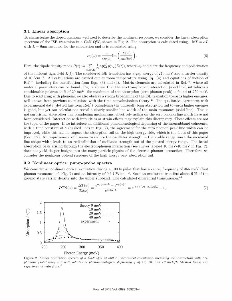
3.1 Linear absorptionTo characterize the doped quantum well used to describe the nonlinear response, we consider the linear absorptionspectrum of the ISB transition in a GaN QW, shown in Fig. 2. The absorption is calculated using −lnT = αLwith L = 6nm assumed for the calculation and α is calculated using:
α0(ω) =ω
cn(ω)Im
(P (ω)
ε0E(ω)
). (6)
Here, the dipole density reads P (t) :=∑
n,n′,k
1ω0
epn′nkpn
n′k(E(t)), where ω0 and e are the frequency and polarization
of the incident light field E(t). The considered ISB transition has a gap energy of 270 meV and a carrier densityof 1013cm−2. All calculations are carried out at room temperature using Eq. (4) and equations of motion ofRef.14 including the contribution from Eqs. (3) and (4). Matrix elements are calculated in Ref.23, where allmaterial parameters can be found. Fig. 2 shows, that the electron-phonon interaction (solid line) introduces aconsiderable polaron shift of 20 meV, the maximum of the absorption (zero phonon peak) is found at 250 meV.Due to scattering with phonons, we also observe a strong broadening of the ISB transition towards higher energies,well known from previous calculations with the time convolutionless theory.23 The qualitative agreement withexperimental data (dotted line from Ref.5) considering the unusually long absorption tail towards higher energiesis good, but yet our calculations reveal a clearly smaller line width of the main resonance (solid line). This isnot surprising, since other line broadening mechanisms, effectively acting on the zero phonon line width have notbeen considered. Interaction with impurities or strain effects may explain this discrepancy. These effects are notthe topic of the paper. If we introduce an additional phenomenological dephasing of the intersubband coherence,with a time constant of γ (dashed lines in Fig. 2), the agreement for the zero phonon peak line width can beimproved, while this has no impact the absorption tail on the high energy side, which is the focus of this paper(Sec. 3.2). An improvement of γ seems to reduce the oscillator strength in the visible range, since the increasedline shape width leads to an redistribution of oscillator strength out of the plotted energy range. The broadabsorption peak arising through the electron-phonon interaction (see curves labeled 10 meV-40 meV in Fig. 2),does not yield deeper insight into the many-particle physics of the electron-phonon interaction. Therefore, weconsider the nonlinear optical response of the high energy part absorption tail.
3.2 Nonlinear optics: pump-probe spectraWe consider a non-linear optical excitation during a 100 fs pulse that has a center frequency of 355 meV (firstphonon resonance, cf. Fig. 2) and an intensity of 9.6 GWcm −2. Such an excitation transfers about 6 % of theground state carrier density into the upper subband. The calculated differential transmission:24
DTS(ω) =∆T (ω)T0(ω)
=eαPP (ω)L − eα0(ω)L
eα0(ω)L= e[αPP (ω)−α0(ω)]L − 1, (7)
0
0.5
1
1.5
2
200 250 300 350 400
Abs
orpt
ion
-ln(
T)
Photon Energy (meV)
theory 0 meV10 meV20 meV40 meV
experiment
Figure 2. Linear absorption spectra of a GaN QW at 300 K, theoretical calculation including the interaction with LO-phonons (solid line) and with additional phenomenological dephasing γ of 10, 20, and 40 meV/h (dashed lines) andexperimental data from.5
Proc. of SPIE Vol. 6892 689209-4
is shown in Fig. 3 (solid lines) for different time delays τ between pump and probe pulse. Data (experimentaldetails can be found in Ref.5) are shown as dots. A detailed derivation of the formula for αpp is given in Ref.,25
only the ω-dependence is not neglected in this treatment, so that the ω dependent prefactors are kept (cf. thelinear case Eq. (6)). Especially for negative delay times (probe before pump, see Fig. 3 a), we obtain a dispersivesignature around the single particle transition energy, due to the off-resonant excitation (Stark effect).26 Theposition of the resonance has to be identified with the zero crossing at 250 meV. One phonon energy above thesingle phonon energy (355 meV) we find a resonant signature in the DTS spectra, which shows a very similarbehavior in theory and experiment and decays rapidly after the excitation.5 This signature is caused by thedynamical Stark effect during the overlapping pulses. Only a non-Markovian treatment of the EPI can revealthis effect, while a Markovian theory fails in second order Born approximation (not shown).
The theoretical results show deviations, in particular line shifts, from the experiment around the zero phononline at 250 meV. We attribute these deviation to similar processes discussed for the linear absorption, Sec. 3.1,like Coulomb effects or strain induced effects. In particular, electron localization effects in the plane of the wellmay resemble to a more level like response5 in comparison to the bulk response shown here. Our main point isto show that the phonon replica at 355 meV is clearly enhanced in nonlinear (Fig. 3) in comparison to the linearspectroscopy (Fig. 2).
One might wonder, why the energetic distance between the two resonant signatures is not exactly equal to thephonon energy like it was with the two level assumption in.5 We attribute the reason for this to the electronicdispersion inside the quantum well subband: With the resonant excitation at the first phonon side band, apart of the polaronic states connected to electron distribution in the subband are mostly resonantly excited,nevertheless these states have a less effective dipole moment than the main peak (cf. Fig 2). Additionally, theelectrons inside the subbands that cause the main linear absorption peak are non-resonantly excited, where theexcitation strength is determined by their dipole moment and the invidual detuning. Such effects cannot occurin a two level system system and are specific to the two subband system.
0
0.02
0.04
200 250 300 350
Dif
fere
ntia
l Tra
nsm
issi
on D
TS
(a)-50 fs
200 250 300 350
Photon Energy (meV)
(b)0 fs
200 250 300 350 400
(c)50 fs
theoryexperiment
Figure 3. DTS spectra at different delay times (a) -50 fs, (b) 0 fs, (c) 50 fs. The sample is nonlinearly excited with asecond 100 fs pulse at the first phonon replica around 355 meV.
4. RELAXATION DYNAMICS AT THE SILICON (001) 2×1 SURFACE
Electron relaxation phenomena at silicon surfaces are a topic of recent research.27, 28 A characteristic detail ofthe silicon (001) surface is the reconstruction incorporating a tilted dimer.7, 8 In the band structure, this featureresults in the formation of additional surface bands located partly inside the semiconductor bandgap.9 Thesesurface bands (Dup and Ddown)are related to the p-orbitals of the dimer atoms.8 While the Dup band is a valenceband, the Ddown band is not populated at zero temperature. In experimental studies,27, 28 it has been found thatthe phonon-induced relaxation inside the conduction bands is a complex process on multiple timescales. Theinterplay of interband scattering from the bulk to the Ddown band and intraband scattering inside the Ddown
bands are found to be the dominating processes. In this section, we use the Markovian dynamical equations (5) to
Proc. of SPIE Vol. 6892 689209-5
[eV
]
-10
-5
0
5
10
Γ X M X’ Γ
[eV
]
-10
-5
0
5
10
Γ X M X’ Γ
Figure 4. Electronic DFT-LDA band structures and atomic structures for supercells with 7 layers (lhs) and 40 layers (rhs).Besides the bulk-related bands (grey shaded regions), the Dup and Ddown bands are observable in the band gap.
calculate the population dynamics at the Silicon 2×1 surface, while the surface bandstructure and wave functionscalculated preliminarily by DFT.29
4.1 Linking density-functional theory and density-matrix theory
Phonon induced relaxation dynamics at the silicon (001) surface is investigated in terms of a two-step model.In a first step, the electronic structure of the surface structure is computed using DFT within the local-densityapproximation (LDA).30 The calculation is performed in the supercell-approach,9 with a reconstruction of 3layers at the surface, while at the other end of the structure, the chemical bonds are saturated by hydrogenatoms. The implementation of the DFT computer code uses plane-wave-basis set and pseudopotentials. In thesecond step, the population dynamics is calculated using the results of the first (DFT) step by DMT in theMarkovian limit.
DFT: In Fig. 4, the electronic band structures are shown for supercells of 7 layers and 40 layers. The atomicpositions and the size of the supercell are plotted by a ball-and-stick model for those two structures. The numberof bulk-bands is highly dependent on the number of layers in the calculation, and for a reasonable sampling of theband structure, obviously a fairly thick slab (� 20 layers) is needed to model the bulk effects of a single surface.Due to the description of the bandstructure within DFT-LDA, the semiconductor band-gap is underestimated byca. 0.52 eV with respect to the experimentally provided values.10, 30 As the electron dynamics is only investigatedfor the conduction bands by our approach and this shift of the band-gap energy is mostly independent of thek-location, this effect has no big influence on the conduction band structure and it is a good approximation touse the Kohn-Sham eigenvalues of the DFT-LDA calculation for the further discussion of the dynamics.
DMT: The electronic structure from the DFT calculations is now used to perform calculations on the electronpopulation dynamics of the conduction band states using Eq. (5). Using Kohn-Sham eigenvalues from the DFT-LDA calculation (step 1), the properties of the silicon surface enter into these equations of motion via the electronfield interaction pmk
nk (momentum matrix elements) and the electron-phonon coupling parameters:
gn′k′nk,iq = giq
∑
G,G′u∗
nk(G)un′k′(G′)δk+G,k′+G′+q. (8)
Here, umk′(G′) represent electronic Bloch waves in the k-space representation (Fourier transform of the realspace representation). Through the inhomogeneous delta condition in this equation (where the k vectors are notgenerally decoupled from the reciprocal lattice vectors G), a scattering over the Brillouin zone boundary can be
Proc. of SPIE Vol. 6892 689209-6
(r)
n’k’
(r)
unk
r u
3 d ∫
0.1
0.2
0.3
0.4
0.5
0.6
0.7
0.8
0.9
1
kΓ X M ’X Γ
k’
Γ
X
M
’X
Γdown D↔ down
7 layer - D down D↔ down7 layer - D
(r)
n’k’
(r)
unk
r u
3 d ∫
0
0.1
0.2
0.3
0.4
0.5
0.6
0.7
0.8
0.9
1
kΓ X M ’X Γ
k’
Γ
X
M
’X
Γ bulk↔7 layer - bulk bulk↔7 layer - bulk
(r)
n’k’
(r)
unk
r u
3 d ∫
0
0.1
0.2
0.3
0.4
0.5
0.6
0.7
kΓ X M ’X Γ
k’
Γ
X
M
’X
Γ bulk↔ down
7 layer - D bulk↔ down7 layer - D
(r)
n’k’
(r)
unk
r u
3 d ∫
0
0.05
0.1
0.15
0.2
0.25
0.3
kΓ X M ’X Γ
k’
Γ
X
M
’X
Γ bulk (umklapp)↔ down
7 layer - D bulk (umklapp)↔ down7 layer - D
Figure 5. Square modulus of the electron matrix elements for different transitions. Top row: intraband transitions, insideDdown band (lhs) and inside lowest bulk conduction band (rhs), bottom row: interband transition from Ddown band tofirst bulk band (lhs) and corresponding umklapp process via zone boundary. The transition are shown for a transitionfrom an an initial state to a final state on the symmetry line.
described. For small k and q however, the general delta condition falls back to the commonly used momentumconservation condition k = k′ + q.
While the phonon-mode dependent coupling parameter giq is approximated by typical values from bulksilicon,31 the part In′k′
nk =∑
G,G′ u∗nk(G)un′k′(G′) depends on the electronic wave functions of the underlying
structure. Here, the Kohn-Sham wave functions are used to calculate the electron-state dependent transitionamplitudes for all involved bands. In Fig. 5, the modulus of the transition integrals In′k′
nk of the electronic wavefunctions is depicted. For the intraband transitions (top row of Fig. 5), the modulus approaches a value of 1 on thediagonal (q = 0, initial and final states are the identical). Furthermore, for intraband scattering, the modulusremains unchanged with respect to the exchange of inital and final states, and in place of the correspondingsymmetrical representation, an umklapp process is plotted in the upper left half of the top row pictures in Fig. 5.It is obvious that the scattering via umklapp process is only of minor importance for this intraband scattering(one order of magnitude less than via direct scattering). For the interband processes (bottom row of Fig. 5),scattering is limited to some specific points within the Brillouin zone (here, scattering on the diagonal is alwaysvanishing, as initial and final states are orthogonal for different bands at the same k-point). Furthermore, theumklapp-scattering (rhs of the bottom row of Fig. 5) now differs only by a factor of 3 from the direct processes.As a consequence, we cannot generally neglect the scattering over the Brillouin zone boundary. We note thatthese considerations are focused on one part of the electron-phonon scattering processes (In′k′
nk ), while the phononmode dependent form factor giq and scattering in the equations of motion Eq. (5) is highly dependent on thewave number q as the scattering matrices (4) contain the energy conservation for the scattering processes. Inthe numerical simulation of Eq. (5), all these effects are taken into account.
The discussion of the involved electron-phonon interaction induced relaxation dynamics is investigated usingEq. (5). The initial population in this approach is provided by simulating the linear absorption of a finite-
Proc. of SPIE Vol. 6892 689209-7
energy [eV]0 0.5 1 1.5 2 2.5 3 3.5 4 4.5 5
[a.
u.]
α
0
0.002
0.004
0.006
0.008
0.01
0.012
0.014
0.016
0.018
bulk
7 layers10 layers15 layers22 layers
30 layers40 layers
energy [eV]0.5 0.6 0.7 0.8 0.9 1 1.1 1.2 1.3
[a.
u.]
α
0
0.02
0.04
0.06
0.08
0.1
0.12
0.14
-310×
bulk
7 layers10 layers15 layers22 layers
30 layers40 layers
Figure 6. Linear absorption spectra for the Si 2×1 (001) surface for different supercell structures and for the bulk. Onthe rhs, a cutout of the full spectrum at the lhs is shown.
length optical pulse without considering the interference of the optically induced electron preparation with therelaxation dynamics.
4.2 Linear spectra
The linear spectrum of the silicon 2×1 surface can be calculated according to Eq. (6). In Fig. 6, linear spectraare shown for a variety of supercells with increasing slab thickness. Within these plots, only the direct opticaltransitions (via the matrix elements pn′k
nk , Eq. (1)) are considered, while indirect optical scattering and relaxationprocesses are neglected. On the lhs of Fig. 6, the spectrum is shown in the range from 0 eV to 4 eV. Whilesignificant differences are observable for the different surface supercells the onset of the bulk spectrum is onlyvisible above 2.7 eV (due to the indirect bandgap of silicon), while there are pronounced contributions to thesurface spectra at lower energies (2.0 - 2.5 eV). These additional transitions in the spectrum are related to theDdown surface band in the band structure (Fig. 4). In the cut of the spectrum (rhs of Fig. 6) for the range of0.5-1.3 eV, all visible peaks are related to transitions from the valence bands to the Ddown band. Due to thescissors shift (cf. Sec. 4.1), the optical pulse used for the simulation of the relaxation dynamics corresponds to apulse of 1.07 eV in the DFT-LDA bandstructure.
The initial population for the relaxation dynamics discussed in the next section is consequently induced bysome of the peaks in Fig. 6 (rhs). Furthermore, the position of some the peaks differs in this figure between theslabs (the height of the peaks is decreased with increasing layer number due to a volume-surface effect). As aconsequence, for the simulation of optical excitation in the very narrow energy range of 0.5-1.3 eV, a big layernumber is obviously needed.
4.3 Relaxation dynamics
The evolution of the population of the conduction band states is shown in Fig. 7 for two supercells of 7 (lhs)and 40 layers (rhs). At top level, the corresponding conduction band structure is depicted, where the zero ofthe energy axis corresponds to the minimum of the Ddown band (the leftmost bands in the two bandstructurepictures in Fig. 7). The inital occupation10
f initialnk =
1h2
∑
m
∣∣∣∣pmnkA
(εmk − εnkh
)∣∣∣∣2
(9)
with the Fourier-transform optical vector potential A(ω) is calculated for an optical pulse of 1.69 eV (correspond-ing to 1.07 eV in the LDA-bandstructure) and 100 fs duration. Only a few bands are located in the relevantoptical excitation energy range which can be populated: For the 7-layer slab, the entire relaxation process ex-tends on 2 bands (the Ddown and one bulk band), for the 40-layer slab, about 10 bands are in the ”active region”.
Figure 7. Relaxation dynamics after initial excitation with optical initial conditions for a slab of 7 layers and 40 layers.
In both calculations, the major part of the initial population is located within a few states at about 0.46 eV,but the energetical localization is much narrower in the 40 layer calculation. By projection to real space (Fig.8), it can be seen that this initial population is almost completly inside the surface band, while the bulk band(s)are not strongly populated by the optical excitation.
It is clearly visible in Fig. 7 (bottom) that the relaxation processes out of a non-equilibrium initial situation toa quasi-equilibrium final state happens on multiple timescales and includes the whole energy scale of the energydispersion. The shape of the initial distribution is dispersed fast (30 fs), and after 50 fs, a significant populationof the conduction band minimum is found. While this fast timescales do not differ for the two supercells, largerdifferences can be found after 100 fs: for the 7-layer supercell, a strong population forms at the energetic position
Proc. of SPIE Vol. 6892 689209-9
0 ps
2 ps
190 ps
Figure 8. Projection of the conduction band population into the real space for timesteps of 0, 2 and 190 ps. While theinitial population is strongly localized at surface, the population partly shifts to the bulk at 2 ps, and finally returns intoa surface state (minimum of Ddown-band).
of the (single) bulk band minimum (0.24 eV), reaching its maximum at 500 fs and is almost gone after 2 ps. Atthis timestep, the rest of the population already resembles a fermi distribution at the conduction band minimum.For the 40-layer supercell, the lowest bulk band minmum is at 0.08 eV, and a local population maximum formsat 0.08-0.1 eV. Both the formation time of this population accumulation and the decay time are much longerthan for the 7-layer case: the maximum is reached at about 2 ps, and some minor peaks are still present at 200 psrelaxation time. As an obvious conclusion, we can see that the relaxation highly depends on the slab thicknessleading to a electronic band structure in the involved energetic region relevant for the relaxation processes (andthus the representation of the supercell with only a few layers is insufficient to calculate the relaxation process).
By comparing this specific relaxation behaviour (Fig. 7) in the real-space representation (Fig. 8), it can beseen that the slower relaxation processes (2 ps) are obviously related to a population of the bulk bands (afterthe initial preparation at the surface) and a subsequent backscattering to the surface state (the conduction bandminimum of the surface band structure is in the Ddown-band). A qualitative explanation of the involved processesis that the intra-surface-scattering is much stronger than the bulk-scattering due to the difference in the strengthof the related matrix elements (cf. Fig. 5). A more quantitative discussion of the relaxation will be done in thenext paragraph. In any case, the relaxation via the bulk states is an alternative (but slow) relaxation channelto the direct intraband relaxation inside the surface band.
The dependence of the relaxation times on the supercell thickness can be investigated by an examination ofthe population of the conduction band minimum (which is also the minimum of the Ddown band). In Fig. 9,the time-dependent population of the state representing the minimum is drawn on a logarithmic timescale. Twotimescales can be clearly identified (lhs of Fig. 9): At the beginning of the relaxation (t <1 ps), the state ispopulated with on a ps-timescale. At the end of relaxation (middle of Fig. 9), a much slower timescale highlysensitive to the supercell size applies. The dashed lines refer to the exponential fit functions to extract numericalvalues for the timescales. Those extracted timescales are visualized in Fig. 9 (rhs) for different supercells ona logarithmic scale: While the short-term time-scale remains close to the 1 ps relaxation time for all differentsupercells, the long-term timescale varies from 2.5 ps (7-layer slab) to 60.0 ps (40-layer slab), where a thickerslab generally leads to a slower relaxation. This can by explained by the interplay of the scattering via electron-optical and -acoustical phonons: The intraband scattering inside the surface band is always dominated by opticalphonons due to the fairly strong bending of the band in the X − M -direction. The same explanation appliesfor the scattering from the surface-band to bulk states. The character of the scattering from bulk to surface fora specific supercell, however, depends strongly on the actual position of the bulk bands in the band structure(Fig. 4): while for 7 bands, an energetical gap of 0.2 eV between the lowest bulk band and the minimum of theDdown-band is observable, this gap is only about 0.01 eV for the 40 layer slab. As a consequence, for 7 layers,
Proc. of SPIE Vol. 6892 689209-10
time [ps]-110 1 10 210 310
min
f
0
0.2
0.4
0.6
90 K 7 layers22 layers30 layers40 layers
time [ps]10 210 310
min
f
0.58
0.6
0.62
0.64
0.66
90 K 7 layers22 layers30 layers40 layers
No. of layers7 10 15 22 30 40
rela
xatio
n tim
e [p
s]
1
10
No. of layers7 10 15 22 30 40
rela
xatio
n tim
e [p
s]
1
10
Figure 9. Relaxation timescales of the Si 2×1 surface for different supercells. On the lhs, the population of the conductionband minimum (Ddown-band) is shown on a logarithmic timescale. In the middle column, a cutout of this populationdynamics is drawn for times gt. than 10 ps. On the rhs, the relaxation timescales extracted from the lhs. data is shownfor the different supercells.
also bulk-surface scattering is dominated by optical scattering, whereas for 40 layers only acoustical phononsallow to override the small energy gap. As the optical phonons are both coupled by a much stronger deformationpotential (5× stronger than for acoustical phonons) to the electrons and the energy transfer per scattering eventis bigger for optical phonons, the typical relaxation times for an optical-phonon mediated scattering are muchfaster than for acoustical scattering.
5. CONCLUSION
We have reviewed a theory for the description phonon-induced relaxation phenomena in two dimensional sys-tems. By applying this theory to nonlinear optical properties of phonon assisted intersubband transitions inGaN including the non-Markovian nature of the electron-phonon interaction, our numerical calculations agreequalitatively with recent experimental work5 and shows a satellite peak due to LO electron-phonon interaction,which is clearly visible only in nonlinear pump probe spectra. Our conclusion is that pump probe spectroscopyis appropriate to uncover non-Markovian polaron effects, that are not visible in linear spectra. The investiga-tion of phonon induced relaxation at the silicon 2×1 (001) surface reveals a complex relaxation process on twotimescales involving surface-surface and bulk-surface scattering. The timescales are in agreement to experimentalfindings recently published28 and the different magnitude can be related to optical phonon scattering inside theDdown-surface band for the fast timescale and acoustical phonon scattering for the slower processes from thebulk to the surface band.
The authors acknowledge financial support by the Deutsche Forschungsgemeinschaft through KN 427 4-1,KN 427 3-1, SPP 1093, Sfb 787 and the CoE UniCat.
REFERENCES1. M. Lindberg and S. W. Koch, “Effective bloch equations for semiconductors,” Phys. Rev. B 38, pp. 3342–
3350, Aug 1988.2. T. Kuhn, Theory of Transport Properties of Semiconductor Nanostructures, ch. 6, p. 173. Chapman & Hall,
London, 1998. edited by E. Scholl.3. F. Rossi and T. Kuhn, “Theory of ultrafast phenomena in photoexcited semiconductors,” Rev. Mod.
Phys. 74(3), pp. 895–950, 2002.4. J. Schilp, J. Kuhn, and G. Mahler, “Electron-phonon quantum kinetics in pulse-excited semiconductors:
Memory and renormalization effects,” Phys. Rev. B 50(8), p. 5435, 1994.5. Z. Wang, K. Reimann, M. Woerner, T. Elsaesser, D. Hofstetter, J. Hwang, W. J. Schaff, and L. F. East-
man, “Optical phonon sidebands of electronic intersubband absorption in strongly polar semiconductorheterostructures,” Phys. Rev. Lett. 94, p. 037403, 2005.
Proc. of SPIE Vol. 6892 689209-11
6. Z. Wang, K. Reimann, M. Woerner, T. Elsaesser, D. Hofstetter, E. Baumann, F. R. Giorgetta, H. Wu,W. J. Schaff, and L. F. Eastman, “Ultrafast hole burning in intersubband absorption lines of gan/alnsuperlattices,” Appl. Phys. Lett 89, p. 151103, August 2006.
7. J. Fritsch and P. Pavone, “Ab initio calculation of the structure, electronic states, and the phonon dispersionof the Si(100) surface,” Surf. Science 344, p. 159, 1995.
8. A. Ramstad, G. Brocks, and P. J. Kelly, “Theoretical study of the Si(100) surface reconstruction,” Phys.Rev. B 51, p. 14504, 1995.
9. N. Buecking, P. Kratzer, M. Scheffler, and A. Knorr, “Theory of optical excitation and relaxation phenomenaat semiconductor surfaces: linking density functional and density matrix theory,” Appl. Phys. A 88, p. 505,2007.
10. N. Buecking, P. Kratzer, M. Scheffler, and A. Knorr, “Linking density-functional and density-matrix theory:picosecond electron relaxation at the Si(100) surface,” submitted to Phys. Rev. Lett. , 2007.
11. A. Zeiser, N. Bucking, J. Gotte, J. Forstner, P. Hahn, W. G. Schmidt, and A. Knorr, “Dynamics ofthe phonon-induced electron transfer between semiconductor bulk and surface states,” Phys. Status Solidi(b) 241, p. R60, 2004.
12. A. Zeiser, N. Bucking, J. Forstner, and A. Knorr, “Microscopic theory of electron dynamics and time-resolvedtwo-color two-photon photoemission at semiconductor surfaces,” Phys. Rev. B 71, p. 245309, 2005.
13. J. Hader, S. W. Koch, J. V. Moloney, and E. P. O’Reilly, “Influence of the valence-band offset on gain andabsorption in ganas/gaas quantum well lasers,” Appl. Phys. Lett. 76(25), pp. 3685–3687, 2000.
14. S. Butscher, J. Forstner, I. Waldmuller, and A. Knorr, “Polaron signatures in the line shape of semiconductorintersubband transitions: quantum kinetics of the electron-phonon interaction,” Phys. Status Solidi (b) 11,pp. R49–R51, 2004.
15. S. Butscher, J. Forstner, I. Waldmuller, and A. Knorr, “Ultrafast electron-phonon interaction of inter-subband transitions: Quantum kinetics from adiabatic following to rabi-oscillations,” Phys. Rev. B 72,p. 045314, 2005.
16. S. Butscher, Many-Particle Effects in Two Dimensional Nanostructures: Semiconductor In-tersubband Transitions and Graphene. PhD thesis, Technische Universitat Berlin,http://nbn-resolving.de/urn:nbn:de:kobv:83-opus-16022, 2007.
17. I. Waldmuller, J. Forstner, S.-C. Lee, A. Knorr, M. Woerner, K. Reimann, R. A. Kaindl, T. Elsaesser,R. Hey, and K. H. Ploog, “Optical dephasing of coherent intersubband transitions in a quasi-two-dimensionalelectron gas,” Phys. Rev. B 69(20), p. 205307, 2004.
18. J. Li and C. Z. Ning, “Induced transparency by intersubband plasmon coupling in a quantum well,” Phys.Rev. Lett. 93(8), p. 087402, 2004.
19. B. Krummheuer, V. M. Axt, and T. Kuhn, “Theory of pure dephasing and the resulting absorption lineshape in semiconductor quantum dots,” Phys. Rev. B 65, p. 195313, May 2002.
20. J. Forstner, K. J. Ahn, J. Danckwerts, M. Schaarschmidt, I. Waldmuller, C. Weber, and A. Knorr, “Lightpropagation- and many-particle-induced non-Lorentzian lineshapes in semiconductor nanooptics,” Phys.Status Solidi (b) 234(1), pp. 155–165, 2002.
21. R. Zimmermann and E. Runge, “Dephasing in quantum dots via electron-phonon interaction,” in Proc. 26thICPS Edinburgh, A. R. Long and J. H. Davies, eds., IOP Conf. Series 171, IOP Publishing Bristol (UK),2002. paper M 3.1.
22. V. Meden, J. Fricke, C. Wohler, and K. Schonhammer, “Hot electron relaxation in one-dimensional models:exact polaron dynamics versus relaxation in the presence of a fermi sea,” Z. Phys. B , 1995.
23. S. Butscher and A. Knorr, “Theory of strong electron-phonon coupling for ultrafast intersubband excita-tions,” Phys. Status Solidi (b) 243(10), pp. 2423–2427, 2006.
24. H. Haug and S. Koch, Quantum Theory of the Optical and Electronic Properties of Semiconductors, WorldScientific, Singapore, 2004.
25. M. Richter, T. Renger, and A. Knorr, “A bloch equation approach to intensity dependent optical spectraof light harvesting complex ii,” Photosynthesis Research , 2007. doi:10.1007/s11120-007-9256-z.
26. S. W. Koch, N. Peyghambarian, and M. Lindberg, “Transient and steady-state optical non-linearities insemiconductors,” J. Phys. C 21, pp. 5229–5249, 1988.
Proc. of SPIE Vol. 6892 689209-12
27. S. Tanaka and K. Tanimura, “Time-resolved two-photon photoelectron spectroscopy of the Si(001)-(2 × 1)surface,” Surf. Science 529, p. 251, 2003.
28. M. Weinelt, M. Kutschera, T. Fauster, and M. Rohlfing, “Dynamics of exciton formation at the Si(100)c(4 × 2) surface,” Phys. Rev. Lett. 92, p. 126801, 2004.
29. P. Hohenberg and W. Kohn, “Inhomogeneous electron gas,” Phys. Rev. 136, p. B 864, 1964.30. P. Rinke, A. Qteish, J. Neugebauer, C. Freysoldt, and M. Scheffler, “Combining GW calculations with
exact-exchange density-functional theory: an analysis of valence-band photoemission for compound semi-conductors,” New Journal of Physics 7, p. 126, 2005.