There is an increasing demand for new devices thatcan be used in optical communications networks.1–3
Such devices will have high operating speeds andbroad working spectral domains and will be subject toboth optical and electrical control. Among the de-vices that are key components of an optical commu-nications network are included modulators,photodetectors, and devices used for data storage aswell as those that exhibit optical bistability.
There have been many successful attempts to con-ceive and fabricate such devices. The interestedreader can find in Ref. 4 an overview of the subject.However, a device that incorporates many of thefunctions mentioned above, which will be easier tomanufacture than other devices and will permit theuse of a large variety of materials, will be of greatinterest for use in optoelectronics and optical commu-nications. Moreover, if such a device allows the tai-loring of its working spectral domain in the bandspanning the visible to the mid infrared, with a band-width of approximately 0.1–0.2 eV �for a given de-
vice�, it can be considered one of the most importantcandidates for use in future optical networks.
Such a device is the tunnel diode described previ-ously in Ref. 5. The theory of the basic optoelec-tronic behavior of a tunnel diode is presented here.To my knowledge, the tunnel diode has not yet beenused as an optoelectronic device. I show that it canact as a high-speed ��40-GHz�, high-performanceelectro-optic modulator driven by voltages of �3 V.Moreover, the tunnel diode exhibits optical bistabilityand self-induced transparency. One controls its out-put and working parameters �such as switch-on andswitch-off of incident powers in the bistable domain�by manipulating the power of the input light, theapplied voltage, and the number of times that thelight beam passes through the device. The workingspectral domain is very large, of the order of 0.1–0.2eV, for a given device.
We shall consider only the basic �intrinsic� opto-electronic behavior and the fact that the tunnel diodeworks in the open-circuit regime. We do not con-sider any electrical circuit �containing loads, capaci-tances, inductances� to which the tunnel diode isconnected, except a high-impedance voltage source.We do not consider the case when the tunnel diode isplaced inside a Fabry–Perot resonator. The twolast-named cases deserve separate study and are notsubjects of this paper.
The paper is structured as follows: Section 2 isdevoted to a brief presentation of the interaction be-tween light and degenerate semiconductors. Bothabsorption and propagation are considered. Section3 is devoted to presentation of the working regimes of
The author �[email protected]� is with the National Institutefor Research and Development in Microtechnology, Str. Erou IancuNicolae 32B, 72996, Bucharest, Romania and can be reached atAleea Fuiorului Number 6 block Y3A, Section 1 et.6 ap. 27, Sector3, Bucharest, Romania.
the tunnel diode when it is used as an optoelectronicdevice. There are three main regimes: electro-optic modulation, optical bistability, and self-inducedtransparency. In Section 4 we discuss these threekinds of behavior, make numerical estimations ofsome of the device optoelectronic parameters, andcompare this tunnel diode with other existingsemiconductor-based optoelectronic devices. Someconclusions are given in Section 5.
2. Absorption of Light in a Tunnel Diode
Before considering the way in which light is absorbedin a tunnel diode, we consider how absorption of lightoccurs in degenerate semiconductors.
One obtains a degenerate semiconductor by heavilydoping the semiconducting substrate with an appro-priate dopant. In a degenerate semiconductor theFermi level lies within the energy band that com-prises the majority charge carriers �conduction bandfor n type, valence band for p type�. The situation isdepicted in Fig. 1. All the levels situated below theFermi level are occupied, whereas the levels situatedabove are free.6,7
In Fig. 1, Eg is the energy bandgap of the semicon-ductor and E1 and E2 are the energy differences be-tween the Fermi level and the bottom of theconduction band and between the top of the valenceband and the Fermi level, respectively. It must betaken into account that energy bandgap Eg does notrepresent the true energy bandgap Eg0 of an undopedsemiconductor. This is so because the impurity en-ergy level in a heavily doped semiconductor becomesan energy band. This impurity energy band over-laps the corresponding energy band of the semicon-ductor �the conduction band for n-type and thevalence band for p-type semiconductors�, decreasingthe initial bandgap of the host material. The differ-ence Eg0 � Eg can attain values as high as 0.3 eV.
All the following properties and conditions with
respect to the absorption of light in heavily dopedsemiconductors and in tunnel diodes are valid, withthe caution just mentioned concerning the value ofthe energy bandgap in a degenerate semiconductor.
Let now consider Fig. 1�a�. Only the process la-beled 3 gives rise to photogenerated charge carriers.This process takes place for a photon with an energyEg � E1 � h�.
Figure 1�b� is similar. Again, process 3 is the onlyone that gives rise to photogenerated charge carriers.The photon energy satisfies the relation Eg � E2 �h�. Details of optical absorption in heavily dopedsemiconductors, as well as of the effect of a blueshiftof fundamental absorption in such materials �theMoss–Burnstein effect� can be found in Ref. 8.
Now we shall consider a tunnel diode. Its energy-band diagram in the equilibrium state �i.e., at noexternal electrical polarization�, is presented in Fig.2. The light is traveling along the O–X axis.
All the notation is as above. Vb denotes the volt-age barrier of the p–n junction. Consider an inci-dent photon that has an energy h� � Eg �in fact, theenergy is slightly above Eg�. This photon will beabsorbed only in that region where an occupied stateexists in the valence band and an empty state existsin the conduction band, where these two states areseparated by an energy equal to h�. Thus, for thiscase, the absorption will occur between points B andC in Fig. 2.
Consider now a photon that has an energy h� thatsatisfies the relation Eg � h� � Eg � min �E1, E2�.In this case, no absorption will occur in the p or the nregion. In the junction the absorption will occuronly when Eg � E1 � h�, or Eg � E2 � h�, respec-tively. This means that the absorption region is sit-uated between points G and F of Fig. 2 and is broaderthan in the previous case. The positions of thesepoints are determined only by the photon energy.However, point G will always belong to the A–B in-
Fig. 1. Schematic representation of the energy levels and opticaltransitions in degenerate semiconductors for an n-type �a� and ap-type �b� semiconductor. Processes numbered with 1–3 refer toelectron interband transitions that are due to photon absorption.
Fig. 2. Schematic representation of the energy band structure ofa tunnel diode with no external electric polarization. The arrowindicates the direction of propagation of light.
terval, whereas point F will always belong to the C–Dinterval.
Consider now a photon with an energy that satis-fies the relation Eg � min�E1, E2� � h� � Eg �max�E1, E2�. In this case the photon will be stronglyabsorbed in that region for which Eg � min�E1, E2� �h�. Absorption will take place also in the p–n junc-tion but will be bounded by the condition that E �h�, where E is the energy necessary for an electron tobe taken from the valence band and transferred to theconduction band. The last case corresponds to thatof a photon with Eg � max �E1, E2� � h�. In thiscase the absorption takes place throughout the wholediode structure. It must be noted that only the ra-diation absorbed in the p–n junction gives rise to thephotovoltaic effect.
As one can therefore conclude, only the case Eg �h� � Eg � min �E1, E2� could be of interest for pho-tonic applications, because then the flux of incidentlight is absorbed only in the p–n junction; the rest ofthe diode is practically transparent �see the discus-sion below� to incoming light.
Thus, by modulating the length of the space-chargeregion of the diode, we can modulate the length ofabsorption of light within the device. This modula-tion can be easily achieved by application of an ex-ternal voltage to the diode. This case corresponds tothat of an electro-optic modulator. But the absorbedlight gives rise to a voltage, too, as a result of thephotovoltaic effect that occurs in the p–n junction.This is the case when the incident beam self-modulates its transmission through the device.These two regimes are discussed in Section 3 below.
Before discussing the working regimes mentionedabove, we discuss two other mechanisms that con-tribute decisively to the propagation of light in a tun-nel diode. The first is absorption of light by freecharge carriers. The second is the propagation oflight waves inside the free-charge-carrier plasma.
The coefficient f of absorption by the free chargecarriers is given by9,10
f ��
c ���4��2 � �p2� � �p
4�2 1�2
�3 ��2 � �p
2
�2 � , (1)
where �p is the plasma frequency and � is the colli-sion frequency of the free charge carriers. c is thespeed of light and � is the frequency of the input lightbeam. Equation �1� is valid when the input lightbeam’s frequency is higher than the collisional fre-quency of the charge carriers. Plasma frequency �pis9,10
�p � �q2n�εm�1�2, (2)
where q is the unit electric charge, n is the concen-tration of free charge carriers, and m denotes thefree-charge-carrier effective mass, while ε denotesthe electric permittivity.
As can be seen, both f and �p increase with theconcentration of free charge carriers �and hence ofdopant�. As was mentioned in Refs. 9 and 10, an
electromagnetic wave can propagate through aplasma only if its frequency is higher than plasmafrequency �p.
Because the input light beam must reach thespace-charge region of the p–n junction, its frequencymust be higher than the plasma frequencies of boththe p and the n regions.
Thus we have the following set of conditions:
�� � ��p, (3a)
Eg � �� � Eg � min�E1, E2�. (3b)
From these two relations it is obvious that the fol-lowing condition must be obeyed:
��p � Eg, (4)
or, for each region of the device:
h2� � q2n
εmn�1�2
� Eg,
h2� � q2p
εmp�1�2
� Eg, (5)
where the subscripts n and p refer to electrons andholes, respectively.
These conditions establish the relation that mustexist among the bandgap value, the dopant concen-trations, and the effective masses of free charge car-riers in order that the incident light beam be able toreach the space-charge region. n and p depend onthe density of states in the respective bands as well ason the value of min�E1, E2� that must be obtained�and that fixes the working spectral domain of thetunnel diode as an optoelectronic device�.
If at least one of conditions �5� is not fulfilled, thelight cannot propagate inside the tunnel diode andthe device cannot act as an optoelectronic element.Even if at least one of conditions �5� is satisfied, theproblem that still remains is the absorption of lightby the free charge carriers that exist in the tunneldiode. As can be observed from Eq. �1�, the absorp-tion coefficient depends on the frequency of the inputlight as well as on the plasma frequency.
One way to reduce this unwanted absorption is byuse of a very thin semiconducting membrane �with athickness of 1–2 �m� inside which the tunnel diode issituated. However, this unwanted absorption alsodetermines the number of times that the light passesinside the device. Therefore it is desirable to workwith semiconductors that have wide bandgaps and alow charge-carrier mobility or whose degeneracy be-gins at a low critical concentration of dopant.
3. Working Regimes of the Tunnel Diode as anOptoelectronic Device
A. Electro-Optic Modulator
In electro-optic modulator regime, an external volt-age is applied to the diode. The voltage produces a
variation in the thickness of the space-charge regionof the p–n junction as described by7
d � �2εq
Na � Nd
Na Nd�Vb � V��1�2
. (6)
Here ε is the electric permittivity of the semicon-ductor, q � 1.6 � 10�19 C is the elementary charge,Na and Nd are the acceptor and donor concentrations,respectively, and V is the applied voltage.
As we mentioned in Section 2, the wavelength do-main that proves to be useful for optoelectronic ap-plications is that for which Eg � �� � Eg � min�E1,E2�. Let E be the electric field in the junction. Thethickness deff of the absorbing region �the length ofthe B–C region in Fig. 2� is
deff � d �E1 � E2
qE
�qVb � qV
qE�
E1 � E2
qE
�Eg � qV
qE, (7)
where we have used the relations
d �Vb � V
E,
qVb � Eg � E1 � E2. (8)
deff from Eq. �7� corresponds to the absorptionthickness for a photon that has �� � Eg �in fact, �� isslightly above Eg�.
The expression for field E is
E � � q2ε
Na Nd
Na � Nd�Vb � V��1�2
. (9)
Thus the expression for deff is
deff �1q �2ε
qNa � Nd
Na Nd�1�2 Eg � qV
�Vb � V�1�2 . (10)
It can be observed from Eq. �10� that a change inthe voltage applied to the tunnel diode modifies thick-ness deff of the region in which absorption of lightoccurs.
Transmittance T of the tunnel diode, for the radi-ation in the spectral domain considered above, is
T � exp��deffN�, (11)
where is the intrinsic absorption coefficient and Nrepresents the number of times the light crosses thep–n junction. For the usual case when the lightpasses only once through the junction, N � 1. But ifthe tunnel diode is placed between two mirrors, asdepicted in Fig. 3, the number of times that the lightpasses through the junction is N � 1.
Taking into account Eqs. �10� and �11�, we obtainfor the transmittance the expression
T � exp��N1q �2ε
qNa � Nd
Na Nd�1�2 Eg � qV
�Vb � V�1�2� . (12)
The plot T � f �V� is depicted in Fig. 4 for severalvalues of N �indicated on the plots� for the followingset of values: � 106 m�1, Na � 1020 cm�3, Nd �1020 cm�3, ε � 12ε0, Eg � 1.12 eV �for silicon�, Vb �1.27 V, and h� � Eg � 1.12 eV. ε0 � 8.8 � 10�12
F�m is the vacuum permittivity.As can be seen from Fig. 4, the applied voltage
modulates the optical transmittance of the tunneldiode. In this case the tunnel diode works as anelectroabsorption modulator. The electroabsorptionmodulator can work in two ways: �a� modulation ofthe value of deff, which happens for photon energythat corresponds to the condition Eg � h� � Eg �min�E1, E2� and �b� modulation of the absorption co-efficient by means of the Franz–Keldysh effect, which
Fig. 3. Schematic representation of the way in which light travelsin a tunnel diode placed between two mirrors �not a Fabry–Perotresonator�.
Fig. 4. Optical transmittance versus applied voltage for a tunneldiode used in the electro-optic modulator regime for several valuesof N.
happens for photon energy that fulfills the conditionh� � Eg. Compared with the self-electro-optic de-vice4,11 �SEED� that is based only on the Franz–Keldysh effect, the tunnel diode is more versatile,admitting two working possibilities and two spectraldomains for achieving modulation. Moreover, theallowed bandwidth of light for modulation is larger inthe tunnel diode �� min�E1, E2� than in a SEED.E1 and E2 are determined by the doping concentra-tions and by the effective masses of the free chargecarriers, respectively. Thus the tunnel diode allowsthe working spectral domain to be tailored by choiceof the appropriate doping. Such is not the case for aSEED.
From Fig. 4 it can be concluded that with a voltagesweep of approximately 3 V �from �2 to 1 V� thetransmittance varies from 8% to �100%.
Because the tunnel diode can be driven by voltagesthat can have frequencies of approximately 40 GHz,the maximum modulation frequency of the incidentoptical beam is of the order of 40 GHz.
Another factor that limits the maximum workingfrequency of the modulation is the distance betweenthe two mirrors in Fig. 3 as well as the number oftimes that the light passes through the junction. Ifthe distance between the mirrors is of the order of 100�m and the light passes 100 times through the junc-tion, then the maximum working frequency is �10GHz. One can increase this frequency by decreasingthe distance between the mirrors, decreasing thenumber of times that the light passes through thejunction, or both.
A problem must be mentioned for this kind of mod-ulator: When the intensity of the incident light ishigh, the incident beam generates photovoltageacross the junction. This means that the beam isable to self-modulate the transmitted intensity. Theproblem can be overcome by use of low-power inci-dent beams, as is done for optical communications.The problem of self-modulation is discussed in Sub-section 3.B below.
It is worthwhile to mention that, for operation inthe electro-optic modulator regime, the modulationfrequency must be higher that the maximum resis-tive cutoff frequency7 of the tunnel diode. In thiscase the tunnel diode has only a positive value for theimpedance. The maximum resistive cutoff fre-quency depends on the tunnel diode’s serial resis-tance, on its negative resistance value, on itsinductance �including terminals�, and on its junctioncapacitance when it is biased at the valley voltage.7
Another factor that must be taken into account isphase modulation of the traveling light beam. Thismodulation is due to the difference in the refractiveindices of the doped regions and of the space-chargelayer. Modulating the thickness of the space-chargelayer thus gives rise to a phase modulation. Butwhen one takes into account that the change in thespace-charge layer’s thickness is of the order of 10 nm�that is, almost a hundredth part of the radiationwavelength�, it results that the effect of phase mod-
ulation is not so important as that of intensity mod-ulation.
B. Self-Electro-Optic Modulator
In the self-electro-optic modulator regime, the light ismodulated by the photovoltage generated by the lightpassing through the junction. This situation is sim-ilar to that of the electro-optic modulator presented inSubsection 3.A; the only difference is that here thevoltage is generated by the incident light itself and itis not applied from an external source.
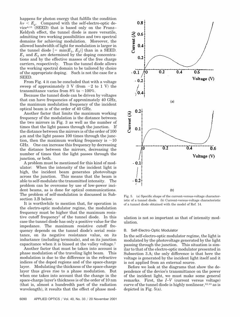
Before we look at the diagrams that show the de-pendence of the device’s transmittance on the powerof the incident light, we must make some generalremarks. First, the I–V �current versus voltage�curve of the tunnel diode is highly nonlinear,12,13 as isdepicted in Fig. 5�a�.
Fig. 5. �a� Specific shape of the current-versus-voltage character-istic of a tunnel diode. �b� Current-versus-voltage characteristicof a tunnel diode obtained with the model of Ref. 14.
Second, because the transmittance depends on theintensity of the incident light, one may expect a non-linear relationship between the intensities of outputand input light. Taking these two arguments intoaccount, we may expect the tunnel diode to be ahighly nonlinear optoelectronic device when it is usedas a self-modulator. Moreover, taking into accountthe shape of the tunnel diode’s I–V characteristics, wemay expect the device to exhibit optical bistability.
To compute the transmittance-versus-incident-power characteristics, we must know the analyticalexpression for the I–V characteristics. As presentedin Refs. 12 and 13, there are several models that maybe used for this purpose. By taking the expressionsgiven by these models and by comparing them withthe existing data on tunnel diodes, we find that thebest fit is given by the model of Ref. 14. The corre-sponding I–V characteristics have the following ex-pressions:
I � Ip
VVp
exp�1 �VVp� � I0�exp�q�V � Vv�
kT0� � 1�
� Iv, (13a)
I � Ip
VVp
exp�1 �VVp� � I0�exp�q�V � Vv�
kT0�
� exp��qVv
kT0�� . (13b)
In Eqs. �13�, Ip is the peak current, Vp is the peakvoltage, Vv is the valley voltage, and I0 is the reversesaturation current in the nontunneling, normal p–njunction regime. Iv is associated with the excess cur-rent of the tunnel diode in the region of the valleyvoltage. k � 1.23 � 10�23 J�K is the Boltzmannconstant, and T0 is the absolute temperature. V isthe applied voltage. In Fig. 5�b� we present the I–Vcharacteristics of a tunnel diode with Ip � 100 mA,Vp � 0.1 V, Vv � 0.6 V, and Iv � 16 �A.
Let �n and �p be the electron and hole mobilities,respectively, and E represent the electric field. Wedenote by � the intensity of the incident light. Theconcentration �n of the free charge carriers gener-ated by the incoming light in the absorption region is
�n � ����h���1 � T��, (14)
where is the intrinsic absorption coefficient, � is theabsorption quantum efficiency, � is the mean lifetimeof the free charge carriers, and h� is the energy of anincident photon, where h � 6.62 � 10�34 J s�1 is thePlanck constant.
As a consequence of the presence of an electric fieldin the space-charge region, the two types of freecharge carrier will drift in opposite directions, givingrise to a photocurrent IL given by
IL � q��n � �p��nES, (15)
where S is the junction surface.We restrict ourselves now to the open-circuit re-
gime of the diode. When we take into account Eqs.�9� and �14�, Eq. �15� becomes
IL � q��n � �p���
h��1 � T�
� P� q2ε
Na Nd
Na � Nd�Vb � VCD��1�2
, (16)
where P � �S is the power of the incident-light andVCD is the open-circuit voltage generated by the lightbeam.
In the open-circuit regime, IL must be equal to I�from Eq. �13�, after V is replaced with VCD . Thus
I � IL � Ip
VCD
Vpexp�1 �
VCD
Vp�
� I0�exp�q�VCD � Vv�
kT0� � exp��
qVv
kT0��
� q�1 � T���n � �p�
���
h�P� q
2εNa Nd
Na � Nd�Vb � VCD��1�2
� 0. (17)
VCD is now the voltage applied to the device. ThusEq. �12� becomes
T � exp��N1q �2ε
qNa � Nd
NaNd�1�2 Eg � VCD
�Vb � VCD�1�2� .
(18)
To obtain the T–P characteristics we must expressVCD as a function of T from Eq. �18�. Then, afterreplacing VCD in Eq. �17� with its expression as afunction of T, we have to find all the �P, T� values thatsatisfy Eq. �17�, which we do by using a computer. Aplot of the T–P characteristics is shown in Fig. 6 forthe following set of values15 �which correspond tothose for silicon�: �n � 1400 cm2�V s�1, �p � 480cm2�V s�1, � 106 m�1, � � 0.9, � � 10�5 s, and allother constants as for Fig. 4.
As can be seen from Fig. 6, the optical transmit-tance of a tunnel diode varies in a highly nonlinearfashion with respect to the power of the incident-light. The curve computed with Eq. �17� has an Sshape and is depicted in Fig. 7. Figures 6�a�–6�c�represent the T–P characteristic for various values ofN, the number of times that the light passes throughthe diode. It can be seen that in the self-modulatorregime the tunnel diode acts as a saturable absorber;i.e., its transmittance increases as the input light’spower increases. The mechanism of this behavior isnot true saturable absorption but a change in theabsorption thickness. The device has a true power-dependent optical transmittance. The transmit-tance behavior is as follows: Starting from lowpower levels, the transmittance increases slowly withthe incident power until it reaches point B on the
curve; see Fig. 6�d�. At a further increase of theincident power, the transmittance is switched topoint C of the curve, namely, to a higher-transparency region. Then it increases againslowly, tending to a value equal to unity as power P isswept to very high values, of the order of severalwatts. When the incident power is decreased, thetransmittance decreases slowly until it again reachespoint C. At a further decrease, the transmittancedecreases slowly, until it reaches point D on thecurve. A further decrease of the incident powerswitches the device into a lower-transparency region,represented by point A on the curve. Decreasing the
incident power further causes the transmittance totend to a value that correspond to VCD � 0 in Eq. �18�.Point B on the curve in Fig. 6�d� corresponds to thepeak point; point D, to the valley point of the tunneldiode.
For the silicon diode considered above, the leap inthe transmittance value is of the order of 20% �fromB to C; from D to A in Fig. 6�d� . It can be concludedthat the tunnel diode exhibits the following featureswhen it is used in a self-modulator regime: opticalbistability at low incident power levels and self-induced transparency at higher incident power lev-els.
Fig. 6. Optical transmittance-versus-input-light power for a tunnel diode used in the self-modulator regime obtained by solution of Eq.�17� for various numbers N of times that the light passes through the diode: �a� N � 50, �b� N � 200, �c� N � 400, �d� true optical behaviorof the device in the bistable regime.
The optical bistability is due entirely to the specificshape of the tunnel diode’s I–V characteristics. Thehigher the Vv�Vp ratio is, the higher the ratio is be-tween the maximum transmittance and the mini-mum transmittance �Tmax�Tmin�, respectively, in theoptical bistability region. Moreover, the higher theIp�Iv is, the broader the optical power range is onwhich the optical bistability appears.
The self-induced transparency is due to the depen-dence of the thickness of the space-charge layer onthe voltage.
For the case considered, the ratio between the pow-ers at which the two switchings occur is of the orderof 15. However, it can be seen from Fig. 6 that asmall incident power, of the order of 2.4 �W, is nec-essary for switching the device’s transmittance.The power at which the transmittance is switched offis of the order of 180 nW. These values correspondto N � 200.
In terms of electronic device characteristics, theself-modulation regime corresponds to current exci-tation of the tunnel diode.
The existence of optical bistability can be explainedas follows: First, when the power of the incidentlight is increased slowly from zero, the junction be-comes directly polarized to compensate for the re-verse current that is due to illumination �open-circuitcase�. As the tunneling current increases with thevoltage for this part of the tunnel diode’s I–V char-acteristics, the voltage increases slowly with respectto the power of the incident light. This holds trueuntil the moment at which peak voltage Vp is at-tained. A further small increase in the power of theincident light cannot be compensated for by a smallincrease in the photovoltage because, between Vp andVv, the tunnel diode’s current decreases as the volt-
age is increased. Thus no compensation for the re-verse photocurrent can be achieved here. Thephotogenerated carriers’ drift, inasmuch as it is notcompensated for builds up an electric charge on thep–n junction’s sides �positive charge in the p regionand negative charge in the n region�. This chargeaccumulation produces an extremely fast increase inthe photogenerated voltage until the moment whenthis voltage generates a direct current that is able tocompensate fully for the reverse photocurrent. Thisis the moment of switch-on of the device’s transmit-tance. Further, the voltage increases slowly as thepower of the incident light is slowly increased. Theswitching time of the device depends on the device’sRC time constant. For normal tunnel diodes thisswitching time can be of the order of 22 ps �for exam-ple, see the specifications for the TD 266-A tunneldiode from American MicroSemiconductor�. As amaximum operating frequency, we can mention thediodes DT1840, DT2640, DT1-40, DT2-40 made byHeotek, Inc., that can operate up to 40 GHz.
Suppose now that the power of the incident light isslowly decreased. The voltage will also decreaseslowly. This happens until the moment when thevalley voltage Vv is reached. When the light’s poweris decreased further, the voltage will remain too highto compensate for the reverse photocurrent. Thejunction capacitor will begin to deplete rapidly, untilthe moment when the voltage has a value that per-mits full compensation for the reverse photocurrent.This process corresponds to switching-off of the de-vice transmittance. Further, the voltage again var-ies slowly with the incident light’s power. Theswitch-off time is of the same order of magnitude asthe switch-on time. It must be stressed that, owingto the extremely small thickness of the space-chargelayer, collisions between the free charge carriers inthis region can be neglected. Thus we may considerthat the transport of the photogenerated carriers dur-ing their drift in the space-charge region is almostballistic.
In the self-modulator regime the device is not sen-sitive to polarization of the incident light and does notalter this polarization as long as the light beam isincident perpendicularly to the junction plane. Toobtain the self-modulator regime, one must not allowthe light beam to propagate in a direction that isparallel to the junction plane.
The maximum number of times that the lightpasses inside the device is dictated not only by thepower value at which the switching is intended tooccur but also by the free charge carriers’ absorptionin the doped regions. Even if the electrical conduc-tivity at frequencies that correspond to the intrinsicabsorption is almost 4 orders of magnitude less thanthe low-frequency conductivity, the absorption oflight in free charge carriers is important because ofthe length of the doped regions. This length is usu-ally greater than the thickness of the space-chargelayer �which is of the order of tens of nanometers�.Thus, even if the absorption coefficient in the dopedregions is almost 4 orders of magnitude less than the
Fig. 7. Representation of the optical transmittance of the device�in the electro-optic modulator regime� as a function of incidentphoton energy for several dc applied voltages V. The photon en-ergy is equal to the bandgap of the material �1.12 eV in this case�plus the energy shown on the horizontal axis. The material issilicon.
intrinsic absorption coefficient, the path length of thelight in the doped region is approximately 3–4 ordersof magnitude greater than the space-charge layer’sthickness, depending on the tunnel diode’s geometry.Thus the light inside the doped regions is attenuated,an attenuation that is comparable with that in thespace-charge layer. As was mentioned earlier �Sec-tion 2�, this drawback could be reduced by use of athin semiconductor membrane inside which the tun-nel diode is situated. We note that optical bistabil-ity appears even when we use a third-degreepolynomial as a characteristic of the I–V tunnel di-ode.
4. Discussion
We have described the basic behavior of a tunneldiode when it is used as an optoelectronic device.Now we make some remarks about this behavior andcompare the deduced performance with that of otherkinds of semiconductor optical modulators and self-modulators.
First, in Eqs. �16� and �17� we used the usual bulkvalues for mobility of the free charge carriers. Thiscould be open to interpretation, because the drift re-gion’s thickness �i.e., the space-charge region� is com-parable with the free charge carriers’ mean free pathat room temperature. Hence we may expect quasi-ballistic transport of the photogenerated charge car-riers in the space-charge region. This may cause anincrease in the effective mobilities of the free chargecarriers. As the mobilities enter into Eqs. �16� and�17� multiplied by the P �power of the incident light�,it may be concluded that for the case considered inFig. 6, the actual values of power P at which theswitching occurs are less than the values mentionedhere.
The leap in transmittance �in the optical bistabilityregime�, as well as the voltage sweep necessary forobtaining the desired modulation, can also be estab-lished by the number of times that the light beampasses inside the device, as is represented in Fig. 6.
In the case of self-modulation, the number of timesthat the light travels through the structure is im-portant; the losses increase as the number of timesincreases. In this case the powers at whichswitching-on and switching-off of the transmittanceoccur depend on the number of times that the lightpasses through the device, but the dependence isquite weak. A variation of 8 times in the number ofpasses produces a variation of the order of 2.56 timesthe power at which switching-on occurs �see Fig. 6�.
Figure 4 illustrates the case when the tunnel diodeis used as an electro-optic modulator. It depicts theT–V dependence for several values of N �the numberof times that light passes through the junction�.With the electro-optic modulator, because of thelonger traveling time of the beam inside the struc-ture, a greater number of passes reduces the maxi-mum modulation frequency that can be acquired. Itmust be noted that we have not considered the casewhen the device is situated inside a Fabry–Perot res-onator.
It can be concluded that, in terms of control, thedevice possesses three degrees of freedom: thepower of the input light, the externally applied volt-age, and the number of times that the light travelsinside the device.
Another important property of the device is therelatively large radiation bandwidth to which it issensitive. As was proved above, the photon energyfor which the tunnel diode acts as an optoelectronicdevice must fulfill the condition that Eg � �� � Eg �min�E1, E2�. Usually E1 and E2 are in the range0.05–0.2 eV, depending on the doping level and onthe effective masses of the free charge carriers �eachtype of charge carrier for its corresponding energyband�. For silicon, a value of min�E1, E2� equal to0.1 eV means a working spectral domain of 0.983–1.07 �m �i.e., a bandwidth of 87 nm�, a domain thatcovers many wavelengths of interest for laser diodesand other sources.
In Fig. 7 we have shown the dependence of thetransmittance on the light’s energy �in the allowedspectral domain� for a number of dc voltages appliedto the device. The light’s intensity is the same for allcases. The photon energy is equal to the energybandgap of the semiconductor �1.12 eV for Fig. 7� plusthe value indicated on the horizontal axis. Note thatthe spectral range to which the device is sensitive�from the point of view of a modulator� can be engi-neered as desired by choice of a specific doping con-centration.
Because of its sensitivity to a relatively large spec-tral domain, the device can also work as a wavelengthconverter. This means that a beam of wavelength �1can modulate the transmission of another beam, ofwavelength �2. If �1 � �2, we have downconversion.If �1 � �2, we have upconversion. �1 and �2 mustobey to the condition for incident photon energy.The conversion is in phase in the sense that the max-imum intensity of the �2 beam corresponds to themaximum intensity of the �1 beam. The conversioncan be of either downconversion or upconversion.
Now we shall make a comparison of the tunneldiode with other semiconductor-based modulatorsand self-modulators. First we have to mention thata tunnel diode is a band-filling-based device in thesense that the energy levels at the bottom of theconduction band �in the n region� and at the top of thevalence band �in the p region� are filled with freecharge carriers. This filling occurs because of dop-ing and is not due to absorption of light. But, unlikewith other existing devices,4 in the case of a tunneldiode the band filling occurs for a quasi-continuumspectrum of energy levels and not for discrete energylevels as it does for quantum-well devices.
Fabrication of devices based on band filling or onthe influence of free charge carriers on the absorptionof light was attempted before.4,11,16 But to myknowledge no one has used the tunnel diode, with itsspecific shape of the I–V characteristics, for modula-tion of light or for self-modulation.
Now we shall compare some of the device’s param-eters with those of other devices that are used for
optical modulation or for obtaining optical bistability.For this comparison we use the data presented in Ref.4 and the references therein.
As can be seen from Fig. 4, the contrast ratio �CR�of the device depends on the number of times that thelight passes through the diode.
Thus the CR for the tunnel diode is 24.5. Thisvalue compares well with that of a SEED, which hasa CR of the order of 10. If a p–i–n multiple-quantum-well structure �based on the quantum-confined Stark effect� is placed inside an asymmetricFabry–Perot modulator, the CR can reach values ashigh as 20 dB. However, the CR of the tunnel diodeis higher than that of traveling-wave modulators,which have a CR of 13.7 dB �compared with 14 dB inthe case of a tunnel diode�. At the same time, thetunnel diode’s CR is higher than for structures basedon nonlinear resonant multiple quantum wells,which have a CR of 13 dB. However, the modulatorsbased on the Franz–Keldysh effect have a CR value of10 �at 1.3 �m�. Thus we may conclude that becauseof its contrast ratio the tunnel diode is a good candi-date for use as an electro-optic modulator.
The electrical bandwidth of the tunnel diode is ap-proximately 40 GHz and is among the highest band-widths of present-day electro-optic modulators.Only structures based on the quantum-confinedStark effect have a similar bandwidth, 40 GHz, butthey possess a much lower CR of only 3. The p–i–nstructure mentioned above �placed in an asymmetricFabry–Perot resonator� has a bandwidth of 37 GHzand is superior to the tunnel diode from the point ofview of this parameter. BRAQWET modulatorshave a bandwidth of 15 GHz, traveling wave modu-lators have a bandwidth of 10 GHz, and Franz–Keldysh modulators have a bandwidth of 21 GHz.Thus we may conclude that the tunnel diode has oneof the largest electrical bandwidths among electro-optic modulators.
In terms of drive voltage, the tunnel diode requiresa 3-V sweep to obtain a contrast ratio of 24.5. Thisvalue compares well with those of other types ofelectro-optic modulator that have drive voltages inthe 2.6–15-V interval; most of them belong to the5–15-V interval. From this point of view the tunneldiode is a promising device for electro-optic modula-tion.
The tunnel diode has a loss factor in the 0.75–15-dB interval. For this CR value mentioned above,the loss factor is 13.96 dB. This is quite a high valuecompared with those of other modulators, for exam-ple, with the p–i–n structures placed inside a Fabry–Perot resonator that has a loss factor of 3 dB.Higher loss factors are found in Franz–Keldysh-typemodulators.
We define a figure of merit M of the modulator byusing the expression
M � �T��V, (19)
where �T is the transmittance variation when thevoltage varies with �V. For a tunnel diode, �T �0.92 for �V � 3 V. Thus M � 0.306 V�1.
The F factor, defined as
F ��f �
V, (20)
where � is the radiation wavelength and �f is theelectrical bandwidth, has a value F � 10 GHz ��m�V��at � � 1 �m for a silicon diode� which is among thehighest for electro-optic modulators. Only struc-tures based on the quantum-confined Stark effect canhave higher values of the F factor �as much as 15 GHz��m�V� . But in that case the CR has a value of 3,and the driving voltage is of the order of 10 V. Allother kinds of modulator have F factors situated inthe 2–5.6-GHz ��m�V� interval. For tunnel diodesbased on GaAs, the F factor can reach a value of 12.5.Thus the tunnel diode-based electro-optic modulatorshave among the highest F factor values.
The spectral bandwidth of the tunnel diode is thehighest known for electro-optic modulators. A sili-con tunnel diode such as that which is consideredabove has a spectral bandwidth of approximately 0.2eV, i.e., from 900 nm to 1.2 �m. All the devicesbased on quantum wells have a narrower spectralbandwidth because of the discrete structure of theenergy levels inside a quantum well. Moreover, thetunnel diode has a sensitivity band that is situated inthe region just below the fundamental absorption, asis the case when the tunnel diode is used in theFranz–Keldysh regime. From this parameter pointof view, the tunnel diode is a better electro-optic mod-ulator than other devices. We may conclude that,except for the loss factor, the tunnel diode is amongthe best electro-optic modulators that can be madefrom semiconductors.
Now we shall consider the optical bistability re-gime of a tunnel diode. In this case the parametersare the input CR �defined as the ratio of the intensityat which transmission increases abruptly to the in-tensity at which transmission has an abrupt de-crease�, the output CR �defined as the ratio betweenthe output intensity when the transmission increasesabruptly and the output intensity at which the trans-mission has an abrupt decrease�, the input intensityat which switching-on occurs, the spectral domain,and the response speed.
The input CR of the tunnel diode has a value of 15,which is much higher than that of SEED devices �aCR of 8�. The output CR has a value of 23, whichagain is the highest that can be obtained insemiconductor-based devices. Thus, from the pointof view of the CR value, the tunnel diode has one ofthe best values.
The input power at which switching-on occurs isless than 7 �W, which is lower than that of SEED-�100 �W� or Franz–Kedysh-based devices �260 �W�.Thus the tunnel diode is of superior quality from thepoint of view of switching-on power.
The spectral domain is very broad; it is comparable
with that of the tunnel diode electro-optic modulator.From this point of view the tunnel diode is the bestcandidate for optical bistability devices.
The response time of the tunnel diode in the opticalbistable regime is of the order of 20 ps. This valuecompares well with that of SEEDs, which have aresponse time of the order of 40 ns.
From the data presented above it can be concludedthat the tunnel diode is one of the best candidates foruse in the optical bistability regime; it is superior toSEEDs and to Franz–Keldysh-based devices.
Taking into account all the considerations pre-sented above, we may conclude that the tunnel diodeis one of the most important candidates for use as anelectro-optic modulator or as an optical bistabilitydevice, finding applications in both optical communi-cations and optical processing and data storage.Moreover, the fabrication of a tunnel diode is simplerthan that of a quantum-well-based device, and thematerials that can be used are more diverse than forquantum-well structures.
The placement of the tunnel diode in an electricalcircuit may change the values of the switching pow-ers and times, which permits an extra degree of free-dom for the device. The research presented herewas restricted to the intrinsic optoelectronic behaviorof a tunnel diode used in open-circuit �or quasi-open-circuit� conditions. Only voltages applied directly tothe diode have been considered, independently of anyexternal loads, capacitances, or inductances �coils�.The contribution of an external circuit to which thetunnel diode is connected is a separate subject andthus must be treated separately.
Finally, it has to be mentioned that a tunnel diodecan work also as a Franz–Keldysh-type electro-opticmodulator, namely, for photon energies �� � Eg.This is possible because the electric field in the space-charge region of a tunnel diode is very high �of theorder of 107 V�m� even when no voltage is applied tothe device, the Franz–Keldysh effect takes place eas-ily. In this case the device’s working principle is thesame as for SEEDs and other devices.4
5. Conclusions
The basic behavior of a tunnel diode when it is usedas an optoelectronic device has been theoretically de-scribed. Its working principle is based on the band-filling effect; the absorption of photons with energiessituated in a specific spectral range is possible only inthe space-charge layer of the p–n junction. The vari-ation of the voltage applied to the tunnel diode �froman external source or self-induced by incident ab-sorbed light� causes the thickness of the space-chargelayer to vary, thus modulating the device’s transmit-tance.
The spectral domain for which the tunnel diode canbe used as an optoelectronic device has been deduced.It has been shown that, for the spectral domain de-scribed, the tunnel diode can be used as an electro-optic modulator, as it is able to achieve a highcontrast ratio �of the order of 24� at a working fre-quency of approximately 40 GHz and a voltage sweep
of the order of 3 V. This property makes the tunneldiode attractive for use in the field of optical commu-nications. The spectral domain of interest covers�for a given device� an interval of the order of 0.05–0.2eV, which is very broad. Moreover, we have seenthat, in open-circuit conditions, a tunnel diode exhib-its optical bistability, with a switching radiationpower of a few microwatts, as well as self-inducedtransparency.
Compared with other semiconductor-based electro-optic modulators and optical bistable devices, thetunnel diode possesses a number of advantages, asfollows:
• One can use almost any semiconductor materialto fabricate a tunnel diode, thus permitting op-eration at any desired wavelength from 0.4 to 5�m.
• The spectral domain of interest can be tailoredeasily by choice of the appropriate doping con-centration for the semiconductor.
• The figures of merit are comparable with thoseof other existing devices and are in some casesbetter.
• The tunnel diode can be used also as aFranz–Keldysh effect–based electro-optic�self �modulator.
• The device possesses three degrees of freedomby which it can be controlled: the power of theinput light, the external applied voltage, andthe number of times that the light passesthrough the device.
• The tunnel diode can also act as a frequencyconverter, as it is able to transfer the intensitymodulation of a light beam with wavelength �1to another beam with wavelength �2.
• The tunnel diode is extremely easily manufac-tured compared with devices that contain quan-tum wells.
• It can be integrated readily on a chip.
Taking all these features into account, we may con-clude that the tunnel diode appears to be of interestfor the fields of optoelectronics, optical communica-tions, and optical data processing and storage.
References1. M. D. Wheeler, “Photonic switches: fast, but functional?”
Photon. Spectra 35�3�, 140–150 �2001�.2. J. M. Arnold, “Optical fibre: soliton communication,” Photon.
Spectra 35�4�, 155–158 �2001�.3. D. C. McCarthy, “Crystal could improve optical communica-
tions,” Photon. Spectra 35�3�, 27–27 �2001�.4. D. Dragoman and M. Dragoman, Advanced Optoelectronic De-
vices, Vol. 1 of Springer Series in Photonics �Springer-Verlag,Berlin, 1999�.
5. L. Esaki, “New phenomenon in narrow germanium p–n junc-tions,” Phys. Rev. 109, 603–604 �1958�.
6. P. S. Kireev, Fizika Poluprovodnikov �Vıssaia Skola, Moscow,1975�.
7. S. M. Sze, Physics of Semiconductor Devices �Wiley, New York,1969�.
8. T. S. Moss, G. J. Burrell, and B. Ellis, Semiconductor Opto-electronics �Butterworth, London, 1973�.
9. A. N. Matveev, Electricity and Magnetism �Mir, Moscow,1986�.
10. J. D. Jackson, Classical Electrodynamics, 2nd ed. �Wiley, NewYork, 1974�.
11. N. M. Garmire, N. M. Jokerst, A. Kost, A. Damner, and P. D.Dapkus, “Optical nonlinearities due to carrier transport insemiconductors,” J. Opt. Soc. Am. B 6, 579–587 �1989�.
12. D. K. Roy, Quantum Mechanical Tunneling and Its Applica-tions �World Scientific, Singapore, 1986�.
13. D. K. Roy, Tunneling and Negative Resistance Phenomena in
Semiconductors, Vol. 11 of International Series in the Scienceof Solid State, B. R. Pamplin, ed. �Pergamon, London, 1977�.
14. T. A. Demassa and D. P. Knott, “The prediction of tunnel diodevoltage-current characteristics,” Solid State Electron. 13, 131–139 �1970�.
15. K. H. Hellvege, ed., Numerical Data and Functional Relation-ships in Science and Technology, Vol. 17a of Landolt–Bournstein New Series �Springer-Verlag, Berlin, 1982�, GroupIII.
16. M. Levin, M. Rosenbluh, and S. Sandomirsky, “Electro-opticalstructure with high speed and high reflectivity modulation,”Appl. Phys. Lett. 68, 882–884 �1996�.