Page 1
THERMAL CHARACTERIZATION AND SCALING OF A
NANODIELECTRIC COMPOSITE FOR USE IN COMPACT
ULTRA-HIGH VOLTAGE CAPACITORS
A THESIS PRESENTED TO THE FACULTY
OF THE GRADUATE SCHOOL AT THE
UNIVERSITY OF MISSOURI - COLUMBIA
IN PARTIAL FULFILLMENT OF THE
REQUIREMENTS FOR THE DEGREE
MASTER OF SCIENCE
BY
LUKE J. BROWN
DR. JACOB MCFARLAND, THESIS SUPERVISOR
DR. RANDY CURRY, THESIS CO-SUPERVISOR
DECEMBER 2019
Page 2
The undersigned, appointed by the Dean of the Graduate School, have examined
the thesis entitled:
THERMAL CHARACTERIZATION AND SCALING OF A NANODIELECTRIC
COMPOSITE FOR USE IN COMPACT ULTRA-HIGH VOLTAGE CAPACITORS
presented by Luke J. Brown, a candidate for the degree of Masters of Science, and hereby
certify that, in their opinion, it is worthy of acceptance.
Dr. Jacob McFarland
Dr. Randy Curry
Dr. Matthew Maschmann
Page 3
ii
Acknowledgements I first want to thank my wife, Sascha, and family and friends. Your support and sacrifices
are what made graduate school a possibility for me. Thank you for always encouraging me.
I am extremely grateful to both of my advisors, Dr. Randy Curry and Dr. Jacob McFarland.
Dr. Curry hired a Mechanical Engineer with little electrical knowledge to work in his pulsed
power lab. Thank you for mentoring me and teaching me more than I thought I would ever
learn about pulsed power. I have truly enjoyed my time in the lab and am grateful for the
opportunity you gave me. Thank you, Dr. McFarland, for guiding me through my research and
always taking time to answer my questions and teach me how academic research is done.
I would like to thank Dr. Maschmann for taking his valuable time to review my work.
This research was funded by the Joint Non-Lethal Weapons Directorate. Thank you for
supporting this project and making the research possible.
The staff at the Center for Physical and Power Electronics were instrumental in my work.
Dr. Sarah Mounter saw that my day to day research kept on track and made the entire project
possible. Thank you for your countless hours of pressing disks, sanding, polishing, and
answering my chemistry questions. I am grateful to Vicki Edwards for ensuring that I had
everything I needed and always had an answer to my questions. I also am grateful to Aaron
Maddy. You kept the lab functioning smoothly and always had a creative solution to any of
my problems.
I would like to thank my fellow lab mate Sam Dickerson. The burden of answering most
of my electrical questions fell to you and I appreciate your patience, instruction, and friendship.
Thank you to the rest of the undergraduates and staff I worked with in the lab. You made
the lab a positive place to work. I appreciate your friendships and all the hours of often tedious
work you put in to make this project a success.
Page 4
iii
TABLE OF CONTENTS
1. INTRODUCTION ....................................................................................................................... 1
1.1 Current State of Capacitors .................................................................................................... 1
1.1.1 Current State of Polymer Film Capacitors ...................................................................... 2
1.1.2 Current State of Ceramic Capacitors .............................................................................. 7
1.2 CPPE Previous Work ............................................................................................................. 9
1.3 Project Goals ........................................................................................................................ 10
References- Chapter 1 .................................................................................................................... 13
2. THEORY ................................................................................................................................... 15
2.1 Energy Density..................................................................................................................... 15
2.2 Barium Titanate Properties .................................................................................................. 16
2.3 Nanocomposite Dielectrics .................................................................................................. 19
2.3.1 Inorganic Filler Particle Distribution ............................................................................ 19
2.3.2 Effect of Interfacial Region........................................................................................... 21
2.4 Electrical Breakdown of Solid Insulators ............................................................................ 24
2.4.1 Electrical Breakdown of Polymers ............................................................................... 24
2.4.2 Electrical Breakdown of Ceramics ............................................................................... 25
2.4.3 Electrical Breakdown Polymer-Ceramic Composites ................................................... 26
References- Chapter 2 .................................................................................................................... 28
3. MATERIAL PREPARATION .................................................................................................. 31
3.1 Barium Titanate Particle Preparation ................................................................................... 31
3.2 MU100 Substrate Production ............................................................................................... 31
3.3 Electrode Deposition ............................................................................................................ 33
References- Chapter 3 .................................................................................................................... 36
4. TEST METHODS AND EQUIPMENT .................................................................................... 37
4.1 Dielectric Constant Measurements ...................................................................................... 37
4.2 PA-80 Dielectric Strength Testing ....................................................................................... 38
4.3 The 250 kV Test Stand ........................................................................................................ 41
4.4 Thermal Characterization Methods ...................................................................................... 44
4.4.1 Dielectric Constant vs. Temperature ............................................................................. 44
4.4.2 Coefficient of Thermal Expansion ................................................................................ 47
4.4.3 Dielectric Strength Versus Temperature ....................................................................... 47
References- Chapter 4 .................................................................................................................... 58
5. THE 1ST GENERATION PROTOTYPE PRODUCTION ........................................................ 60
Page 5
iv
5.1 Material Scaling ................................................................................................................... 60
5.2 Field Shaping Electrode ....................................................................................................... 62
5.3 Capacitor Design and Production ........................................................................................ 64
5.4 Capacitor Performance ......................................................................................................... 66
References- Chapter 5 .................................................................................................................... 69
6. THERMAL CHARACTERIZATION ....................................................................................... 70
6.1 Dielectric Constant vs. Temperature .................................................................................... 70
6.2 Coefficient of Thermal Expansion ....................................................................................... 73
6.3 Dielectric Strength vs. Temperature .................................................................................... 75
References- Chapter 6 .................................................................................................................... 81
7. NEXT GENERATION CAPACITOR MATERIAL SCALING ............................................... 83
7.1 Initial Scaling ....................................................................................................................... 83
7.2 Production Improvements .................................................................................................... 84
7.3 Electrode Improvements ...................................................................................................... 84
References- Chapter 7 .................................................................................................................... 87
8. NEXT GENERATION CAPACITOR DESIGN & ASSEMBLY............................................. 88
8.1 Capacitor Design .................................................................................................................. 88
8.2 6.35cm Field Shaping Electrode Verification ...................................................................... 89
8.3 Assembly Improvements ..................................................................................................... 91
8.3.1 Field Shaping Electrode Alignment .............................................................................. 91
8.3.2 Substrate Alignment ...................................................................................................... 93
8.3.3 Stacking Alignment Jig ................................................................................................. 95
8.3.4 Solder Overflow ............................................................................................................ 96
8.3.5 Encapsulation Improvements ........................................................................................ 99
8.4 Final Assembly .................................................................................................................. 100
9. CONCLUSION ........................................................................................................................ 104
APPENDIX 1: RASPBERRY PI CODE ..................................................................................... 106
APPENDIX 2: SOLDER BRAZING PROCEDURE .................................................................. 108
APPENDIX 3: CAPACITOR ENCAPSULATION PROCEDURE ........................................... 111
APPENDIX 4: RELEVENT DESIGN DRAWINGS .................................................................. 114
Page 6
v
LIST OF TABLES
Table 1.1: List of dielectric permittivities of polymers commonly used in capacitors [3]. 3
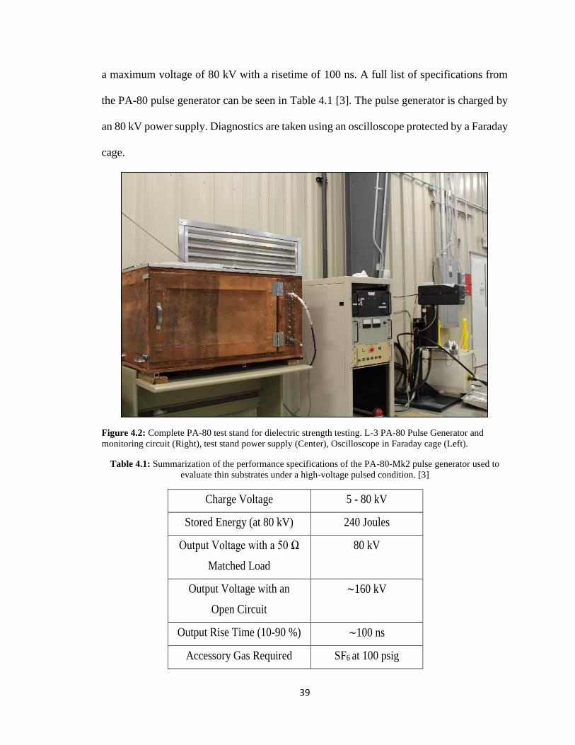
Table 4.1: Summarization of the performance specifications of the PA-80-Mk2 pulse
generator used to evaluate thin substrates under a high-voltage pulsed condition. [3] .....39
Table 6.1: Weibull parameters for all temperature data sets. The bottom row shows the
averaged values to give a general approximation for the entire temperature range. .........79
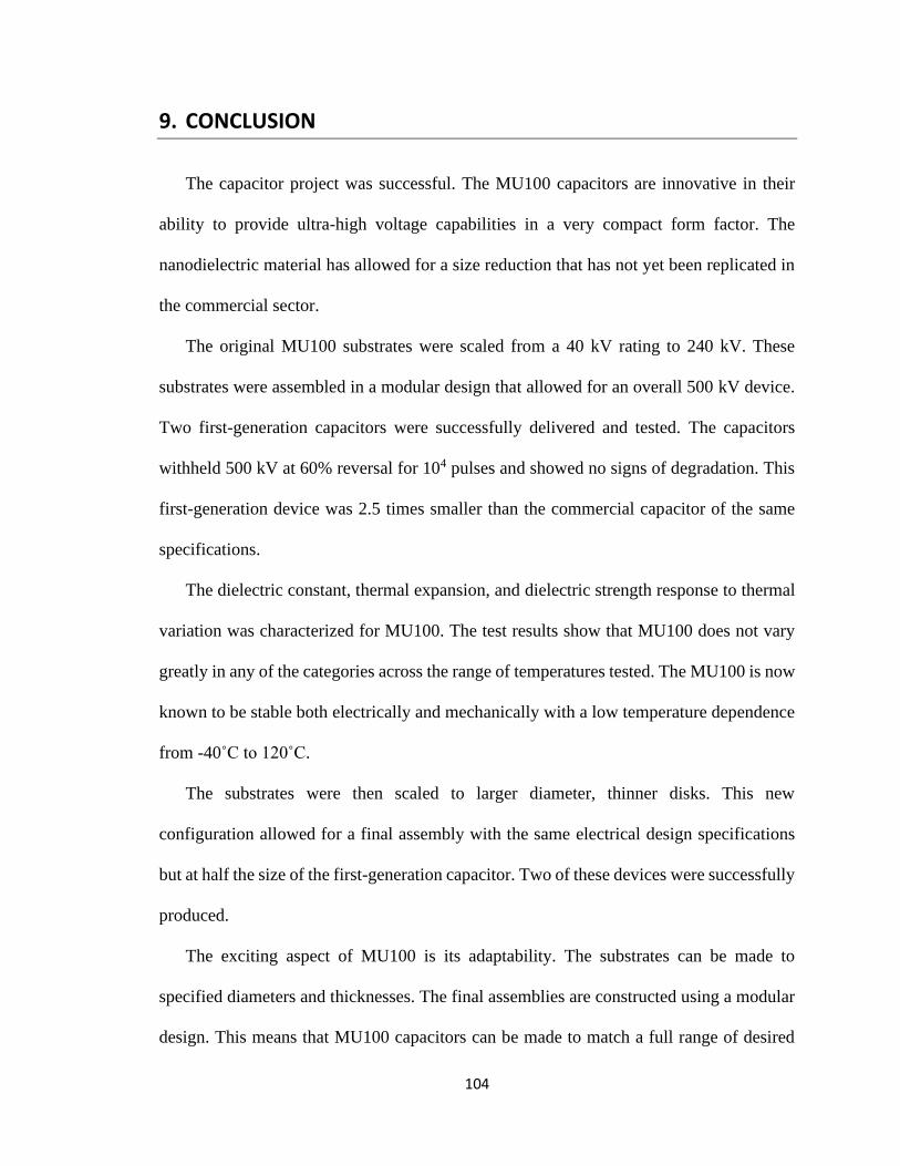
Table 8.1: Volume and weight comparison of GA commercial capacitor and both
generations of MU100 capacitors. The MU100 devices are significantly smaller than the
commercial device. ..........................................................................................................103
Page 7
vi
LIST OF FIGURES
Figure 1.1: Commercially available high voltage polymer film capacitors. Devices
capable of operation well above 100 kV are of most relevance to the scope of this report
[6]. ....................................................................................................................................... 4
Figure 1.2: Energy density versus lifetime of commercial polymer capacitor. Lower
energy density devices possess extremely long lifecycles [6]. ........................................... 5
Figure 1.3: Dielectric strength versus temperature of many common polymers. The
polymers exhibit a steady, constant performance before entering a transition temperature,
beyond that point dielectric strength performance is significantly diminished [9]. ........... 6
Figure 1.4: Diagram showing the typical evolution of the sintering process. If the
necking portion of the sinter is not fully completed a pore will be left behind which will
decrease dielectric strength [14]. ........................................................................................ 8
Figure 1.5: TDK data set of their high voltage ceramic capacitors. The figure shows the
temperature and voltage dependence of capacitance. Capacitance changes continuously
with temperature [11]. ......................................................................................................... 8
Figure 1.6: A small scale MU100 capacitor (right) compared to a commercially available
TDK doorknob capacitor (left), both of which are rated to 40 kV. The MU100 based
devices are considerably smaller. ..................................................................................... 10
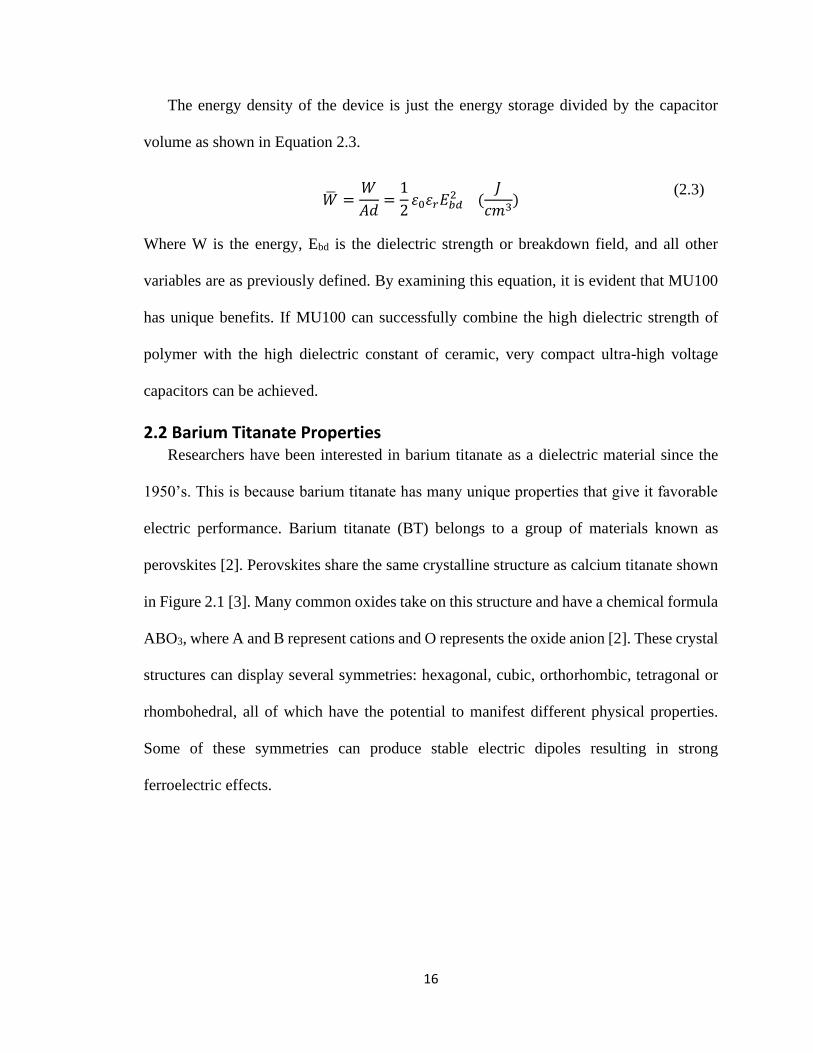
Figure 2.1: A cubic ABO3 perovskite-type unit cell [3]. ................................................. 17
Figure 2.2: The structure change undergone during the cubic phase to tetragonal phase
transition. When the phase change occurs, the cations displace relative to the anion which
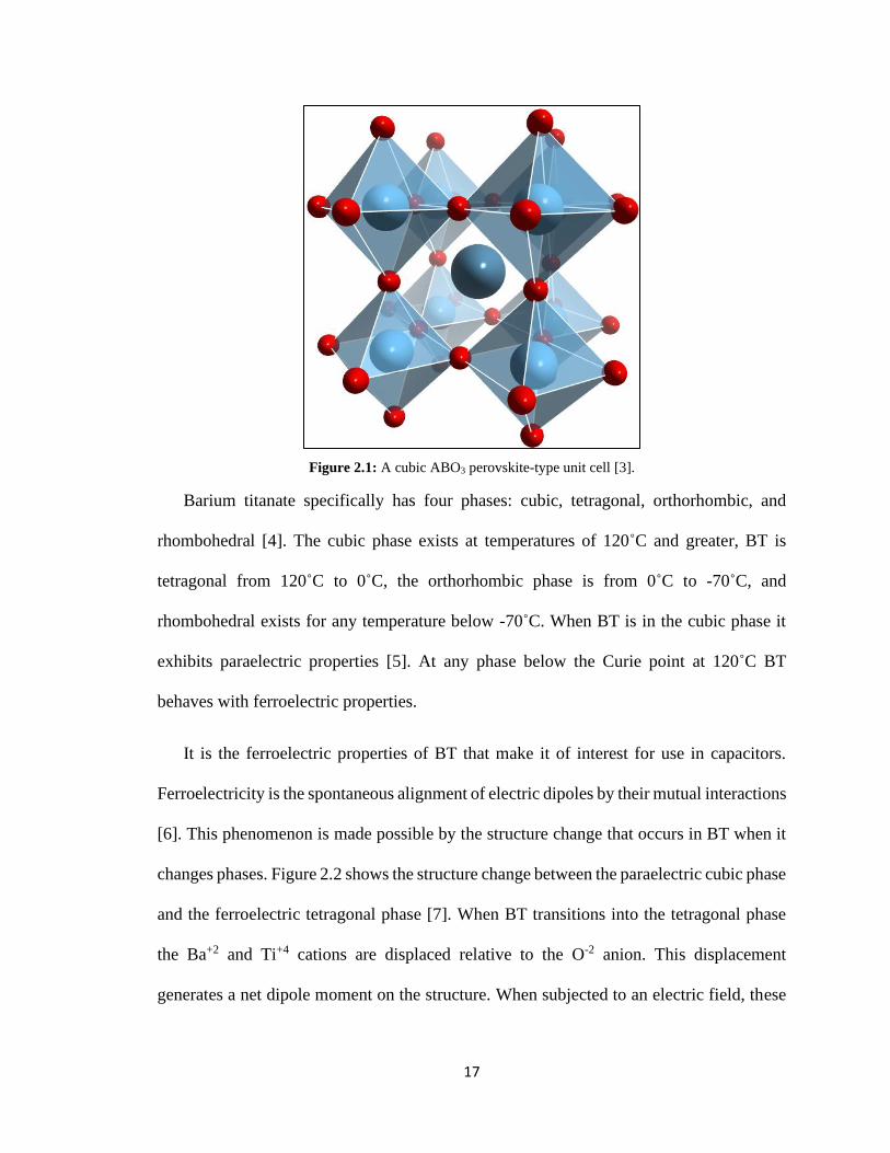
generates a dipole moment [7]. ......................................................................................... 18
Figure 2.3: Relationship of barium titanate grain size to dielectric constant. As grain size
decreases, dielectric constant increases to a maximum point. At the maxima, further size
reduction of grain size results in a reduction of dielectric constant [10]. ......................... 19
Figure 2.4: The relationship of particle size ratios on overall packing density. Some
combination of large and small particles yields the maximum packing density [17]. ...... 20
Figure 2.5: The effect of number of particle sizes on packing density. n is the number of
modes used in the mixture. The ternary and quaternary mixtures have a much higher
maximum packing density compared to the bimodal mixture [19]. ................................. 21
Figure 2.6: Surface-to-volume ratios of nanocomposites as a function of nanoparticle
loading [16]. ...................................................................................................................... 23
Figure 3.1: Complete, sanded and polished MU100 substrate. ....................................... 33
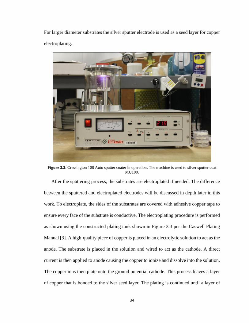
Figure 3.2: Cressington 108 Auto sputter coater in operation. The machine is used to
silver sputter coat MU100. ................................................................................................ 34
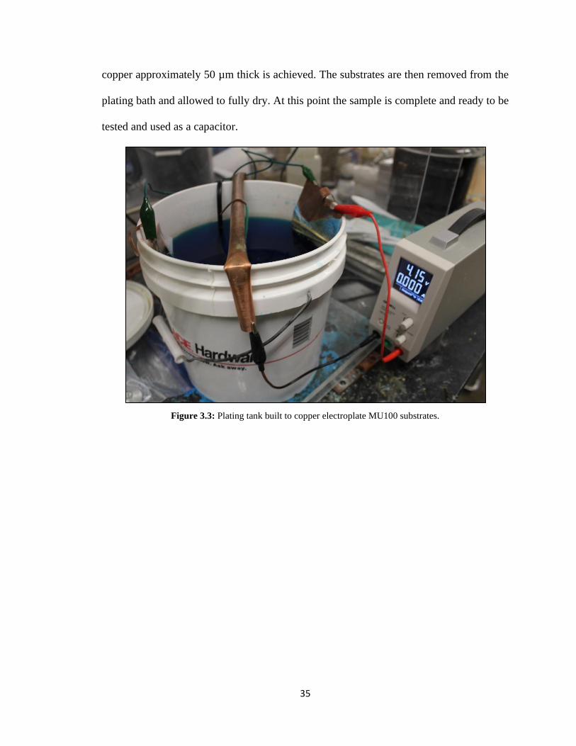
Figure 3.3: Plating tank built to copper electroplate MU100 substrates. ........................ 35
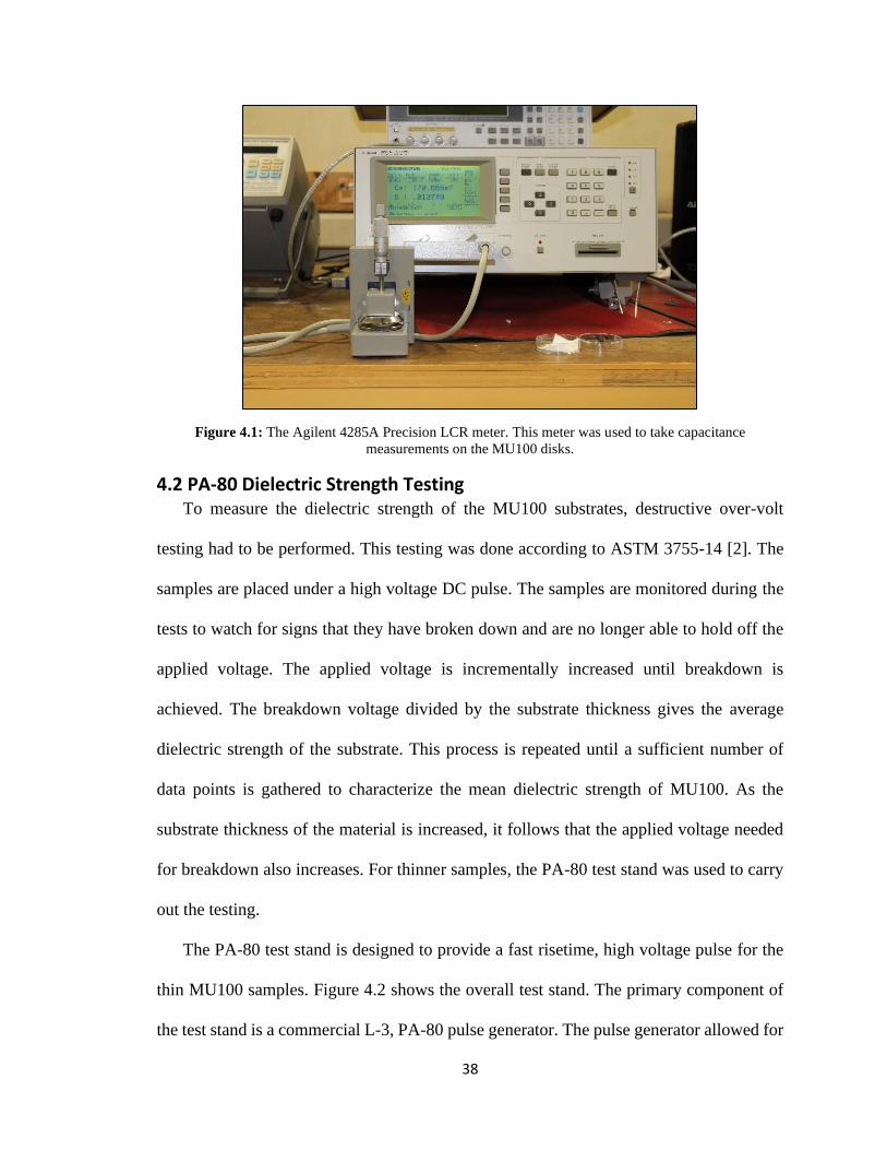
Figure 4.1: The Agilent 4285A Precision LCR meter. This meter was used to take
capacitance measurements on the MU100 disks. ............................................................. 38
Figure 4.2: Complete PA-80 test stand for dielectric strength testing. L-3 PA-80 Pulse
Generator and monitoring circuit (Right), test stand power supply (Center), Oscilloscope
in Faraday cage (Left). ...................................................................................................... 39
Figure 4.3: High voltage probes used to measure voltage across test capacitor. ............. 40
Page 8
vii
Figure 4.4: Typical PA-80 waveform. The traces from both voltage probes can be seen.
........................................................................................................................................... 40
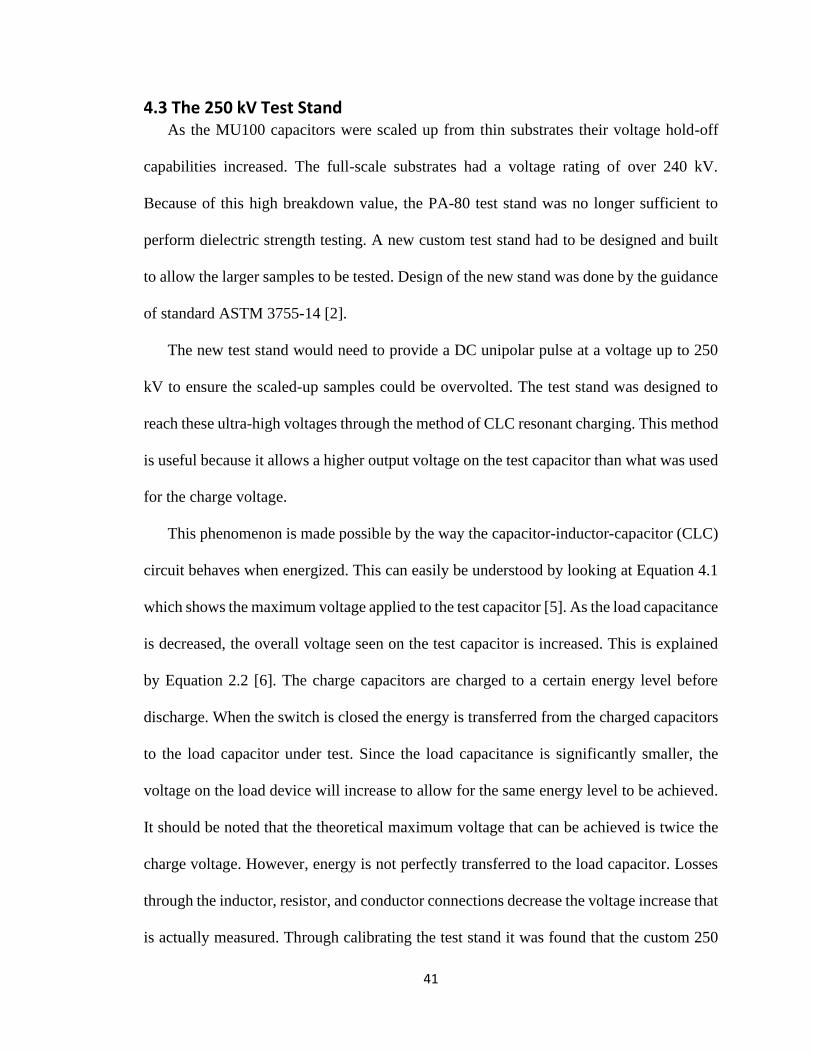
Figure 4.5: Circuit diagram of the 250 kV Test Stand. .................................................... 42
Figure 4.6: Assembled 250 kV test stand. Circuitry is immersed in dielectric oil bath to
prevent flash over. ............................................................................................................. 43
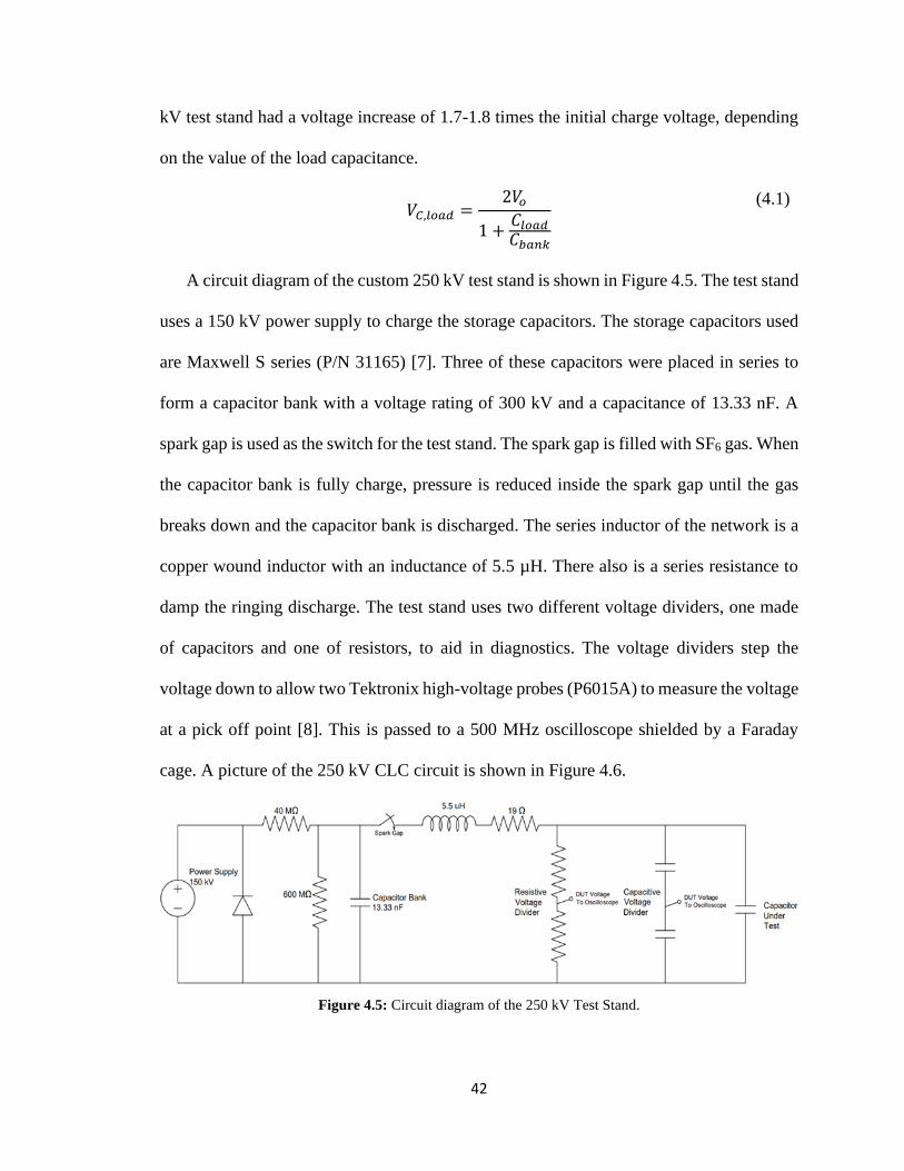
Figure 4.7: A typical waveform from the 250 kV test stand. .......................................... 44
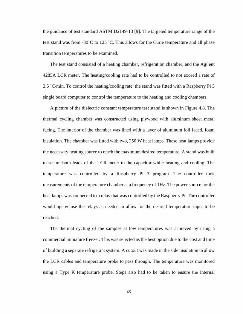
Figure 4.8: Test equipment used to characterize MU100's change in dielectric constant
with temperature. The heating chamber with Raspberry Pi controller (left), the LCR
meter and temperature meter (center), the cooling chamber (right). ................................ 46
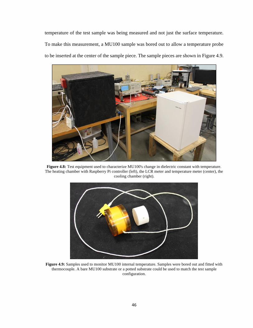
Figure 4.9: Samples used to monitor MU100 internal temperature. Samples were bored
out and fitted with thermocouple. A bare MU100 substrate or a potted substrate could be
used to match the test sample configuration. .................................................................... 46
Figure 4.10: 3-D model of the 250 kV temperature test stand design. A pump would be
used to transfer heated/cooled oil to a sealed test chamber. ............................................. 50
Figure 4.11: A schematic of the heating and cooling system for the temperature test
stand. ................................................................................................................................. 50
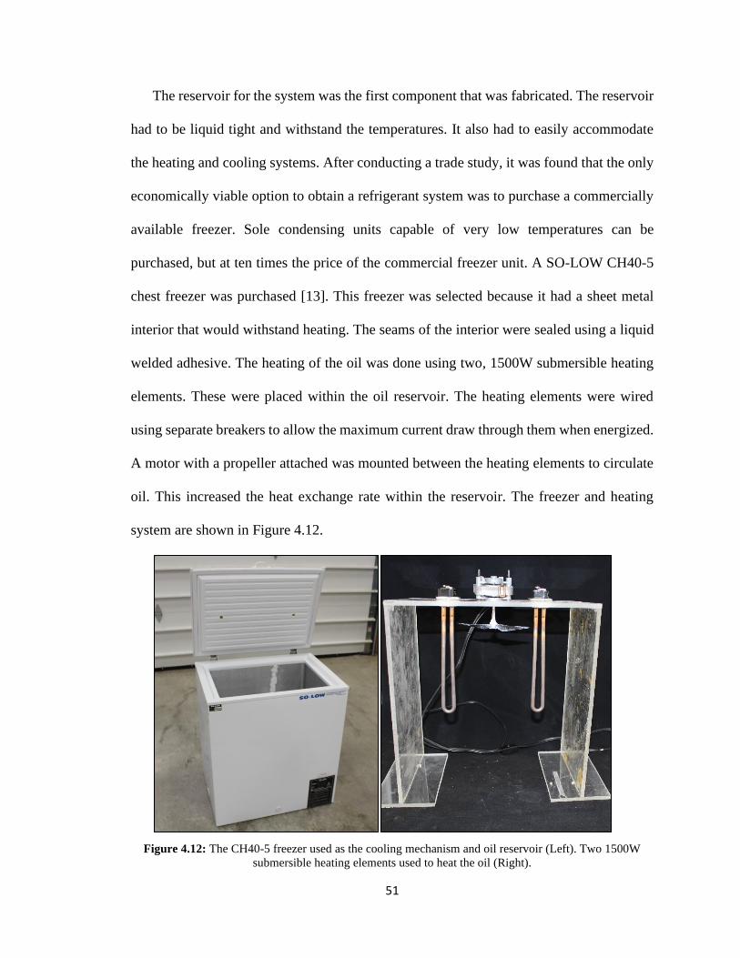
Figure 4.12: The CH40-5 freezer used as the cooling mechanism and oil reservoir (Left).
Two 1500W submersible heating elements used to heat the oil (Right). ......................... 51
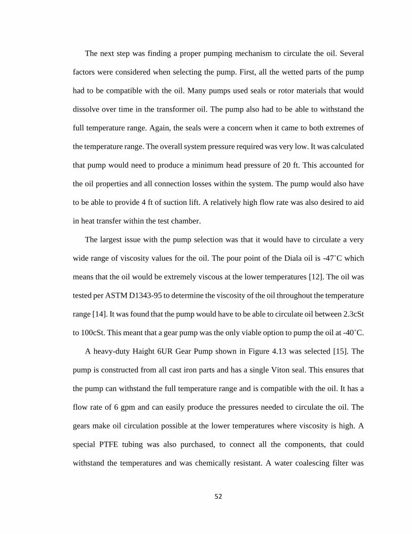
Figure 4.13: Heavy duty gear pump used to circulate oil from reservoir to test chamber.
........................................................................................................................................... 53
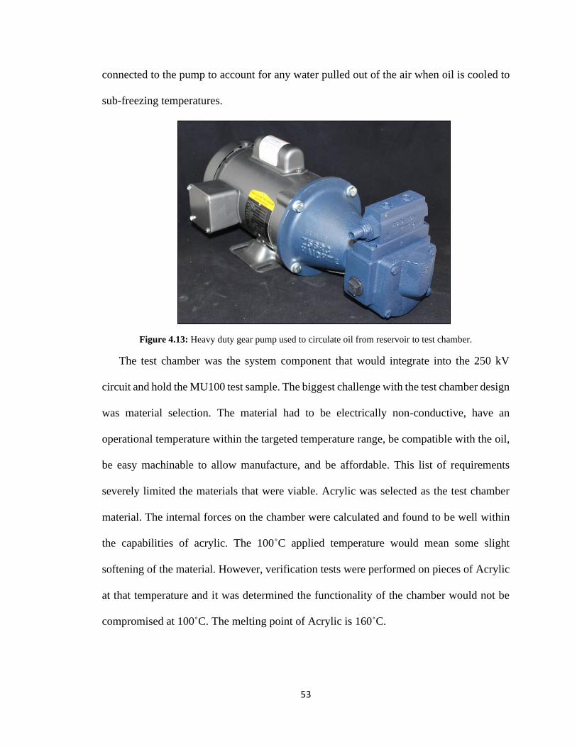
Figure 4.14: High voltage endcap. End cap has a pressure fit electrode stand to secure
the capacitor and provide the test voltage. ........................................................................ 54
Figure 4.15: Completed test chamber. The high voltage end cap is to the right, the
ground end cap to the left.................................................................................................. 55
Figure 4.16: Test stand control set up. A Raspberry Pi program was used to actuate the
relays shown on the right. This controlled the power to the heating, cooling, and pumping
elements. This also served as a safety against overheating the oil. .................................. 56
Figure 4.17: Completed 250 kV temperature test stand. The heating/cooling chamber and
pump above tank (top). The test chamber integrated into the 250 kV test stand (bottom).
........................................................................................................................................... 57
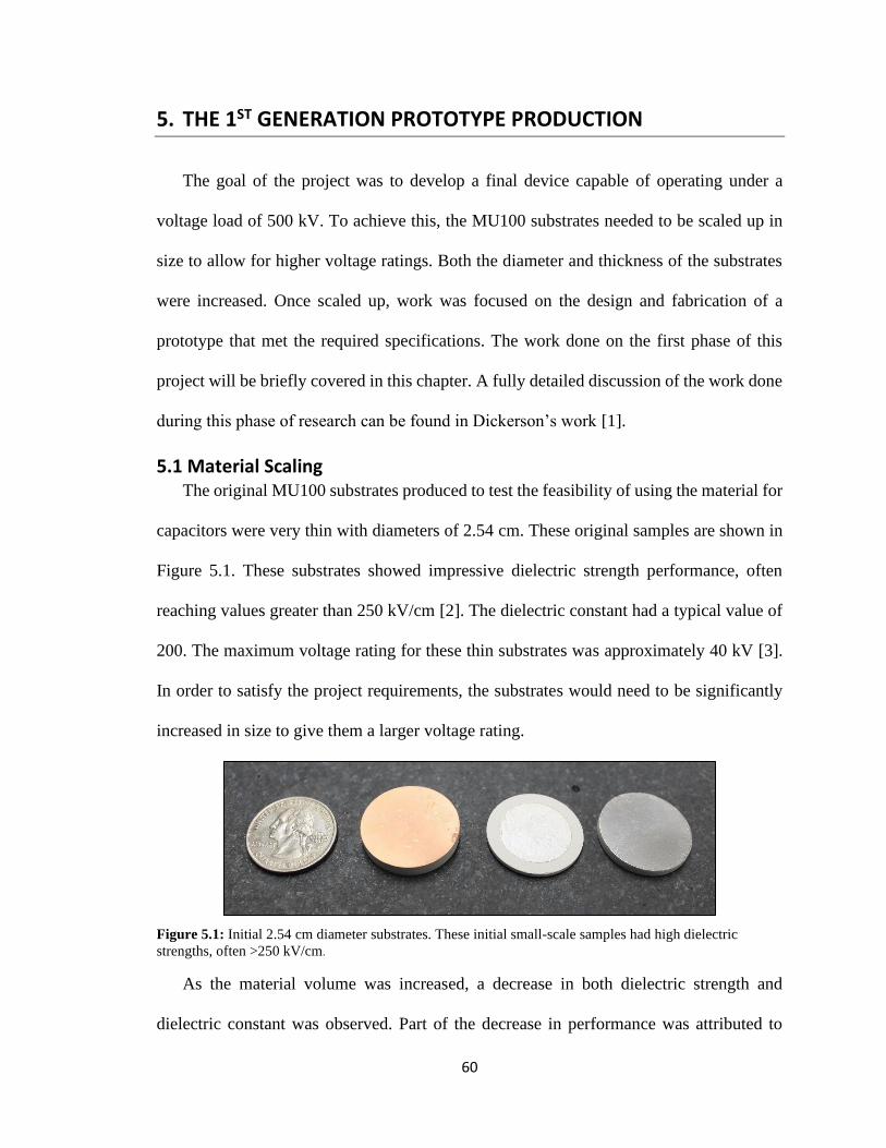
Figure 5.1: Initial 2.54cm diameter substrates. These initial small-scale samples had high
dielectric strengths, often >250 kV/cm. ............................................................................ 60
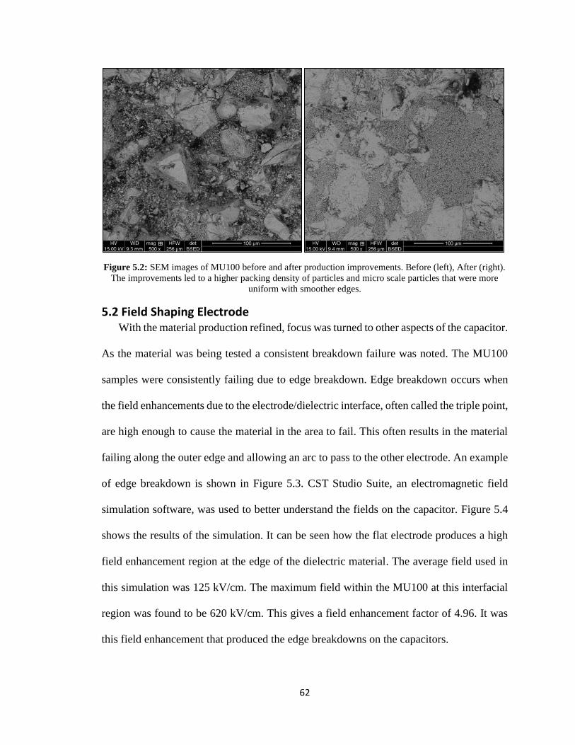
Figure 5.2: SEM images of MU100 before and after production improvements. Before
(left), After (right). The improvements led to a higher packing density of particles and
micro scale particles that were more uniform with smoother edges. ................................ 62
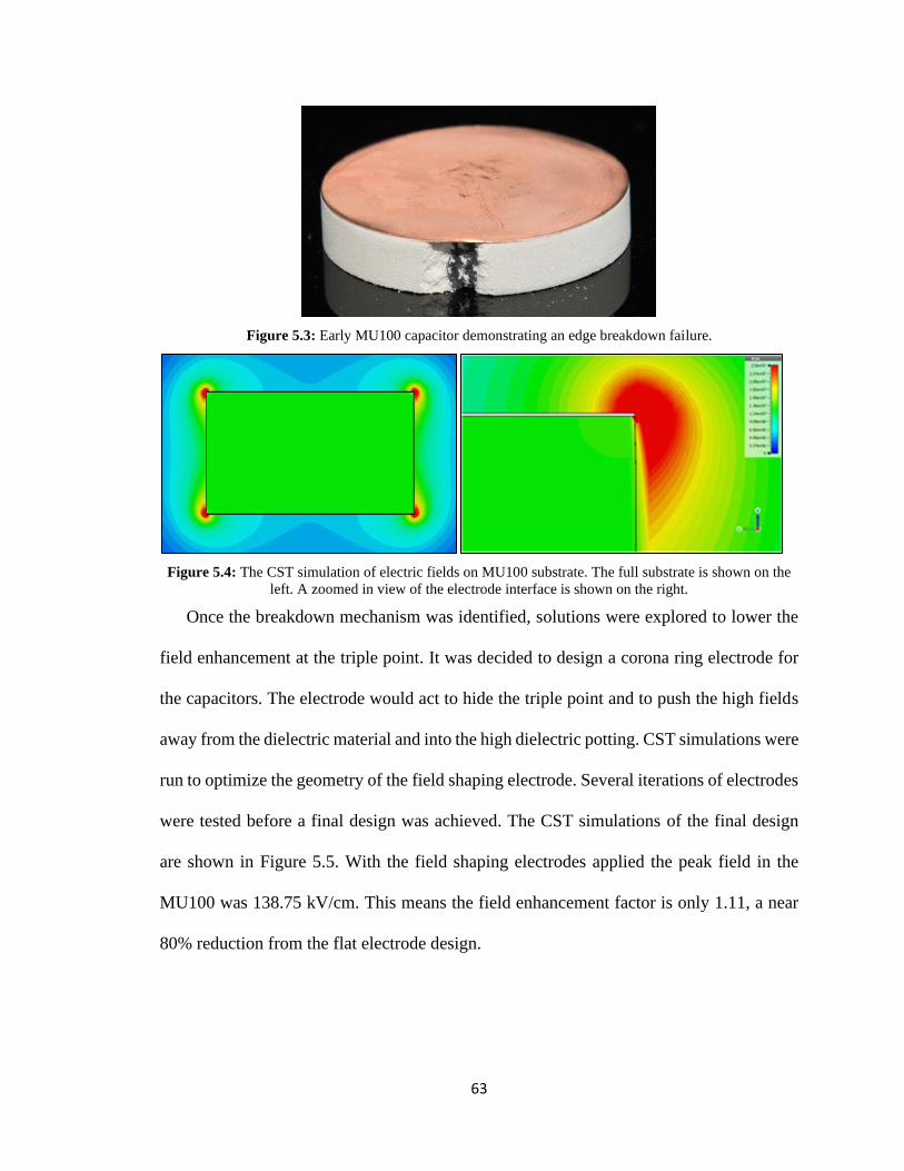
Figure 5.3: Early MU100 capacitor demonstrating an edge breakdown failure. ............. 63
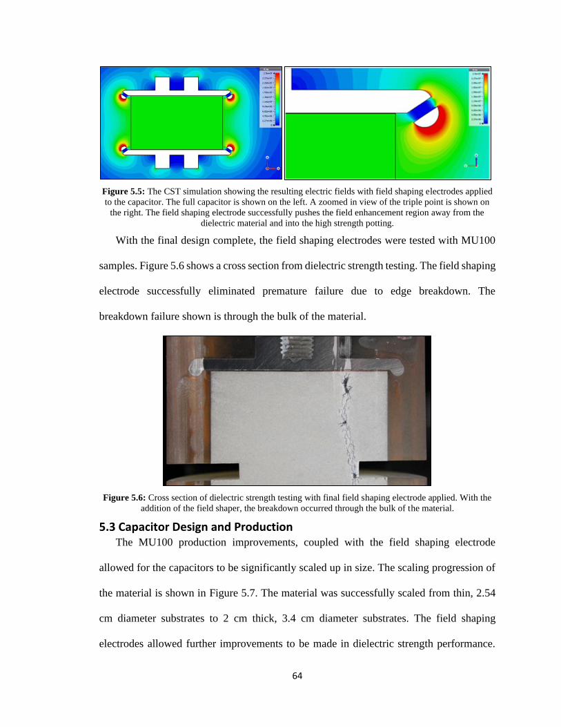
Figure 5.4: The CST simulation of electric fields on MU100 substrate. The full substrate
is shown on the left. A zoomed in view of the electrode interface is shown on the right. 63
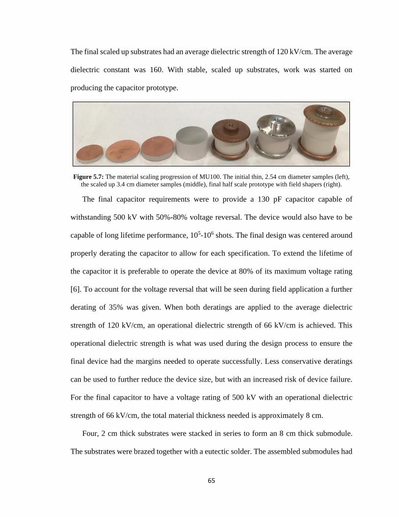
Figure 5.5: The CST simulation showing the resulting electric fields with field shaping
electrodes applied to the capacitor. The full capacitor is shown on the left. A zoomed in
view of the triple point is shown on the right. The field shaping electrode successfully
pushes the field enhancement region away from the dielectric material and into the high
strength potting. ................................................................................................................ 64
Page 9
viii
Figure 5.6: Cross section of dielectric strength testing with final field shaping electrode
applied. With the addition of the field shaper, the breakdown occurred through the bulk
of the material. .................................................................................................................. 64
Figure 5.7: The material scaling progression of MU100. The initial thin, 2.54cm
diameter samples (left), the scaled up 3.4cm diameter samples (middle), final half scale
prototype with field shapers (right)................................................................................... 65
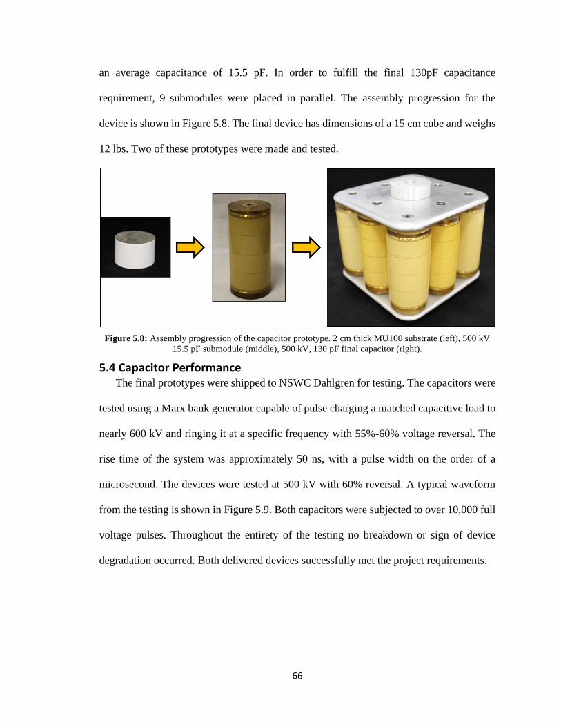
Figure 5.8: Assembly progression of the capacitor prototype. 2cm thick MU100
substrate (left), 500 kV 15.5pF submodule (middle), 500 kV, 130 pF final capacitor
(right). ............................................................................................................................... 66
Figure 5.9: Typical waveform from full voltage capacitor testing. The device was
subjected to a minimum of 500 kV with a voltage reversal of approximately 60%. ........ 67
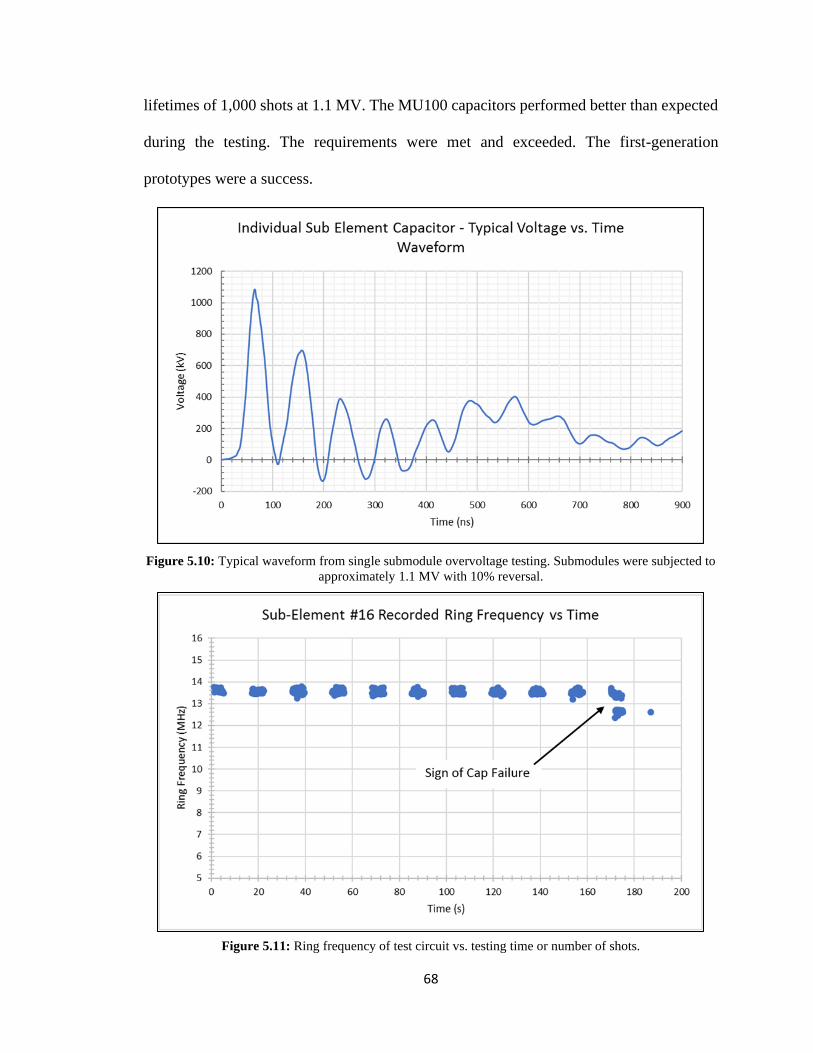
Figure 5.10: Typical waveform from single submodule overvoltage testing. Submodules
were subjected to approximately 1.1 MV with 10% reversal. .......................................... 68
Figure 5.11: Ring frequency of test circuit vs. testing time or number of shots.............. 68
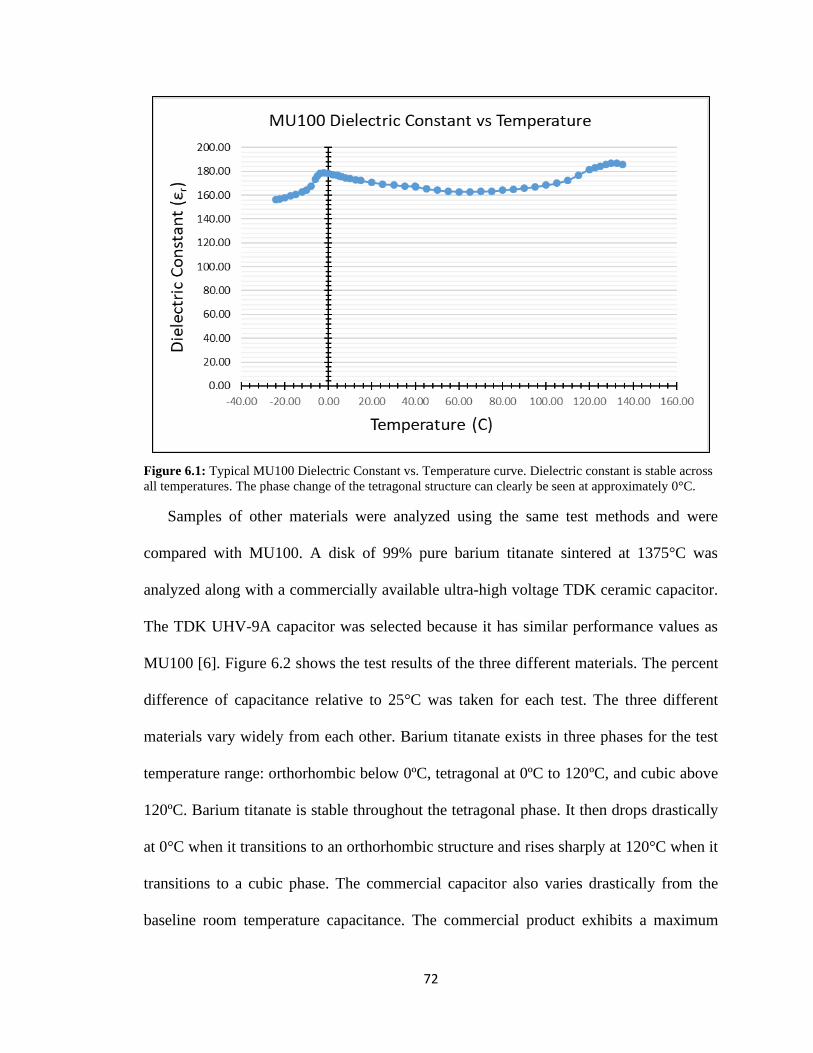
Figure 6.1: Typical MU100 Dielectric Constant vs. Temperature curve. Dielectric
constant is stable across all temperatures. The phase change of the tetragonal structure
can clearly be seen at approximately 0°C. ........................................................................ 72
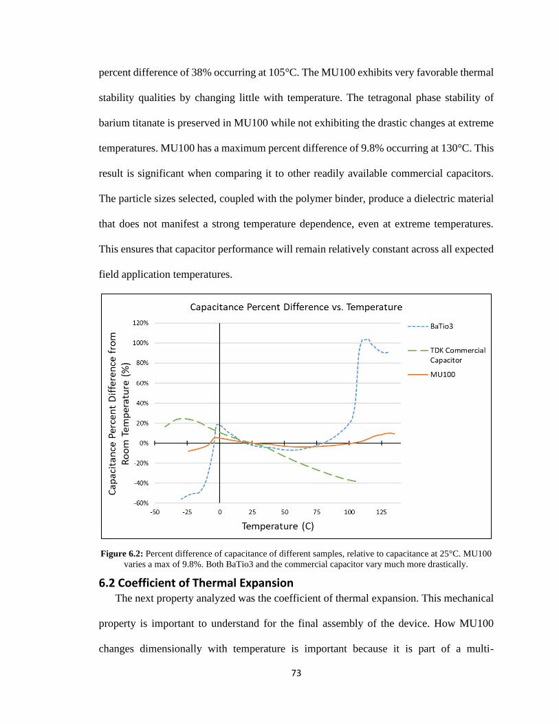
Figure 6.2: Percent difference of capacitance of different samples, relative to capacitance
at 25°C. MU100 varies a max of 9.8%. Both BaTio3 and the commercial capacitor vary
much more drastically. ...................................................................................................... 73
Figure 6.3: Three different materials analyzed during thermal expansion tests. High
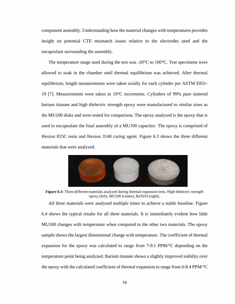
dielectric strength epoxy (left), MU100 (center), BaTiO3 (right). ................................... 74
Figure 6.4: Relative change of sample length vs. temperature. MU100 shows minor
dimension change across a wide range of temperatures. .................................................. 75
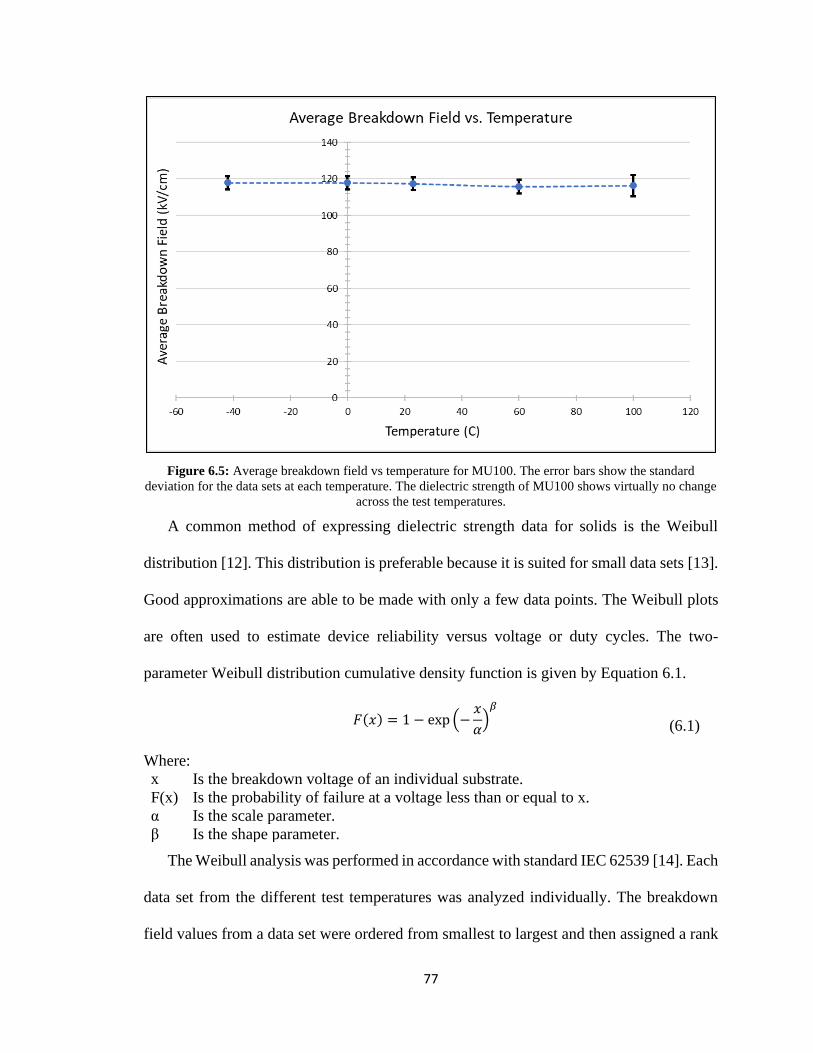
Figure 6.5: Average breakdown field vs temperature for MU100. The error bars show
the standard deviation for the data sets at each temperature. The dielectric strength of
MU100 shows virtually no change across the test temperatures. ..................................... 77
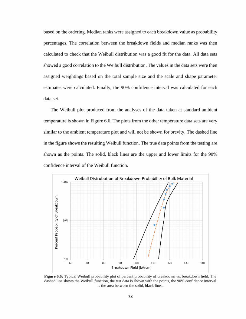
Figure 6.6: Typical Weibull probability plot of percent probability of breakdown vs.
breakdown field. The dashed line shows the Weibull function, the test data is shown with
the points, the 90% confidence interval is the area between the solid, black lines. ......... 78
Figure 6.7: Typical MU100 samples used during dielectric strength vs temperature
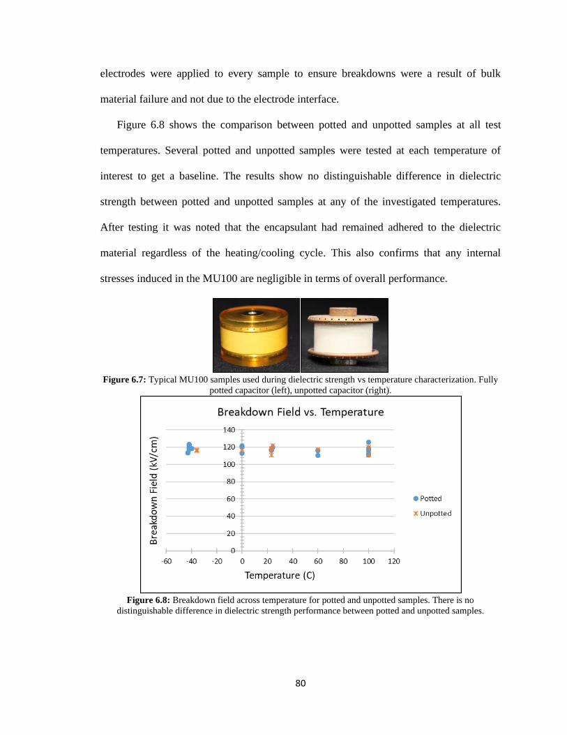
characterization. Fully potted capacitor (left), unpotted capacitor (right). ....................... 80
Figure 6.8: Breakdown field across temperature for potted and unpotted samples. There
is no distinguishable difference in dielectric strength performance between potted and
unpotted samples. .............................................................................................................. 80
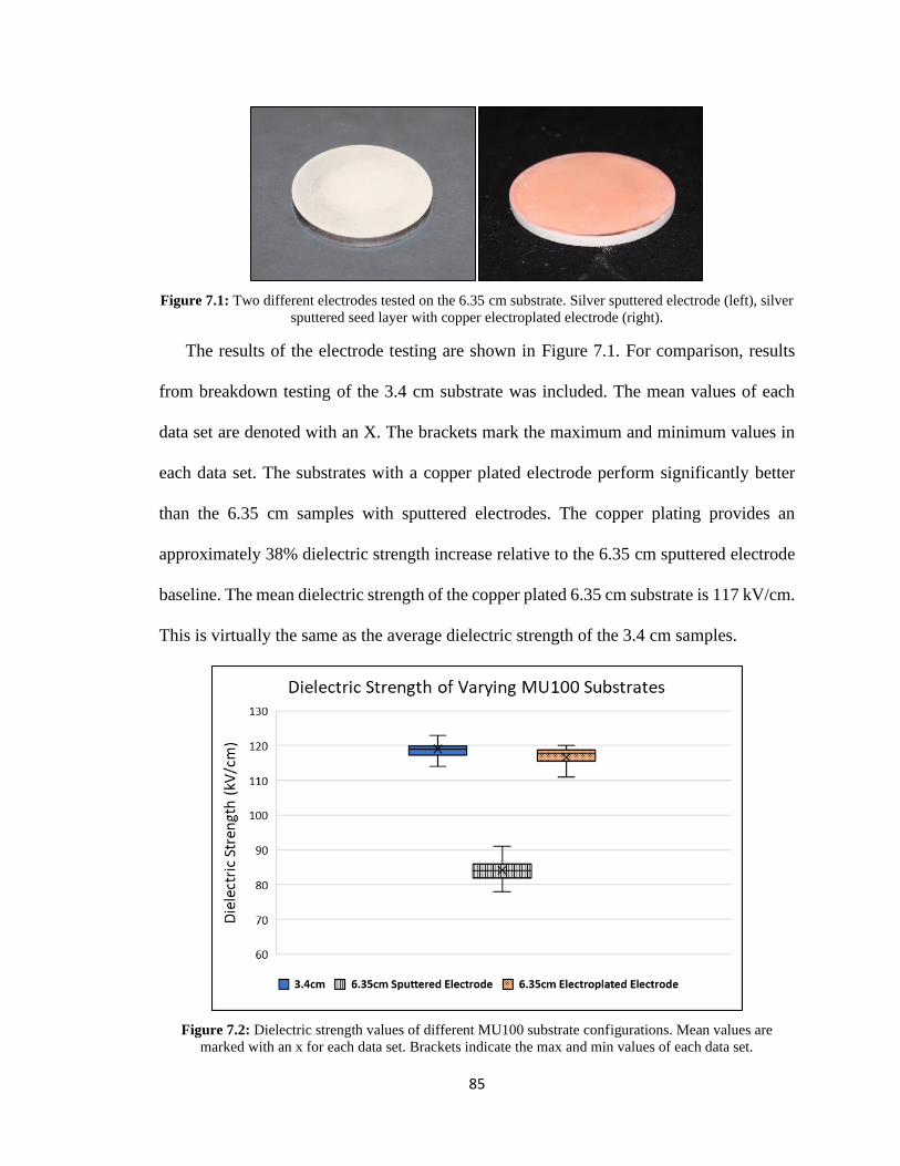
Figure 7.1: Two different electrodes tested on the 6.35 cm substrate. Silver sputtered
electrode (left), silver sputtered seed layer with copper electroplated electrode (right). .. 85
Figure 7.2: Dielectric strength values of different MU100 substrate configurations. Mean
values are marked with an x for each data set. Brackets indicate the max and min values
of each data set. ................................................................................................................. 85
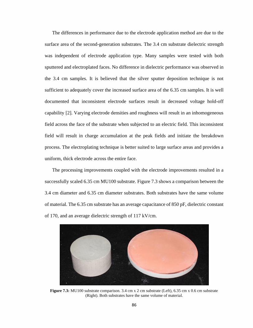
Figure 7.3: MU100 substrate comparison. 3.4 cm x 2 cm substrate (Left), 6.35 cm x 0.6
cm substrate (Right). Both substrates have the same volume of material. ....................... 86
Page 10
ix
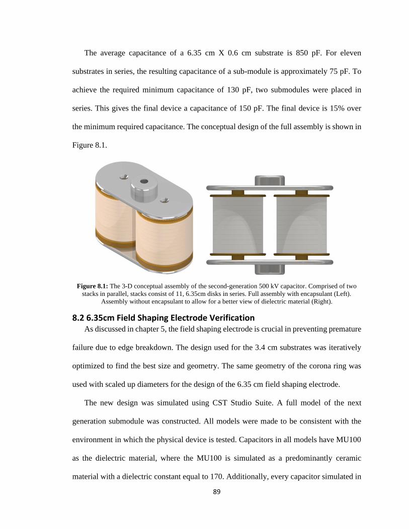
Figure 8.1: The 3-D conceptual assembly of the second-generation 500 kV capacitor.
Comprised of two stacks in parallel, stacks consist of 11, 6.35cm disks in series. Full
assembly with encapsulant (Left). Assembly without encapsulant to allow for a better
view of dielectric material (Right). ................................................................................... 89
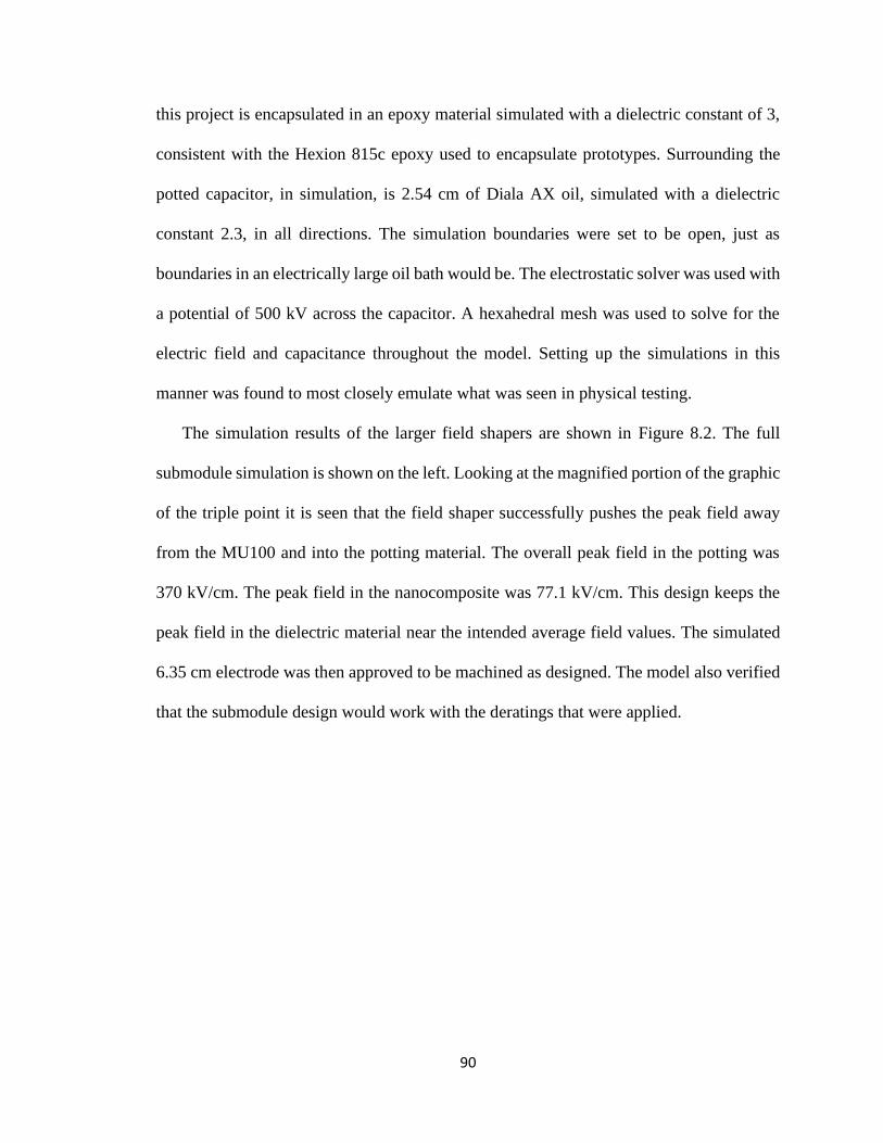
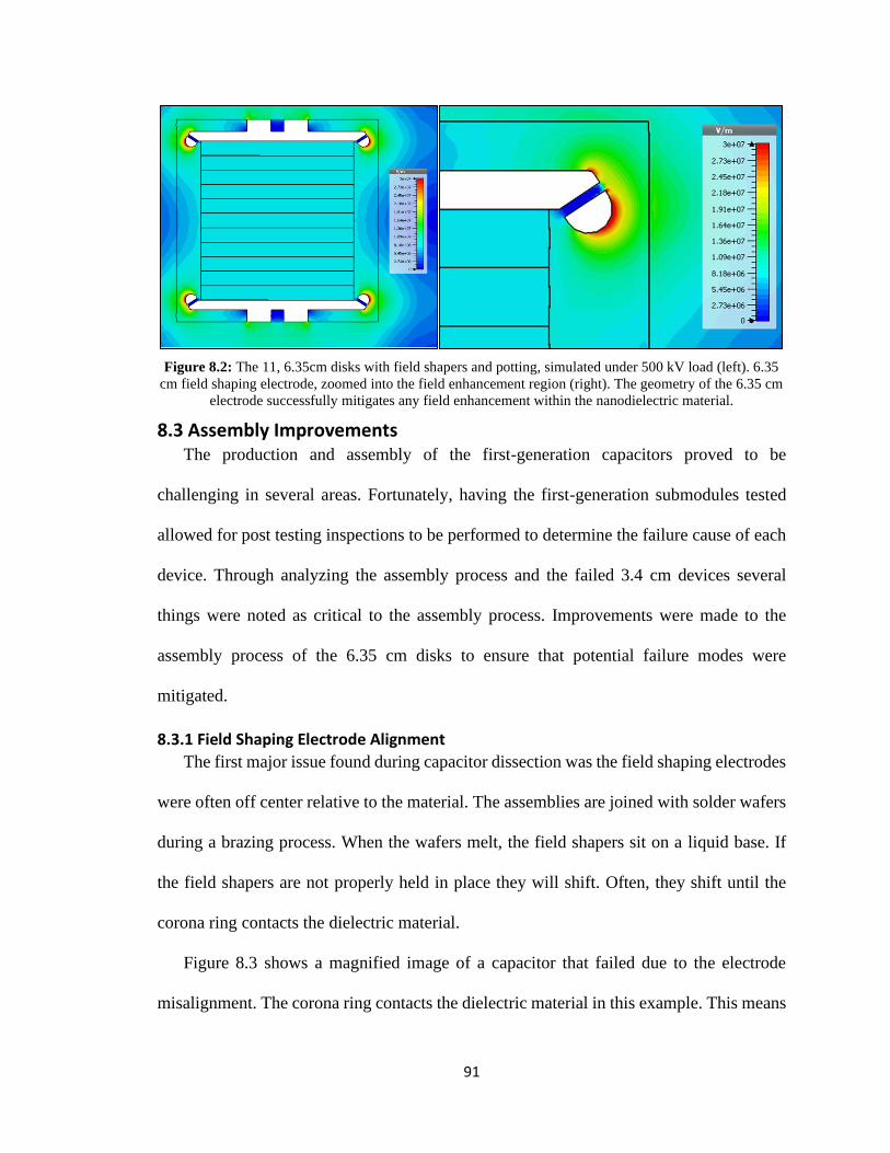
Figure 8.2: The 11, 6.35cm disks with field shapers and potting, simulated under 500 kV
load (left). 6.35 cm field shaping electrode, zoomed into the field enhancement region
(right). The geometry of the 6.35 cm electrode successfully mitigates any field
enhancement within the nanodielectric material. .............................................................. 91
Figure 8.3: A MU100 failure due to misaligned field shaper. Corona ring is touching the
dielectric material, causing higher peak fields than intended within the dielectric. ......... 92
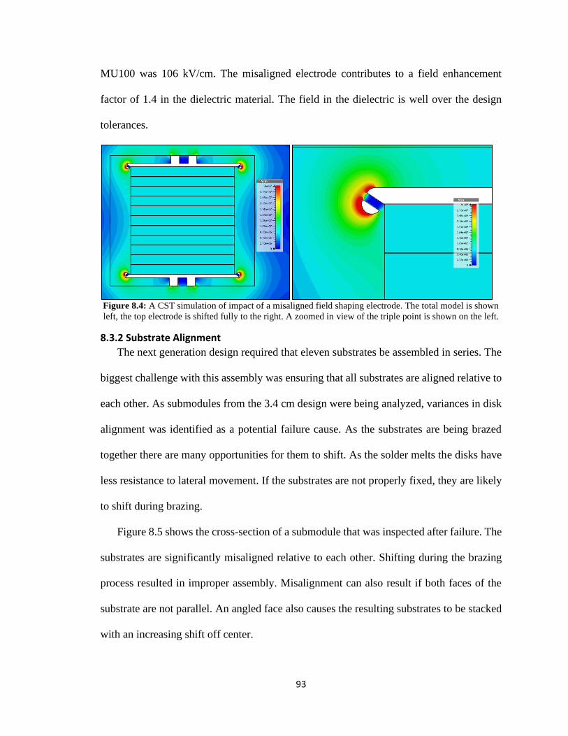
Figure 8.4: A CST simulation of impact of a misaligned field shaping electrode. The
total model is shown left, the top electrode is shifted fully to the right. A zoomed in view
of the triple point is shown on the left. ............................................................................. 93
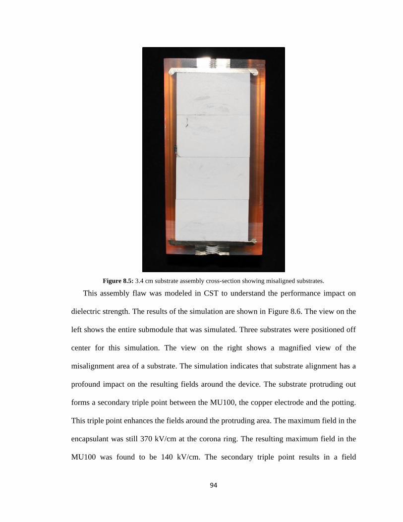
Figure 8.5: 3.4cm substrate assembly cross-section showing misaligned substrates. ..... 94
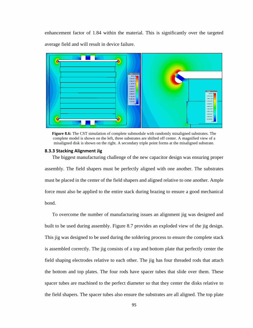
Figure 8.6: The CST simulation of complete submodule with randomly misaligned
substrates. The complete model is shown on the left, three substrates are shifted off
center. A magnified view of a misaligned disk is shown on the right. A secondary triple
point forms at the misaligned substrate. ........................................................................... 95
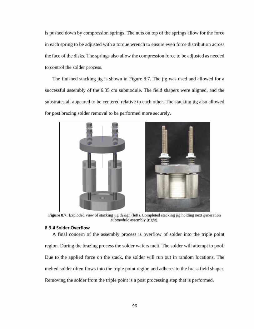
Figure 8.7: Exploded view of stacking jig design (left). Completed stacking jig holding
next generation submodule assembly (right). ................................................................... 96
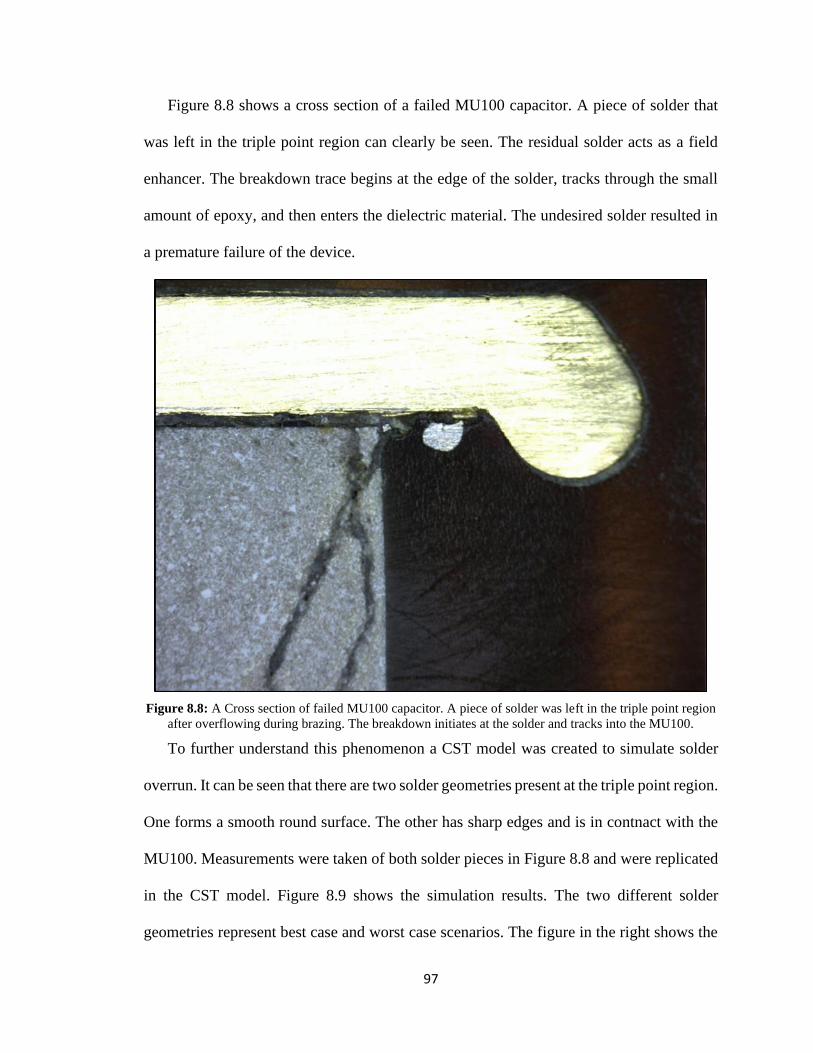
Figure 8.8: A Cross section of failed MU100 capacitor. A piece of solder was left in the
triple point region after overflowing during brazing. The breakdown initiates at the solder
and tracks into the MU100. ............................................................................................... 97
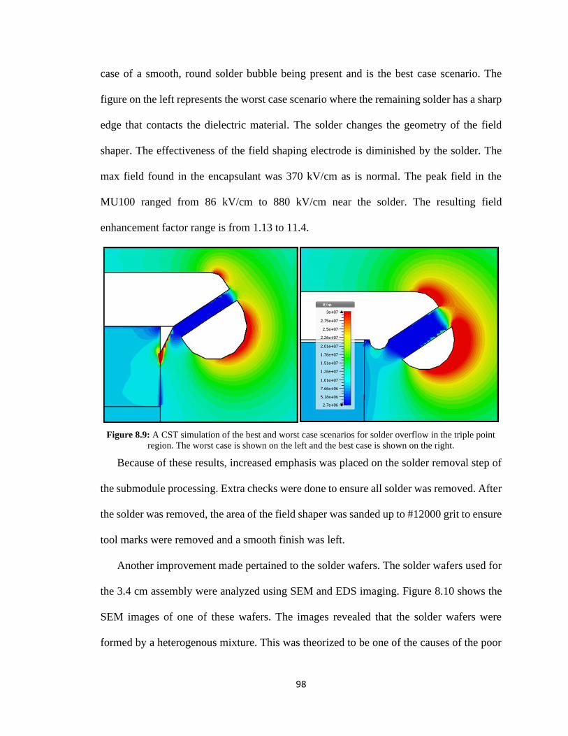
Figure 8.9 A CST simulation of the best and worst case scenarios for solder overflow in
the triple point region. The worst case is shown on the left and the best case is shown on
the right. ............................................................................................................................ 98
Figure 8.10: SEM image (left) and EDS image (right) of old solder wafer. The wafer is
comprised of a heterogenous mixture, this can lead to issues of the mechanical bond
between the substrates during brazing. ............................................................................. 99
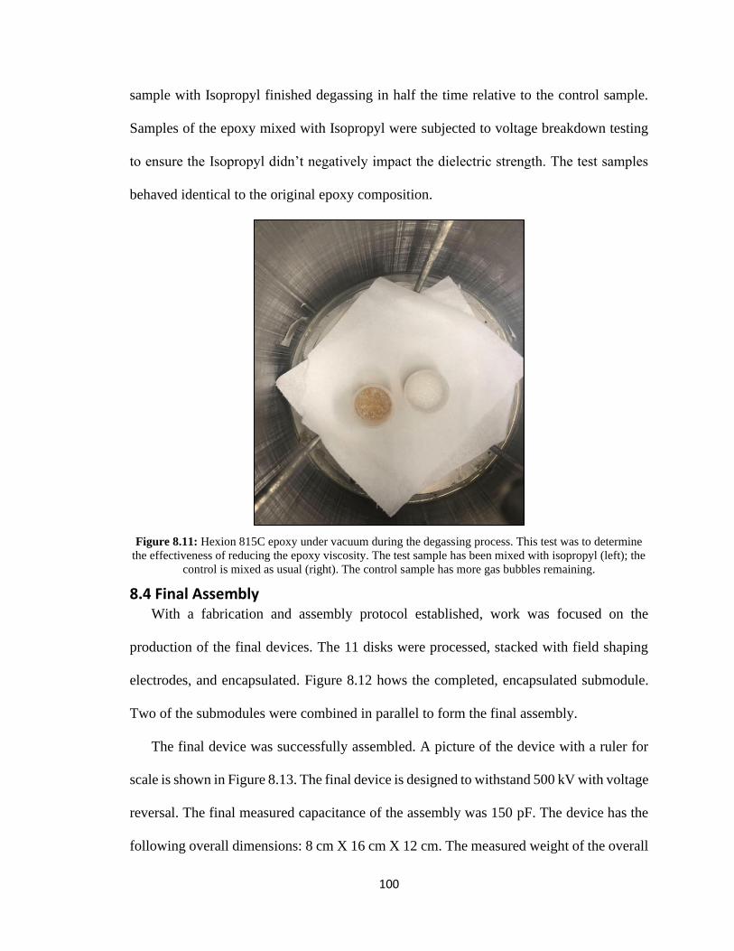
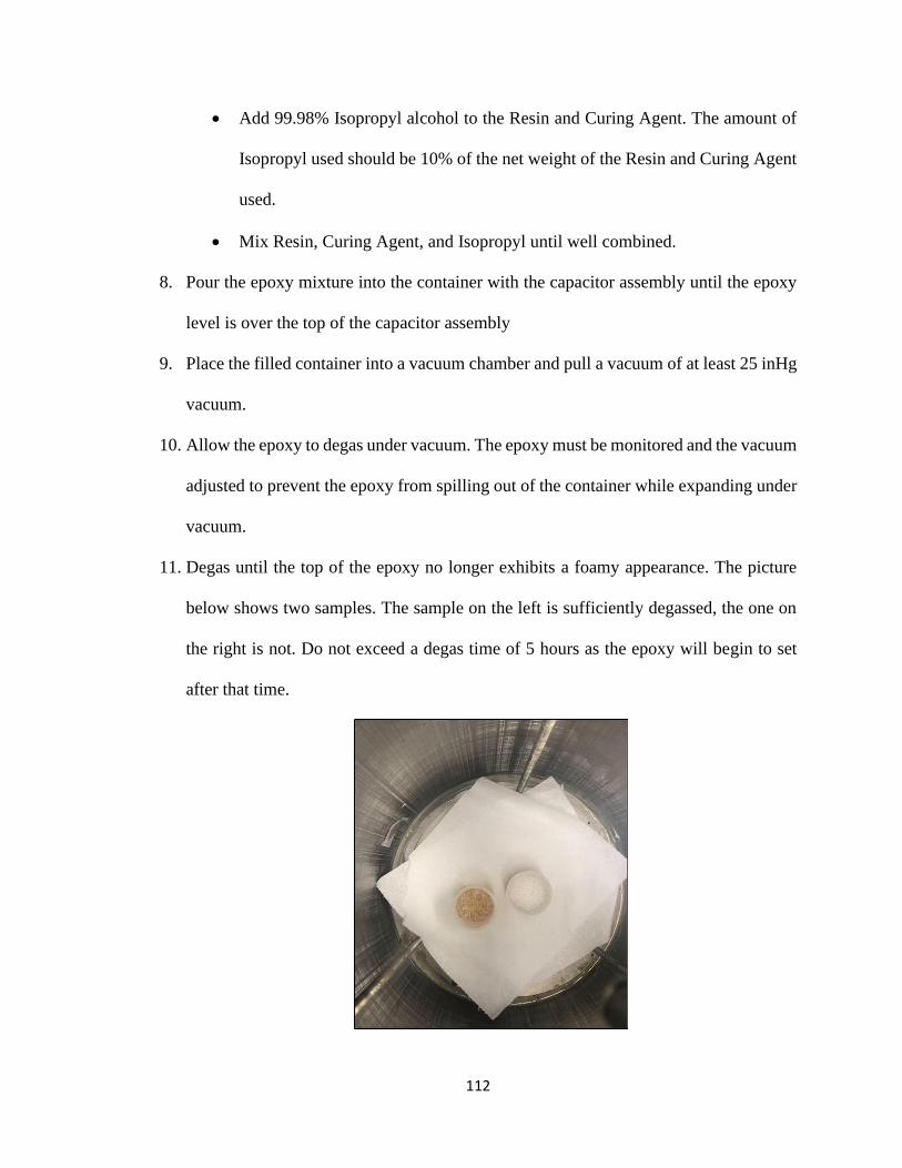
Figure 8.11: Hexion 815C epoxy under vacuum during the degassing process. This test
was to determine the effectiveness of reducing the epoxy viscosity. The test sample has
been mixed with isopropyl (left); the control is mixed as usual (right). The control sample
has more gas bubbles remaining. .................................................................................... 100
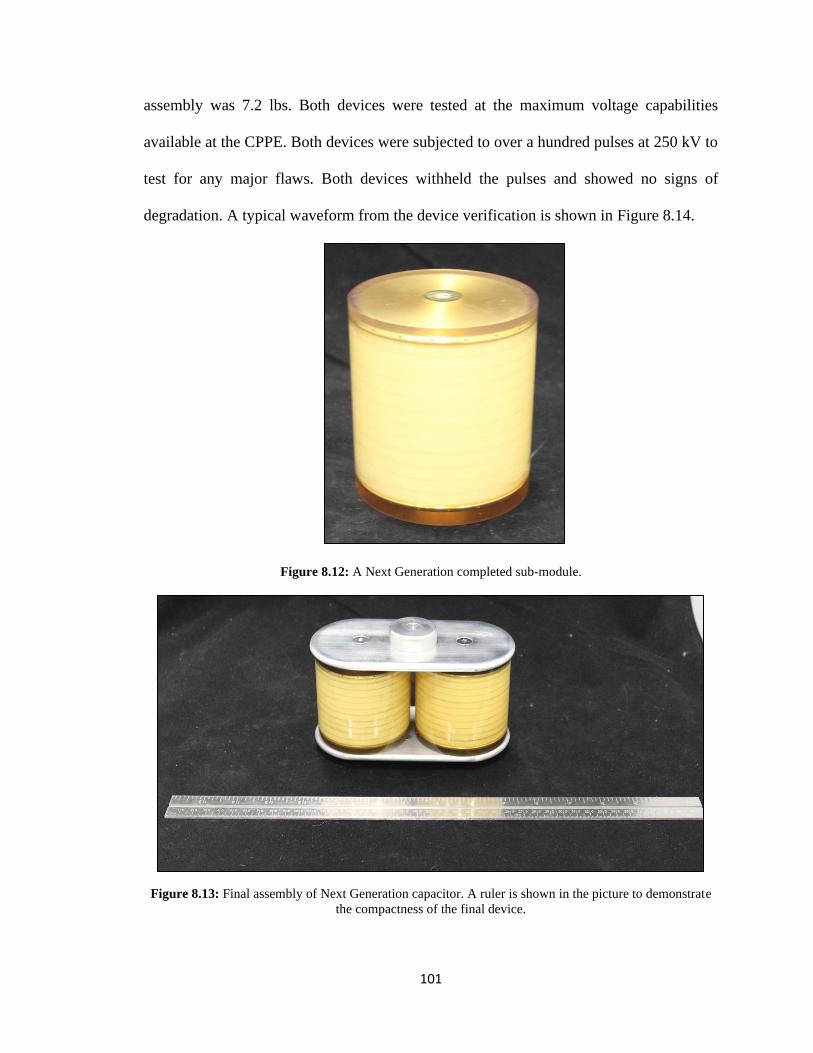
Figure 8.12: A Next Generation completed sub-module. .............................................. 101
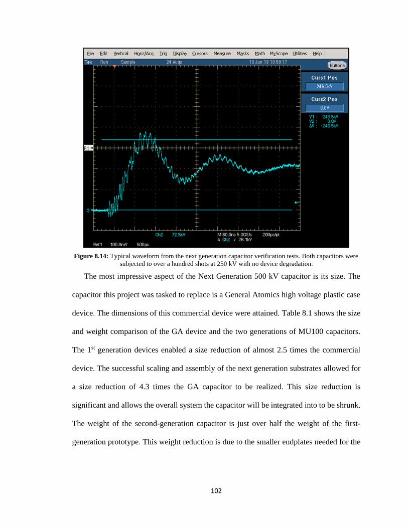
Figure 8.13: Final assembly of Next Generation capacitor. A ruler is shown in the picture
to demonstrate the compactness of the final device. ....................................................... 101
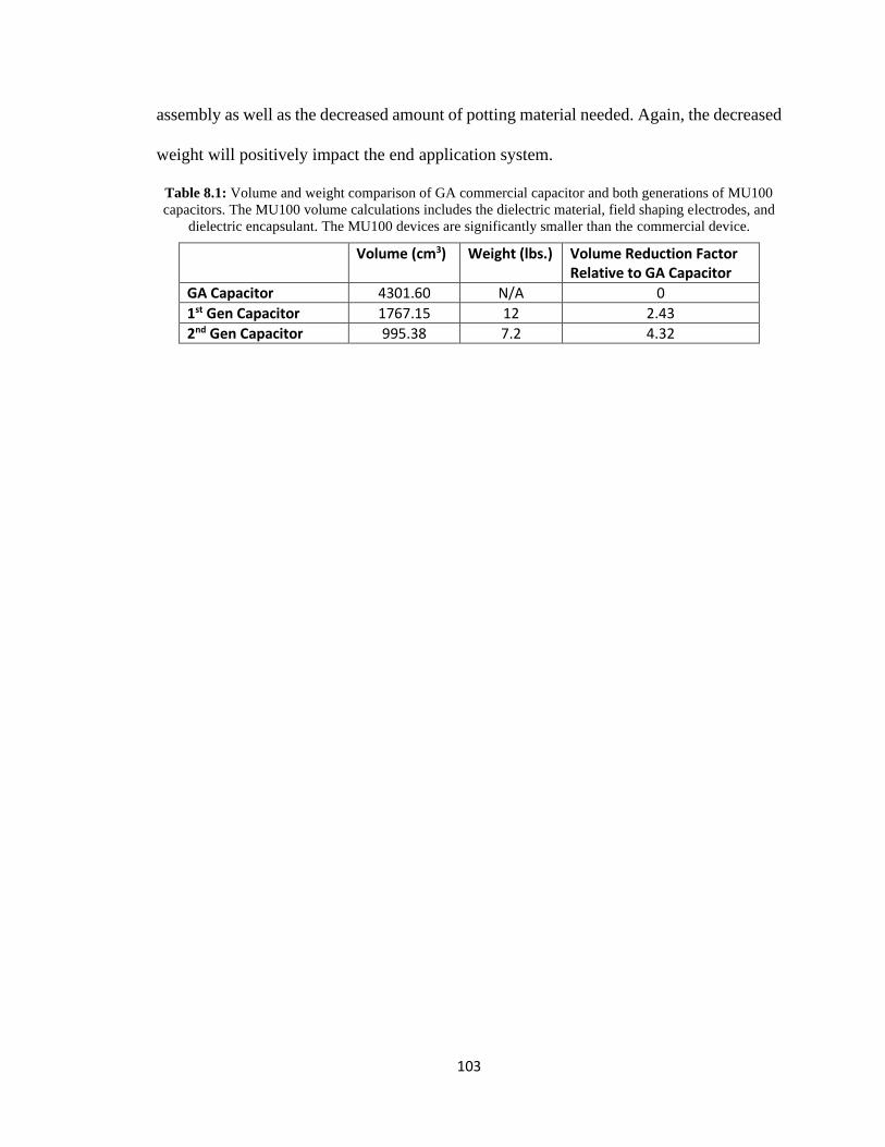
Figure 8.14: Typical waveform from the next generation capacitor verification tests.
Both capacitors were subjected to over a hundred shots at 250 kV with no device
degradation. ..................................................................................................................... 102
Page 11
x
ABSTRACT The University of Missouri has been developing compact capacitors for use in high
voltage, pulsed power and directed energy applications. The capacitors are made from a
proprietary nanodielectric, MU100, which is a polymer-ceramic composite composed of
nanoceramic barium titanate and a proprietary binding agent. MU100 exhibits several
novel qualities including high dielectric strength along with facile machining and assembly
characteristics.
The material was successfully used to fabricate capacitor prototypes capable of
repeatable performance at 500 kV with lifetimes greater than 104 shots. These initial
prototypes were smaller than comparable commercial devices by a factor of 2.5.
The dielectric constant, thermal expansion, and dielectric strength were measured for
MU100 from -40ºC to 120ºC. The results demonstrate the nanodielectric has a strong
stability both electrically and mechanically across the entire temperature test range. The
maximum capacitance percent difference of MU100 relevant to standard temperature was
9.8% occurring at 130ºC. The maximum linear coefficient of thermal expansion found was
1.5 PPM/ºC. The dielectric strength was found to show virtually no change with
temperature.
The MU100 substrates were then scaled to a diameter of 6.35 cm to allow for further
size reduction of the final capacitor. With a 6.35 cm diameter design, a volume reduction
of over 4 times, relative to commercial capacitors, was achieved while maintaining the
same electrical performance as the first-generation device.
The theory, methodologies, and results for characterizing and producing these
capacitors is discussed in this work.
Page 12
1
1. INTRODUCTION
1.1 Current State of Capacitors Capacitors are an important component to virtually all electrical systems. This is
particularly true in the pulsed power and directed energy fields. Due to the high-power
systems typically found in these areas, the capacitors used tend to be large and heavy. This
is because, in order to withstand the applied field and operate at the desired specifications,
the capacitors must be significantly de-rated in voltage holdoff. As a result, a large portion
of the overall system size and weight can be attributed to the capacitors within that system.
Decreasing size and weight of pulsed power systems is a chief concern for systems to
operate effectively in the field. It follows then that shrinking the size of capacitors currently
available is of great interest to those working within this research area.
Dielectric capacitors are the most common type of capacitor in use today because of
their preferable dielectric properties, availability, and low cost [1]. There are two types of
dielectric capacitors, polymer capacitors and ceramic capacitors [2]. Polymer capacitors
tend to have extremely high dielectric strength values. However, they suffer from having
low dielectric constant values, typically between values of 2-5 [3]. Ceramic capacitors
demonstrate the opposite behavior. Ceramic capacitors are known to have high dielectric
constant values but relatively low dielectric strength. It is because of this that specific
applications dictate which capacitor type is used. These two types of capacitors will be
further analyzed in this chapter.
In order to produce new devices with higher energy densities, a material with high
dielectric strength and high dielectric constant is required. This is problematic because it is
generally understood that dielectric strength is inversely proportional to dielectric constant.
Page 13
2
McPherson suggests the following relationship to describe the behavior of the two
properties [4].
𝐸𝑏𝑑~(𝑘)−
12
(1.1)
Where E is the breakdown field and k is the dielectric constant. In order to account for this,
much work is currently being done to combine polymers and ceramics to form composite
capacitors. The idea of polymer-composite capacitors is to combine the high dielectric
strength polymer and the high dielectric constant ceramic to get a final device with
favorable values in both properties. The Center for Physical and Power Electronics (CPPE)
at the University of Missouri has been developing a polymer-ceramic material with this
goal in mind. The later chapters of this work will cover the development, characterization,
and performance of that composite material.
1.1.1 Current State of Polymer Film Capacitors
Polymer materials employed in capacitors tend to have very high dielectric strengths
with very low dielectric constant values. Table 1.1 lists the dielectric constant values for
the most common polymers found in polymer thin film capacitors. Note that most of the
values are very low. The primary advantage of polymers is that they exhibit very high
dielectric strength performance. Because of this, sheets of polymers can be manufactured
with very thin dimensions. Polymer capacitors are typically manufactured by wrapping
large surface areas of thin polymer film with conductive foil [5]. Large surface areas are
required to achieve appreciable capacitance. As a result, the size of polymer capacitors can
be significant if higher capacitance values are required.
Page 14
3
Table 1.1: List of dielectric permittivities of polymers commonly used in capacitors [3].
Polymer Dielectric Permittivity
Nonfluorinated aromatic polyimides 3.2-3.6
Fluorinated polyimide 2.6-2.8
Poly(phenyl quinoxaline) 2.8
Poly(arylene ether oxazole) 2.6-2.8
Poly(arylene ether) 2.9
Polyquinoline 2.8
Silsesquioxane 2.8-3.0
Poly(norborene) 2.4
Perfluorocyclobutane polyether 2.4
Fluorinated poly(arylene ether) 2.7
Polynaphthalene 2.2
Poly(tetrafluoroethylene) 1.9
Polystyrene 2.6
Poly(vinylidene fluoride-co-hexafluoropropylene) ~12
Poly(ether ketone ketone) ~3.5
Polymer capacitors are perhaps the most common capacitor type commercially
available. Many companies focus on manufacturing these devices. There are few however
that manufacture for the ultra-high voltage regime where this work is focused. One of the
leading producers of ultra-high voltage polymer capacitors is General Atomics (GA). They
produce high voltage polymer film capacitors over a wide range of specifications, ranging
from 100 mF at 1 kV to 10’s of pF at 2 MV [6]. General Atomics will be used as the
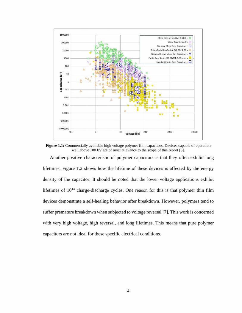
commercial baseline standard when comparisons are made throughout this work. Figure
1.1 shows the performance of General Atomics full catalog of polymer capacitors. This
work is only concerned with voltages well over 100 kV. As such, GA’s plastic case series
is what the CPPE has sought to outperform. It can be seen that capacitance decreases
linearly with an increase in voltage load.
Page 15
4
Figure 1.1: Commercially available high voltage polymer film capacitors. Devices capable of operation
well above 100 kV are of most relevance to the scope of this report [6].
Another positive characteristic of polymer capacitors is that they often exhibit long
lifetimes. Figure 1.2 shows how the lifetime of these devices is affected by the energy
density of the capacitor. It should be noted that the lower voltage applications exhibit
lifetimes of 1014 charge-discharge cycles. One reason for this is that polymer thin film
devices demonstrate a self-healing behavior after breakdown. However, polymers tend to
suffer premature breakdown when subjected to voltage reversal [7]. This work is concerned
with very high voltage, high reversal, and long lifetimes. This means that pure polymer
capacitors are not ideal for these specific electrical conditions.
Page 16
5
Figure 1.2: Energy density versus lifetime of commercial polymer capacitor. Lower energy density devices
possess extremely long lifecycles [6].
Polymer capacitors also vary in their performance under different thermal conditions.
The primary cause of failure due to temperature is due to a polymer being heated past its
glass transition temperature [8]. When a polymer is heated, its free electrons gain mobility.
At the glass transition temperature, the mobility of the free electrons becomes great enough
that they can move along the free path length of the binder. As these electrons accelerate
along the free path, they can displace other free electrons resulting in an avalanche
breakdown condition. Due to this, many polymers demonstrate a constant dielectric
strength up to a certain temperature and then show a drastic decrease in dielectric strength
as temperature is further increased. Figure 1.3 shows the dielectric strength of many
common polymers as temperature varies [9]. It can be seen that there is typically a constant
dielectric strength regardless of temperature. At some point, the temperature of the polymer
Page 17
6
is raised enough to allow the electrons free mobility. At this point the dielectric strength is
drastically reduced for all higher temperatures.
Figure 1.3: Dielectric strength versus temperature of many common polymers. The polymers exhibit a
steady, constant performance before entering a transition temperature, beyond that point dielectric strength
performance is significantly diminished [9].
Currently polymers are the most accessible form of dielectric capacitor. They are
affordable and readily available. They have high dielectric strengths which make them
preferable for high voltage applications. They also are easy to manufacture and process.
They have extremely long lifetimes, especially at lower voltage operation. However, they
suffer from extremely low dielectric constant values and must have large form factors when
significant capacitance values are required. The frequency of the application is
significantly limited by their inherent geometry.
Page 18
7
1.1.2 Current State of Ceramic Capacitors
Pure ceramic devices are the other primary type of dielectric capacitor. These
capacitors are less common than the polymer capacitors and are still an emerging
technology. The advantage of ceramic materials is that they possess high dielectric constant
values. Barium titanate for example has a dielectric constant that is three orders of
magnitude greater than polymers [10]. The disadvantage of ceramics is that typically have
poor dielectric strengths. As a result, ceramic capacitor applications are often limited to
lower voltage applications relative to polymer capacitors. Low voltage ceramic capacitors
are often utilized in circuit designs, because of their high dielectric values they are able to
be manufactured in smaller form factors relative to polymer capacitors of the same
specifications.
Because of their poor performance in the multiple kilovolt regime, only a few
companies are producing very high voltage ceramic capacitors. TDK is the leading
company for commercially available high voltage ceramic capacitors. They currently
produce a capacitor with a max rating of 50 kV [11]. The primary reason ceramic materials
suffer from low dielectric strength can be explained with how they are manufactured.
Ceramic particles are pressed together to form a loosely bound bulk material known as a
green body block. This green body is then sintered at high heat for a specified time. During
the sintering process the grain boundaries will meld together. Once sintered, electrodes are
applied to the ceramic material to form the final capacitor. During this process it is possible
for pores to form within the sintered material. These pores will be filled with air and will
act as a breakdown initiation point when subjected to an electric field [12]. Another issue
is that the grain boundaries will not fully combine and will allow an easier conductive path
Page 19
8
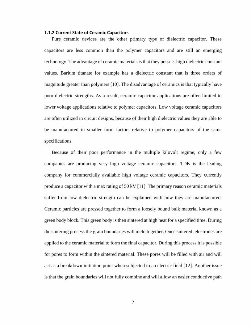
through the material [13]. Figure 1.4 shows a graphic of how voids can form during the
sintering process [14].
Figure 1.4: Diagram showing the typical evolution of the sintering process. If the necking portion of the
sinter is not fully completed a pore will be left behind which will decrease dielectric strength [14].
Another characteristic of pure ceramic capacitors is that their electrical properties can
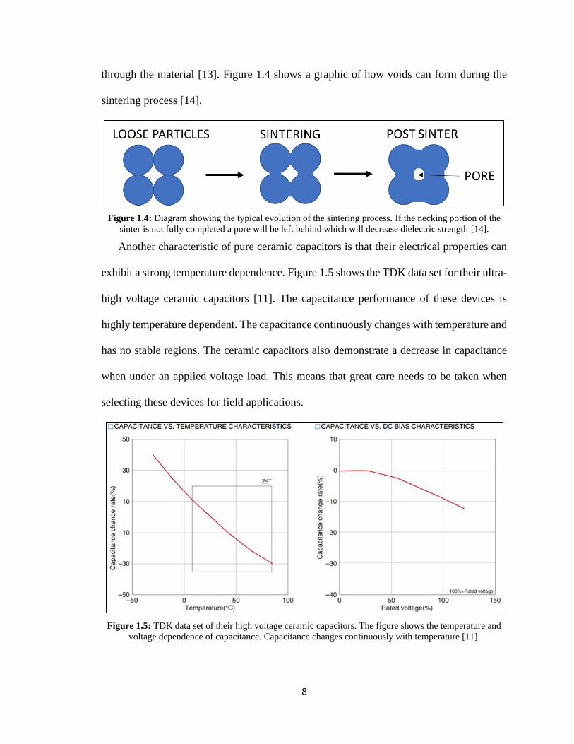
exhibit a strong temperature dependence. Figure 1.5 shows the TDK data set for their ultra-
high voltage ceramic capacitors [11]. The capacitance performance of these devices is
highly temperature dependent. The capacitance continuously changes with temperature and
has no stable regions. The ceramic capacitors also demonstrate a decrease in capacitance
when under an applied voltage load. This means that great care needs to be taken when
selecting these devices for field applications.
Figure 1.5: TDK data set of their high voltage ceramic capacitors. The figure shows the temperature and
voltage dependence of capacitance. Capacitance changes continuously with temperature [11].
Page 20
9
Sintered ceramic devices can also be difficult to manufacture and assemble. Ceramics
in general present unique issues when processing or machining is required. They tend to
be hard and brittle [15]. This means that post sintering processing can be very complicated
and is often unsuccessful. Special tools and fixtures may be required which adds cost,
complications, and opportunity for flaw introduction during the assembly.
Ceramic dielectric capacitors are a field of research that continues to mature. They have
high dielectric constant performance. Due to this they can often be assembled into very
compact final devices. However, because of their low dielectric strengths they are often
limited to lower energy density applications. They also are difficult to machine and can
exhibit strong temperature dependence for electrical properties. These devices perform
well in specific applications but may be limited for general field applications.
1.2 CPPE Previous Work For the past several years the CPPE at the University of Missouri has sought to make
advancements in the field of dielectric materials. The center has done this by developing a
polymer-ceramic nanocomposite named MU100. The MU100 was originally developed
for the purpose of shrinking high power antennas using dielectric loading [16]. The
material derives its name from the fact that it has a dielectric constant of 100 at frequencies
of 1 GHz. The composite was designed to be easily machinable to allow for complex
antenna geometries to be produced. The material was found to have favorable dielectric
constant, dielectric strength, machineability, and thermal stability. Because of these
attributes it was decided that MU100 would be a good material candidate for producing
compact high voltage capacitors [17] [18].
Initial efforts to produce capacitors with MU100 were focused around small scale
samples. The initial small-scale samples had a diameter of 2.54 cm and were typically
Page 21
10
0.15cm thick. These had dielectric constant values of 200 at 5 MHz and dielectric strengths
of up to 250 kV/cm [19]. These samples also underwent lifetime testing to get a predicted
lifetime of the composite. The composite was found to have predicted lifetimes of 106 duty
cycles [19]. The initial small-scale samples were very successful and showed promise for
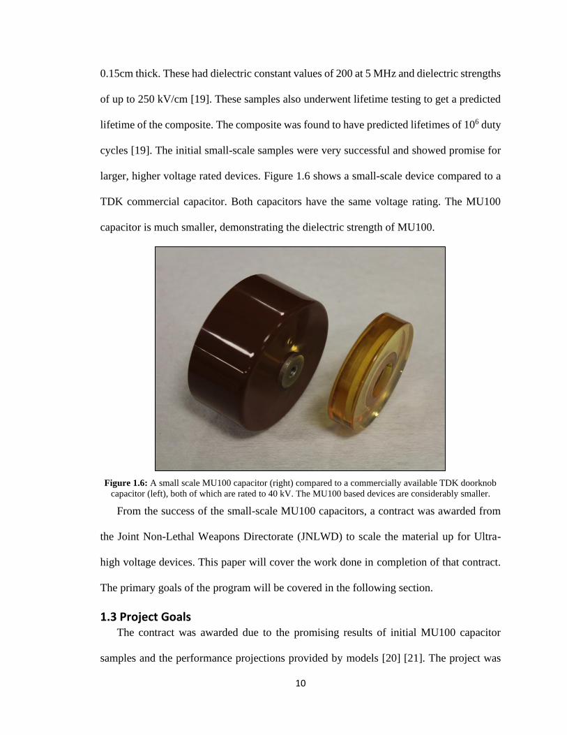
larger, higher voltage rated devices. Figure 1.6 shows a small-scale device compared to a
TDK commercial capacitor. Both capacitors have the same voltage rating. The MU100
capacitor is much smaller, demonstrating the dielectric strength of MU100.
Figure 1.6: A small scale MU100 capacitor (right) compared to a commercially available TDK doorknob
capacitor (left), both of which are rated to 40 kV. The MU100 based devices are considerably smaller.
From the success of the small-scale MU100 capacitors, a contract was awarded from
the Joint Non-Lethal Weapons Directorate (JNLWD) to scale the material up for Ultra-
high voltage devices. This paper will cover the work done in completion of that contract.
The primary goals of the program will be covered in the following section.
1.3 Project Goals The contract was awarded due to the promising results of initial MU100 capacitor
samples and the performance projections provided by models [20] [21]. The project was
Page 22
11
specifically geared toward scaling MU100 up to allow for an ultra-high voltage transfer
capacitor. The final assembly is to be used for pulsed power vehicle stopping systems. The
research goals that enabled the project to be completed are listed below.
1) Continue to develop the high-dielectric constant nanocomposite material, MU100, with
the following focus:
a) Improve dielectric constant of material by 50% at frequencies of 1-15 MHz
b) Maintain dielectric strength in thick substrates (~2 cm thick) to a minimum of
100 kV/cm
c) Increase the material production yield to 90%
2) Characterize the material’s dielectric properties with the following methods:
a) Dielectric spectroscopy
b) High-voltage capacitive discharge
c) Pulsed dielectric strength testing
d) Scanning electron microscopy
e) 3D electrostatic simulations
3) Characterize the thermal dependence of the electrical properties to verify reliability.
4) Design, fabricate, and deliver two long lifetime (>104 pulses) 130 pF, 500 kV
capacitors capable of repeatable performance under pulses with 50-80% voltage
reversal.
a) Test material and devices past minimum requirements.
b) Use test data to reevaluate designs and supply additional, redesigned, test
devices if necessary.
Page 23
12
5) Design, fabricate, and deliver two “Next Generation” capacitors that have the same
electrical performance but allow for a further size reduction of the final device.
a) Scale MU100 to larger diameter substrates.
b) Redesign manufacturing procedures as needed for next-generation design.
Page 24
13
References- Chapter 1
[1] P. Barber, S. Balasubramanian, Y. Anguchamy, S. Gong, A. Wibowo, H. Gao, H.
Ploehn and H.-C. Loye, "Polymer Composite and Nanocomposite Dielectric
Materials for Pulse Power Energy Storage," Materials, pp. 1697-1733, 2009.
[2] M. Rajib, M. Shuvo, H. Karim, D. Delfin, S. Afrin and Y. Lin, "Temperature
Influence on Dielectric Energy Storage of Nanocomposites," Ceramics
Inernational, vol. 41, pp. 1807-1813, 2014.
[3] H. Nalwa, Handbook of Low and High Dielectric Constant Materials and Their
Applications, London: Academic Press, 1999.
[4] J. McPherson, J. Kim, A. Shanware, H. Mogul and J. Rodriguez, "Proposed
universal relationship between dielectric breakdown and dielectric constant,"
International Electron Devices Meeting Digest, 2002.
[5] "Capacitorguide.com," EEtech Media, 11 April 2013. [Online]. Available:
http://www.capacitorguide.com/film-capacitor/. [Accessed 27 June 2019].
[6] G. Atomics, General Atomics Product Brochure, 2019.
[7] L. A. Dissado and J. C. Fothergill, Electrical Degredation and Breakdown in
Polymers, . P. Peregrinus, 1992.
[8] M. H. Sabuni and J. K. Nelson, "The effects of plasticizer on the electric strength of
polystyrene," Journal of Material Science, vol. 14, pp. 2791-2796, 1979.
[9] M. Ieda, "Dielectric Breakdown Process of Polymers," IEEE Transactions on
Electrical Insulation, vol. 15, no. 3, pp. 206-224, 1980.
[10] G. Arlt, D. Hennings and G. de With, "Dielectric properties of fine-grained barium
titanate ceramics," Journal of Applied Physics, vol. 58, pp. 1619-1625, 1985.
[11] TDK, TDK Ultra High Voltage Ceramic Capacitors Brochure, 2017.
[12] K. J. Nelson, Dielectric Polymer Nanocomposites, New York: Springer, 2010.
[13] A. Teverovsky, "Breakdown Voltages in Ceramic Capacitors with Cracks," IEEE
Transactions on Dielectrics and Electrical Insulation, 2012.
[14] C. E. J. Dancer, "Flash Sintering of Ceramic Materials," Materials Research
Express, vol. 3, no. 10, 2016.
[15] R. W. Hertzberg, R. P. Vinci, and J. L. Hertzberg, Deformation and Fracture
Mechanics of Engineering Materials, Wiley, 2013.
Page 25
14
[16] K. O'Connor and R. Curry, "High dielectric constant composites for high power
antennas," in IEEE Pulsed Power Conference, Chicago, 2011.
[17] K. O'Connor and R. Curry, "Recent results in the development of composites for
high energy density capacitors," in IEEE International Power Modulator and High
Voltage Conference, Santa Fe, 2014.
[18] K. O'Connor and R. Curry, "Dielectric studies in the development of high energy
density pulsed power capacitors," in IEEE International Conference on Plasma
Science, San Francisco, 2013.
[19] R. Curry, S. Dickerson, A. Howard, B. Lamb and S. Mounter, "Scaled DC lifetime,
test and evaluation of advanced nanocomposite materials for compact high voltage
capcitorsq," in IEEE 21st International Conference on Pulse Power, Brighton,
2017.
[20] K. O'Connor, "The Development of High Dielectric Constant Composite Materials
and their Application in a Compact High Power Antenna," PhD Dissertation,
University of Missouri, Columbia, 2013.
[21] A. Howard, "Modeling, Characterization and Evaluation of MU100 High-Energy
Density Ceramic NanoDielectric for use in Pulsed Power Applications," M.S.
Thesis, University of Missouri, Columbia, 2016.
Page 26
15
2. THEORY
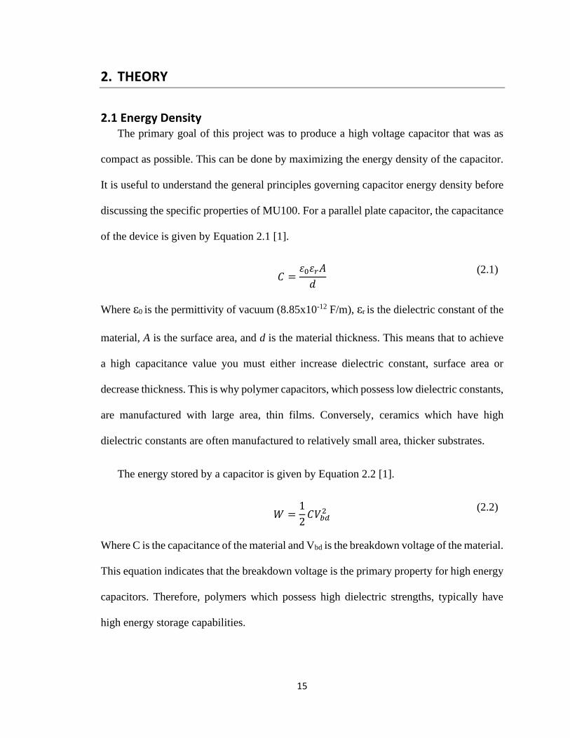
2.1 Energy Density The primary goal of this project was to produce a high voltage capacitor that was as
compact as possible. This can be done by maximizing the energy density of the capacitor.
It is useful to understand the general principles governing capacitor energy density before
discussing the specific properties of MU100. For a parallel plate capacitor, the capacitance
of the device is given by Equation 2.1 [1].
𝐶 =
𝜀0𝜀𝑟𝐴
𝑑
(2.1)
Where ε0 is the permittivity of vacuum (8.85x10⁻¹² F/m), εr is the dielectric constant of the
material, A is the surface area, and d is the material thickness. This means that to achieve
a high capacitance value you must either increase dielectric constant, surface area or
decrease thickness. This is why polymer capacitors, which possess low dielectric constants,
are manufactured with large area, thin films. Conversely, ceramics which have high
dielectric constants are often manufactured to relatively small area, thicker substrates.
The energy stored by a capacitor is given by Equation 2.2 [1].
𝑊 =
1
2𝐶𝑉𝑏𝑑
2
(2.2)
Where C is the capacitance of the material and Vbd is the breakdown voltage of the material.
This equation indicates that the breakdown voltage is the primary property for high energy
capacitors. Therefore, polymers which possess high dielectric strengths, typically have
high energy storage capabilities.
Page 27
16
The energy density of the device is just the energy storage divided by the capacitor
volume as shown in Equation 2.3.
=
𝑊
𝐴𝑑=
1
2𝜀0𝜀𝑟𝐸𝑏𝑑
2 (𝐽
𝑐𝑚3)
(2.3)
Where W is the energy, Ebd is the dielectric strength or breakdown field, and all other
variables are as previously defined. By examining this equation, it is evident that MU100
has unique benefits. If MU100 can successfully combine the high dielectric strength of
polymer with the high dielectric constant of ceramic, very compact ultra-high voltage
capacitors can be achieved.
2.2 Barium Titanate Properties Researchers have been interested in barium titanate as a dielectric material since the
1950’s. This is because barium titanate has many unique properties that give it favorable
electric performance. Barium titanate (BT) belongs to a group of materials known as
perovskites [2]. Perovskites share the same crystalline structure as calcium titanate shown
in Figure 2.1 [3]. Many common oxides take on this structure and have a chemical formula
ABO3, where A and B represent cations and O represents the oxide anion [2]. These crystal
structures can display several symmetries: hexagonal, cubic, orthorhombic, tetragonal or
rhombohedral, all of which have the potential to manifest different physical properties.
Some of these symmetries can produce stable electric dipoles resulting in strong
ferroelectric effects.
Page 28
17
Figure 2.1: A cubic ABO3 perovskite-type unit cell [3].
Barium titanate specifically has four phases: cubic, tetragonal, orthorhombic, and
rhombohedral [4]. The cubic phase exists at temperatures of 120˚C and greater, BT is
tetragonal from 120˚C to 0˚C, the orthorhombic phase is from 0˚C to -70˚C, and
rhombohedral exists for any temperature below -70˚C. When BT is in the cubic phase it
exhibits paraelectric properties [5]. At any phase below the Curie point at 120˚C BT
behaves with ferroelectric properties.
It is the ferroelectric properties of BT that make it of interest for use in capacitors.
Ferroelectricity is the spontaneous alignment of electric dipoles by their mutual interactions
[6]. This phenomenon is made possible by the structure change that occurs in BT when it
changes phases. Figure 2.2 shows the structure change between the paraelectric cubic phase
and the ferroelectric tetragonal phase [7]. When BT transitions into the tetragonal phase
the Ba+2 and Ti+4 cations are displaced relative to the O-2 anion. This displacement
generates a net dipole moment on the structure. When subjected to an electric field, these
Page 29
18
dipole moments will align with respect to the field [8]. The characteristic of spontaneous
alignment is what makes BT an ideal inorganic filler for the polymer matrix.
Figure 2.2: The structure change undergone during the cubic phase to tetragonal phase transition. When
the phase change occurs, the cations displace relative to the anion which generates a dipole moment [7].
In addition to the electrical properties of barium titanate being temperature/phase
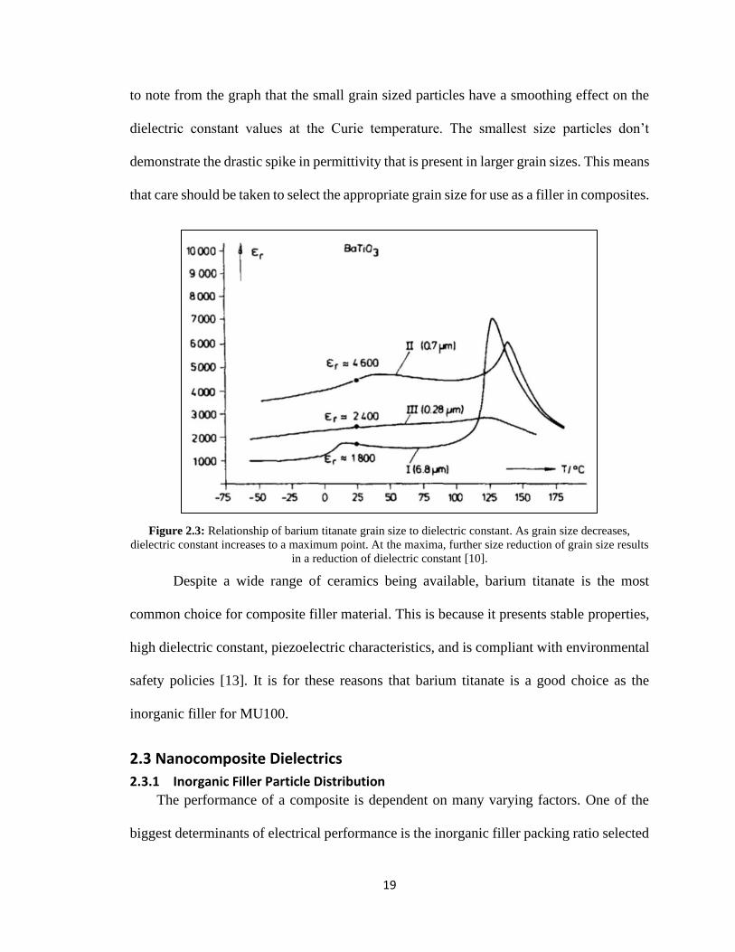
dependent, they are also dependent on grain size [9]. Figure 2.3 shows the relationship of
dielectric constant to grain size of the material [10]. From the graph it is clear that the
dielectric constant increases with decreasing grain size. However, at some grain size there
is a maximum in dielectric constant that is achieved. Beyond this point a further size
reduction of particle grain size results in a decrease of dielectric constant. This is believed
to be a result of the behavior of the individual particle grains. The core of the barium
titanate particle exhibits ferroelectric behavior as previously discussed. However, the outer
grain boundary layer behaves like a “dead-layer” or shows non-ferroelectric characteristics
[11] [12]. As the grain size decreases to the nanometer scale, the outer layer begins to
dominate the characteristics. Theoretically the grain size can be reduced enough where the
ferroelectric properties are no longer recognizable within the material. It is also important
Page 30
19
to note from the graph that the small grain sized particles have a smoothing effect on the
dielectric constant values at the Curie temperature. The smallest size particles don’t
demonstrate the drastic spike in permittivity that is present in larger grain sizes. This means
that care should be taken to select the appropriate grain size for use as a filler in composites.
Figure 2.3: Relationship of barium titanate grain size to dielectric constant. As grain size decreases,
dielectric constant increases to a maximum point. At the maxima, further size reduction of grain size results
in a reduction of dielectric constant [10].
Despite a wide range of ceramics being available, barium titanate is the most
common choice for composite filler material. This is because it presents stable properties,
high dielectric constant, piezoelectric characteristics, and is compliant with environmental
safety policies [13]. It is for these reasons that barium titanate is a good choice as the
inorganic filler for MU100.
2.3 Nanocomposite Dielectrics
2.3.1 Inorganic Filler Particle Distribution
The performance of a composite is dependent on many varying factors. One of the
biggest determinants of electrical performance is the inorganic filler packing ratio selected
Page 31
20
for the composite [14]. The amount of filler used will affect the effective dielectric constant
of the bulk composite. As previously discussed, the particle size selected also has a large
impact on the electrical performance. In order to maximize effective permittivity and
dielectric strength, a packing fraction should be selected to ensure voids are filled [15].
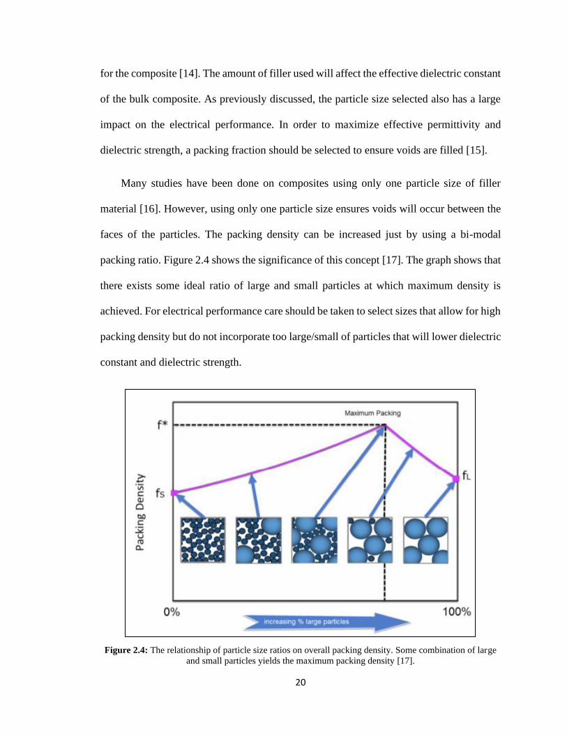
Many studies have been done on composites using only one particle size of filler
material [16]. However, using only one particle size ensures voids will occur between the
faces of the particles. The packing density can be increased just by using a bi-modal
packing ratio. Figure 2.4 shows the significance of this concept [17]. The graph shows that
there exists some ideal ratio of large and small particles at which maximum density is
achieved. For electrical performance care should be taken to select sizes that allow for high
packing density but do not incorporate too large/small of particles that will lower dielectric
constant and dielectric strength.
Figure 2.4: The relationship of particle size ratios on overall packing density. Some combination of large
and small particles yields the maximum packing density [17].
Page 32
21
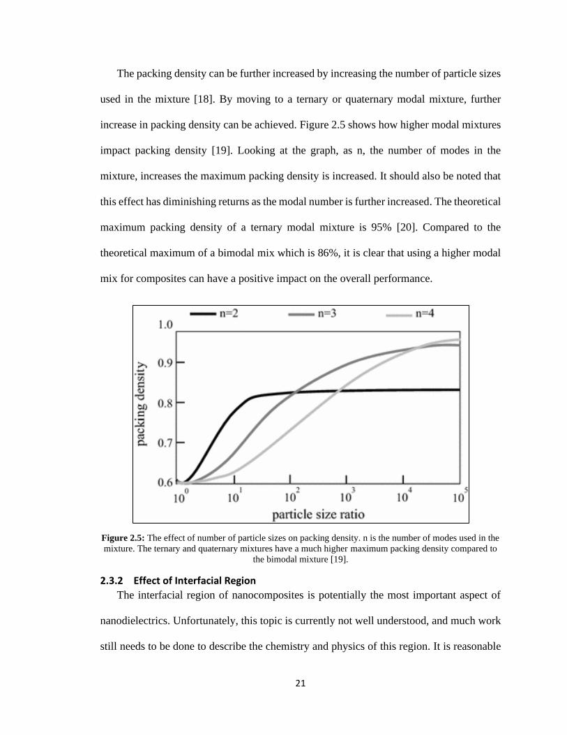
The packing density can be further increased by increasing the number of particle sizes
used in the mixture [18]. By moving to a ternary or quaternary modal mixture, further
increase in packing density can be achieved. Figure 2.5 shows how higher modal mixtures
impact packing density [19]. Looking at the graph, as n, the number of modes in the
mixture, increases the maximum packing density is increased. It should also be noted that
this effect has diminishing returns as the modal number is further increased. The theoretical
maximum packing density of a ternary modal mixture is 95% [20]. Compared to the
theoretical maximum of a bimodal mix which is 86%, it is clear that using a higher modal
mix for composites can have a positive impact on the overall performance.
Figure 2.5: The effect of number of particle sizes on packing density. n is the number of modes used in the
mixture. The ternary and quaternary mixtures have a much higher maximum packing density compared to
the bimodal mixture [19].
2.3.2 Effect of Interfacial Region
The interfacial region of nanocomposites is potentially the most important aspect of
nanodielectrics. Unfortunately, this topic is currently not well understood, and much work
still needs to be done to describe the chemistry and physics of this region. It is reasonable
Page 33
22
to think that a composite would behave with a weighted average of the constituents that
make up the bulk composite. However, nanodielectrics do not perfectly match this model
[16]. This deviation in performance can be attributed to the interfacial region.
The term “interfacial region” is used to describe a specific area within the
nanocomposite. This area begins at the adhesion boundary layer between the inorganic
filler and the polymer. It extends to the point where the polymer matrix resumes its
expected characteristics. Within this region exists characteristics that are distinctly
different from the individual constituents of the composite [21] [22]. The interfacial region
can be considered a separate material from the constituents and is responsible for much of
the favorable properties seen in nanocomposites.
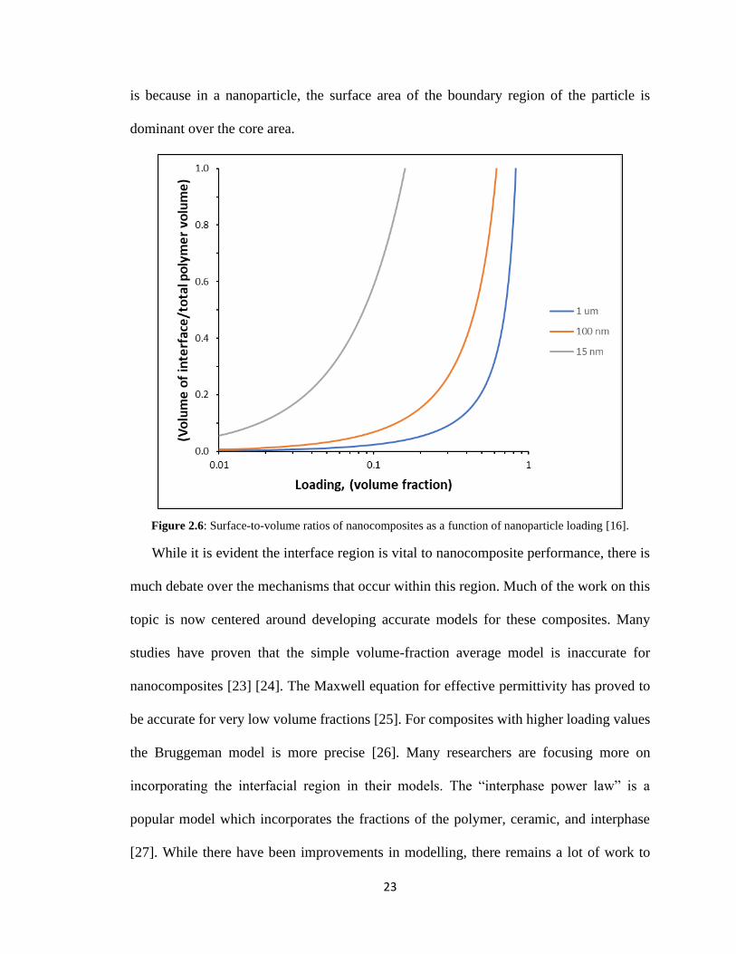
In order to maximize the performance of a nanodielectric, the volume of interfacial
region should be maximized. This is done by utilizing nanoscale particles. The interfacial
region of a microscale particle is insignificant relative to the particle size. However, for
nanoscale particles, the interfacial region is of the same order of magnitude as the particle
itself. This means that nanoscale particles allow for more polymer matrix to be converted
into an interfacial material. This concept is better understood by examining Figure 2.6 [16].
The graph shows the volume of polymer that has been converted to an interface relative to
the total polymer volume as a function of the particle loading. As expected, as the number
of particles within the composite increases, the amount of interfacial region also increases.
What is interesting is that as the particle size decreases, the volume fraction needed to fully
convert the polymer to an interface is significantly decreased. A loading of approximately
16% of 15 nanometer particles is all that is needed to fully convert a polymer matrix. This
Page 34
23
is because in a nanoparticle, the surface area of the boundary region of the particle is
dominant over the core area.
Figure 2.6: Surface-to-volume ratios of nanocomposites as a function of nanoparticle loading [16].
While it is evident the interface region is vital to nanocomposite performance, there is
much debate over the mechanisms that occur within this region. Much of the work on this
topic is now centered around developing accurate models for these composites. Many
studies have proven that the simple volume-fraction average model is inaccurate for
nanocomposites [23] [24]. The Maxwell equation for effective permittivity has proved to
be accurate for very low volume fractions [25]. For composites with higher loading values
the Bruggeman model is more precise [26]. Many researchers are focusing more on
incorporating the interfacial region in their models. The “interphase power law” is a
popular model which incorporates the fractions of the polymer, ceramic, and interphase
[27]. While there have been improvements in modelling, there remains a lot of work to
Page 35
24
allow nanocomposites to be designed from first principles. The leading research in this
topic will continue to focus on understanding the chemistry and structure of the interface
region.
2.4 Electrical Breakdown of Solid Insulators There are many different factors that lead to an electrical breakdown in a solid material.
A breakdown occurs when the insulative material becomes conductive, either momentarily
or permanently [28]. There are many mechanisms that can cause breakdown in a solid,
such as impurities, voids, material degradation, thermal and mechanical stresses, etc. A
breakdown is often a result of many of these mechanisms acting together. Each of these
mechanisms will have a unique statistical probability to cause a breakdown within a
material [29]. Different materials will be more likely to exhibit specific breakdown
mechanisms relative to others. These mechanics can be described as either macroscopic or
microscopic. Macroscopic mechanisms include material defects, voids, and mechanical
stresses. Microscopic mechanisms can be partial charge injection, material degradation,
and electric field inhomogeneity.
2.4.1 Electrical Breakdown of Polymers
Polymers are known for their high dielectric values. One of the reasons for this is
because breakdown in polymers is usually caused by microscopic events. The main causes
for breakdown within polymers are impurities and partial charge injection [16]. Charge
carriers are typically injected into the polymer due to a non-uniform electric field at defects
in the electrode [30]. These charge carriers, once injected, will begin to form conductive
channels under subsequent loading [31]. The end of these conductive channels can be
considered to be needle points which generate extremely high field enhancements within
the material. These field enhancements cause further growth of the channels and will allow
Page 36
25
the channels to branch throughout the material. This process will continue until the
channels reach a point within the material where runaway breakdown occurs [32].
As previously discussed in chapter 1, the ability of charge carriers to freely move will
have a significant impact on how easily conductive channels can form within the material.
Polymers with long free path lengths and weak bonds will allow charge carriers to freely
move throughout the material. It is this charge movement and subsequent collisions that
can lead to electron avalanche causing catastrophic breakdown.
This microscopic process typically occurs over a large time scale. It often takes
thousands of duty cycles to allow for charge carrier accumulation. Typically, there must be
some degradation of the material bond or the electrode to allow for the partial charge
injection process to initiate. This is why polymers are known for their long lifetime
performance.
2.4.2 Electrical Breakdown of Ceramics
Ceramics typically have low dielectric strengths. This is because the predominant
breakdown mechanisms within ceramics can be attributed to macroscopic causes. These
macroscopic mechanisms typically have a higher probability of breakdown due to their
size and associated field enhancements. The biggest macroscopic causes of breakdown are
due to voids, impurities and particle shape/agglomerations [16].
The creation of voids within ceramic material was covered in chapter 1. These voids
will end up behaving like a spark gap when subjected to an electric field. When the field
reaches a certain level the air within the void will breakdown according to Paschen’s law
[33]. If the energy transfer across the void is sufficient, the breakdown will continue
throughout the rest of the bulk material. These voids can be very difficult to detect and are
common within ceramic materials.
Page 37
26
The shape of the particles that form the bulk material also have an impact on its voltage
hold-off capabilities. Many of the models that simulate electric field within a bulk material
assumes that the particles comprising the material have a spherical shape. Unfortunately,
this is rarely true. If the particle has jagged boundaries this will be a cause for field
enhancements. These field enhancements can cause inhomogeneous fields within the
material and high charge buildup at a single location. This charge concentration can
displace electrons within the particle or cause the creation of conductive channels around
the grain boundary [34].
2.4.3 Electrical Breakdown Polymer-Ceramic Composites
The breakdown mechanism for composites are unique. Because the composite
incorporates both polymer and ceramic the breakdown mechanism can be explained as
having contributions from both separate constituents. This means that the macroscopic and
microscopic scale contribute to the overall breakdown process of the composite.
The initiation of breakdown occurs on the microscopic scale. Charge is injected into
the polymer matrix due to degradation or material breakdown. The conducting channels
begin to grow under repeated voltage loads. However, due to the nanofiller component, the
path of the charge carriers is interrupted [35]. This results in a longer path of the conducting
channel which prolongs the life of the material. This process continues until the charge
carriers meet a macroscopic defect in the ceramic material. Once the conductive channel
makes it to this point a catastrophic breakdown is likely. It is for this reason that great care
should be taken when incorporating the inorganic filler to avoid misshapen particles or the
inclusion of voids into the matrix [2].
Page 38
27
It should also be noted that particle size has been found to have a significant impact on
breakdown strength of nanocomposites [36]. Larger macro sized particles are more likely
to generate a larger field enhancement. If conducting channels are near these larger
particles they will grow at a faster rate under the enhanced region.
Page 39
28
References- Chapter 2
[1] R. Fitzpatrick, "Electromagnetism and Optics," University of Texas-Austin, 14 July
2007. Available: http://farside.ph.utexas.edu/teaching/302l/lectures/node41.html.
[Accessed 1 July 2019].
[2] P. Barber, S. Balasubramanian, Y. Anguchamy, S. Gong, A. Wibowo, H. Gao, H.
Ploahn and H. Loye, "Polymer Composite and Nanocomposite Dielectric Materials
for Pulse Power Energy Storage," Materials, vol. 2, pp. 1697-1733, 2009.
[3] K. Momma and F. Izumi, "VESTA 3 for three-dimensional visualization of crystal,
volumetric and morphology data," Journal of Applied Crystallography, vol. 44, pp.
1272-1276, 2011.
[4] G. Kwei, A. Lawson, S. Billinge and S. Cheong, "Structures of the Ferroelectric
Phases of Barium Titanate," Journal of Physical Chemistry, vol. 97, pp. 2368-2377,
1993.
[5] R. Delany and H. Kaiser, "Multiple-Curie-Point Capacitor Dielectrics," IBM Journal
of Research and Development, vol. 11, pp. 511-519, 1967.
[6] S. Roberts, "Dielectric and Piezoelectric Properties of Barium Titanate," Physical
Review Journal, vol. 71, pp. 890-895, 1947.
[7] N. Srivastava and G. Weng, "A Theory of Double Hysteresis for Ferroelectric
Crystals," Journal of Applied Physics, vol. 99, 2006.
[8] Q. Zhang, Properties of Ferroelectric Perovskite Structures, Univeristy of South
Florida: PhD Dissertation, 2012.
[9] K. Kinoshita and A. Yamaji, "Grain-size effects on dielectric properties in barium
titanate ceramics," Journal of Applied Physics, vol. 47, pp. 371-373, 1976.
[10] G. Arlt, D. Hennings and G. de With, "Dielectric properties of fine-grained barium
titanate ceramics," Journal of Applied Physics, vol. 58, pp. 1619-1625, 1985.
[11] L. Curecheriu, M. Buscagila, V. Buscagila, Z. Zhao and L. Mitoseriu, "Grain size
effects on the nonlinear dielectric properties of barium titanate ceramics," Applied
Physics Letter, vol. 97, 2010.
[12] A. Emelyanov, N. Pertsev, S. Hoffmann-Eifert, U. Bottger and R. Waser, "Grain-
Boundary Effect on the Curie-Weiss Law of Ferroelectric Ceramics and
Polycrystalline Thin Films: Calculation by the Method of Effective Medium,"
Journal of Electroceramics, vol. 9, pp. 5-16, 2002.
Page 40
29
[13] M. Vijatovic`, J. Bobic` and B. Stojanovic`, "History and Challenges of Barium
Titanate," Science of Sintering, vol. 40, pp. 235-244, 2008.
[14] M. Rajib, M. Shuvo, H. Karim, D. Delfin, S. Afrin and Y. Lin, "Temperature
Influence on Dielectric Energy Storage of Nanocomposites," Ceramics Inernational,
vol. 41, pp. 1807-1813, 2014.
[15] K. O'Connor, "The Development of High Dielectric Constant Composite Materials
and their Application in a Compact High Power Antenna," PhD Dissertation,
University of Missouri, Columbia, 2013.
[16] K. J. Nelson, Dielectric Polymer Nanocomposites, New York: Springer, 2010.
[17] Malvern Instruments Limited, "Optimizing powder packing behavior by controlling
particle size and shape," Whitepaper, 2016.
[18] C. Furnas, "Grading Aggregates: I-Mathmatical Relations for Beds of Broken Solids
of Maximum Density," Industrial and Engineering Chemistry, vol. 23, pp. 1052-
1058, 1931.
[19] V. Wong and A. Kwan, "A 3-parameter model for packing density prediction of
ternary mixes of spherical particles," Powder Technology, vol. 268, pp. 357-367,
2014.
[20] R. Simpkin, "Derivation of Lichtenecker's Logarithmic Mixture Formula From
Maxwell's Equations," IEEE Transactions on Microwave Theory and Techniques,
vol. 58, no. 3, pp. 545-550, 2010.
[21] J. Manson, "Interfacial effects in composites," Pure & Applied Chemsitry, vol. 57,
no. 11, pp. 1667-1678, 1985.
[22] S. Cheng, B. Carroll, V. Bocharova and A. Sokolov, "Focus: Structure and Dynamics
of the interfacial layer in polymer nanocomposites with attractive interactions,"
Journal of Chemical Physics, vol. 146, 2017.
[23] C. Brosseau, "Modelling and simulation of dielectic heterostructures: A physical
survey from an historical perspective," Journal of Physics D: Applied Physics , vol.
39, pp. 1277-1294, 2006.
[24] Y. Rao, J. Qu, T. Marinis and C. Wong, "A precise numerical prediction of effective
dielectric constant for polymer-ceramic composite based on effective-medium
theory," IEEE Transactions on Components and Packaging Technologies, vol. 23,
no. 4, pp. 680-683, 2000.
Page 41
30
[25] D. Yoon, J. Zhang and B. Lee, "Dielectirc constant and mixing model of barium
titanate composite thick films," Materials Research Bulletin, vol. 38, no. 5, pp. 765-
772, 2003.
[26] Y. Rao and C. Wong, "Material characterization of a high-dielectric constant
polymer-ceramic composite for embedded capacitor for RF applications," Journal of
Applied Polymer Science , vol. 92, pp. 2228-2231, 2004.
[27] M. Todd and F. Shi, "Complex permittivity of composite systems: A comprehensive
interphase approach," IEEE Transactions on Dielectrics and Electrical Insulation,
vol. 12, no. 3, pp. 601-611, 2005.
[28] G. A. Vorob'ev, S. G. Ekhanin and N. S. Nesmelov, "Electrical Breakdown in Solid
Dielectrics," Physics of the Solid State, vol. 47, no. 6, pp. 1083-1087, 2005.
[29] L. A. Dissado, J. C. Fothergill, S. V. Wolfe and R. M. Hill, "Weibull Statistics in
Dielectric Breakdown; Theoretical Basis, Applications and Implications," IEEE
Transactions on Electrical Insulation, Vols. EI-19, no. 3, pp. 227-233, 1984.
[30] V. A. Zakrevski, N. T. Sudar, A. Zappo and Y. A. Dubitsky, "Mechanism of electrical
degradation and breakdown of inulating polymers," Journal of Applied Physics, vol.
93, pp. 2135-2139, 2003.
[31] G. A. Schneider, "A Griffith Type Energy Release Rate Model for Dielectric
Breakdown Under Space Charge Limited Conductivity," Journal of the Mechanics
and Physics of Solids, vol. 61, no. 1, pp. 78-90, 2013.
[32] G. Chen, C. Zhou, S. Li and L. Zhong, "Space charge and its role in electric
breakdown of solid insulation," in 2016 IEEE International Power Modulator and
High Voltage Conference (IPMHVC), San Francisco, 2016.
[33] A. M. Loveless and A. L. Garner, "Universal Gas Breakdown Theory from
Microscale to the Classical Paschen Law," in 2017 IEEE International Conference
on Plasma Science, Atlantic City, 2017.
[34] J. O'Dwyer, The Theory of Electrical Conduction and Breakdown in Solid
Dielectrics, Oxford, UK: Clarendon Press, 1973.
[35] R. Smith, C. Liang, M. Landry, J. Nelson and L. Schadler, "The mechanisms leading
to the useful electrical properties of polymer nanodielectrics," IEEE Transactions on
Dielectrics and Electrical Insulation, vol. 15, no. 1, pp. 187-196, 2008.
[36] T. Lewis, "Nanometric dielectrics," IEEE Transactions on Dielectrics and Electrical
Insulation, vol. 1, no. 5, pp. 812-825, 1994.
Page 42
31
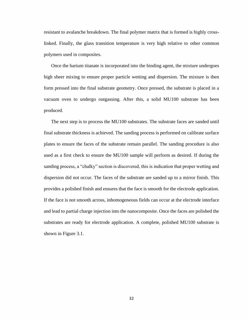
3. MATERIAL PREPARATION
The MU100 is fabricated at the Center for Physical and Power Electronics. The lab
performs nearly every step of the material production. MU100 is comprised of barium
titanate particles with a polymer matrix. The reason MU100 demonstrates many of its
favorable characteristics is because of material selection, processing techniques, and
assembly procedures. Many of these are proprietary in nature. As a result, specific details
on materials used or sample production will not be covered. General material properties
and techniques will be discussed to allow for a basic understanding on how MU100 is
made.
3.1 Barium Titanate Particle Preparation The particle size selection of barium titanate is of great importance to the final capacitor
performance. As discussed in chapter 2, a trimodal mix of particle size can greatly increase
the packing density of the bulk material. The MU100 utilizes a trimodal mix of barium
titanate particles. The specific sizes and loading of each are proprietary. In order to achieve
the desired characteristics for some of the particle sizes it is necessary to produce them in
the laboratory. The particle production process involves many steps but is crucial to the
final performance of MU100.
3.2 MU100 Substrate Production
When the barium titanate particles are prepared they are mixed with the proprietary
polymer binding agent developed at the CPPE. The specific composition of the binder will
not be covered but it has several general characteristics that contribute to the favorable
performance of MU100. The binder is highly compatible with barium titanate, forming
covalent bonds with the inorganic filler. The binder has a short free length which makes it
Page 43
32
resistant to avalanche breakdown. The final polymer matrix that is formed is highly cross-
linked. Finally, the glass transition temperature is very high relative to other common
polymers used in composites.
Once the barium titanate is incorporated into the binding agent, the mixture undergoes
high sheer mixing to ensure proper particle wetting and dispersion. The mixture is then
form pressed into the final substrate geometry. Once pressed, the substrate is placed in a
vacuum oven to undergo outgassing. After this, a solid MU100 substrate has been
produced.
The next step is to process the MU100 substrates. The substrate faces are sanded until
final substrate thickness is achieved. The sanding process is performed on calibrate surface
plates to ensure the faces of the substrate remain parallel. The sanding procedure is also
used as a first check to ensure the MU100 sample will perform as desired. If during the
sanding process, a “chalky” section is discovered, this is indication that proper wetting and
dispersion did not occur. The faces of the substrate are sanded up to a mirror finish. This
provides a polished finish and ensures that the face is smooth for the electrode application.
If the face is not smooth across, inhomogeneous fields can occur at the electrode interface
and lead to partial charge injection into the nanocomposite. Once the faces are polished the
substrates are ready for electrode application. A complete, polished MU100 substrate is
shown in Figure 3.1.
Page 44
33
Figure 3.1: Complete, sanded and polished MU100 substrate.
3.3 Electrode Deposition
The electrode deposition process is vital to the performance of MU100. The electrode
must be uniform across the face and have a sufficient bond to the dielectric material.
Without these, when voltage is applied to the capacitor, nonuniform fields will build until
the substrate breaks down. Many different materials and application procedures have been
tested on MU100 samples [1]. The most effective electrode has been found to be a silver
electrode applied using sputter deposition.
The sputter coating process is performed using a Cressington 108 Auto shown in Figure
3.2. During the sputtering process a high energy DC field is used to accelerate ions toward
a target [2]. These ions bombard the target and as a result, atoms of the target material are
ejected. These ejected atoms impact the MU100 material in the chamber. This process is
important because the ejected atoms have enough energy to partially embed into the
substrate. This ensures that a strong bond is made between the electrode and dielectric
material. This is critical to ensure the electrode does not peel off during assembly and
subsequent handling. The sputtering process also allows for a fairly uniform electrode to
be deposited. For smaller diameter substrates the silver sputtered electrode is sufficient.
Page 45
34
For larger diameter substrates the silver sputter electrode is used as a seed layer for copper
electroplating.
Figure 3.2: Cressington 108 Auto sputter coater in operation. The machine is used to silver sputter coat
MU100.
After the sputtering process, the substrates are electroplated if needed. The difference
between the sputtered and electroplated electrodes will be discussed in depth later in this
work. To electroplate, the sides of the substrates are covered with adhesive copper tape to
ensure every face of the substrate is conductive. The electroplating procedure is performed
as shown using the constructed plating tank shown in Figure 3.3 per the Caswell Plating
Manual [3]. A high-quality piece of copper is placed in an electrolytic solution to act as the
anode. The substrate is placed in the solution and wired to act as the cathode. A direct
current is then applied to anode causing the copper to ionize and dissolve into the solution.
The copper ions then plate onto the ground potential cathode. This process leaves a layer
of copper that is bonded to the silver seed layer. The plating is continued until a layer of
Page 46
35
copper approximately 50 µm thick is achieved. The substrates are then removed from the
plating bath and allowed to fully dry. At this point the sample is complete and ready to be
tested and used as a capacitor.
Figure 3.3: Plating tank built to copper electroplate MU100 substrates.
Page 47
36
References- Chapter 3
[1] S. Dickerson, R. Curry, S. Mounter and L. Brown, "Compact Very High Voltage
Capacitor Development Based on Advanced Machinable, NanoDielectric Materials,"
in IEEE International Power Modulator and High Voltage Conference, Jackson, WY,
2018.
[2] J.-C. Pivin, "An overview of ion sputtering physics and practical implications,"
Journal of Material Science, vol. 18, no. 5, pp. 1267-1290, 1983.
[3] Caswell Inc., Caswell Plating Manual Version 10, Caswell Inc., 2012.
Page 48
37
4. TEST METHODS AND EQUIPMENT
Material characterization is extremely valuable when producing a new material. In
order to understand the impact process modifications have on material performance,
standard testing procedures must be established. Sometimes tests are common and one can
use existing testing standards to attain desired measurements. For other tests, industry
standards may not exist, and a custom test stand and protocol must be produced. The
following sections will cover all test methods and equipment used to characterize the
MU100 substrates.
4.1 Dielectric Constant Measurements The first measurement performed on the completed samples was to record the dielectric
constant value. This was done by using the Agilent 4285A Precision LCR meter [1]. Figure
4.1 shows the LCR meter and special shielded capacitance probe. The meter operates over
a range of 75 kHz to 30 MHz. The measurements taken for MU100 were recorded for a
frequency of 5 MHz to match the expected field application of the material. The
capacitance values being recorded for MU100 were in the picofarad range. As a result, it
was vital to recalibrate the meter before each measurement. When measuring properties
that are that small, minor changes in air conditions can impact the overall capacitance
reading. The high precision of this meter was needed to get accurate measurements of the
MU100 samples. Once capacitance was recorded the dielectric constant was calculated
using Equation 2.1.
Page 49
38
Figure 4.1: The Agilent 4285A Precision LCR meter. This meter was used to take capacitance
measurements on the MU100 disks.
4.2 PA-80 Dielectric Strength Testing To measure the dielectric strength of the MU100 substrates, destructive over-volt
testing had to be performed. This testing was done according to ASTM 3755-14 [2]. The
samples are placed under a high voltage DC pulse. The samples are monitored during the
tests to watch for signs that they have broken down and are no longer able to hold off the
applied voltage. The applied voltage is incrementally increased until breakdown is
achieved. The breakdown voltage divided by the substrate thickness gives the average
dielectric strength of the substrate. This process is repeated until a sufficient number of
data points is gathered to characterize the mean dielectric strength of MU100. As the
substrate thickness of the material is increased, it follows that the applied voltage needed
for breakdown also increases. For thinner samples, the PA-80 test stand was used to carry
out the testing.
The PA-80 test stand is designed to provide a fast risetime, high voltage pulse for the
thin MU100 samples. Figure 4.2 shows the overall test stand. The primary component of
the test stand is a commercial L-3, PA-80 pulse generator. The pulse generator allowed for
Page 50
39
a maximum voltage of 80 kV with a risetime of 100 ns. A full list of specifications from
the PA-80 pulse generator can be seen in Table 4.1 [3]. The pulse generator is charged by
an 80 kV power supply. Diagnostics are taken using an oscilloscope protected by a Faraday
cage.
Figure 4.2: Complete PA-80 test stand for dielectric strength testing. L-3 PA-80 Pulse Generator and
monitoring circuit (Right), test stand power supply (Center), Oscilloscope in Faraday cage (Left).
Table 4.1: Summarization of the performance specifications of the PA-80-Mk2 pulse generator used to
evaluate thin substrates under a high-voltage pulsed condition. [3]
Charge Voltage 5 - 80 kV
Stored Energy (at 80 kV) 240 Joules
Output Voltage with a 50 Ω
Matched Load
80 kV
Output Voltage with an
Open Circuit
∼160 kV
Output Rise Time (10-90 %) ∼100 ns
Accessory Gas Required SF6 at 100 psig
Page 51
40
The voltage that is applied to the test sample is measured using two NorthStar PVM
series high voltage probes [4]. The probes and the diagnostic circuit are shown in Figure
4.3. The probes are placed on either side of the substrate being evaluated. The max
difference between these two probes correlates to the maximum voltage applied to the
substrate. When the difference goes to zero a break down has occurred. A typical waveform
from the PA-80 is shown in Figure 4.4.
Figure 4.3: High voltage probes used to measure voltage across test capacitor.
Figure 4.4: Typical PA-80 waveform. The traces from both voltage probes can be seen.
Page 52
41
4.3 The 250 kV Test Stand As the MU100 capacitors were scaled up from thin substrates their voltage hold-off
capabilities increased. The full-scale substrates had a voltage rating of over 240 kV.
Because of this high breakdown value, the PA-80 test stand was no longer sufficient to
perform dielectric strength testing. A new custom test stand had to be designed and built
to allow the larger samples to be tested. Design of the new stand was done by the guidance
of standard ASTM 3755-14 [2].
The new test stand would need to provide a DC unipolar pulse at a voltage up to 250
kV to ensure the scaled-up samples could be overvolted. The test stand was designed to
reach these ultra-high voltages through the method of CLC resonant charging. This method
is useful because it allows a higher output voltage on the test capacitor than what was used
for the charge voltage.
This phenomenon is made possible by the way the capacitor-inductor-capacitor (CLC)
circuit behaves when energized. This can easily be understood by looking at Equation 4.1
which shows the maximum voltage applied to the test capacitor [5]. As the load capacitance
is decreased, the overall voltage seen on the test capacitor is increased. This is explained
by Equation 2.2 [6]. The charge capacitors are charged to a certain energy level before
discharge. When the switch is closed the energy is transferred from the charged capacitors
to the load capacitor under test. Since the load capacitance is significantly smaller, the
voltage on the load device will increase to allow for the same energy level to be achieved.
It should be noted that the theoretical maximum voltage that can be achieved is twice the
charge voltage. However, energy is not perfectly transferred to the load capacitor. Losses
through the inductor, resistor, and conductor connections decrease the voltage increase that
is actually measured. Through calibrating the test stand it was found that the custom 250
Page 53
42
kV test stand had a voltage increase of 1.7-1.8 times the initial charge voltage, depending
on the value of the load capacitance.
𝑉𝐶,𝑙𝑜𝑎𝑑 =
2𝑉𝑜
1 +𝐶𝑙𝑜𝑎𝑑
𝐶𝑏𝑎𝑛𝑘
(4.1)
A circuit diagram of the custom 250 kV test stand is shown in Figure 4.5. The test stand
uses a 150 kV power supply to charge the storage capacitors. The storage capacitors used
are Maxwell S series (P/N 31165) [7]. Three of these capacitors were placed in series to
form a capacitor bank with a voltage rating of 300 kV and a capacitance of 13.33 nF. A
spark gap is used as the switch for the test stand. The spark gap is filled with SF6 gas. When
the capacitor bank is fully charge, pressure is reduced inside the spark gap until the gas
breaks down and the capacitor bank is discharged. The series inductor of the network is a
copper wound inductor with an inductance of 5.5 µH. There also is a series resistance to
damp the ringing discharge. The test stand uses two different voltage dividers, one made
of capacitors and one of resistors, to aid in diagnostics. The voltage dividers step the
voltage down to allow two Tektronix high-voltage probes (P6015A) to measure the voltage
at a pick off point [8]. This is passed to a 500 MHz oscilloscope shielded by a Faraday
cage. A picture of the 250 kV CLC circuit is shown in Figure 4.6.
Figure 4.5: Circuit diagram of the 250 kV Test Stand.
Page 54
43
Figure 4.6: Assembled 250 kV test stand. Circuitry is immersed in dielectric oil bath to prevent flash over.
The completed circuit performs as designed. The maximum output voltage applied to
a normal load capacitor is 265 kV. This is the highest the stand can be charged to without
risking damage to the power supply. The pulse risetime of the test stand is 110 ns. A typical
waveform from the 250 kV test stand is shown in Figure 4.7. The test stand is also capable
of repetitive pulse discharge at a frequency of 1 pulse per second. This allows for full scale
lifetime testing to be performed on the samples. With this test stand, characterization of the
scaled up MU100 substrate’s dielectric strength was made possible.
Page 55
44
Figure 4.7: A typical waveform from the 250 kV test stand.
4.4 Thermal Characterization Methods It is of great interest to know how a material’s properties change with temperature. The
MU100 prototype is expected to see a varying range of temperature during field
application. It was decided to look at key properties to ensure the device would perform to
specifications over a varying temperature range. The change in dielectric constant with
temperature was the first property that was evaluated. The coefficient of thermal expansion
for MU100 was then determined. Finally, the dielectric strength versus temperature was
investigated. The following sections will discuss the test methods and equipment used to
gather this data.
4.4.1 Dielectric Constant vs. Temperature
In order to take the dielectric constant measurements at varying temperatures a custom
test stand was designed and built. The test stand and test procedures were designed using
Page 56
45
the guidance of test standard ASTM D2149-13 [9]. The targeted temperature range of the
test stand was from -30˚C to 125 ˚C. This allows for the Curie temperature and all phase
transition temperatures to be examined.
The test stand consisted of a heating chamber, refrigeration chamber, and the Agilent
4285A LCR meter. The heating/cooling rate had to be controlled to not exceed a rate of
2.5 ˚C/min. To control the heating/cooling rate, the stand was fitted with a Raspberry Pi 3
single board computer to control the temperature to the heating and cooling chambers.
A picture of the dielectric constant temperature test stand is shown in Figure 4.8. The
thermal cycling chamber was constructed using plywood with aluminum sheet metal
facing. The interior of the chamber was lined with a layer of aluminum foil faced, foam
insulation. The chamber was fitted with two, 250 W heat lamps. These heat lamps provide
the necessary heating source to reach the maximum desired temperature. A stand was built
to secure both leads of the LCR meter to the capacitor while heating and cooling. The
temperature was controlled by a Raspberry Pi 3 program. The controller took
measurements of the temperature chamber at a frequency of 1Hz. The power source for the
heat lamps was connected to a relay that was controlled by the Raspberry Pi. The controller
would open/close the relays as needed to allow for the desired temperature input to be
reached.
The thermal cycling of the samples at low temperatures was achieved by using a
commercial miniature freezer. This was selected as the best option due to the cost and time
of building a separate refrigerant system. A cutout was made in the side insulation to allow
the LCR cables and temperature probe to pass through. The temperature was monitored
using a Type K temperature probe. Steps also had to be taken to ensure the internal
Page 57
46
temperature of the test sample was being measured and not just the surface temperature.
To make this measurement, a MU100 sample was bored out to allow a temperature probe
to be inserted at the center of the sample piece. The sample pieces are shown in Figure 4.9.
Figure 4.8: Test equipment used to characterize MU100's change in dielectric constant with temperature.
The heating chamber with Raspberry Pi controller (left), the LCR meter and temperature meter (center), the
cooling chamber (right).
Figure 4.9: Samples used to monitor MU100 internal temperature. Samples were bored out and fitted with
thermocouple. A bare MU100 substrate or a potted substrate could be used to match the test sample
configuration.
Page 58
47
4.4.2 Coefficient of Thermal Expansion
The next property that was analyzed was the coefficient of thermal expansion (CTE)
for MU100. This property is important to characterize to determine how the composite will
expand or contract when heated and cooled. A buildup of mechanical stresses can
negatively impact dielectric strength of a material, or even cause fractures.
To measure the CTE, steps were followed from standard ASTM E831-19 [10]. The
temperature range targeted was from -40˚C to 100˚C to cover the expected operational
range of the device. The heating/cooling of samples was achieved by using the thermal
chambers discussed in the previous section. Samples were placed unrestrained in the
chamber to allow for unimpeded elongation/contraction in the axial direction. Once
thermal equilibrium was achieved, sample lengths were measured using a high precision
micrometer. Each sample was marked to ensure measurements were taken from the same
location at each temperature, this accounted for any minor variation in disk thickness across
the face. The temperature of the samples was monitored using the same Type K
temperature probe and MU100 sample as described in the previous section.
4.4.3 Dielectric Strength Versus Temperature
The MU100 property of greatest interest is how dependent the dielectric strength is on
material temperature. The final capacitor assembly is expected to see a wide range of
temperatures during field use and is expected to withstand full voltage throughout all of it.
The process of obtaining dielectric strength at room temperature is well established. The
most applicable standard is ASTM D3755-14 [2]. However, the process of testing the
dielectric strength across large temperature ranges is not well established. No active
standard exists which outlines the test equipment and procedure needed. An inactive test
standard ASTM D3151-88(1998) was used as a baseline and then was expanded upon to
Page 59
48
yield the end procedure and setup [11]. This section will cover the design process and
manufacturing of the 250 kV temperature test stand.
The design process of the thermal test stand began with identifying the requirements
necessary to complete characterization of the dielectric strength temperature dependency.
A summary of the test stand requirements is given below:
Thermal Test Stand Requirements
• Provide a high voltage DC pulse up to 250 kV
• Heat/cool substrate to temperatures from -40˚C to 100˚C and maintain temperature
for extended periods
• Regulate temperature to allow for a desired heat exchange rate
• Actively monitor temperature of MU100
• Easily change out test samples
The test stand had to be capable of providing up to 250 kV to a test sample to allow for
the thickness of 1.8cm substrates to be evaluated. The stand needed to be able to reach
temperatures between -40˚C to 100˚C and maintain that temperature for long periods of
time. This allows for MU100 to be evaluated for all of the expected field application
temperatures and to ensure that thermal equilibrium is reached throughout the substrate
before voltage is applied. The temperature chamber needed to have a control process that
would allow the heat exchange rate to be regulated. This prevents the test sample from
being exposed to thermal shock. The temperature of the substrate had to be monitored
throughout the entire testing process. It was also important to make changing the test
samples as easy as possible to allow for more tests to be conducted per day.
There were also several concerns to be factored into the design philosophy of the test
stand. These concerns are summarized below.
Page 60
49
Thermal Test Stand Design Concerns
• Mitigation of safety hazards
• Dielectric oil contamination
• Material selection
• Overall cost
Great care had to be taken to identify all safety concerns before ever using the test
stand. Proper grounding procedures on all components had to be used to eliminate the
concern of electric shock. Care had to be taken to ensure the dielectric oil would not be
contaminated with other heat exchanger mediums. The properties of the dielectric oil bath
had to be accounted for to mitigate the chance of an oil fire. All materials selected had to
be capable of operating within the temperature range, electrically non-conductive, and
compatible with the dielectric oil. Additionally, the cost of each subcomponent had to be
minimized to ensure the overall budget was met.
It was decided to use the existing 250 kV test stand as the base component of the
thermal test stand. This allowed for the most efficient completion of the required test stand.
The remainder of the design would then need to be carried out to allow for easy integration
into the existing pulse circuit. The conceptual design is shown in Figure 4.10. Shell Diala
AX transformer oil was used as the heat exchanger fluid [12]. This decision allowed us to
eliminate concerns of contaminating the Diala AX oil bath that the 250 kV circuit was
sitting in. The heat exchanger medium also had to be able to electrically insulate around
the MU100 sample, and the Diala oil was ideal for this. A reservoir would be needed to
hold the oil while being heated and cooled. A pump would then circulate the oil, once at
temperature, to the test chamber. The test chamber would hold the test sample, allowing
the voltage to be applied and the oil to circulate through, transferring heat. A
heating/cooling system schematic of the design is shown in Figure 4.11.
Page 61
50
Figure 4.10: 3-D model of the 250 kV temperature test stand design. A pump would be used to transfer
heated/cooled oil to a sealed test chamber.
Figure 4.11: A schematic of the heating and cooling system for the temperature test stand.
Page 62
51
The reservoir for the system was the first component that was fabricated. The reservoir
had to be liquid tight and withstand the temperatures. It also had to easily accommodate
the heating and cooling systems. After conducting a trade study, it was found that the only
economically viable option to obtain a refrigerant system was to purchase a commercially
available freezer. Sole condensing units capable of very low temperatures can be
purchased, but at ten times the price of the commercial freezer unit. A SO-LOW CH40-5
chest freezer was purchased [13]. This freezer was selected because it had a sheet metal
interior that would withstand heating. The seams of the interior were sealed using a liquid
welded adhesive. The heating of the oil was done using two, 1500W submersible heating
elements. These were placed within the oil reservoir. The heating elements were wired
using separate breakers to allow the maximum current draw through them when energized.
A motor with a propeller attached was mounted between the heating elements to circulate
oil. This increased the heat exchange rate within the reservoir. The freezer and heating
system are shown in Figure 4.12.
Figure 4.12: The CH40-5 freezer used as the cooling mechanism and oil reservoir (Left). Two 1500W
submersible heating elements used to heat the oil (Right).
Page 63
52
The next step was finding a proper pumping mechanism to circulate the oil. Several
factors were considered when selecting the pump. First, all the wetted parts of the pump
had to be compatible with the oil. Many pumps used seals or rotor materials that would
dissolve over time in the transformer oil. The pump also had to be able to withstand the
full temperature range. Again, the seals were a concern when it came to both extremes of
the temperature range. The overall system pressure required was very low. It was calculated
that pump would need to produce a minimum head pressure of 20 ft. This accounted for
the oil properties and all connection losses within the system. The pump would also have
to be able to provide 4 ft of suction lift. A relatively high flow rate was also desired to aid
in heat transfer within the test chamber.
The largest issue with the pump selection was that it would have to circulate a very
wide range of viscosity values for the oil. The pour point of the Diala oil is -47˚C which
means that the oil would be extremely viscous at the lower temperatures [12]. The oil was
tested per ASTM D1343-95 to determine the viscosity of the oil throughout the temperature
range [14]. It was found that the pump would have to be able to circulate oil between 2.3cSt
to 100cSt. This meant that a gear pump was the only viable option to pump the oil at -40˚C.
A heavy-duty Haight 6UR Gear Pump shown in Figure 4.13 was selected [15]. The
pump is constructed from all cast iron parts and has a single Viton seal. This ensures that
the pump can withstand the full temperature range and is compatible with the oil. It has a
flow rate of 6 gpm and can easily produce the pressures needed to circulate the oil. The
gears make oil circulation possible at the lower temperatures where viscosity is high. A
special PTFE tubing was also purchased, to connect all the components, that could
withstand the temperatures and was chemically resistant. A water coalescing filter was
Page 64
53
connected to the pump to account for any water pulled out of the air when oil is cooled to
sub-freezing temperatures.
Figure 4.13: Heavy duty gear pump used to circulate oil from reservoir to test chamber.
The test chamber was the system component that would integrate into the 250 kV
circuit and hold the MU100 test sample. The biggest challenge with the test chamber design
was material selection. The material had to be electrically non-conductive, have an
operational temperature within the targeted temperature range, be compatible with the oil,
be easy machinable to allow manufacture, and be affordable. This list of requirements
severely limited the materials that were viable. Acrylic was selected as the test chamber
material. The internal forces on the chamber were calculated and found to be well within
the capabilities of acrylic. The 100˚C applied temperature would mean some slight
softening of the material. However, verification tests were performed on pieces of Acrylic
at that temperature and it was determined the functionality of the chamber would not be
compromised at 100˚C. The melting point of Acrylic is 160˚C.
Page 65
54
A cast Acrylic tube was purchased. The ends of the tube were tapped to allow for bolts
to fast end caps into place. The endcaps were designed to seal the chamber with internal
O-rings [16]. The high voltage endcap was fitted with pressure fit electrodes to hold the
MU100 capacitor during testing. The high voltage endcap as manufactured is shown in
Figure 4.14. The high voltage end cap was connected to the ground end cap using a braided
cable. The grounded endcap contained a fixture to allow a center drilled piece of MU100
to be mounted to act as a temperature monitor. A sealed wire pass through was attached to
the end cap to allow a temperature probe to be inserted into the drilled MU100 sample.
This allowed for material core temperature to be monitored during operation. A bare
MU100 disk and an encapsulated disk were used as references depending on if the sample
being tested was encapsulated or not. Both end caps were fitted with PTFE tubing to allow
the oil to be pumped through the test chamber. The chamber was also mounted at an angle
inside the 250 kV test stand tank to allow entrapped air to escape. This mitigated concern
of flash over in the oil during testing. Figure 4.15 shows the final assembled test chamber.
Figure 4.14: High voltage endcap. End cap has a pressure fit electrode stand to secure the capacitor and
provide the test voltage.
Page 66
55
Figure 4.15: Completed test chamber. The high voltage end cap is to the right, the ground end cap to the left.
Control of the complete system was achieved using a Raspberry Pi 3 board running a
control program. Inputs were taken from temperature probes located in the oil reservoir
and the test chamber. Relays were actuated sending power to the freezer, heaters, or pump
as needed based on the desired test chamber temperature. The pump and heaters were also
fitted with manual override switches as an added safety layer. As the oil was heated/cooled
in the reservoir, it was circulated to the test chamber to allow the MU100 temperature to
be gradually changed and thus avoiding thermal shock. A photograph of the control set up
for the test stand is shown in Figure 4.16.
Page 67
56
Figure 4.16: Test stand control set up. A Raspberry Pi program was used to actuate the relays shown on the
right. This controlled the power to the heating, cooling, and pumping elements. This also served as a safety
against overheating the oil.
The last concern was that the oil would not maintain its dielectric properties as needed
across the temperature range. To verify the oil performance a Hipotronics OC60D oil
dielectric tester was used [17]. Samples of oil were heated and cooled to the extremes of
the expected test stand conditions and then tested. Breakdown testing confirmed that the
dielectric strength of the oil was not affected by the temperatures.
Once fabricated, all components were connected and integrated into the existing 250
kV test stand. The final assembly of the test stand is shown in Figure 4.17. The assembled
thermal test stand functioned as designed. The oil was able to be heated/cooled to every
temperature within the required range. The pump successfully circulated the oil at a
sufficient flow rate. The test chamber successfully sealed and allowed the oil to be pumped
back to the reservoir. The test chamber also allowed a 250 kV pulse to be applied to a
capacitor without adding significant noise to the output waveform. The control system
worked to autonomously modulate the temperature as needed and acted as a safeguard
Page 68
57
against heating the oil to high. The test stand was successfully used to characterize the
dielectric strength dependence of MU100.
Figure 4.17: Completed 250 kV temperature test stand. The heating/cooling chamber and pump above tank
(top). The test chamber integrated into the 250 kV test stand (bottom).
Page 69
58
References- Chapter 4
[1] Agilent Inc., 4285A Precision LCR Meter, Technical Data Sheet, 2008.
[2] ASTM International, ASTM D3755-14, Standard Test Method for Dielectric
Breakdown Voltage and Dielectric Strength of Solid Electrical Insulating Materials
Under Direct-Voltage Stress, West Conshohocken, PA: www.ASTM.org, 2014.
[3] L-3 Communications, PA-80 and PA-100 Trigger Generators, Technical Data Sheet,
2008.
[4] North Star High Voltage, PVM Series Portable High Voltage Probes to 100 kV DC,
Technical Data Sheet, 2011.
[5] Ness Engineering, "Ness Engineering Inc.," Ness Engineering Inc, October 2014.
[Online]. Available: http://www.nessengr.com/technical-data/resonant-charging/.
[Accessed 23 June 2019].
[6] R. Fitzpatrick, "Electromagnetism and Optics," University of Texas - Austin, 14 July
2007.Available:http://farside.ph.utexas.edu/teaching/302l/lectures/node41.html.
[Accessed 1 July 2019].
[7] General Atomics and Affiliated Companies, Series S/SS High Voltage 1 pps
Capacitors, Technical Data Sheet, 1994.
[8] Tektronix Inc., P6015A 1000X High Voltage Probe, P6015A Manual, 2006.
[9] ASTM International, Standard Test Method for Permittivity (Dielectric Constant)
And Dissipation Factor Of Solid Ceramic Dielectrics At Frequencies To 10 MHz And
Temperatures To 500°C, West Conshohocken, PA: www.ASTM.org, 2013.
[10] ASTM International, Standard Test Method for Linear Thermal Expansion of Solid
Materials by Thermomechanical Analysis, West Conshohocken, PA:
www.ASTM.org, 2019.
[11] ASTM International, ASTM D3151-88(1998), Standard Test Method for Thermal
Failure of Solid Electrical Insulating Materials Under Electric Stress (Withdrawn
2007), West Conshohocken, PA: www.ASTM.org, 1998.
[12] Shell Inc., SHELL DIALA OILS A & AX Electrical Insulating Oil, Technical Data
Sheet, 2014.
[13] SO-LOW Environmental Equipment CO., Inc., SO-LOW Chest Style Freezer Model
C40-5, Cincinnati, Ohio: Technical Data Sheet, 2018.
Page 70
59
[14] ASTM International, ASTM D1343-95(2011) Standard Test Method for Viscosity of
Cellulose Derivatives by Ball-Drop Method, West Conshohocken, PA: ASTM
International, 2011.
[15] Haight Pumps, 6EU Operating Manual, Evansville, WI: Haight Pumps, 2012.
[16] Parker Hannifin, Parker O-ring Handbook, Cleveland, OH: Parker, 2018.
[17] Hipotronics, OC60D Manual, Brewster, NY: Hipotronics, 2009.
Page 71
60
5. THE 1ST GENERATION PROTOTYPE PRODUCTION
The goal of the project was to develop a final device capable of operating under a
voltage load of 500 kV. To achieve this, the MU100 substrates needed to be scaled up in
size to allow for higher voltage ratings. Both the diameter and thickness of the substrates
were increased. Once scaled up, work was focused on the design and fabrication of a
prototype that met the required specifications. The work done on the first phase of this
project will be briefly covered in this chapter. A fully detailed discussion of the work done
during this phase of research can be found in Dickerson’s work [1].
5.1 Material Scaling The original MU100 substrates produced to test the feasibility of using the material for
capacitors were very thin with diameters of 2.54 cm. These original samples are shown in
Figure 5.1. These substrates showed impressive dielectric strength performance, often
reaching values greater than 250 kV/cm [2]. The dielectric constant had a typical value of
200. The maximum voltage rating for these thin substrates was approximately 40 kV [3].
In order to satisfy the project requirements, the substrates would need to be significantly
increased in size to give them a larger voltage rating.
Figure 5.1: Initial 2.54 cm diameter substrates. These initial small-scale samples had high dielectric
strengths, often >250 kV/cm.
As the material volume was increased, a decrease in both dielectric strength and
dielectric constant was observed. Part of the decrease in performance was attributed to
Page 72
61
simple volume theory which states that a larger volume corresponds to a higher probability
of defects within a bulk material [4]. The decrease in dielectric strength followed the
relationship given in Equation 1.1 [5]. However, the material volume increase only
accounted for a portion of the decreased performance.
The way in which the substrates were manufactured had to be modified to account for
the new volume. Changes were made to ensure that proper particle wetting was being
achieved. This ensured that all particle faces were being incorporated into the polymer
matrix. Changes were also made to the packing fractions to achieve higher densities of the
final substrate. Improvements were also made to the particle processing procedures to
achieve smoother, more uniform barium titanate particles. These changes, when
incorporated, yielded a much improved MU100 material. Scanning electron microscope
imaging was used throughout this process to track the changes made to the material. The
images taken of MU100 before and after the production improvements are shown in Figure
5.2. The before image shows jagged, irregular micro scale particles with a sparse
surrounding of nano scale particles. The mixing improvements led to a higher packing
density as seen in the after image. The micro scale particles are surrounded by nanoscale
particles which increases the material’s capabilities. The micro scale particles are also less
jagged due to particle production improvements. This means that they produce less of a
field enhancement when under an electric field. These improvements led to consistent,
reliable material performance.
Page 73
62
Figure 5.2: SEM images of MU100 before and after production improvements. Before (left), After (right).
The improvements led to a higher packing density of particles and micro scale particles that were more
uniform with smoother edges.
5.2 Field Shaping Electrode With the material production refined, focus was turned to other aspects of the capacitor.
As the material was being tested a consistent breakdown failure was noted. The MU100
samples were consistently failing due to edge breakdown. Edge breakdown occurs when
the field enhancements due to the electrode/dielectric interface, often called the triple point,
are high enough to cause the material in the area to fail. This often results in the material
failing along the outer edge and allowing an arc to pass to the other electrode. An example
of edge breakdown is shown in Figure 5.3. CST Studio Suite, an electromagnetic field
simulation software, was used to better understand the fields on the capacitor. Figure 5.4
shows the results of the simulation. It can be seen how the flat electrode produces a high
field enhancement region at the edge of the dielectric material. The average field used in
this simulation was 125 kV/cm. The maximum field within the MU100 at this interfacial
region was found to be 620 kV/cm. This gives a field enhancement factor of 4.96. It was
this field enhancement that produced the edge breakdowns on the capacitors.
Page 74
63
Figure 5.3: Early MU100 capacitor demonstrating an edge breakdown failure.
Figure 5.4: The CST simulation of electric fields on MU100 substrate. The full substrate is shown on the
left. A zoomed in view of the electrode interface is shown on the right.
Once the breakdown mechanism was identified, solutions were explored to lower the
field enhancement at the triple point. It was decided to design a corona ring electrode for
the capacitors. The electrode would act to hide the triple point and to push the high fields
away from the dielectric material and into the high dielectric potting. CST simulations were
run to optimize the geometry of the field shaping electrode. Several iterations of electrodes
were tested before a final design was achieved. The CST simulations of the final design
are shown in Figure 5.5. With the field shaping electrodes applied the peak field in the
MU100 was 138.75 kV/cm. This means the field enhancement factor is only 1.11, a near
80% reduction from the flat electrode design.
Page 75
64
Figure 5.5: The CST simulation showing the resulting electric fields with field shaping electrodes applied
to the capacitor. The full capacitor is shown on the left. A zoomed in view of the triple point is shown on
the right. The field shaping electrode successfully pushes the field enhancement region away from the
dielectric material and into the high strength potting.
With the final design complete, the field shaping electrodes were tested with MU100
samples. Figure 5.6 shows a cross section from dielectric strength testing. The field shaping
electrode successfully eliminated premature failure due to edge breakdown. The
breakdown failure shown is through the bulk of the material.
Figure 5.6: Cross section of dielectric strength testing with final field shaping electrode applied. With the
addition of the field shaper, the breakdown occurred through the bulk of the material.
5.3 Capacitor Design and Production The MU100 production improvements, coupled with the field shaping electrode
allowed for the capacitors to be significantly scaled up in size. The scaling progression of
the material is shown in Figure 5.7. The material was successfully scaled from thin, 2.54
cm diameter substrates to 2 cm thick, 3.4 cm diameter substrates. The field shaping
electrodes allowed further improvements to be made in dielectric strength performance.
Page 76
65
The final scaled up substrates had an average dielectric strength of 120 kV/cm. The average
dielectric constant was 160. With stable, scaled up substrates, work was started on
producing the capacitor prototype.
Figure 5.7: The material scaling progression of MU100. The initial thin, 2.54 cm diameter samples (left),
the scaled up 3.4 cm diameter samples (middle), final half scale prototype with field shapers (right).
The final capacitor requirements were to provide a 130 pF capacitor capable of
withstanding 500 kV with 50%-80% voltage reversal. The device would also have to be
capable of long lifetime performance, 105-106 shots. The final design was centered around
properly derating the capacitor to allow for each specification. To extend the lifetime of
the capacitor it is preferable to operate the device at 80% of its maximum voltage rating
[6]. To account for the voltage reversal that will be seen during field application a further
derating of 35% was given. When both deratings are applied to the average dielectric
strength of 120 kV/cm, an operational dielectric strength of 66 kV/cm is achieved. This
operational dielectric strength is what was used during the design process to ensure the
final device had the margins needed to operate successfully. Less conservative deratings
can be used to further reduce the device size, but with an increased risk of device failure.
For the final capacitor to have a voltage rating of 500 kV with an operational dielectric
strength of 66 kV/cm, the total material thickness needed is approximately 8 cm.
Four, 2 cm thick substrates were stacked in series to form an 8 cm thick submodule.
The substrates were brazed together with a eutectic solder. The assembled submodules had
Page 77
66
an average capacitance of 15.5 pF. In order to fulfill the final 130pF capacitance
requirement, 9 submodules were placed in parallel. The assembly progression for the
device is shown in Figure 5.8. The final device has dimensions of a 15 cm cube and weighs
12 lbs. Two of these prototypes were made and tested.
Figure 5.8: Assembly progression of the capacitor prototype. 2 cm thick MU100 substrate (left), 500 kV
15.5 pF submodule (middle), 500 kV, 130 pF final capacitor (right).
5.4 Capacitor Performance The final prototypes were shipped to NSWC Dahlgren for testing. The capacitors were
tested using a Marx bank generator capable of pulse charging a matched capacitive load to
nearly 600 kV and ringing it at a specific frequency with 55%-60% voltage reversal. The
rise time of the system was approximately 50 ns, with a pulse width on the order of a
microsecond. The devices were tested at 500 kV with 60% reversal. A typical waveform
from the testing is shown in Figure 5.9. Both capacitors were subjected to over 10,000 full
voltage pulses. Throughout the entirety of the testing no breakdown or sign of device
degradation occurred. Both delivered devices successfully met the project requirements.
Page 78
67
Figure 5.9: Typical waveform from full voltage capacitor testing. The device was subjected to a minimum
of 500 kV with a voltage reversal of approximately 60%.
Single submodules were also shipped to be tested under full voltage conditions. These
submodules were subjected to over voltage testing to baseline the maximum capabilities of
the assembly. Due to the small load capacitance of the single submodules the Marx
generator was able to supply over a megavolt to the submodules [7]. Figure 5.10 shows a
typical waveform from the submodule overvoltage testing. These submodules were placed
under a 1.1 MV load with 10% voltage reversal [7]. The ring frequency of the test circuit
was monitored during testing to track the degradation or failure of the capacitor. The Marx
generator discharges into an RLC circuit. The ringing frequency of this circuit is dictated
by the capacitance value of the test capacitor. If the ringing frequency changes it indicates
that the capacitor has either significantly degraded or failed. Figure 5.11 shows the
recorded ringing frequency collected during one of the submodule overvoltage tests. At
approximately 170 seconds into testing the ringing frequency changed indicating device
failure. This test time corresponded to just over 1000 pulses. Both submodules tested had
Page 79
68
lifetimes of 1,000 shots at 1.1 MV. The MU100 capacitors performed better than expected
during the testing. The requirements were met and exceeded. The first-generation
prototypes were a success.
Figure 5.10: Typical waveform from single submodule overvoltage testing. Submodules were subjected to
approximately 1.1 MV with 10% reversal.
Figure 5.11: Ring frequency of test circuit vs. testing time or number of shots.
Page 80
69
References- Chapter 5
[1] S. A. Dickerson, Advanced NanoDielectric Material Development and Scaling for use
in Compact Ultra-High Voltage Capacitor Prototypes, M. S. Thesis, University of
Missouri, Columbia, Mo, 2019.
[2] R. Curry, S. Dickerson, A. Howard, B. Lamb and S. Mounter, "Scaled DC lifetime,
test and evaluation of advanced nanocomposite materials for compact high voltage
capcitorsq," in IEEE 21st International Conference on Pulse Power, Brighton, 2017.
[3] A. Howard, "Modeling, Characterization and Evaluation of MU100 High-Energy
Density Ceramic NanoDielectric for use in Pulsed Power Applications," M.S. Thesis,
University of Missouri, Columbia, 2016.
[4] R. W. Hertzberg, R. P. Vinci and J. L. Hertzberg, Deformation and Fracture Mechanics
of Engineering Materials, Wiley, 2013.
[5] J. McPherson, J. Kim, A. Shanware, H. Mogul and J. Rodriguez, "Proposed universal
relationship between dielectric breakdown and dielectric constant," International
Electron Devices Meeting Digest, 2002.
[6] S. Dickerson, R. Curry, S. Mounter and L. Brown, "Compact Very High Voltage
Capacitor Development Based on Advanced Machinable, NanoDielectric Materials,"
in IEEE International Power Modulator and High Voltage Conference, Jackson, WY,
2018.
[7] S. Dickerson, L. Brown, R. Curry, and S. Mounter, " Ultra-High Voltage
NanoDielectrCapacitor Development, and Testing for Compact Pulsed Power," in
IEEE Pulsed Power and Plasma Science Conference, Orlando, FL, 2019.
Page 81
70
6. THERMAL CHARACTERIZATION
The thermal characterization of the MU100 substrates was possible as soon as the
scaled-up samples showed consistent, reliable performance at room temperature. The
MU100 substrates and final capacitors had been subjected to a vast number of different
tests. All these tests however were performed at standard ambient temperature conditions.
How the material would perform under varying temperatures was unknown. To better
understand the material’s thermal response three properties of chief interest were analyzed:
dielectric constant, coefficient of thermal expansion, and dielectric strength. All testing
was performed using the equipment outlined in chapter 4. The results of the testing and
implications will be fully discussed in the following sections.
6.1 Dielectric Constant vs. Temperature The dielectric constant of MU100 was measured between -30˚C to 125 C. Capacitance
measurements versus temperature were collected for multiple samples of MU100. Multiple
samples were subjected to the heating and cooling cycle to reduce background noise in the
baseline in order to characterize the dielectric material’s response. Multiple, different test
sweeps were run for each substrate to provide a good average. Data was collected through
the temperature range by sweeping through both hot to cold and cold to hot. It is necessary
to run the tests in both directions to account for any hysteresis effects the material may
present based on the direction of temperature swing. Additionally, humidity effects were
lessened by sampling through the temperature range in both directions.
The test specimen was brought to either the high or low end of the test range and
allowed to soak for approximately an hour to ensure thermal equilibrium of the sample was
achieved. The specimen was then either heated or cooled at a rate of 2°C/min per ASTM
Page 82
71
D2149-13 [1]. Capacitance measurements were taken every 5°C. At temperatures near
known state transitions of barium titanate, the measurement interval was decreased to every
2.5°C to allow for sufficient resolution to capture the maximums at these points.
Figure 6.1 shows a typical result from the dielectric constant testing. The graph shows
several things that are interesting for characterizing MU100. First, the dielectric constant
is reasonably stable across a wide temperature range. The MU100 shows a local maximum
in dielectric constant when it transitions between the tetragonal and orthorhombic phases
between 0°C to 5°C. This matches the behavior seen with pure sintered barium titanate [2].
The MU100 has an overall maximum value at the Curie temperature of 120°C. However,
the drastic increase common in pure barium titanate is not seen in MU100. This is believed
to be due to the nonpolar behavior of the binding agent used and the highly cross-linked
polymer matrix that is formed within MU100 [3]. The dampening effect can also be
attributed to the composite nature of MU100. The particles in MU100 are all incorporated
into a polymer matrix, as opposed to being fused together as in pure sintered barium
titanate. This means that the individual structure change of a particle has less of an impact
on the whole material in the composite. Whereas, in the sintered material, a structure
change of a single grain will directly impact the adjacent grain structures. This coupled
with the multimodal mixture of MU100 eliminates the drastic value changes at phase
transition points [4]. The values of MU100’s dielectric constant are lower than pure
sintered barium titanate. This decrease is attributed to the different particle sizes used
within the composite which increase the voltage hold-off of MU100. The smaller grain
sizes of the particles coupled with the polymer binder decrease the overall dielectric
constant values [5].
Page 83
72
Figure 6.1: Typical MU100 Dielectric Constant vs. Temperature curve. Dielectric constant is stable across
all temperatures. The phase change of the tetragonal structure can clearly be seen at approximately 0°C.
Samples of other materials were analyzed using the same test methods and were
compared with MU100. A disk of 99% pure barium titanate sintered at 1375°C was
analyzed along with a commercially available ultra-high voltage TDK ceramic capacitor.
The TDK UHV-9A capacitor was selected because it has similar performance values as
MU100 [6]. Figure 6.2 shows the test results of the three different materials. The percent
difference of capacitance relative to 25°C was taken for each test. The three different
materials vary widely from each other. Barium titanate exists in three phases for the test
temperature range: orthorhombic below 0ºC, tetragonal at 0ºC to 120ºC, and cubic above
120ºC. Barium titanate is stable throughout the tetragonal phase. It then drops drastically
at 0°C when it transitions to an orthorhombic structure and rises sharply at 120°C when it
transitions to a cubic phase. The commercial capacitor also varies drastically from the
baseline room temperature capacitance. The commercial product exhibits a maximum
Page 84
73
percent difference of 38% occurring at 105°C. The MU100 exhibits very favorable thermal
stability qualities by changing little with temperature. The tetragonal phase stability of
barium titanate is preserved in MU100 while not exhibiting the drastic changes at extreme
temperatures. MU100 has a maximum percent difference of 9.8% occurring at 130°C. This
result is significant when comparing it to other readily available commercial capacitors.
The particle sizes selected, coupled with the polymer binder, produce a dielectric material
that does not manifest a strong temperature dependence, even at extreme temperatures.
This ensures that capacitor performance will remain relatively constant across all expected
field application temperatures.
Figure 6.2: Percent difference of capacitance of different samples, relative to capacitance at 25°C. MU100
varies a max of 9.8%. Both BaTio3 and the commercial capacitor vary much more drastically.
6.2 Coefficient of Thermal Expansion The next property analyzed was the coefficient of thermal expansion. This mechanical
property is important to understand for the final assembly of the device. How MU100
changes dimensionally with temperature is important because it is part of a multi-
Page 85
74
component assembly. Understanding how the material changes with temperatures provides
insight on potential CTE mismatch issues relative to the electrodes used and the
encapsulant surrounding the assembly.
The temperature range used during the test was -20°C to 100°C. Test specimens were
allowed to soak in the chamber until thermal equilibrium was achieved. After thermal
equilibrium, length measurements were taken axially for each cylinder per ASTM E831-
19 [7]. Measurements were taken in 10°C increments. Cylinders of 99% pure sintered
barium titanate and high dielectric strength epoxy were manufactured to similar sizes as
the MU100 disks and were tested for comparison. The epoxy analyzed is the epoxy that is
used to encapsulate the final assembly of a MU100 capacitor. The epoxy is comprised of
Hexion 815C resin and Hexion 3140 curing agent. Figure 6.3 shows the three different
materials that were analyzed.
Figure 6.3: Three different materials analyzed during thermal expansion tests. High dielectric strength
epoxy (left), MU100 (center), BaTiO3 (right).
All three materials were analyzed multiple times to achieve a stable baseline. Figure
6.4 shows the typical results for all three materials. It is immediately evident how little
MU100 changes with temperature when compared to the other two materials. The epoxy
sample shows the largest dimensional change with temperature. The coefficient of thermal
expansion for the epoxy was calculated to range from 7-9.1 PPM/°C depending on the
temperature point being analyzed. Barium titanate shows a slightly improved stability over
the epoxy with the calculated coefficient of thermal expansion to range from 6-8.4 PPM/°C
Page 86
75
depending on temperature. The results for barium titanate match well with previously
published results [8] [9]. The MU100 exhibits minimal length change for all temperatures
within the test range. The maximum coefficient of thermal expansion recorded was 1.5
PPM/°C. It is believed that the reduced thermal expansion of MU100 compared to barium
titanate is due to the nanoscale particles and the multimodal mixture used in the composite
[10]. The very high glass transition temperature of the polymer binder also allows for the
stable behavior. These results show that MU100 provides a mechanically stable base for
capacitor assemblies under thermal loading and avoids the negative electrical effects
associated with high thermal strain values [11].
Figure 6.4: Relative change of sample length vs. temperature. MU100 shows minor dimension change
across a wide range of temperatures.
6.3 Dielectric Strength vs. Temperature Characterizing the dependence of dielectric strength to temperature was the property
of greatest interest relative to the project goals. The capacitor prototypes will be expected
Page 87
76
to perform under ultra-high voltage at a varying range of temperatures. Determining
MU100’s voltage holdoff at all these temperatures was vital to ensure confidence in the
final capacitor assemblies.
Destructive breakdown voltage testing was performed on MU100 samples for
temperatures between -40˚C to 100˚C. This temperature range was selected because it
encompassed all foreseeable temperatures the final capacitor would be subjected to during
field application. It was decided to select five temperatures of interest and test multiple
samples at each point to obtain a good characterization of behavior across the entire
temperature range. The temperatures tested were -40˚C, 0˚C, 25˚C, 60˚C, and 100˚C. The
samples being tested were slowly brought to the desired test temperature to mitigate the
thermal strain in the sample. The samples were allowed to soak at the test temperature to
ensure thermal equilibrium throughout the test sample. Once thermal equilibrium was
achieved, the test samples were subjected to progressive voltage testing until dielectric
breakdown occurred. The breakdown voltage of the sample was recorded and divided by
the sample thickness to give the dielectric strength.
The result from the breakdown testing is shown in Figure 6.5. Eight to ten samples of
MU100 were tested at each temperature of interest. The graph shows the average from each
data set for all the test temperatures. The MU100 shows virtually no change in dielectric
strength for the entirety of the temperature range. The error bars of the graph show the
standard deviation for the data sets at each temperature. The spread of values in each data
set is relatively small. MU100 demonstrated consistent dielectric performance between
samples and across temperature. The largest data spread occurs at the highest temperature
which is expected.
Page 88
77
Figure 6.5: Average breakdown field vs temperature for MU100. The error bars show the standard
deviation for the data sets at each temperature. The dielectric strength of MU100 shows virtually no change
across the test temperatures.
A common method of expressing dielectric strength data for solids is the Weibull
distribution [12]. This distribution is preferable because it is suited for small data sets [13].
Good approximations are able to be made with only a few data points. The Weibull plots
are often used to estimate device reliability versus voltage or duty cycles. The two-
parameter Weibull distribution cumulative density function is given by Equation 6.1.
𝐹(𝑥) = 1 − exp (−
𝑥
𝛼)
𝛽
(6.1)
Where:
x Is the breakdown voltage of an individual substrate.
F(x) Is the probability of failure at a voltage less than or equal to x.
α Is the scale parameter.
β Is the shape parameter.
The Weibull analysis was performed in accordance with standard IEC 62539 [14]. Each
data set from the different test temperatures was analyzed individually. The breakdown
field values from a data set were ordered from smallest to largest and then assigned a rank
Page 89
78
based on the ordering. Median ranks were assigned to each breakdown value as probability
percentages. The correlation between the breakdown fields and median ranks was then
calculated to check that the Weibull distribution was a good fit for the data. All data sets
showed a good correlation to the Weibull distribution. The values in the data sets were then
assigned weightings based on the total sample size and the scale and shape parameter
estimates were calculated. Finally, the 90% confidence interval was calculated for each
data set.
The Weibull plot produced from the analyses of the data taken at standard ambient
temperature is shown in Figure 6.6. The plots from the other temperature data sets are very
similar to the ambient temperature plot and will not be shown for brevity. The dashed line
in the figure shows the resulting Weibull function. The true data points from the testing are
shown as the points. The solid, black lines are the upper and lower limits for the 90%
confidence interval of the Weibull function.
Figure 6.6: Typical Weibull probability plot of percent probability of breakdown vs. breakdown field. The
dashed line shows the Weibull function, the test data is shown with the points, the 90% confidence interval
is the area between the solid, black lines.
Page 90
79
The resulting shape and scale parameters that were fit to each temperature data set are
shown in Table 6.1. The values are significant for many reasons. First, the scale factor is
extremely consistent regardless of temperature. The scale factor corresponds to the point
on the Weibull plot where there is a 63.2% probability of breakdown. The consistency of
this value across temperature is another measure of how little MU100’s dielectric strength
is dependent on the temperature test range. The shape factors are relatively high for all the
data sets. This shows that the range of breakdown field is not very large. The higher the
shape factor value the smaller the spread of data points. The averages of the calculated
parameters were taken for all the test temperatures. The average values can be used in
Equation 6.1 to get an estimate of failure probability for an applied electric field if the exact
operating temperature is not known.
Table 6.1: Weibull parameters for all temperature data sets. The bottom row shows the averaged values to
give a general approximation for the entire temperature range.
Temperature (˚C) α, Scale Factor β, Shape Factor
100 118.262 24.849
60 117.404 44.786
25 118.889 42.091
0 118.795 42.672
-40 119.292 38.824
AVERAGED α AVERAGED β
-40˚C to 100˚C 118.528 38.644
It was theorized that the high dielectric epoxy used to encapsulate the MU100 could
impact the dielectric strength at different temperatures. Due to the CTE mismatch it was
thought the encapsulant might delaminate from the dielectric material. This separation
would allow for a potential air gap down the side of the dielectric material. The internal
forces induced by the compression from the epoxy were also a concern. To determine if
this could occur, tests were conducted on samples of bare MU100 and samples of
encapsulated MU100. Figure 6.7 shows an example of both test samples. The Field shaping
Page 91
80
electrodes were applied to every sample to ensure breakdowns were a result of bulk
material failure and not due to the electrode interface.
Figure 6.8 shows the comparison between potted and unpotted samples at all test
temperatures. Several potted and unpotted samples were tested at each temperature of
interest to get a baseline. The results show no distinguishable difference in dielectric
strength between potted and unpotted samples at any of the investigated temperatures.
After testing it was noted that the encapsulant had remained adhered to the dielectric
material regardless of the heating/cooling cycle. This also confirms that any internal
stresses induced in the MU100 are negligible in terms of overall performance.
Figure 6.7: Typical MU100 samples used during dielectric strength vs temperature characterization. Fully
potted capacitor (left), unpotted capacitor (right).
Figure 6.8: Breakdown field across temperature for potted and unpotted samples. There is no
distinguishable difference in dielectric strength performance between potted and unpotted samples.
Page 92
81
References- Chapter 6
[1] ASTM International, ASTM D2149-13, Standard Test Method for Permittivity
(Dielectric Constant) And Dissipation Factor Of Solid Ceramic Dielectrics At
Frequencies To 10 MHz And Temperatures To 500°C, West Conshohocken, PA:
www.ASTM.org, 2013.
[2] R. A. Delaney and H. D. Kaiser, "Multiple-Curie-Point Capacitor Dielectrics," IBM
Journal of Research and Development, vol. 11, no. 5, pp. 511-519, 1967.
[3] R. Popielarz, C. K. Chiang, R. Nozaki and J. Obrzut, "Dielectric Properties of
Polymer/Ferroelectric Ceramic Composites from 100 Hz to 10 GHz,"
Macromolecules, vol. 34, pp. 5910-5915, 2001.
[4] G. Arlt, D. Hennings and G. de With, "Dielectric properties of fine-grained barium
titanate ceramics," Journal of Applied Physics, vol. 58, pp. 1619-1625, 1985.
[5] K. Kinoshita and A. Yamaji, "Grain-size effects on dielectric properties in barium
titanate ceramics," Journal of Applied Physics, vol. 47, pp. 371-373, 1976.
[6] TDK, TDK Ultra High Voltage Ceramic Capacitors Brochure, 2017.
[7] ASTM International, Standard Test Method for Linear Thermal Expansion of Solid
Materials by Thermomechanical Analysis, West Conshohocken, PA:
www.ASTM.org, 2019.
[8] G. Shirane and A. Takeda, "Transition Energy and Volume Change at Three
Transitions in Barium Titanate," Journal of the Physical Society of Japan, vol. 7, no.
1, pp. 1-4, 1952.
[9] Y. He, "Heat capacity, thermal conductivity, and thermal expansion of barium
titanate-based ceramics," Thermochimica Acta, vol. 419, pp. 135-141, 2004.
[10] L. M. Sullivan and C. M. Lukehart, "Zirconium Tungstate (ZrW2O8)/Polyimide
Nanocomposites Exhibiting Reduced Coefficient of Thermal Expansion," Chemistry
of Materials, vol. 17, no. 8, pp. 2136-2141, 2005.
[11] T. Taylor, P. Hansen, B. Acikel, N. Pervez, R. York, S. Streiffer and J. Speck,
"Impact of thermal strain on the dielectric constant of sputtered barium strontium
titanate thin films," Applied Physics Letters, vol. 80, pp. 1978-1980, 1978.
[12] R. Abernathy, The New Weibull Handbook, Robert B. Abernathy, 2000.
Page 93
82
[13] P. Barber, S. Balasubramanian, Y. Anguchamy, S. Gong, A. Wibowo, H. Gao, H.
Ploahn and H. Loye, "Polymer Composite and Nanocomposite Dielectric Materials
for Pulse Power Energy Storage," Materials, vol. 2, pp. 1697-1733, 2009.
[14] IEC, Guide for the statistical analysis of electrical insulation breakdown data, IEC,
2007.
Page 94
83
7. NEXT GENERATION CAPACITOR MATERIAL SCALING
The delivery of the first generation 500 kV capacitor was a success. The MU100, 3.4
cm diameter substrates performed better than originally expected. As a result, the project
was extended to develop a second-generation 500 kV capacitor using MU100. The second-
generation device has the same performance requirements as the first but was also required
to provide an even smaller, final form factor. This chapter covers the material scaling
process used to meet the requirements given.
7.1 Initial Scaling In order to further reduce the final size of the capacitor the MU100 substrates had to be
modified. It was decided to scale the substrate diameter from 3.4 cm to 6.35 cm. The
dielectric strength is dependent on the volume of the material. Therefore, if the first- and
second-generation substrates have the same volume, they should also have the same
dielectric strength values. From Equation 2.1, by increasing the diameter of the substrate
and decreasing the thickness, the resulting capacitance is dramatically increased. This rise
in capacitance while maintaining dielectric strength allows for the final assembly to be
produced with a smaller number of sub-modules.
The initial scaling attempts to the larger diameter substrates were not successful.
Despite theory stating that dielectric strength should be the same, the average dielectric
strength was approximately 40% less than the 3.4 cm substrates. Regardless of the poor
dielectric strength, the 6.35 cm substrates did show favorable capacitance values which
showed promise for the new substrate design. The poor dielectric performance indicated
that substrate production process improvements would be needed to accommodate for the
new geometry.
Page 95
84
7.2 Production Improvements The production processes used on the 3.4 cm substrates did not allow for perfect scaling
to the 6.35 cm substrates. Several changes were made to the proprietary mixing process to
accommodate the wider pressing form. Specifics of the changes will not be discussed in
depth. These changes were implemented and resulted in a dielectric strength performance
increase of approximately 17%. The substrates also demonstrated consistent breakdown
values with the implemented improvements. With the material performance stabilized,
focus was shifted to other potential causes of the low dielectric strength of the larger
substrates.
7.3 Electrode Improvements With the production improvements employed, the 6.35 cm substrates were
demonstrating consistent dielectric performance but still had dielectric strength values that
were well under the anticipated values. It was theorized that the low dielectric strength was
not due to the material but the electrode. The initial 6.35 cm substrates were tested with
silver sputtered electrodes as was done with the 3.4 cm substrates.
To test the electrode performance, 6.35 cm substrates were tested with just a silver
sputtered electrode and a copper electroplated electrode. The two test cases are shown in
Figure 7.1. The samples were electroplated as described in section 3.3. Multiple test
samples of each type were subjected to breakdown voltage testing until a good baseline of
performance was established per ASTM D3755-14 [1].
Page 96
85
Figure 7.1: Two different electrodes tested on the 6.35 cm substrate. Silver sputtered electrode (left), silver
sputtered seed layer with copper electroplated electrode (right).
The results of the electrode testing are shown in Figure 7.1. For comparison, results
from breakdown testing of the 3.4 cm substrate was included. The mean values of each
data set are denoted with an X. The brackets mark the maximum and minimum values in
each data set. The substrates with a copper plated electrode perform significantly better
than the 6.35 cm samples with sputtered electrodes. The copper plating provides an
approximately 38% dielectric strength increase relative to the 6.35 cm sputtered electrode
baseline. The mean dielectric strength of the copper plated 6.35 cm substrate is 117 kV/cm.
This is virtually the same as the average dielectric strength of the 3.4 cm samples.
Figure 7.2: Dielectric strength values of different MU100 substrate configurations. Mean values are
marked with an x for each data set. Brackets indicate the max and min values of each data set.
Page 97
86
The differences in performance due to the electrode application method are due to the
surface area of the second-generation substrates. The 3.4 cm substrate dielectric strength
was independent of electrode application type. Many samples were tested with both
sputtered and electroplated faces. No difference in dielectric performance was observed in
the 3.4 cm samples. It is believed that the silver sputter deposition technique is not
sufficient to adequately cover the increased surface area of the 6.35 cm samples. It is well
documented that inconsistent electrode surfaces result in decreased voltage hold-off
capability [2]. Varying electrode densities and roughness will result in an inhomogeneous
field across the face of the substrate when subjected to an electric field. This inconsistent
field will result in charge accumulation at the peak fields and initiate the breakdown
process. The electroplating technique is better suited to large surface areas and provides a
uniform, thick electrode across the entire face.
The processing improvements coupled with the electrode improvements resulted in a
successfully scaled 6.35 cm MU100 substrate. Figure 7.3 shows a comparison between the
3.4 cm diameter and 6.35 cm diameter substrates. Both substrates have the same volume
of material. The 6.35 cm substrate has an average capacitance of 850 pF, dielectric constant
of 170, and an average dielectric strength of 117 kV/cm.
Figure 7.3: MU100 substrate comparison. 3.4 cm x 2 cm substrate (Left), 6.35 cm x 0.6 cm substrate
(Right). Both substrates have the same volume of material.
Page 98
87
References- Chapter 7
[1] ASTM International, ASTM D3755-14, Standard Test Method for Dielectric
Breakdown Voltage and Dielectric Strength of Solid Electrical Insulating Materials
Under Direct-Voltage Stress, West Conshohocken, PA: www.ASTM.org, 2014.
[2] K. J. Nelson, Dielectric Polymer Nanocomposites, New York: Springer, 2010.
Page 99
88
8. NEXT GENERATION CAPACITOR DESIGN & ASSEMBLY
With the 6.35 cm substrates performing well, work began on designing the new
capacitor assembly. The new capacitor would also need to be designed to withstand a 500
kV pulse with 50%-80% voltage reversal for lifetimes of 104 shots. The final capacitance
of the device must be a minimum of 130 pF. The following sections will discuss the
adjustments made to the design and assembly process in order to meet the project
requirements.
8.1 Capacitor Design To finalize the capacitor design the performance of the larger MU100 substrates was
analyzed with the final requirements and the operating safety margin desired. The final
design balanced the margin of the final device and overall device size. The first step was
to determine the total thickness of material needed. The first-generation capacitors were
overdesigned in that they had a much higher voltage holdoff than was intended. It was
decided to pursue a more aggressive second-generation design to allow for a maximum
size reduction of the overall device. The voltage derating for long life performance was
decreased from 20%, given on the first device, to 15%. The derating given to compensate
for the voltage reversal was decreased from 35% to 20%. This yields a net 35% voltage
derating for the capacitor. This gives a maximum rated voltage of 772 kV. The larger
substrates have an average dielectric strength of 117 kV/cm. To achieve the voltage rating
a material thickness of approximately 6.6 cm is required. The 6.35cm substrates had a
typical thickness of 0.6 cm. Thus, eleven substrates stacked in series was required to
achieve the needed voltage rating.
Page 100
89
The average capacitance of a 6.35 cm X 0.6 cm substrate is 850 pF. For eleven
substrates in series, the resulting capacitance of a sub-module is approximately 75 pF. To
achieve the required minimum capacitance of 130 pF, two submodules were placed in
series. This gives the final device a capacitance of 150 pF. The final device is 15% over
the minimum required capacitance. The conceptual design of the full assembly is shown in
Figure 8.1.
Figure 8.1: The 3-D conceptual assembly of the second-generation 500 kV capacitor. Comprised of two
stacks in parallel, stacks consist of 11, 6.35cm disks in series. Full assembly with encapsulant (Left).
Assembly without encapsulant to allow for a better view of dielectric material (Right).
8.2 6.35cm Field Shaping Electrode Verification As discussed in chapter 5, the field shaping electrode is crucial in preventing premature
failure due to edge breakdown. The design used for the 3.4 cm substrates was iteratively
optimized to find the best size and geometry. The same geometry of the corona ring was
used with scaled up diameters for the design of the 6.35 cm field shaping electrode.
The new design was simulated using CST Studio Suite. A full model of the next
generation submodule was constructed. All models were made to be consistent with the
environment in which the physical device is tested. Capacitors in all models have MU100
as the dielectric material, where the MU100 is simulated as a predominantly ceramic
material with a dielectric constant equal to 170. Additionally, every capacitor simulated in
Page 101
90
this project is encapsulated in an epoxy material simulated with a dielectric constant of 3,
consistent with the Hexion 815c epoxy used to encapsulate prototypes. Surrounding the
potted capacitor, in simulation, is 2.54 cm of Diala AX oil, simulated with a dielectric
constant 2.3, in all directions. The simulation boundaries were set to be open, just as
boundaries in an electrically large oil bath would be. The electrostatic solver was used with
a potential of 500 kV across the capacitor. A hexahedral mesh was used to solve for the
electric field and capacitance throughout the model. Setting up the simulations in this
manner was found to most closely emulate what was seen in physical testing.
The simulation results of the larger field shapers are shown in Figure 8.2. The full
submodule simulation is shown on the left. Looking at the magnified portion of the graphic
of the triple point it is seen that the field shaper successfully pushes the peak field away
from the MU100 and into the potting material. The overall peak field in the potting was
370 kV/cm. The peak field in the nanocomposite was 77.1 kV/cm. This design keeps the
peak field in the dielectric material near the intended average field values. The simulated
6.35 cm electrode was then approved to be machined as designed. The model also verified
that the submodule design would work with the deratings that were applied.
Page 102
91
Figure 8.2: The 11, 6.35cm disks with field shapers and potting, simulated under 500 kV load (left). 6.35
cm field shaping electrode, zoomed into the field enhancement region (right). The geometry of the 6.35 cm
electrode successfully mitigates any field enhancement within the nanodielectric material.
8.3 Assembly Improvements The production and assembly of the first-generation capacitors proved to be
challenging in several areas. Fortunately, having the first-generation submodules tested
allowed for post testing inspections to be performed to determine the failure cause of each
device. Through analyzing the assembly process and the failed 3.4 cm devices several
things were noted as critical to the assembly process. Improvements were made to the
assembly process of the 6.35 cm disks to ensure that potential failure modes were
mitigated.
8.3.1 Field Shaping Electrode Alignment
The first major issue found during capacitor dissection was the field shaping electrodes
were often off center relative to the material. The assemblies are joined with solder wafers
during a brazing process. When the wafers melt, the field shapers sit on a liquid base. If
the field shapers are not properly held in place they will shift. Often, they shift until the
corona ring contacts the dielectric material.
Figure 8.3 shows a magnified image of a capacitor that failed due to the electrode
misalignment. The corona ring contacts the dielectric material in this example. This means
Page 103
92
that the field enhancement region is pushed back into the dielectric material. When an
electric field is applied, a peak field occurs in the MU100 that is greater than the designed
average field. In the picture you can see that the breakdown trace begins at the corona ring,
tracks through the small layer of potting, and enters the side of the dielectric continuing to
track down through the rest of the material.
Figure 8.3: A MU100 failure due to misaligned field shaper. Corona ring is touching the dielectric
material, causing higher peak fields than intended within the dielectric.
The scenario of a misaligned electrode was simulated in CST to better understand the
impact on performance. Figure 8.4 shows the simulation results. The left picture shows that
the top electrode was shifted completely to the side. The right picture shows a magnified
view of the triple point region. The advantage of the corona ring is diminished when
misaligned because the dielectric material is too close. The peak field in the encapsulant
was 370 kV/cm, the same as the ideal simulation in section 8.2. The peak field in the
Page 104
93
MU100 was 106 kV/cm. The misaligned electrode contributes to a field enhancement
factor of 1.4 in the dielectric material. The field in the dielectric is well over the design
tolerances.
Figure 8.4: A CST simulation of impact of a misaligned field shaping electrode. The total model is shown
left, the top electrode is shifted fully to the right. A zoomed in view of the triple point is shown on the left.
8.3.2 Substrate Alignment
The next generation design required that eleven substrates be assembled in series. The
biggest challenge with this assembly was ensuring that all substrates are aligned relative to
each other. As submodules from the 3.4 cm design were being analyzed, variances in disk
alignment was identified as a potential failure cause. As the substrates are being brazed
together there are many opportunities for them to shift. As the solder melts the disks have
less resistance to lateral movement. If the substrates are not properly fixed, they are likely
to shift during brazing.
Figure 8.5 shows the cross-section of a submodule that was inspected after failure. The
substrates are significantly misaligned relative to each other. Shifting during the brazing
process resulted in improper assembly. Misalignment can also result if both faces of the
substrate are not parallel. An angled face also causes the resulting substrates to be stacked
with an increasing shift off center.
Page 105
94
Figure 8.5: 3.4 cm substrate assembly cross-section showing misaligned substrates.
This assembly flaw was modeled in CST to understand the performance impact on
dielectric strength. The results of the simulation are shown in Figure 8.6. The view on the
left shows the entire submodule that was simulated. Three substrates were positioned off
center for this simulation. The view on the right shows a magnified view of the
misalignment area of a substrate. The simulation indicates that substrate alignment has a
profound impact on the resulting fields around the device. The substrate protruding out
forms a secondary triple point between the MU100, the copper electrode and the potting.
This triple point enhances the fields around the protruding area. The maximum field in the
encapsulant was still 370 kV/cm at the corona ring. The resulting maximum field in the
MU100 was found to be 140 kV/cm. The secondary triple point results in a field
Page 106
95
enhancement factor of 1.84 within the material. This is significantly over the targeted
average field and will result in device failure.
Figure 8.6: The CST simulation of complete submodule with randomly misaligned substrates. The
complete model is shown on the left, three substrates are shifted off center. A magnified view of a
misaligned disk is shown on the right. A secondary triple point forms at the misaligned substrate.
8.3.3 Stacking Alignment Jig
The biggest manufacturing challenge of the new capacitor design was ensuring proper
assembly. The field shapers must be perfectly aligned with one another. The substrates
must be placed in the center of the field shapers and aligned relative to one another. Ample
force must also be applied to the entire stack during brazing to ensure a good mechanical
bond.
To overcome the number of manufacturing issues an alignment jig was designed and
built to be used during assembly. Figure 8.7 provides an exploded view of the jig design.
This jig was designed to be used during the soldering process to ensure the complete stack
is assembled correctly. The jig consists of a top and bottom plate that perfectly center the
field shaping electrodes relative to each other. The jig has four threaded rods that attach
the bottom and top plates. The four rods have spacer tubes that slide over them. These
spacer tubes are machined to the perfect diameter so that they center the disks relative to
the field shapers. The spacer tubes also ensure the substrates are all aligned. The top plate
Page 107
96
is pushed down by compression springs. The nuts on top of the springs allow for the force
in each spring to be adjusted with a torque wrench to ensure even force distribution across
the face of the disks. The springs also allow the compression force to be adjusted as needed
to control the solder process.
The finished stacking jig is shown in Figure 8.7. The jig was used and allowed for a
successful assembly of the 6.35 cm submodule. The field shapers were aligned, and the
substrates all appeared to be centered relative to each other. The stacking jig also allowed
for post brazing solder removal to be performed more securely.
Figure 8.7: Exploded view of stacking jig design (left). Completed stacking jig holding next generation
submodule assembly (right).
8.3.4 Solder Overflow
A final concern of the assembly process is overflow of solder into the triple point
region. During the brazing process the solder wafers melt. The solder will attempt to pool.
Due to the applied force on the stack, the solder will run out in random locations. The
melted solder often flows into the triple point region and adheres to the brass field shaper.
Removing the solder from the triple point is a post processing step that is performed.
Page 108
97
Figure 8.8 shows a cross section of a failed MU100 capacitor. A piece of solder that
was left in the triple point region can clearly be seen. The residual solder acts as a field
enhancer. The breakdown trace begins at the edge of the solder, tracks through the small
amount of epoxy, and then enters the dielectric material. The undesired solder resulted in
a premature failure of the device.
Figure 8.8: A Cross section of failed MU100 capacitor. A piece of solder was left in the triple point region
after overflowing during brazing. The breakdown initiates at the solder and tracks into the MU100.
To further understand this phenomenon a CST model was created to simulate solder
overrun. It can be seen that there are two solder geometries present at the triple point region.
One forms a smooth round surface. The other has sharp edges and is in contnact with the
MU100. Measurements were taken of both solder pieces in Figure 8.8 and were replicated
in the CST model. Figure 8.9 shows the simulation results. The two different solder
geometries represent best case and worst case scenarios. The figure in the right shows the
Page 109
98
case of a smooth, round solder bubble being present and is the best case scenario. The
figure on the left represents the worst case scenario where the remaining solder has a sharp
edge that contacts the dielectric material. The solder changes the geometry of the field
shaper. The effectiveness of the field shaping electrode is diminished by the solder. The
max field found in the encapsulant was 370 kV/cm as is normal. The peak field in the
MU100 ranged from 86 kV/cm to 880 kV/cm near the solder. The resulting field
enhancement factor range is from 1.13 to 11.4.
Figure 8.9: A CST simulation of the best and worst case scenarios for solder overflow in the triple point
region. The worst case is shown on the left and the best case is shown on the right.
Because of these results, increased emphasis was placed on the solder removal step of
the submodule processing. Extra checks were done to ensure all solder was removed. After
the solder was removed, the area of the field shaper was sanded up to #12000 grit to ensure
tool marks were removed and a smooth finish was left.
Another improvement made pertained to the solder wafers. The solder wafers used for
the 3.4 cm assembly were analyzed using SEM and EDS imaging. Figure 8.10 shows the
SEM images of one of these wafers. The images revealed that the solder wafers were
formed by a heterogenous mixture. This was theorized to be one of the causes of the poor
Page 110
99
mechanical bonds often present in the 3.4 cm assemblies. To remedy this issue, custom
solder wafers were ordered that were designed specifically for the 6.35 cm assembly. These
new wafers allowed for a strong mechanical bond that covered the whole face of the
substrate.
Figure 8.10: SEM image (left) and EDS image (right) of old solder wafer. The wafer is comprised of a
heterogenous mixture, this can lead to issues of the mechanical bond between the substrates during brazing.
8.3.5 Encapsulation Improvements
Before the final capacitor was assembled a mock assembly was made using plastic
pieces to verify the changes made to the assembly procedures. During the test run an issue
was found with the encapsulation process. The significantly increased size of the
submodule did not work with the established potting procedures. The increased required
amount of epoxy did not allow for the epoxy to fully degas before setting. This resulted in
air bubbles remaining all throughout the potting. These would act as weak points when
subjected to a strong electric field.
Various methods were explored to solve this issue. It was found that by mixing
Isopropyl with the epoxy, the viscosity was lowered enough to allow full gas extraction
before the epoxy set. The addition of the Isopropyl significantly reduced the degassing
time. Figure 8.11 shows a test sample and a control sample undergoing degassing. The
Page 111
100
sample with Isopropyl finished degassing in half the time relative to the control sample.
Samples of the epoxy mixed with Isopropyl were subjected to voltage breakdown testing
to ensure the Isopropyl didn’t negatively impact the dielectric strength. The test samples
behaved identical to the original epoxy composition.
Figure 8.11: Hexion 815C epoxy under vacuum during the degassing process. This test was to determine
the effectiveness of reducing the epoxy viscosity. The test sample has been mixed with isopropyl (left); the
control is mixed as usual (right). The control sample has more gas bubbles remaining.
8.4 Final Assembly With a fabrication and assembly protocol established, work was focused on the
production of the final devices. The 11 disks were processed, stacked with field shaping
electrodes, and encapsulated. Figure 8.12 hows the completed, encapsulated submodule.
Two of the submodules were combined in parallel to form the final assembly.
The final device was successfully assembled. A picture of the device with a ruler for
scale is shown in Figure 8.13. The final device is designed to withstand 500 kV with voltage
reversal. The final measured capacitance of the assembly was 150 pF. The device has the
following overall dimensions: 8 cm X 16 cm X 12 cm. The measured weight of the overall
Page 112
101
assembly was 7.2 lbs. Both devices were tested at the maximum voltage capabilities
available at the CPPE. Both devices were subjected to over a hundred pulses at 250 kV to
test for any major flaws. Both devices withheld the pulses and showed no signs of
degradation. A typical waveform from the device verification is shown in Figure 8.14.
Figure 8.12: A Next Generation completed sub-module.
Figure 8.13: Final assembly of Next Generation capacitor. A ruler is shown in the picture to demonstrate
the compactness of the final device.
Page 113
102
Figure 8.14: Typical waveform from the next generation capacitor verification tests. Both capacitors were
subjected to over a hundred shots at 250 kV with no device degradation.
The most impressive aspect of the Next Generation 500 kV capacitor is its size. The
capacitor this project was tasked to replace is a General Atomics high voltage plastic case
device. The dimensions of this commercial device were attained. Table 8.1 shows the size
and weight comparison of the GA device and the two generations of MU100 capacitors.
The 1st generation devices enabled a size reduction of almost 2.5 times the commercial
device. The successful scaling and assembly of the next generation substrates allowed for
a size reduction of 4.3 times the GA capacitor to be realized. This size reduction is
significant and allows the overall system the capacitor will be integrated into to be shrunk.
The weight of the second-generation capacitor is just over half the weight of the first-
generation prototype. This weight reduction is due to the smaller endplates needed for the
Page 114
103
assembly as well as the decreased amount of potting material needed. Again, the decreased
weight will positively impact the end application system.
Table 8.1: Volume and weight comparison of GA commercial capacitor and both generations of MU100
capacitors. The MU100 volume calculations includes the dielectric material, field shaping electrodes, and
dielectric encapsulant. The MU100 devices are significantly smaller than the commercial device.
Volume (cm3) Weight (lbs.) Volume Reduction Factor Relative to GA Capacitor
GA Capacitor 4301.60 N/A 0
1st Gen Capacitor 1767.15 12 2.43
2nd Gen Capacitor 995.38 7.2 4.32
Page 115
104
9. CONCLUSION
The capacitor project was successful. The MU100 capacitors are innovative in their
ability to provide ultra-high voltage capabilities in a very compact form factor. The
nanodielectric material has allowed for a size reduction that has not yet been replicated in
the commercial sector.
The original MU100 substrates were scaled from a 40 kV rating to 240 kV. These
substrates were assembled in a modular design that allowed for an overall 500 kV device.
Two first-generation capacitors were successfully delivered and tested. The capacitors
withheld 500 kV at 60% reversal for 104 pulses and showed no signs of degradation. This
first-generation device was 2.5 times smaller than the commercial capacitor of the same
specifications.
The dielectric constant, thermal expansion, and dielectric strength response to thermal
variation was characterized for MU100. The test results show that MU100 does not vary
greatly in any of the categories across the range of temperatures tested. The MU100 is now
known to be stable both electrically and mechanically with a low temperature dependence
from -40˚C to 120˚C.
The substrates were then scaled to larger diameter, thinner disks. This new
configuration allowed for a final assembly with the same electrical design specifications
but at half the size of the first-generation capacitor. Two of these devices were successfully
produced.
The exciting aspect of MU100 is its adaptability. The substrates can be made to
specified diameters and thicknesses. The final assemblies are constructed using a modular
design. This means that MU100 capacitors can be made to match a full range of desired
Page 116
105
specifications. Modifying the substrate thickness allows for the capacitance and voltage
rating to be rapidly adapted to a number of directed energy applications. Changing the
substrate diameter and submodules used allows the capacitance to be easily selected. This
modularity makes MU100 promising for future pulsed power applications.
While significant final form factor size reduction was realized throughout the project,
there is potential for the assembly size to be further reduced. The MU100 has proven to be
scalable to larger diameters while maintaining dielectric strength. If the substrates were
produced at even greater diameters it is likely a final capacitor with the same electrical
specifications could be made from a single submodule. This would again result in a large
size reduction relative to the first- and second-generation devices.
The advantage of MU100 capacitors are instantly seen when looking at the overall end
system. The MU100 nanodielectrics will continue to provide capacitors that are reduced in
size and weight. This will enable the improvements of overall pulsed power systems. The
MU100 will continue to be developed and used to advance the pulsed power and directed
energy field.
Page 117
106
APPENDIX 1: RASPBERRY PI CODE
This appendix contains the Python code that was used with the Raspberry Pi computer
to control the temperature test stands. The temperature was monitored using DS18B20
temperature sensors. The Raspberry Pi controlled SSR-40DA Solid State Relays to control
the heating and cooling of the overall system.
Import os Import glob Import time Import Rpi.GPIO as GPIO GPIO.setmode(GPIO.BOARD) GPIO.setup(11,GPIO.OUT) #pump GPIO.setup(15,GPIO.OUT) #Heating Element 1 GPIO.setup(13,GPIO.OUT) #Heating Element 2 os.system(‘modprobe w1-gpio’) os.system(‘modprobe w1-therm’) base_dir=’/sys/bus/w1/devices/’ device_folder1=glob.glob(base_dir+’28-000008*’)[0] device_file1=device_folder1+’/w1_slave’ device_folder2=glob.glob(base_dir+’28-000008*’)[0] device_file2=device_folder2+’/w1_slave’ GPIO.output(11,False) #initialize all relays to off position GPIO.output(13,False) GPIO.output(15,False) Decision=input(“chill (0) or Heat (1): “) #Select to activate freezer or heating element Temp=input(“Desired Temperature: “) #Select desired oil temperature Count=0 def read_temp_raw1(): f=open(device_file1, ‘r’) lines=f.readlines() f.close() return lines def read_temp1(): lines=read_temp_raw1() while lines[0].strip()[-3:]!=’YES’: time.sleep(0,2)
Page 118
107
lines=read_temp_raw1() equals_pos=lines[1].find(‘t=’) if equals_pos!=-1: temp_string=lines[1][equals_pos+2:] temp_c=float(temp_string)/1000.0 temp_f=temp_c*9.0/5.0+32.0 if decision==1:# if temp_c>=temp: GPIO.output(11,True) #Turn on pump when desired temp is reached If temp_c<temp: GPIO.output(15,True) #Turn on heating element when temp GPIO.output(13,True) If decision==0: If temp_c<=temp: GPIO.output(11,True) #Turn on pump when desired temp is reached If temp_c<temp: GPIO.output(13,False) #Turn freezer off when temp reached If temp_c>temp: GPIO.output(13,True) #Turn freezer on Return temp_c, temp_f while True: if count==0: GPIO.output(11,False) Count+=1 Print(“Temp:”,read_temp1()) Time.sleep(1)
Page 119
108
APPENDIX 2: SOLDER BRAZING PROCEDURE
This appendix contains the standard operating procedure for soldering the MU100
substrates together. The following steps should be performed as described to ensure
consistent assembly of capacitors.
Note: Gloves should be worn when handling composite substrates and field shaping
electrodes to avoid surface contamination.
1. Clean the faces of all substrates to be joined. Wet electrode surfaces with Isopropyl
alcohol and wipe clean with cloth to remove loose contaminants.
2. Polish the mating face of the field shaping electrodes. Begin with #220 sandpaper and
incrementally increase to #12000 sandpaper. Once polished, clean the field shapers in
the same manner as describe in step 1.
3. Prepare solder wafers. Remove the Indium DISCFO-164929 2.25” solder wafers from
cold storage and let them sit at room temperature for 30 minutes to warm to ambient
temperature.
4. Load the alignment jig. A picture of a successfully loaded alignment jig is shown at the
end of this step.
• Place a prepared field shaping electrode in the base plate of the jig.
• Place a solder wafer centered on the field shaping electrode.
• Place the composite substrate into the jig and position another solder wafer
on the top face.
• Repeat the previous step until the desired number of substrates have been
added to the jig.
Page 120
109
• Place the other prepared field shaping electrode on top of the stack of
composite substrates.
• Slide the jig top plate down the threaded rods until the top plate is seated on
the field shaping electrode
• Ensure all substrates and field shaping electrodes are aligned by applying
inward pressure to all four spacer rods on the side of the jig.
• Place a compression spring, washer, and nut on each threaded rod.
• Using a torque wrench, tighten the four nuts to 20 ft-lbs. (used with a 1 inch
long spring with a spring constant of 26 lb/in.)
5. Place the loaded alignment jig in the brazing oven and set temperature to 220˚C. Do
not exceed a heating rate of 3˚C to avoid thermal shock to the substrates.
6. Let the loaded jig soak at 220˚C until solder squeeze out can be seen at each interface
to ensure each solder wafer has properly melted.
Page 121
110
7. When squeeze out is seen at each interface, turn off oven and allow the substrates to
slowly cool to room temperature.
8. Once cool, remove the excess solder that remains attached to the assembly.
• Use a scribe to pick off large solder bubbles.
• Once all solder is removed that can easily be detached, remove any
remaining solder using coarse grit sandpaper.
• Sand the sides of the composite substrates beginning with #220 sandpaper
and increasing incrementally to #12000 sandpaper to remove any
contaminants.
9. Loosen the nuts on the alignment jig and remove the top plate. Take care not to apply
a torque to the field shaping electrode while removing the top plate.
10. Unscrew the threaded rods from the base plate and remove.
11. Remove the capacitor assembly from the base plate.
Page 122
111
APPENDIX 3: CAPACITOR ENCAPSULATION PROCEDURE
This appendix contains the standard operating procedure for encapsulating the final
capacitor assemblies in a high dielectric epoxy. The following steps should be performed
as described to ensure consistent assembly of capacitors.
Note: Gloves should be worn when handling the capacitor assembly to avoid
contamination.
1. Clean the entire capacitor assembly. Wet all exposed assembly surfaces with Isopropyl
alcohol and wipe clean with cloth to remove contaminants.
2. Select an appropriately sized Polypropylene cylinder container. The container should
be just wide enough to allow the capacitor assembly to slide into it. The container
should be as tall as possible to allow the epoxy to expand when placed under vacuum.
3. Drill a ¼” hole in the center of the container bottom.
4. Clean the inside of the container with Isopropyl alcohol and a clothe to remove
contaminants.
5. Using a ¼-28 X 1/4” screw with thread tape, fasten screw into the top of the field
shaping electrode. The thread tape is intended to keep the epoxy out of the threading
on the field shaping electrode.
6. Using a ¼-28 X 3/8” screw with thread tape, secure the capacitor assembly to the
bottom of the container.
7. In a separate container mix together the epoxy.
• Combine one part of Hexion 3140 Curing Agent to two parts of Hexion 815C
Resin.
• Weigh total amount of Resin and Curing Agent in container.
Page 123
112
• Add 99.98% Isopropyl alcohol to the Resin and Curing Agent. The amount of
Isopropyl used should be 10% of the net weight of the Resin and Curing Agent
used.
• Mix Resin, Curing Agent, and Isopropyl until well combined.
8. Pour the epoxy mixture into the container with the capacitor assembly until the epoxy
level is over the top of the capacitor assembly
9. Place the filled container into a vacuum chamber and pull a vacuum of at least 25 inHg
vacuum.
10. Allow the epoxy to degas under vacuum. The epoxy must be monitored and the vacuum
adjusted to prevent the epoxy from spilling out of the container while expanding under
vacuum.
11. Degas until the top of the epoxy no longer exhibits a foamy appearance. The picture
below shows two samples. The sample on the left is sufficiently degassed, the one on
the right is not. Do not exceed a degas time of 5 hours as the epoxy will begin to set
after that time.
Page 124
113
12. Once sufficiently degassed, remove the container and allow to cure under a fume hood
at room temperature for 24 hours.
13. After 24 hours, place the container in an oven at 100˚C for 1 hour to provide a final
cure to the epoxy.
Remove the container and allow epoxy to return to room temperature. At this point the
epoxy will be fully cured.
Page 125
114
APPENDIX 4: RELEVENT DESIGN DRAWINGS
This appendix contains the engineering drawings produced during the project. There
are drawings for the next generation field shaping electrode and pieces of the stacking
alignment jig. These are the drawings used by machinists during manufacturing.