IEEE TRANSACTIONS ON ELECTRON DEVICES, VOL. 40, NO. I. JANUARY 1993 ~ 35 Thermal Effects on the Characteristics of AlGaAs/ GaAs Heterojunction Bipolar Transistors Using Two-Dimensional Numerical Simulation Lee L. Liou, Member, IEEE, John L. Ebel, and Chem I. Huang, Member, ZEEE Abstract-Simulations incorporating the spatial distributions of the energy band and temperature have been used to study AlGaAs/GaAs heterojunction bipolar transistor characteris- tics. The coupled heat transfer and conventional device carrier transport equations were solved numerically in two dimensions using both the voltage and current boundary conditions applied on the base contact. An equivalent thermal resistance model was used to establish the temperature boundary condition be- tween the electrically active device and the relatively large ther- mally active semi-insulating substrate. The negative differential resistance and the reduction of the base-emitter voltage for a constant base current in the active region are caused by the thermal effects. The differential current gain and cutoff fre- quency are decreased when the transistor is operated at high power levels. The temperature distribution of the transistor op- erated in the active region shows a maximum temperature oc- curring at the collector region right beneath the emitter mesa. When the transistor operated in the saturation region, the emitter contact region may be at a slightly lower temperature than the heat sink temperature. This thermoelectric cooling effect reults from the utilization of the thermodynamically com- patible current and energy flow formulations in which the en- ergy band discontinuities are part of the thermoelectric power. NOMENCLATURE Net doping density. Thickness of substrate. Conduction band edge. Valence band edge. Energy bandgap. Quasi-Fermi energy for electrons. Quasi-Fermi energy for holes. Fermi-Dirac integral of the j th order given by XJ dr r(j + 1) o 1 + exp (X - y)‘ Base current density (A/m). Collector current density (A/m). Energy flow (W/m2). Manuscript received April 23, 1992; revised August 12, 1992. This work was supported in part by the Air Force Office of Scientific Research. The review of this paper was arranged by Associate Editor A. H. Marshak. The authors are with the Solid State Electronics Directorate, Wright Lab- oratory, Wright-Patterson Air Force Base, OH 45433-6543. IEEE Log Number 9204304. Electron current density. Hole current density. Boltzmann’s constant. x dimension of device. y dimension of device. x dimension of substrate. y dimension of substrate. Electron density. Equivalent density of states for conduction band. Equivalent density of states for valence band. Hole density. Power dissipation per unit volume (W/m3). Elementary charge. Assumed uniform energy flow of device to the substrate (W /m2). Net recombination rate. Specific thermal resistance between the bottom m2/W). Temperature (K). Heat sink temperature, 300 K. Applied base-emitter voltage. Applied collector-emitter voltage. of the device and the heat sink (K = 3M u>/F,( Y). = 417n). = 4’Ip). = F0.5( Y)/F-0.5( Y). = P(yn>. = P(’Ip>. Conduction band discontinuity at heterojunc- Effective conduction band discontinuity at het- Dielectric constant. Temperature calculated using a temperature-in- tion. erojunction. dependent thermal conductivity. = (Efn - Ec)/(kT). = (E, - E&> / (kT). W/(m * K)). Thermal conductivity (W /(m K)). Thermal conductivity at heat sink temperature Electron mobility. Hole mobility. Electron affinity. Electrostatic potential. U.S. Government work not protected by U.S. copyright
Transcript
IEEE TRANSACTIONS ON ELECTRON DEVICES, VOL. 40, NO. I . JANUARY 1993
~
35
Thermal Effects on the Characteristics of AlGaAs/ GaAs Heterojunction Bipolar Transistors Using
Two-Dimensional Numerical Simulation Lee L . Liou, Member, IEEE, John L. Ebel, and Chem I. Huang, Member, ZEEE
Abstract-Simulations incorporating the spatial distributions of the energy band and temperature have been used to study AlGaAs/GaAs heterojunction bipolar transistor characteris- tics. The coupled heat transfer and conventional device carrier transport equations were solved numerically in two dimensions using both the voltage and current boundary conditions applied on the base contact. An equivalent thermal resistance model was used to establish the temperature boundary condition be- tween the electrically active device and the relatively large ther- mally active semi-insulating substrate. The negative differential resistance and the reduction of the base-emitter voltage for a constant base current in the active region are caused by the thermal effects. The differential current gain and cutoff fre- quency are decreased when the transistor is operated at high power levels. The temperature distribution of the transistor op- erated in the active region shows a maximum temperature oc- curring at the collector region right beneath the emitter mesa. When the transistor operated in the saturation region, the emitter contact region may be at a slightly lower temperature than the heat sink temperature. This thermoelectric cooling effect reults from the utilization of the thermodynamically com- patible current and energy flow formulations in which the en- ergy band discontinuities are part of the thermoelectric power.
NOMENCLATURE
Net doping density. Thickness of substrate. Conduction band edge. Valence band edge. Energy bandgap. Quasi-Fermi energy for electrons. Quasi-Fermi energy for holes. Fermi-Dirac integral of the j th order given by
X J dr r(j + 1) o 1 + exp (X - y ) ‘
Base current density (A/m). Collector current density (A/m). Energy flow (W/m2).
Manuscript received April 23, 1992; revised August 12, 1992. This work was supported in part by the Air Force Office of Scientific Research. The review of this paper was arranged by Associate Editor A. H. Marshak.
The authors are with the Solid State Electronics Directorate, Wright Lab- oratory, Wright-Patterson Air Force Base, OH 45433-6543.
IEEE Log Number 9204304.
Electron current density. Hole current density. Boltzmann’s constant. x dimension of device. y dimension of device. x dimension of substrate. y dimension of substrate. Electron density. Equivalent density of states for conduction band. Equivalent density of states for valence band. Hole density. Power dissipation per unit volume (W/m3). Elementary charge. Assumed uniform energy flow of device to the
substrate (W /m2). Net recombination rate. Specific thermal resistance between the bottom
m2/W). Temperature (K). Heat sink temperature, 300 K. Applied base-emitter voltage. Applied collector-emitter voltage.
of the device and the heat sink (K
= 3 M u>/F, ( Y ) . = 4 1 7 n ) . = 4 ’ I p ) .
= F0.5( Y) /F-0 .5( Y ) . = P(yn>. = P(’Ip>. Conduction band discontinuity at heterojunc-
Effective conduction band discontinuity at het-
Dielectric constant. Temperature calculated using a temperature-in-
tion.
erojunction.
dependent thermal conductivity. = (Efn - E c ) / ( k T ) . = (E , - E&> / ( k T ) .
W / ( m * K)).
Thermal conductivity (W /(m K)). Thermal conductivity at heat sink temperature
Electron mobility. Hole mobility. Electron affinity. Electrostatic potential.
U.S. Government work not protected by U.S. copyright
36 IEEE TRANSACTIONS ON ELECTRON DEVICES, VOL. 40, NO. I , JANUARY 1993
I. INTRODUCTION ETEROJUNCTION bipolar transistors (HBT’s) are H being developed for microwave high-power appli-
cations. Power dissipation under high-current operation strongly affects transistor characteristics and must be con- sidered in the device design. Thermal effects on HBT’s have been studied both theoretically and experimentally. Several techniques have been used to measure the device junction temperature. One method relies on the depen- dence of base-emitter voltage on temperature [ 11-[3]. Others use the dependence of common emitter current gain with temperature [4], [ 5 ] . The measured junction temper- ature in these studies can only be regarded as a macro- scopic average quantity. Gao et al. [6] studied the thermal design considerations of high-power AlGaAs /GaAs HBT’s. In their study, the HBT’s were treated as heat sources on the top of a substrate, and the power density (energy flow) distribution function was calculated. The temperature distribution on the top surface of the substrate was then calculated by solving the heat transfer equation. The temperature distribution and thermal related proper- ties such as device power handling capability and thermal instability as functions of the substrate geometry and lay- out design of the HBT’s with multiple emitter fingers could be deduced. However, the detailed temperature dis- tribution in the device was not considered.
Detailed temperature distribution in an HBT can be cal- culated numerically by solving the coupled conventional device carrier transport (Poisson’s and continuity equa- tions for electrons and holes) and heat transfer equations. Such a study has been performed on power GaAs metal- semiconductor field-effect transistors (MESFET’s) [7]. The current-voltage (I- V) characteristics have shown negative differential resistance (NDR) in the saturation re- gion. Using a one-dimensional (1D) numerical simula- tion, the I-V characteristics of an HBT also showed NDR [8]. However, this 1D work, assuming the collector con- tact being at the heat-sink temperature, did not consider the heat dissipation through the substrate. Proper treat- ment of such a more realistic situation is important, since the substrate is usually constituting a significant part of the total thermal resistance. The present work, an exten- sion of the previous 1 D simulation study, studies the ther- mal effects on the device I-V characteristics using a 2D numerical simulation taking into account the thermal re- sistance of the substrate. The resulting temperature dis- tributions in the device show the normally considered temperature rise due to Joule heating as well as a possible thermoelectric cooling effect due to the heterojunction at the emitter cap and the emitter barrier.
11. CALCULATION In the present study, the device geometry and doping
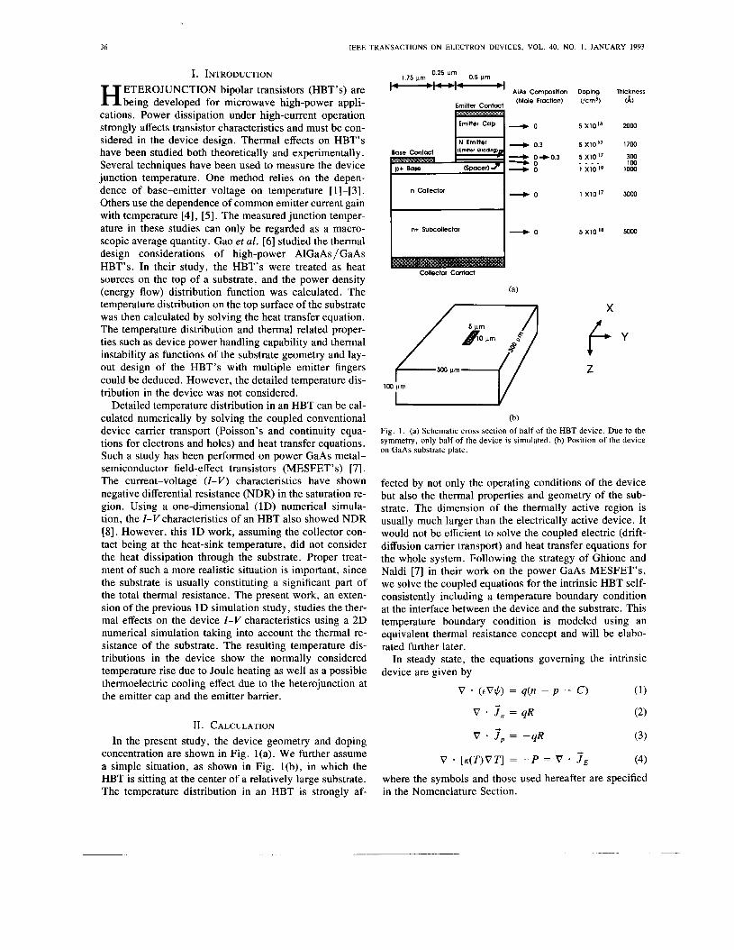
concentration are shown in Fig. l(a). We further assume a simple situation, as shown in Fig. l(b), in which the HBT is sitting at the center of a relatively large substrate. The temperature distribution in an HBT is strongly af-
175 pm 0’25 ‘um 0.5 pm
mw AlAs Composition Doping Em,tter contact (Mole Fraction) (/cm3)
-0 5 Xl0 ’8
+ 0.3 5 ~ 1 0 1 7
+ O e 0 . 3 5 X I O ” -0 -0 1 XlO’9
_ _ _ _
5 x10 n+ Subcollector
Collector Contact
(a)
Thickness CA,
2000
1700
300 100 I000
3000
5000
X
F Y Z
Fig. 1 . (a) Schematic cross section of half of the HBT device. Due to the symmetry, only half of the device is simulated. (b) Position of the device on GaAs substrate plate.
fected by not only the operating conditions of the device but also the thermal properties and geometry of the sub- strate. The dimension of the thermally active region is usually much larger than the electrically active device. It would not be efficient to solve the coupled electric (drift- diffusion carrier transport) and heat transfer equations for the whole system. Following the strategy of Ghione and Naldi [7] in their work on the power GaAs MESFET’s, we solve the coupled equations for the intrinsic HBT self- consistently including a temperature boundary condition at the interface between the device and the substrate. This temperature boundary condition is modeled using an equivalent thermal resistance concept and will be elabo- rated further later.
In steady state, the equations governing the intrinsic device are given by
v (EV$) = q(n - p - C ) (1)
V J , = qR (2)
V * J , = -qR (3)
V - [ K ( T ) V T ] = - P = V - 7, (4)
+
+
where the symbols and those used hereafter are specified in the Nomenclature Section.
LlOU et a l . : THERMAL EFFECTS ON THE CHARACTERISTICS OF AIGaA$/GaAs HBT’r
The general drift-diffusion model including the non- uniform spatial distributions of the energy band, degen- eracy factor, and temperature will be applied in the pres- ent study. The semiconductor current-flow equation including a temperature gradient term has been derived by Stratton [9]. The coefficient of this temperature gradient term depends on the free carrier relaxation time T which in turn is a function of the carrier energy above the band edge. Marshak [lo] has derived a generalized drift and diffusion current equation for heterostructure semicon- ductor. His calculation has resulted in two extra terms due to heterostructure in the electron and hole current equa- tions besides the conventional drift and diffusion terms. One term is proportional to the gradient of the electron affinity for the electron current, and the gradient of the sum of electron affinity and bandgap for the hole current. The other is proportional to the gradient of the equivalent density of states for the respective energy bands for the electron and hole currents. The electron and hole current densities J , and J p are given by
-+ J , = p,&kTVn -
kT VN, + p, - - - a,V 9 Nc
kT VN,, - p p - - + apv (F)
4 N ,
The first term on the right hand side (R
+*) 4
IS) of ( 5 ) and (6) is the diffusion component where the diffusion coefficient including the degeneracy factor is p.P,,,kT/q. The second term is the generalized drift component which is a summation of the contributions from the electric field, band structure, and temperature gradient. Assuming the free carrier relaxation time is proportional to the square root of the energy, the coefficients =
~FZ(~,,~)/FI(~,,~) in (5) and in (6) are obtained. The main temperature gradient in the AlGaAs /GaAs HBT device usually resides in the GaAs collector region, where the doping density is less than 2 X 10i7/cm3, and the polar- optical mode is the dominant scattering mechanism. A de- pendency of the relaxation time on the square root power of carrier energy is a reasonable approximation in this GaAs collector region [ 121. For the region where acoustic phonon scattering is the dominant scattering mechanism, the relaxation time is inversely proportional to the square root of the carrier energy, and a,,p = 2Fl(q,,,)/F0(q,,,), which were used in [I 11. For the region where the dom- inant scattering mechanism is the ionized impurity scat- tering, the relaxation time is proportional to the three halves power of the carrier energy, and a,,p = 4F3(7n,p) / F ~ ( q n , p ) .
31
One of the basic assumptions made in the drift-diffu- sion model is that the electrons and holes are in thermal equilibrium locally with the host lattice (heat loss due to radiation and convection with the ambient environment is not considered here). This assumption makes the semi- conductor, composed of the subsystems of free carriers and lattice, a thermodynamic system. Temperature, be- sides the quasi-Fermi levels for electrons and holes, is one of the dynamic variables. Using a rigorous thermo- dynamics treatment and without an explicit form for the heterostructure, Wachutka [ 131 is able to show similar electron and hole current equations as ( 5 ) and (6), where ka, / q and ka,, / q are the heterostructure-excluded ther- moelectric power associated with the electrons and holes. Modified slightly, his derivation for the heterostructure leads to the energy flow equation
7, = [ - [a , , kT + E,] 9 - K,VT
where 7, is the energy flow, K , and K~ are the thermal conductivities associated with electron gas and hole gas, respectively. The first term in the two braces on the RHS of (7) is the heuristic energy flow contribution of the elec- tron and hole currents. The remaining terms on the RHS take into account the heat flow associated with the tem- perature gradient. These temperature gradient terms after the operation of divergence, can be combined with K , the lattice thermal conductivity in (4). As discussed by the same author [ 131, K , and K~ are less than 1 % of K for the carrier concentration of less than lOI9/cm3, and there- fore, their contribution to the energy flow is neglected in the present calculation.
The adiabatic temperature condition is applied on the device boundary except at the bottom of the device where the temperature boundary condition is given by
where fi is the outwardly normal unit vector, To is the heat sink temperature, and Rth is the equivalent specific ther- mal resistance of the substrate. The left hand side (LHS) of (8) is the energy flow from the device into the sub- strate, while the RHS implements the equivalent thermal resistance concept. Rth can be calculated by taking into account the three-dimensional heat flow in the substrate. The calculation of Rth for the situation in Fig. l(b) is given in the Appendix.
It is important to implement accurate temperature de- pendence of the material parameters especially for ther- mal simulation. In this study, the hole mobility pp and electron mobilities pn in GaAs as functions of tempera- ture, electric field, and doping density are given by [14],
38 IEEE TRANSACTIONS ON ELECTRON DEVICES, VOL. 40, NO. I , JANUARY 1993
cm2/V - s 380(300/ i“)2.7
pp(T7 + NA’ = [l + 3.17 x lO-I7(ND + NA)]0.266(1 + IE1/1.95 x lo4)
where IEl is the magnitude of the electric field; NA and NO are the acceptor and donor doping densities; the low- field mobility is
PL(T NO + NA)
72OO(3OO / 7‘)2.3 - - cm2/V * s [ i + 5.51 x 1 0 - ’ ( ~ ~ + ~ ~ ) 1 ~ , ~ ~ ~
the saturation velocity is
usat = (1.28 - 0.00157‘) X lo7 cm/s
and the critical field is
simulate a successive bias point on the same I-V curve, the solution of the previous bias point was used as the initial guess value. The structure in the calculation was discretized into a mesh of 40 X 120 (N,, X N,) points. The required computer storage space is about 45 Mb. The simulation was run on a Convex C220 machine, and CPU time for one bias point in I-V characteristics ranges from 10 to 40 min depending on the current levels. Usually higher current level requires a larger number of the iter- ations, hence a longer computing time.
E, = (5.4 - T/215) kV/cm. 111. RESULTS AND DISCUSSION
pn in Al,Gal -,As is calculated by taking the weighted average of the mobilities in the r- and X-valleys. The weighting factors are the respective carrier populations in both valleys [ 151. p p in Al,Gal -,As is calculated by as- suming the validity of the relaxation time and linear re- sponse approximation, in which pp (Al,Ga, -,As) =
where mp* and rP are the hole effective mass and momen- tum relaxation time for holes, respectively. The detailed modeling of the electron and hole mobilities in AlGaAs can be found in [15]. The percentage distributions of the bandgap difference in conduction and valence-band dis- continuities between AlGaAs and GaAs were assumed to be 65% and 35% for the temperature range of interest in the present calculation. The other material parameters, such as the effective mass and equivalent density of states in the conduction and valence bands and the dielectric constants, were adopted from [ 161. The thermal conduc- tivities of GaAs and AlGaAs were taken from [17] and [ 181, respectively. The Shockley-Reed-Hall recombina- tion with a carrier lifetime of 1 x s, assumed tem- perature-independent, for both electrons and holes was implemented, while the surface recombination was not in- cluded.
A central finite difference discretization with nonuni- form interval was used. A fully coupled Newton-Raphson numerical method was applied to solve the electrical equations (1)-(3). To begin the simulation, a uniform temperature distribution was assumed. The energy flow was calculated from the solution of electrical equations, and was used in the heat transfer equation (4) for solving the temperature distribution. With the updated tempera- ture distribution, (1)-(3) were solved again. These pro- cedures were repeated until the difference between two successive temperature distributions at every discretized location was smaller than the preset values of 0.03 K for low current level and 0.3 K for high current level. To
The simulations were carried out on an AlGaAs /GaAs HBT using both the voltage and current boundary condi- tions applied on the base contacts [ 191. The calculations were done on the symmetric half of this emitter-mesa HBT shown in Fig. l(a). The heat-sink temperature was 300 K in the following calculations.
Using the voltage boundary condition at the base con- tact, the Gummel plot, i.e., the collector and base current densities I , and zb, as functions of base-emitter voltage Vb, for a fixed collector-emitter voltage V,, is shown in Fig. 2. V,, is fixed at 3 V in the isothermal simulation and is ranging from 1 to 5 V in the thermal simulation. In the region of I, of less than 10’ A/m, both thermal and iso- thermal results coincide due to insignificant temperature rise in that current range. As I, becomes larger than 10’ A/m, both I , and deviate from the isothermal results. For large V,,, as Vb, increases, the ideality factors for both I, and Zb can be much less than one before both currents reach saturation levels in which current stays almost con- stant. In this region, I, is mainly affected by the series resistance in the collector. Increase in V,, causes temper- ature rise in the collector region. As a result, collector resistance increases and saturation level for I, is slightly smaller when V,, is larger.
The dependence of differential current gain and cutoff frequency on the collector current density with V,, as the variable parameter are shown in Fig. 3(a) and (b). All the curves of the current gain show a maximum. The decrease in the isothermal current gain as I , increases beyond lo3 A/m is due to the Kirk effect or the base pushout effect. As V,, increases, the maximum differential current gain decreases and occurs at a lower I,. Two reasons may be used to explain this trend. One is that the threshold of the Kirk effect is proportional to the collector doping density as well as the electron saturation velocity in the collector space-charge region. The threshold level decreases as V,, increases, since the saturation velocity becomes reduced
LIOU et al.: THERMAL EFFECTS ON T H E CHARACTERISTICS OF AIGaAs/GaAs HBT's 39
104 I 1
Base - Emitter Voltage (Volts)
Fig. 2. The calculated Gummel plot. (-) is the isothermal thermal simulation results with V,, = 3 V . (---), (- . -), (- . . -), (- . . . -), and (. . .) are the thermal simulation results with V , , = 1, 2, 3 , 4, and 5 V, respectively.
sothermal
U v,, = 5 Volts lu 10' 102 103 i o 4
Collector Current Density (Aim)
(b) Fig. 3 . (a) The differential current gain as a function of collector current density with V,, as the variable parameter. (b) The cutoff frequency as a function of collector current density with V , , as the variable parameter. The isothermal results are also shown.
at higher temperature. The other factor causing the sig- nificant drop of the differential current gain in the high- current region is the reduction of the emitter injection ef- ficiency when the base-emitter junction temperature is high. The hole occupation probability would spread out in a wider energy range in the valence band at a higher temperature. As a result, the base current, mainly the thermionic emission-diffusion current in the emitter bar- rier, increases and the current gain drops [20], 1211. A similar trend in the cutoff frequency dependency on I , and V,, can also be explained by the Kirk effect with which the equivalent base width increases causing an increase in the base transit time. When V,, increases, the carrier transit time through the equivalent base and base-collec- tor space-charge region becomes larger due to a lower electron mobility at higher temperatures.
600 t E'
650
:'Vce = 5 Volts
1 ---
1000 2000 3000 4000 Collector Current Density ( A h )
Fig. 4. The maximum temperature in the device as a function of collector current density with V , , as the variable parameter.
The dependence of the maximum temperature in the de- vice on the collector current density with V,, at the vari- able parameter is illustrated in Fig. 4. As collector current increases, so do the power dissipation and device temper- ature. With respect to the maximum temperature in the device, if the rate of power dissipation increase exceeds that of the heat flow through the thermal resistance, the thermal instability (also known as thermal runaway, de- fined by dT,,,/dI, + w) occurs. The temperature may increase without limit until the device is destroyed. With the present numerical scheme, the simulation with a higher temperature rise requires a longer computation time. Con- vergent solutions were not obtained for the device with a maximum temperature larger than 580 K. By extrapolat- ing the curve for V,<, = 5 V in Fig. 4, the thermal runaway in the present case may occur around a collector current density of 2000 A / m (corresponding to 2 X lo5 A/cm2 of the current density for an emitter width of 1 pm). Ther- mal runaway for the device operated with a smaller V,, occurs at a higher collector current.
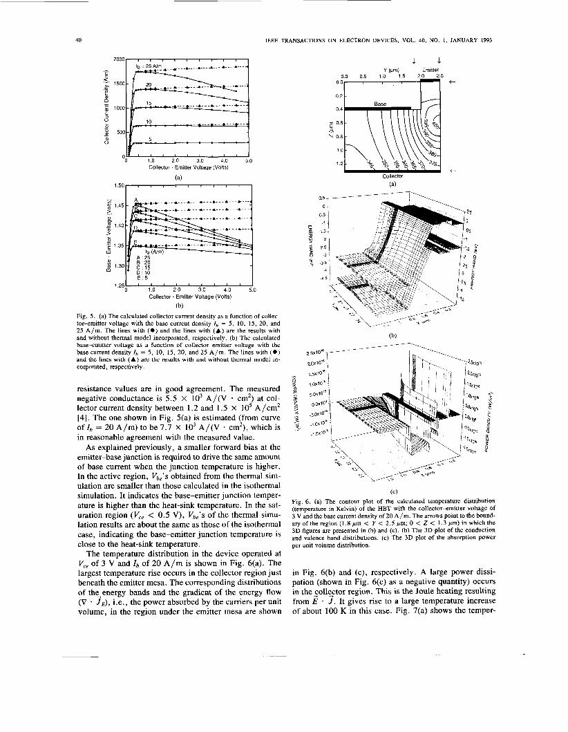
Using the current boundary condition, the HBT com- mon-emitter I-V characteristics are shown in Fig. 5(a). While the normal base modulation is observed utilizing the isothermal simulation, the NDR in the active region (i.e., V, , > 0.5 V) is produced by the thermal model. The NDR occurs mainly due to the reduction of carrier mo- bility as the temperature increases when the device is un- der high current operation. The corresponding base-emit- ter voltage V,,, as a function of collector-emitter V,, with the base current I,, as the variable parameter is shown in Fig. 5(b). The isothermal simulation results are also shown for comparison. For a constant base current, the thermal effects cause V, , to decrease as V,, increases in the active region. This inverse dependency of V,, on V,, has also been seen previously in Fig. 2. An HBT with the same structural parameters as shown in Fig. 1 has been fabricated. The thermal resistance of the device was mea- sured indirectly to be 2.9 K/mW [4]. Estimated from the simulation results of I , = 20 A / m and Vc, = 3 V, which gives a power of 38 mW, and the calculated maximum temperature rise of 100 K (see Fig. 6(a) in the following), the thermal resistance is about 2.6 K/mW. These thermal
40
2000, , I , I , I , I I I
IEEE TRANSACTIONS ON ELECTRON DEVICES, VOL. 40, NO. 1, JANUARY 1993
' 110 ' 210 ' i .0 ' 410 ' 510 Collector - Emitter Voltage (Volts)
(a) 1.50 ~ ~ ~ I I I I I I
E : 5
1.0 2.0 3.0 4.0 5.0 Collector - Emitter Voltage (Volts)
(b) Fig. 5 . (a) The calculated collector current density as a function of collec- tor-emitter voltage with the base current density Ib = 5 , 10, 15, 20, and 25 A/m. The lines with ( 0 ) and the lines with (A) are the results with and without thermal model incorporated, respectively. (b) The calculated base-emitter voltage as a function of collector-emitter voltage with the base current density I , = 5 , 10, 15, 20, and 25 A/m. The lines with ( 0 ) and the lines with (A) are the results with and without thermal model in- corporated, respectively.
resistance values are in good agreement. The measured negative conductance is 5 . 5 x lo3 A/(V cm2) at col- lector current density between 1.2 and 1.5 x lo5 A/cm2 [4]. The one shown in Fig. 5(a) is estimated (from curve of Ib = 20 A/m) to be 7.7 X lo3 A/(V cm2), which is in reasonable agreement with the measured value.
As explained previously, a smaller forward bias at the emitter-base junction is required to drive the same amount of base current when the junction temperature is higher. In the active region, Vbe's obtained from the thermal sim- ulation are smaller than those calculated in the isothermal simulation. It indicates the base-emitter junction temper- ature is higher than the heat-sink temperature. In the sat- uration region (Vce < 0.5 V), Vb,'S of the thermal simu- lation results are about the same as those of the isothermal case, indicating the base-emitter junction temperature is close to the heat-sink temperature.
The temperature distribution in the device operated at V,, of 3 V and zb of 20 A/m is shown in Fig. 6(a). The largest temperature rise occurs in the collector region just beneath the emitter mesa. The corresponding distributions of the_energy bands and the gradient of the energy flow (V .IE), i.e., the power absorbed by the camers per unit volume, in the region under the emitter mesa are shown
1 1 Y (um) Emitter
0.0 0.5 1.0 1.5 2.0 2.5 0.0 t
0.2
0.4
- 0.6 - 5 N 0.8
1 .o
1.2 t
Collector
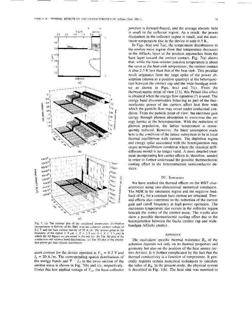
(c) Fig. 6. (a) The contour plot of the calculated temperature distribution (temperature in Kelvin) of the HBT with the collector-emitter voltage of 3 V and the base current density of 20 A/m. The arrows point to the bound- ary of the region (1.8 pm < Y < 2.5 pm; 0 < 2 < 1.3 pm) in which the 3D figures are presented in (b) and (c). (b) The 3D plot of the conduction and valence band distributions. (c) The 3D plot of the absorption power per unit volume distribution.
in Fig. 6(b) and (c), respectively. A large power dissi- pation (shown in Fig. 6(c) as a negative quantity) occurs in the_coll%ctor region. This is the Joule heating resulting from E J . It gives rise to a large temperature increase of about 100 K in this case. Fig. 7(a) shows the temper-
-
LIOU et ai : THERMAL EFFECTS ON THE CHARACTERISTICS OF AIGaA\/GaA\ HBT’\ 41
- 0 6 -
N 0.8 I 5
1 0 -
1.2
“’i 0 4 4 -
- il -+
Collector (a)
(C) Fig. 7. (a) The contour plot of the calculated temperature distribution (temperature in Kelvin) of the HBT with the collector-emitter voltage of 0.2 V and the base current density of 20 A / m . The arrows point to the boundary of the region (1.8 pm < Y < 2.5 p m ; 0 < Z < 1.3 pm) in which the 3D figures are presented in (b) and (c). (b) The 3D plot of the conduction and valence band distributions. (c) The 3D plot of the absorp- tion power per unit volume distribution.
ature contour for the device operated at Vce = 0.2 V and Zb = 20 A/m. The correspynding spatial distributions of the energy bands and V - J E in the cross section of the emitter mesa is shown in Fig. 7(b) and (c), respectively. Under this low applied voltage of V,.,, the base-collector
junction is forward-biased, and the average electric field is small in the collector region. As a result, the power dissipation in the collector region is small, and the max- imum temperature rise in the device is only 0.5 K.
In Figs. 6(a) and 7(a), the temperature distributions in the emitter mesa region show that temperature decreases in the AlGaAs layer as the position approaches from the base layer toward the emitter contact. Fig. 7(a) shows that, while the base-emitter junction temperature is about the same as the heat-sink temperature, the emitter contact is abut 2.5 K less than that of the heat sink. This peculiar result originates from the large spike of the power ab- sorption (shown as a positive quantity) at the heterojunc- tion between the emitter cap and the wide-bandgap emit- ter as shown in Figs. 6(c) and 7(c). From the thermodynamic point of view [ 131, this Peltier-like effect is obtained when the energy flow equation (7) is used. The energy band discontinuities behaving as part of the ther- moelectric power of the carriers affect heat flow with which the particle flow may occur under isothermal con- dition. From the particle point of view, the electrons gain energy through phonon absorption to overcome the en- ergy barrier at the heterojunction. With the reduction of phonon population, the lattice temperature is conse- quently reduced. However, the basic assumption made here is the condition of the lattice subsystem to be in local thermal equilibrium with carriers. The depletion region and energy spike associated with the heterojunction may create nonequilibrium condition where the classical drift- diffusion model is no longer valid. A more detailed treat- ment incorporating hot-carrier effects is, therefore, needed in order to further understand the possible thermoelectric cooling effect in the heterostructure semiconductor de- vices.
IV. SUMMARY We have studied the thermal effects on the HBT char-
acteristics using two-dimensional numerical simulation. The NDR in the saturation region and the negative feed- back of Vhe for a constant base current are obtained. Ther- mal effects also contribute to the reduction of the current gain and cutoff frequency at high-power operation. The maximum temperature rise occurs in the collector region beneath the center of the emitter mesa. The results also show a possible thermoelectric cooling effect due to the heterojunction between the GaAs emitter cap and wide- bandgap AlGaAs emitter.
APPENDIX The equivalent specific thermal resistance Rth of the
substrate depends not only on its thermal properties and geometry but also on the position of the heat source (ac- tive device). It is further complicated by the fact that the thermal conductivity is a function of temperature. It gen- erally requires certain numerical techniques to calculate the value of Rth. In the present study, the physical system is described in Fig. l(b). The heat sink was assumed to
IEEE TRANSACTIONS ON ELECTRON DEVICES, VOL. 40, NO. 1, JANUARY 1993 42
600
550 - Y
a, 500. 3
0
- 450 ’
400
350
be at the bottom of the substrate. The other surrounding surfaces are adiabatic, except for the heat source area. In this area, we assumed a uniform energy flow Q which is calculated from the average of total device power output
$ 7, A da
Q = (All 1, l y
where A is the outwardly normal unit vector, and 1, and ly are the x and y dimensions of the bottom area of the de- vice.
For the temperature-independent thermal conductivity case, the temperature distribution O(x, y , z) is given in the following:
.
.
.
2 m y QLly Ly KOLXL,
cos - + - (Z - d ) + To (A2)
where C ’ excludes the m = n = 0 term, and
mal, . naly sin - sin -, m, n # 0 4Q
amn = mna2KoYmn ~x ~y
mTK0 Ly L, 2Qly mal,
amo = ~ sin -
2Q1, naly aon = ~ sin -.
naKO L, Ly
The L,, Ly, and d are the x, y , and z dimensions of the substrate, respectively, and K~ is the thermal conductivity of the substrate at the heat-sink temperature. The Kirch- hoffs transformation can be made to account for a tem- perature-dependent thermal conductivity [22 ] . Using K ( T ) = ~~(T/300)-~, the corrected temperature T i s given by
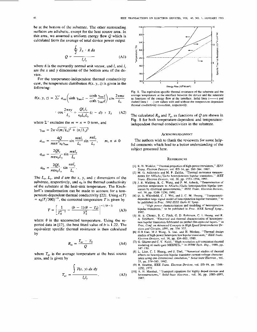
where 8 is the uncorrected temperature. Using the re- ported data in [17], the best fitted value of b is 1.22. The equivalent specific thermal resistance is then calculated by
where Ta, is the average temperature at the heat source area, and is given by
6501‘5
3001 lo 1 2 3 4
Energy Flow (105W/cmz)
Fig. 8. The equivalent specific thermal resistance of the substrate and the average temperature at the interface between the device and the substrate as functions of the energy flow at the interface. Solid lines (-) and dashed lines (---) are values with and without the temperature-dependent thermal conductivity correction, respectively.
The calculated Rth and Ta, as functions of Q are shown in Fig. 8 for both temperature-dependent and temperature- independent thermal conductivities in the substrate.
ACKNOWLEDGMENT
The authors wish to thank the reviewers for some help- ful comments which lead to a better understanding of the subject presented here.
REFERENCES
R. H. Winkler, “Thermal properties of high-power transistors,” IEEE Trans. Electron Devices, vol. ED-14, pp. 260-264, 1967. M. G. Adlerstein and M. P. Zaitlin, “Thermal resistance measure- ments for AlGaAs /GaAs heterojunction bipolar transistors,” IEEE Trans. Electron Devices, vol. 38, pp. 1553-1554, 1991. J . R. Waldrop, K. C. Wang, and P. M. Asbeck, “Determination of junction temperature in AlGaAs /GaAs heterojunction bipolar tran- sistors by electrical measurements,” IEEE Trans. Electron Devices, vol. 39, pp. 1248-1250, 1992. D. S. Whitefield, C. J. Wei, and J. C. M. Hwang, “Temperature- dependent large signal model of heterojunction bipolar transistor,” to be published in Proc. I992 IEEE GaAs IC Symp. -, “High power characterization and modeling of heterojunction bipolar transistors,” to be published in Proc. IEEE Sarnof Symp., 1992. M. E. Cheney, R. C. Fitch, G. D. Robinson, C. I. Huang, and R. A. Neidhard, “Electrical and thermal characteristics of heterojunc- tion bipolar transistors fabricated on peeled film epitaxial layers,” in Proc. Con6 on Advanced Concepts in High Speed Semiconductor De- vices and Circuits, 1991, pp. 334-337. G-B Gao, M-Z Wang, X. Gui, and H. Morkos, “Thermal design studies of high-power heterojunction bipolar transistors,” IEEE Trans. Electron Devices, vol. 36, pp. 854-863, 1989.
[7] G. Ghione and C. U. Naldi, “High-resolution self-consistent thermal modeling of multi-gate MESFETs,” in IEDM Tech. Dig. , 1989, pp.
[8] L. Liou, C. I. Huang, and J . Ebel, “Numerical studies of thermal effects on heterojunction bipolar transistor current-voltage character- istics using one-dimensional simulation,” Solid-State Electron., vol.
[9] R . Stratton, IEEE Trans. Electron Devices, vol. ED-19, pp. 1288- 1292, 1972.
[lo] A. H. Marshak, “Transport equations for highly doped devices and heterostructures,” Solid-State Electron., vol. 30, pp. 1089-1093, 1987.
147- 150.
35, pp. 579-585, 1992.
LIOU et al.: THERMAL EFFECTS ON T H E CHARACTERISTICS OF AIGaAs/GaAs HBT’s 43
1111 G. H. Song, K. Hess, T. Kerkhoven, and U. Ravaioli, “Two-dimen- sional simulator for semiconductor lasers,” in IEDM Tech. Dig . ,
[I21 D. C . Look, Electrical Characterization of GaAs Materials und De- vices.
1131 G. K. Wachutka, “Rigorous thermodynamic treatment of heat gen- eration and conduction in semiconductor device modeling,” IEEE Trans. Computer-Aided Des. , vol. 9 , pp. 1141-1149, 1990.
1141 J. S. Blakemore, “Semiconducting and other major important prop- erties of gallium arsenide,” J . Appl. Phys., vol. 53, pp. R123-Rl81, 1982.
1151 R. J . Schuelke, “Numerical simulation of semiconductor hetero- structure,” Ph.D. dissertation, Purdue University, West Lafayette, IN, 1984.
1161 S. Adachi, “GaAs, AIAs, and AI,Ga, - ,As: Material parameters for use in research and device application,” J . Appl. Phys., vol. 58, pp.
1171 P. D. Maycock, “Thermal conductivity of silicon, germanium, 111-V compounds and 111-V alloys,” Solid-State Electron., vol. 10, pp. 161- 168, 1967.
[181 M. A. Afromowitz, “Thermal conductivity of Ga, -.rAI,As alloys,”
[I91 L. L. Liou, J . Ebel, and C . I . Huang, “DC transistor characteristics of mesa-etched-emitter heterojunction bipolar transistors using two dimensional simulation with current boundary condition,” in Proc. NASECODE VII, 1991, pp. 241-242.
1201 G. B. Gao, Z. F. Fan, and H . Morkoq, “Negative output differential resistance in AlGaAs/GaAs heterojunction bipolar transistors, ” Appl. Phys. Lett., vol. 61, pp. 198-200, 1992.
[21] J . F. Palmier, J . Dangla, E. Caquot, and M. Campana, “Numerical simulation of electrical transport in 111-V microstructure devices,” in Proc. NASECODE I Conf. , 1985, pp. 70-82.
1989, pp. 143-146.
New York: Wiley, 1989, pp. 83-85.
Rl-R29, 1985.
J . Appl. Phys. , vol. 44, pp. 1292-1294, 1973.
[22] W. B. Joyce, “Tb dependent conducti 1975.
.. iermal resistance of heat sinks with temperature- vity,” Solid-StateElectron., vol. 18, pp. 321-322,
Lee L. Liou (S’82-M’87) was born in Taipei, Taiwan, in 1954. He received the B.S. degree in physics from National Tsing-Hua University, Hsin-Chu, Taiwan, in 1976, the M.S. degree in geophysics from National Taiwan University, Taipei, Taiwan, in 1978, and the Ph.D. degree in physics from University of Southern California, Los Angeles, in 1985.
From1985 to 1986, he was with Hewlett-Pack- ard Fort Collins Integrated Circuit Division, Ft. Collins, CO, where he was responsible for ad-
vanced CMOS metrology development. From 1987 to 1989, he was with Universal Energy System Inc., Dayton, OH, where he was involved in the development of the advanced heterojunction devices for high-speed com- muniction applications. Since 1990, he has been with Solid-state Electron- ics Directorate, Wright Laboratory, Wright-Patterson Air Force Base, OH. He is presently working on the modeling of power heterojunction bipolar transistors.
John L. Ebel received the B.S. and M.Eng. de- grees in electrical engineering from Cornell Uni- versity, Ithaca, NY, in 1984 and 1985, respec- tively.
He was commissioned a 2nd Lieutenant in the Air Force in 1984, and was stationed at the Avionics Laboratory at Wright-Patterson Air Force Base with the Design Group of the Micro- electronics Branch through February 1989. Dur- ing that time, he worked on development CAD tools, languages (VHDL), and environments as
part of the Very High Speed Integrated Circuits Program (VHSIC). He is currently working towards the Ph.D. degree at Carnegie Mellon Univer- sity, Pittsburgh, PA.
Chern I. Huang (M’74) was born in Taiwan in 1940 He received the B S.E.E. degree from Na- tional Cheng-Kung University, Talwan, in 1962, the M.S.E E. degree from Iowa State University, Ames, in 1967, and the Ph.D degree in electncal engineering from University of Flonda, Gaines- ville, in 1973.
He had worked for Collins Radio Company and Bendix Avionics Division between 1966 and 1969. Since 1973, he has been with the Matenals, Avionics, and Solid State Electronics Director-
ates, Air Force Wnght Laboratory, Wright-Patterson Air Force Base, OH, on vanous assignments: in-house research, project management, and ad- ministrative duties. His research and development interests have been in compound semiconductor matenals, device physics and modeling, and cir- cuits for microwave and digital applications.