Abstract—Thermal test structures and ring oscillators (ROs)are fabricated in 0.18-μm three-dimensional (3-D)–SOI technol-ogy. Measurements and electrothermal simulations show that ther-mal and parasitic effects due to 3-D packaging have a significantimpact on circuit performance. A physical thermal model is pa-rameterized to provide better prediction of circuit performancein 3-D technologies. Electrothermal simulations using the thermalmodel show good agreement with measurement data; the model isapplicable for different circuits designed in the 3-D–SOI technol-ogy. By studying the phase noise of ROs, the device noise proper-ties of 3-D–SOI technology are also characterized and comparedwith conventional bulk CMOS technology.
THREE-DIMENSIONAL (3-D) integrated-circuit technol-ogy offers the ability to stack die in the vertical dimension,
and there is recent work using this technology to improve sys-tem performance [1]–[5]. By utilizing the vertical dimension,wiring lengths and chip sizes can be reduced. These reductionskeep signal propagation delay and power consumption due tointerconnections under control as the LSI capacity increases.Therefore, 3-D technology can be used to achieve large-scaleintegration with high performance and low power consumption.However, thermal and packaging effects need to be addressedbefore utilizing any 3-D technology, as these effects impactboth system architecture and circuit design [6]. Furthermore,little is known about how thermal and packaging effects impactdevice noise characteristics in emerging 3-D technologies.
Manuscript received September 9, 2008; revised January 5, 2009. Firstpublished February 27, 2009; current version published March 25, 2009. Thereview of this paper was arranged by Editor M. J. Deen.
T. W. Chen is with the Center for Integrated Systems, Stanford University,Stanford, CA 94305 USA (e-mail: [email protected]).
J.-H. Chun is with the Department of Semiconductor Systems Engineering,SungKyunKwan University, Suwon 440-746, Korea.
Y.-C. Lu is with the Graduate Institute of Electronics Engineering andthe Department of Electrical Engineering, National Taiwan University, Taipei10617, Taiwan.
R. Navid is with True Circuits, Inc., Los Altos, CA 94022 USA.W. Wang is the with Department of Electrical Engineering, Stanford Univer-
sity, Stanford, CA 94305 USA.C.-L. Chen is with the Lincoln Laboratory, Massachusetts Institute of
Technology, Lexington, MA 02420-9108 USA.R. W. Dutton is with the Center for Integrated Systems, Stanford University,
Stanford, CA 94305 USA (e-mail: [email protected]).Color versions of one or more of the figures in this paper are available online
at http://ieeexplore.ieee.org.Digital Object Identifier 10.1109/TED.2009.2014188
Fig. 1. Cross section of 3-D–SOI technology (not shown to scale).
There are many types of 3-D integrated-circuit technologieswhich are actively being studied, including monolithic [7],stacked-chip [8], and stacked-wafer [6] 3-D integrated circuits.All the circuits discussed in this paper are implemented withstacked-wafer 3-D technology, offered by the Lincoln Labo-ratory, Massachusetts Institute of Technology (MIT). In this0.18-μm technology, three wafers using fully depleted SOI arebonded with interconnects using through-wafer vias [6]. Theintegrated-circuit layers are labeled Tier A (A), Tier B (B), andTier C (C), with Tier A closest to the 675-μm-thick substrate,as shown in Fig. 1.
This paper presents our findings on the thermal and packag-ing effects, as well as device noise characterization, obtainedfrom a 3-D multiproject run offered by the Lincoln Laboratory.
The purpose of this paper is twofold. First, a physics-basedthermal model will be presented. The parameters of this modelwere extracted from the thermal test structures and verified witha separate set of test structures from another research group [9].It is also demonstrated that this model is applicable for the elec-trothermal simulations of different circuits. As an applicationexample of the thermal model, the electrothermal simulationof ring oscillators (ROs) fabricated using 3-D–SOI technologyis presented. Second, device noise characterization was donefor 3-D–SOI devices with various geometric parameters. Thedevice noise performance is then compared with a single-chipconventional 0.18-μm bulk CMOS process.
II. THERMAL AND PACKAGING EFFECTS IN
3-D–SOI TECHNOLOGY
Although the same structure is implemented on all three tiers,the performance is not the same for all tiers because of thermaland/or parasitic effects of 3-D stacking. In this paper, the3-D–SOI test chip is wire bonded to an unsealed package to
Authorized licensed use limited to: Stanford University. Downloaded on September 27, 2009 at 18:54 from IEEE Xplore. Restrictions apply.
CHEN et al.: THERMAL MODELING AND DEVICE NOISE PROPERTIES OF THREE-DIMENSIONAL–SOI TECHNOLOGY 657
Fig. 2. (a) Ids–Vds curve of 3-D–SOI NMOS, with VGS of 1.5 V. W/L =6 μm/0.2 μm. The performance degradation of Tiers B and C is mainly due tothermal effects. (b) I–V curve of a 3-D–SOI diode. Performance degradation ofTiers A and B is due to 3-D packaging (through-wafer vias) and other parasiticresistive effects.
study these effects. Our proposed intrinsic model then can befurther integrated to different packaging models, includingthose using advanced cooling technologies. It should be notedthat models of different advanced cooling technologies are notdiscussed here, since they are beyond the scope of this paper;Fig. 2(a) shows the measured Ids–Vds characteristics of aMOSFET implemented on all three tiers. Note that Tier Ahas the highest drive current while Tier C has the lowest drivecurrent.
Fig. 2(b) shows the measured I–V characteristics of diodesfrom the same 3-D circuit. Note that the Tier-C diode now hasthe highest current, and that of Tier A has the lowest. This trendis opposite to that shown in Fig. 2(a). The physical cause ofthis difference can be traced back to the thermal and packagingeffects in the 3-D–SOI technology.
The MOSFET performance degradation shown in Fig. 2(a)could be mainly due to thermal-induced mobility reduction.Without losing its generality, the saturation current expressionfor a MOSFET can be approximated by
IDSat =WμCox
2L(VGS − VT )2
=WμCox
2L(VG − IDSat · RSParasitic − VT )2 (1)
where RSParasitic is the parasitic resistance between the sourcepad to the source terminal of the transistor. For this test struc-ture, RSParasitic is a few ohms and IDSat is a few milliamperes;therefore, the packaging effects are negligible. However, carriermobility μ decreases considerably with increasing temperatureT and the effective mass of an electron m∗, following [10]:
μ =√
8πqh4C11
3Eds(m∗)5/2(kT )3/2∝ (m∗)−5/2(T )−3/2. (2)
Although the threshold voltage decreases at higher tempera-tures, the effect of mobility lowering still dominates, resultingin an IDSat decrease with increasing temperature. It follows thatthe transistor on Tier A has the highest IDSat, while Tier C hasthe lowest, as shown in Fig. 2(a).
Diode performance degradation due to 3-D packaging andparasitic resistive effects is shown in Fig. 2(b). The diodecurrent can be expressed as
IDiode = I0
(e
qVAkT − 1
)
= I0
(e
q(VPad−IDiode·RParasitic)kT − 1
). (3)
For this test structure (with reference to Fig. 1), the productof IDiode and RParasitic is significant because IDiode in Fig. 2(b)is much larger than IDS in Fig. 2(a), and the IDiode × RParasitic
product has an exponential effect on IDiode. For this test struc-ture, this effect dominates over the increase of the intrinsiccarrier density as temperature increases. This is the reasonfor Tier A having the lowest diode current and Tier C thehighest, as shown in Fig. 2(b). Parasitic resistance of eachthrough-wafer via is independently measured to be approxi-mately 3 Ω. The current degradation of the diodes, as shownin Fig. 2(b), may be explained by parasitic resistances of thismagnitude.
These effects on circuit performance show opposite trends.Therefore, both thermal modeling and parasitic extraction arerequired for an electrothermal simulator to help circuit design-ers better predict actual circuit performance.
III. THERMAL MODELING AND
ELECTROTHERMAL SIMULATIONS
A. Experiments
An N-type MOSFET is surrounded by diode-connectedMOSFETs, which act as on-chip heat sources to control thetemperature of this device under test (DUT). The DUT hasfour connections to the gate, which can be used to accuratelymeasure the gate resistance [11]. The test chip is first placed ina hot chamber, and the temperature dependence of the polysil-icon gate resistance is calibrated in an enclosed temperature-controlled environment, as shown in Fig. 3. The test chip isthen placed in ambient, and on-chip heat sources are used tocontrol the DUT temperature. Changes in gate resistance canthen be used to determine the temperature when the on-chipheat sources are turned on. The effects of process variationeffects were taken into account by calibrating each gate resistor
Authorized licensed use limited to: Stanford University. Downloaded on September 27, 2009 at 18:54 from IEEE Xplore. Restrictions apply.
658 IEEE TRANSACTIONS ON ELECTRON DEVICES, VOL. 56, NO. 4, APRIL 2009
Fig. 3. Mapping of gate resistance as a function of temperature. With thischaracterization, the gate resistance can be used to determine temperature whenthe on-chip heat sources are turned on. The transistor shown has W/L =6 μm/0.2 μm, and is on Tier C. Figure shown is a typical measurement. Eachgate resistor is calibrated individually.
Fig. 4. (a) Layout of the DUT and the heat sources on each tier. Temperatureof DUT can be controlled with surrounding heat sources. DUT gate resistanceis used as a thermometer. (b) Three-dimensional view of test structures. Teststructures are stacked on top of one another and can be turned on or offindividually to simulate different operating conditions.
individually. The layout of the DUT and heat sources are shownin Fig. 4.
The thermal time constant for the self-heating of each tiercan be determined with this test structure by using the acoutput conductance technique [12]. The gate of the DUT is firstbiased to Vdd. An impedance analyzer is then used to applyboth a dc bias and an ac signal with varying frequencies at
Fig. 5. Thermal test structure independently designed by the research groupat the Lincoln Laboratory [9]. Note that this test structure is approximately fourtimes larger than the thermal test structure in Fig. 4(a).
the drain. The drain admittance can then be measured as afunction of frequency. The drain admittance starts out negativeat low frequencies and then eventually becomes positive as thefrequency increases. This is due to the suppression of ac self-heating at higher frequencies. In this way, the thermal timeconstant may be experimentally determined. The results areshown in Fig. 6.
In this paper, thermal test structures described earlier werefabricated in order to develop a physics-based thermal modelthat can be experimentally verified.
A separate set of thermal test structures was used to validatethe thermal model presented in this paper [9]. As shown inFig. 5, this test structure is entirely different from the teststructure used in this paper, including different layout areas[∼522 μm2 for Fig. 4(a) versus ∼2400 μm2 for Fig. 5], heatsources (diode-connected transistors versus resistors), and ther-mal sensors (polysilicon gate resistors versus diodes). As shownin Fig. 5, in this test structure [9], four SOI active resistors areplaced near a diode which is used as a thermometer. This teststructure was replicated in each of the three tiers. Voltages werethen applied to the resistors, and the diode current was used asa temperature sensor. Temperature measurements were madefor all three tiers. The thermal model presented in this papermatches the temperature measurements made by the researchgroup at Lincoln Laboratory, as will be presented in the nextsection.
This thermal model was then implemented in an elec-trothermal simulator, which was used to predict the actualcircuit performance of ROs fabricated on the same chip(Section III-C). These same oscillators were also used to quan-tify device noise (Section IV).
B. Thermal Modeling
A physical lumped thermal model is shown in Fig. 6, andthe model parameters can be extracted using measurementdata collected from the thermal test structure shown in Fig. 4.This lumped model assumes an average tier temperature. Thisassumption holds because the test circuit is designed to be smallcompared with the geometrical scale for thermal conductionand also because the thermal conductivity of silicon is muchlarger than that of silicon dioxide. Therefore, the temperatureprofile across the tiers is more significant than the profile withina tier.
The thermal model is also verified, using thermal test struc-tures independently designed by the Lincoln Laboratory, to beapplicable for different circuits. A single known temperature
Authorized licensed use limited to: Stanford University. Downloaded on September 27, 2009 at 18:54 from IEEE Xplore. Restrictions apply.
CHEN et al.: THERMAL MODELING AND DEVICE NOISE PROPERTIES OF THREE-DIMENSIONAL–SOI TECHNOLOGY 659
Fig. 6. Thermal model used in this paper. Power is the I × V product, andthermal resistances are shown.
at a given power consumption level from the measured datais required to calibrate the thermal model (Fig. 7). Calibrationis needed to reconcile measurement errors and experimentaldeviations for model assumptions made by both teams. TheLincoln Laboratory team designed a larger test structure, usingresistors as heating elements and diodes as thermal sensors. Aheated chuck was also used to control the external temperature.In contrast, the test structure described in this paper usesdiode-connected transistors as heating elements and polysilicongate resistors as thermal sensors. The gate resistances weremeasured using four-point measurements to ensure accuracy,and a hot chamber is used to control external conditions. Giventhe differences in the test structure designs and measurementsetups of both teams, it is not surprising that a single cali-bration point is needed to reconcile both sets of measurementresults.
Fig. 8 shows the measured temperature data, together withthe temperature predicted by the thermal model presented inthis paper. It is worthwhile to note here that more poweris required to raise the temperature using the Lincoln Lab-oratory test structures than the test structures presented heresince they are approximately four times larger than the teststructures shown in Fig. 4(a). Nevertheless, the thermal modelpresented in this paper uses area as a parameter and is ableto account for different layout areas. The agreement betweenthe measured temperature data using two independently de-signed thermal test structures verifies that the thermal modelis applicable for different circuits designed using the 3-D–SOItechnology.
Fig. 7. Figures comparing temperatures predicted by thermal model withmeasured temperatures. (a) Only one tier active at any one time. (b) All threetiers active at the same time.
Fig. 8. Comparison of temperatures predicted by thermal model with mea-sured temperatures using the thermal test structures designed by the researchgroup at the Lincoln Laboratory. Note that the measured data agree well withthe results predicted by the thermal model although the power used in thiscircuit is much larger than the power used in the Stanford test structures (Fig. 7).
As an application example, the thermal model will be usedto perform electrothermal simulations with asymmetric ROsdesigned for device noise measurements.
Authorized licensed use limited to: Stanford University. Downloaded on September 27, 2009 at 18:54 from IEEE Xplore. Restrictions apply.
660 IEEE TRANSACTIONS ON ELECTRON DEVICES, VOL. 56, NO. 4, APRIL 2009
Fig. 9. Electrothermal simulations compared against measured oscillationfrequencies for all three tiers. Only one oscillator is turned on at any one timefor (a) 1×. (b) 3×.
C. Electrothermal Simulations
Asymmetric ROs were fabricated on this test chip primar-ily to measure device noise [13]. However, since oscillationfrequency is a function of oscillator temperature, these oscilla-tors can also be used to verify electrothermal simulation results.The design of the ROs will be explained in Section IV, wherethe device noise is discussed.
Three different asymmetric ROs with minimum channellengths of 0.18 μm (1×), 0.54 μm (3×), and 1.08 μm (6×)are fabricated on each tier, resulting in a total of nine ROs.
Electrothermal simulations were performed to predict theoscillation frequencies of ROs implemented on different tiers.The temperature beneath the substrate and the temperature ofthe air far above the test chip are set to be ambient. Thesetwo boundary conditions mirror the experimental setup and arebuilt into the thermal model. It is expected that both thermaland parasitic packaging effects will affect circuit performance.However, the exact operating conditions, under which each typeof effect dominates, are unknown. Electrothermal simulationscan help to gain design intuition.
For the first set of experiments, only one oscillator is turnedon at any one time. Fig. 9 shows measured oscillation frequen-cies and simulation results.
Fig. 10. Electrothermal simulations compared against measured oscillationfrequencies for all three tiers. All oscillators are turned on at the same time for(a) 1×. (b) 3×.
For the second set of experiments, all oscillators are turnedon at the same time. Measurements and simulation results areshown in Fig. 10. In Figs. 9 and 10, “No compensation” is theidealistic (and most unrealistic) case when neither thermal norparasitic resistive effects are considered. “Parasitic Effect only”is when the temperature is set to 25 ◦C for all tiers. “ThermalEffect only” is for parasitic resistances set to zero. “Electrother-mal simulation” considers both thermal and parasitic resistiveeffects.
Fig. 9 shows the situation when only one tier is active atany one time. For this case, Tier C has the lowest oscillationfrequency for the 1× oscillators [Fig. 9(a)], and Tier A hasthe lowest oscillation frequency for the 3× [Fig. 9(b)] and 6×oscillators (not shown). This is due to thermal effects beingdominant in 1× oscillators, and 3-D packaging effects beingdominant in 3× and 6× oscillators. Thermal effects are domi-nant in 1× oscillators as they have a smaller area over which todissipate heat through conduction. From Fig. 2(a), drive currentis lowest on Tier C when thermal effects are dominant. Note thatlower drive current translates to a lower oscillation frequency.It follows that Tier C has the lowest oscillation frequency for1× oscillators, as observed in Fig. 9(a).
Authorized licensed use limited to: Stanford University. Downloaded on September 27, 2009 at 18:54 from IEEE Xplore. Restrictions apply.
CHEN et al.: THERMAL MODELING AND DEVICE NOISE PROPERTIES OF THREE-DIMENSIONAL–SOI TECHNOLOGY 661
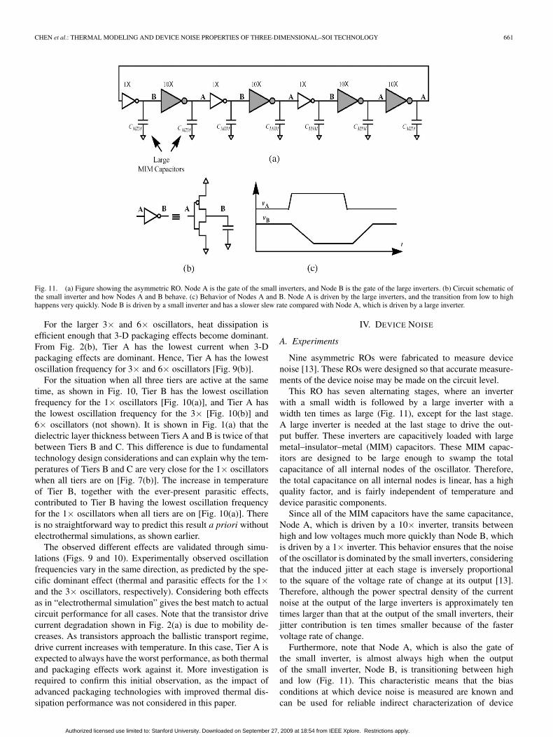
Fig. 11. (a) Figure showing the asymmetric RO. Node A is the gate of the small inverters, and Node B is the gate of the large inverters. (b) Circuit schematic ofthe small inverter and how Nodes A and B behave. (c) Behavior of Nodes A and B. Node A is driven by the large inverters, and the transition from low to highhappens very quickly. Node B is driven by a small inverter and has a slower slew rate compared with Node A, which is driven by a large inverter.
For the larger 3× and 6× oscillators, heat dissipation isefficient enough that 3-D packaging effects become dominant.From Fig. 2(b), Tier A has the lowest current when 3-Dpackaging effects are dominant. Hence, Tier A has the lowestoscillation frequency for 3× and 6× oscillators [Fig. 9(b)].
For the situation when all three tiers are active at the sametime, as shown in Fig. 10, Tier B has the lowest oscillationfrequency for the 1× oscillators [Fig. 10(a)], and Tier A hasthe lowest oscillation frequency for the 3× [Fig. 10(b)] and6× oscillators (not shown). It is shown in Fig. 1(a) that thedielectric layer thickness between Tiers A and B is twice of thatbetween Tiers B and C. This difference is due to fundamentaltechnology design considerations and can explain why the tem-peratures of Tiers B and C are very close for the 1× oscillatorswhen all tiers are on [Fig. 7(b)]. The increase in temperatureof Tier B, together with the ever-present parasitic effects,contributed to Tier B having the lowest oscillation frequencyfor the 1× oscillators when all tiers are on [Fig. 10(a)]. Thereis no straightforward way to predict this result a priori withoutelectrothermal simulations, as shown earlier.
The observed different effects are validated through simu-lations (Figs. 9 and 10). Experimentally observed oscillationfrequencies vary in the same direction, as predicted by the spe-cific dominant effect (thermal and parasitic effects for the 1×and the 3× oscillators, respectively). Considering both effectsas in “electrothermal simulation” gives the best match to actualcircuit performance for all cases. Note that the transistor drivecurrent degradation shown in Fig. 2(a) is due to mobility de-creases. As transistors approach the ballistic transport regime,drive current increases with temperature. In this case, Tier A isexpected to always have the worst performance, as both thermaland packaging effects work against it. More investigation isrequired to confirm this initial observation, as the impact ofadvanced packaging technologies with improved thermal dis-sipation performance was not considered in this paper.
IV. DEVICE NOISE
A. Experiments
Nine asymmetric ROs were fabricated to measure devicenoise [13]. These ROs were designed so that accurate measure-ments of the device noise may be made on the circuit level.
This RO has seven alternating stages, where an inverterwith a small width is followed by a large inverter with awidth ten times as large (Fig. 11), except for the last stage.A large inverter is needed at the last stage to drive the out-put buffer. These inverters are capacitively loaded with largemetal–insulator–metal (MIM) capacitors. These MIM capac-itors are designed to be large enough to swamp the totalcapacitance of all internal nodes of the oscillator. Therefore,the total capacitance on all internal nodes is linear, has a highquality factor, and is fairly independent of temperature anddevice parasitic components.
Since all of the MIM capacitors have the same capacitance,Node A, which is driven by a 10× inverter, transits betweenhigh and low voltages much more quickly than Node B, whichis driven by a 1× inverter. This behavior ensures that the noiseof the oscillator is dominated by the small inverters, consideringthat the induced jitter at each stage is inversely proportionalto the square of the voltage rate of change at its output [13].Therefore, although the power spectral density of the currentnoise at the output of the large inverters is approximately tentimes larger than that at the output of the small inverters, theirjitter contribution is ten times smaller because of the fastervoltage rate of change.
Furthermore, note that Node A, which is also the gate ofthe small inverter, is almost always high when the outputof the small inverter, Node B, is transitioning between highand low (Fig. 11). This characteristic means that the biasconditions at which device noise is measured are known andcan be used for reliable indirect characterization of device
Authorized licensed use limited to: Stanford University. Downloaded on September 27, 2009 at 18:54 from IEEE Xplore. Restrictions apply.
662 IEEE TRANSACTIONS ON ELECTRON DEVICES, VOL. 56, NO. 4, APRIL 2009
Fig. 12. Figure showing phase noise of asymmetric RO measured at the 1/f2
region.
noise through phase noise measurements for various biasvoltages.
Three different asymmetric ROs with minimum channellengths of 0.18 μm (1×), 0.54 μm (3×), and 1.08 μm (6×) arefabricated on each of the three tiers, resulting in nine differentoscillators.
Device noise is characterized by measuring the phase noiseof the ROs in the 1/f2 region, as shown in Fig. 12. In thisregion, the 1/f noise of the device does not affect the devicenoise. Furthermore, there is a one-to-one correspondence of thephase and device noises in the 1/f2 region.
B. Discussion of Device Noise
Phase noise is a function of power and oscillation frequency.Therefore, comparing absolute phase noise across ROs withoutregard for power consumption and oscillation frequency ismeaningless. This is because different ROs have different oscil-lation frequencies and consume different power, although theymight be nominally designed to be the same. Process variationsalso cause performance differences between nominally similaroscillators.
Delta phase noise (DPN, Fig. 13) is the difference betweenthe measured phase noise and the minimum achievable phasenoise PNmin(Δf) [14], [15]
PNmin(Δf) ≈ 7.33f0kT
NCν2dd(Δf)2
=7.33kT
Pmin
(f0
Δf
)2
(4)
where Pmin = f0NCν2dd, f0 is the nominal oscillation fre-
quency, Δf is the offset frequency, N is the number of stagesin the RO, C is the capacitance of each stage, and νdd is thesupply voltage.
As shown in (4), the minimum achievable phase noise com-pensates for differences in power consumption and oscilla-tion frequencies across ROs. Therefore, DPN, which is thedifference between the measured phase noise for a particularoscillator and the minimum achievable phase noise of the sameoscillator, compensates for differences in power consumptionand oscillation frequencies of different oscillators. Thus, it isa figure of merit for measuring device noise [14], [15]. LowerDPN indicates better device noise performance.
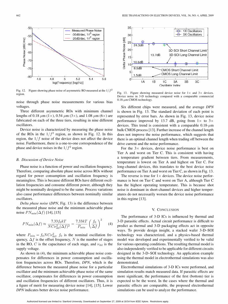
Fig. 13. Figure showing measured device noise for 1× and 3× devices.Device noise in 3-D technology compared with a comparable commercial0.18-μm CMOS technology.
Six different chips were measured, and the average DPNis shown in Fig. 13. The standard deviation of each point isrepresented by error bars. As shown in Fig. 13, device noiseperformance improved by 13.7 dB, going from 1× to 3×devices. This trend is consistent with a comparable 0.18-μmbulk CMOS process [13]. Further increase of the channel lengthdoes not improve the noise performance, which suggests thatthere is an optimal channel length when trading off between thedrive current and the noise performance.
For the 3× devices, device noise performance is best onTier A and worst on Tier C. This is consistent with havinga temperature gradient between tiers. From measurements,temperature is lowest on Tier A and highest on Tier C. Forlong-channel devices, this translates to the best device noiseperformance on Tier A and worst on Tier C, as shown in Fig. 13.
The reverse is true for 1× devices. The device noise perfor-mance is best on Tier C and worst on Tier A, although Tier Chas the highest operating temperature. This is because shotnoise is dominant in short-channel devices and higher temper-atures do not necessarily worsen the device noise performancein this regime [13].
V. CONCLUSION
The performance of 3-D ICs is influenced by thermal and3-D parasitic effects. Actual circuit performance is difficult topredict as thermal and 3-D packaging effects act in oppositeways. To provide design insight, a stacked wafer 3-D–SOItechnology was characterized, and a physics-based thermalmodel was developed and experimentally verified to be validfor various operating conditions. The resulting thermal model isalso independently verified to be applicable for different circuitsdesigned in the 3-D–SOI technology. An application exampleusing the thermal model in electrothermal simulations was alsodemonstrated.
Electrothermal simulations of 3-D ICs were performed, andsimulation results match measured data. If parasitic effects aremore significant, the performance of the first (bottom) tier isexpected to be the worst. In the cases where the thermal andparasitic effects are comparable, the proposed electrothermalsimulations can be used to analyze the performance.
Authorized licensed use limited to: Stanford University. Downloaded on September 27, 2009 at 18:54 from IEEE Xplore. Restrictions apply.
CHEN et al.: THERMAL MODELING AND DEVICE NOISE PROPERTIES OF THREE-DIMENSIONAL–SOI TECHNOLOGY 663
Device noise measured for this technology shows the sametrends as a conventional 0.18-μm bulk CMOS technology.Measurement data are also consistent with having a temper-ature gradient between tiers for long-channel devices. Highertemperatures do not necessarily degrade the noise performancein short-channel devices, as shot noise is dominant.
ACKNOWLEDGMENT
The authors would like to thank DARPA for the supportfor 3-D IC projects at both Stanford University and LincolnLaboratory, MIT. The authors would also like to thank key con-tributors to the 3-D fabrication process at Lincoln Laboratory,including J. A. Burns, C. K. Chen, J. M. Knecht, K. Warner,and D.-R. W. Yost.
REFERENCES
[1] T. W. Chen, J. H. Chun, Y. C. Lu, R. Navid, W. Wang, and R. W. Dutton,“Thermal modeling and device noise properties of 3D–SOI technology,”in Proc. Int. SOI Conf., Oct. 2007, pp. 89–90.
[2] E. Culurciello and P. Weerakoon, “Three-dimensional photodetectorsin 3-D silicon-on-insulator technology,” IEEE Electron Device Lett.,vol. 28, no. 2, pp. 117–119, Feb. 2007.
[3] G. L. Loi, B. Agrawal, N. Srivastava, S. Lin, T. Sherwood, andK. Banerjee, “A thermally-aware performance analysis of verticallyintegrated (3-D) processor-memory hierarchy,” in Proc. 43rd Annu. Conf.Des. Autom. Conf., Jul. 2006, pp. 991–996.
[4] J. U. Knickerbocker, C. S. Patel, P. S. Andry, C. K. Tsang,L. P. Buchwalter, E. J. Sprogis, H. Gan, R. R. Horton, R. J. Polastre,S. L. Wright, and J. M. Cotte, “3-D silicon integration and silicon packag-ing technology using silicon through-vias,” IEEE J. Solid-State Circuits,vol. 41, no. 8, pp. 1718–1725, Aug. 2006.
[5] M. Koyanagi, T. Nakamura, Y. Yamada, H. Kikuchi, T. Fukushima,T. Tanaka, and H. Kurino, “Three-dimensional integration technol-ogy based on wafer bonding with vertical buried interconnections,”IEEE Trans. Electron Devices, vol. 53, no. 11, pp. 2799–2808,Nov. 2006.
[6] J. A. Burns, B. F. Aull, C. K. Chen, C.-L. Chen, C. L. Keast, J. M. Knecht,V. Suntharalingam, K. Warner, P. W. Wyatt, and D.-R. W. Yost, “A wafer-scale 3-D circuit integration technology,” IEEE Trans. Electron Devices,vol. 53, no. 10, pp. 2507–2516, Oct. 2006.
[7] W. Wang, A. Gibby, Z. Wang, T. W. Chen, S. Fujita, P. Griffin, Y. Nishi,and S. Wong, “Nonvolatile SRAM cell,” in IEDM Tech. Dig., Dec. 11–13,2006, pp. 1–4.
[8] K. W. Guarini, A. W. Topol, M. Ieong, R. Yu, L. Shi, M. R. Newport,D. J. Frank, D. V. Singh, G. M. Cohen, S. V. Nitta, D. C. Boyd,P. A. O’Neil, S. L. Tempest, H. B. Pogge, S. Purushothaman, andW. E. Haensch, “Electrical integrity of state-of-the-art 0.13/spl mu/mSOI CMOS devices and circuits transferred for three-dimensional(3D) integrated circuit (IC) fabrication,” in IEDM Tech. Dig., 2002,pp. 943–945.
[9] C. L. Chen, C. K. Chen, J. A. Burns, D.-R. Yost, K. Warner, J. M. Knecht,P. W. Wyatt, D. A. Shibles, and C. L. Keast, “Thermal effects of threedimensional integrated circuit stacks,” in Proc. Int. SOI Conf., Oct. 2007,pp. 91–92.
[10] S. M. Sze, Physics of Semiconductor Devices, 2nd ed. Hoboken, NJ:Wiley, 1981.
[11] L. T. Su, J. E. Chung, D. A. Antoniadis, K. E. Goodson, and M. I. Flik,“Measurement and modeling of self-heating in SOI nMOSFETs,” IEEETrans. Electron Devices, vol. 41, no. 1, pp. 69–75, Jan. 1994.
[12] W. Jin, S. K. H. Fung, W. Liu, P. C. H. Chan, and C. Hu, “Self-heatingcharacterization for SOI MOSFET based on AC output conductance,” inIEDM Tech. Dig., 1999, pp. 175–178.
[13] R. Navid, T. H. Lee, and R. W. Dutton, “A circuit-based noise parameterextraction technique for MOSFETs,” in Proc. IEEE Int. Symp. CircuitsSyst., May 27–30, 2007, pp. 3347–3350.
[14] R. Navid, T. H. Lee, and R. W. Dutton, “Minimum achievable phasenoise of RC oscillators,” IEEE J. Solid-State Circuits, vol. 40, no. 3,pp. 630–637, Mar. 2005.
[15] A. A. Abidi, “Phase noise and jitter in CMOS ring oscillators,” IEEEJ. Solid-State Circuits, vol. 41, no. 8, pp. 1803–1816, Aug. 2006.
Tze Wee Chen (S’08) received the B.Sc. and M.Sc.degrees in electrical engineering from StanfordUniversity, Stanford, CA, in 2004 and 2005,respectively, where he is currently working towardthe Ph.D. degree under the tutelage of Prof. RobertDutton.
Since 2005, he has been investigating the impactof ultrafast high-voltage high-current ESD eventson digital circuits with the Advanced DevelopmentLab in LSI Logic. His research interests includemodeling gate oxide breakdown due to ESD events,
investigating thermal and packaging impacts on 3-D integrated circuits, andmodeling substrate noise propagation.
Jung-Hoon Chun (S’03–M’06) received the B.S.and M.S. degrees in electrical engineering fromSeoul National University, Seoul, Korea, in 1998 and2000, respectively, and the Ph.D. degree in electricalengineering from Stanford University, Stanford, CA,in 2006.
From 2000 to 2001, he was with SamsungElectronics, Kiheung, Korea, where he developedBiCMOS RF front-end IC for wireless communica-tion. From 2006 to 2008, he was with Rambus Inc.,Los Altos, CA, where he was involved with high-
speed interface design. He is currently an Assistant Professor with the De-partment of Semiconductor Systems Engineering, SungKyunKwan University,Suwon, Korea. His current research includes high-speed serial links, advancedon-chip ESD protection circuit and I/O, RF/analog circuit, high-power de-vices, etc.
Yi-Chang Lu (S’00–M’05) received the B.S. de-gree in electrical engineering from National TaiwanUniversity, Taipei, Taiwan, in 1993, the M.S.degree in electrical engineering, the M.S. degree inengineering–economic systems and operations re-search, and the Ph.D. degree in electrical engineeringfrom Stanford University, Stanford, CA, in 1997,1999, and 2005, respectively.
Between 1993 and 1995, he was an EngineeringOfficer with the Naval Surveillance and Commu-nication Command Department, Suao, Taiwan. In
2005, he was a Postdoctoral Scholar with Stanford University. Since 2006,he has been with the Graduate Institute of Electronics Engineering and theDepartment of Electrical Engineering, National Taiwan University, where heis currently an Assistant Professor. His current research interests include3-D VLSI architecture and design, design for manufacturability, and technologycomputer-aided design.
Reza Navid (M’05) received the B.S. degree inelectrical engineering from the University of Tehran,Tehran, Iran, in 1996, the M.S. degree in electricalengineering from Sharif University of Technology,Tehran, in 1998, and the Ph.D. degree in electricalengineering from Stanford University, Stanford, CA,in 2005.
From 1998 to 2000, he was with ParsElectric MFGCorporation, Tehran, where he worked on RF circuitsfor TV tuners. From January 2000 to May 2001, hewas with the University of Michigan, Ann Arbor, as
a researcher working on MEMS for wireless communications. He spent thesummer of 2001 with Maxim Integrated Products, Hillsboro, OR, where heworked on a 3.125-Gb/s high-speed communication receiver front end. From2005 to 2008, he was with Rambus Inc., Los Altos, CA, working on high-speed integrated circuits for chip-to-chip and memory link applications. Heis currently with True Circuits Inc., Los Altos. His current research interestsinclude low-phase-noise timing circuits for various communication and dataconversion systems.
Authorized licensed use limited to: Stanford University. Downloaded on September 27, 2009 at 18:54 from IEEE Xplore. Restrictions apply.
664 IEEE TRANSACTIONS ON ELECTRON DEVICES, VOL. 56, NO. 4, APRIL 2009
Wei Wang (S’08) received the B.S. degree in electronics from Peking Univer-sity, Beijing, China, in 2002 and the M.S. degree in electrical engineering fromStanford University, Stanford, CA, in 2004, where she is currently workingtoward the Ph.D. degree in the Department of Electrical Engineering.
Her research interests include emerging nonvolatile memory device physicsand fabrication, nonvolatile SRAM design, and nonvolatile memory applicationin 3-D FPGA. She is also involved in research activities focusing on oxidereliability and thermal modeling of 3-D integrated circuits.
Chang-Lee Chen (S’78–M’82–SM’02) receivedthe B.S. degree in electronic engineering fromNational Chiao Tung University, Hsinchu, Taiwan,in 1974, the M.S. degree in electrical engineeringfrom the University of Cincinnati, Cincinnati, OH,in 1978, and the Ph.D. degree from the University ofMichigan, Ann Arbor, in 1982.
He has been with the Lincoln Laboratory,Massachusetts Institute of Technology, Lexington,since 1982 and was involved in the development ofGaAs- and InP-based microwave devices, as well
as in the design and fabrication of monolithic microwave integrated circuits.Currently, he is working on SOI-based devices, RF circuits, and application to3-D integration.
Robert W. Dutton (S’67–M’70–SM’80–F’84) re-ceived the B.S., M.S., and Ph.D. degrees from theUniversity of California, Berkeley, in 1966, 1967,and 1970, respectively.
He held summer staff positions at Fairchild,Bell Telephone Laboratories, Hewlett-Packard, IBMResearch, and Matsushita during 1967, 1973, 1975,1977, and 1988, respectively. He is currently a Pro-fessor of electrical engineering with Stanford Uni-versity, Stanford, CA, and the Director of IntegratedCircuits Laboratory. His research interests focus on
integrated-circuit process, device, and circuit technologies—particularly theuse of computer-aided design (CAD) in device scaling and for RF applications.He has published more than 200 journal articles and graduated more than fourdozen doctorate students.
Dr. Dutton was the recipient of the 1987 IEEE J. J. Ebers and 1996 JackMorton Awards and 1988 Guggenheim Fellowship to study in Japan. He waselected to the National Academy of Engineering in 1991, honored with theC&C Prize (Japan) in 2000, and was the recipient of the Career AchievementAward (2005) from the Semiconductor Industry Association (SIA) for sustainedcontributions in support of research that is critical to SIA needs. Most recently,he was the recipient of the Phil Kaufman Award. He was the Editor of the IEEECAD Journal (1984–1986).
Authorized licensed use limited to: Stanford University. Downloaded on September 27, 2009 at 18:54 from IEEE Xplore. Restrictions apply.