THESIS ANALYSIS OF CuCl THIN-FILM DEPOSITION AND GROWTH BY CLOSE-SPACE SUBLIMATION Submitted by Anthony Nicholson Department of Mechanical Engineering In partial fulfillment of the requirements For the Degree of Master of Science Colorado State University Fort Collins, Colorado Spring 2016 Master’s Committee: Advisor: Walajabad Sampath Hiroshi Sakurai James Sites
Transcript
THESIS
ANALYSIS OF CuCl THIN-FILM DEPOSITION AND GROWTH BY CLOSE-SPACE
SUBLIMATION
Submitted by
Anthony Nicholson
Department of Mechanical Engineering
In partial fulfillment of the requirements
For the Degree of Master of Science
Colorado State University
Fort Collins, Colorado
Spring 2016
Master’s Committee:
Advisor: Walajabad Sampath
Hiroshi SakuraiJames Sites
Copyright by Anthony Nicholson 2016
All Rights Reserved
ABSTRACT
ANALYSIS OF CuCl THIN-FILM DEPOSITION AND GROWTH BY CLOSE-SPACE
SUBLIMATION
There is a growing need to implement high-fidelity, scalable computational models to
various thin-film photovoltaic industries. Developing accurate simulations that govern the
thermal and species-transport diffusion characteristics within thin-film manufacturing pro-
cesses will lead to better predictions of thin-film uniformity at varied deposition conditions
that ultimately save time, money, and resources.
Thin-film deposition and growth of Copper I Chloride (CuCl) by the Close-Space Sub-
limation (CSS) process was investigated in an extensive range of operating and thermal
B.4 Substrate temperature plot from the thermal model analysis . . . . . . . . . . . . . . . . . . . . . 72
xii
CHAPTER 1
INTRODUCTION
1.1. IMPORTANCE OF SIMULATION MODELING
The demand for computational methods and simulations in manufacturing have been
steadily increasing over the years. The common three-way paradigm analogy between ex-
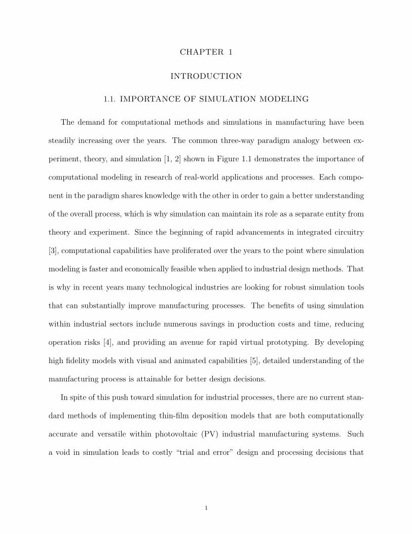
periment, theory, and simulation [1, 2] shown in Figure 1.1 demonstrates the importance of
computational modeling in research of real-world applications and processes. Each compo-
nent in the paradigm shares knowledge with the other in order to gain a better understanding
of the overall process, which is why simulation can maintain its role as a separate entity from
theory and experiment. Since the beginning of rapid advancements in integrated circuitry
[3], computational capabilities have proliferated over the years to the point where simulation
modeling is faster and economically feasible when applied to industrial design methods. That
is why in recent years many technological industries are looking for robust simulation tools
that can substantially improve manufacturing processes. The benefits of using simulation
within industrial sectors include numerous savings in production costs and time, reducing
operation risks [4], and providing an avenue for rapid virtual prototyping. By developing
high fidelity models with visual and animated capabilities [5], detailed understanding of the
manufacturing process is attainable for better design decisions.
In spite of this push toward simulation for industrial processes, there are no current stan-
dard methods of implementing thin-film deposition models that are both computationally
accurate and versatile within photovoltaic (PV) industrial manufacturing systems. Such
a void in simulation leads to costly “trial and error” design and processing decisions that
1
Theory
Simulation
Experiment
Figure 1.1. Analogy of the three-way process interaction between theory,experiment, and simulation
impede the progress toward optimal solutions in thin-film deposition, most notably the thin-
film uniformity across large PV modules. Furthermore, the absence of simulation prevents
further system design exploration since experiments are only limited to an understanding
of the current system capabilities rather than finding other alternatives to improve the PV
manufacturing process. Therefore developing a standard simulation method in the thin-film
and PV industries will help give a detailed understanding of the overall manufacturing pro-
cess that will lead to better design decisions. These accurate simulations can be applied to
various processing conditions without running the risk of compromising the current depo-
sition tool or its thin-film materials. Simulation modeling is also scalable and thus can be
expanded to both small and large-scale PV production lines that cannot be done as easily
with experiments alone. Inclusion of the simulation component in the research methodol-
ogy of thin-film deposition will ultimately save manufacturing time in optimizing thin-film
uniformity as well as costs and resources associated with the deposition process.
2
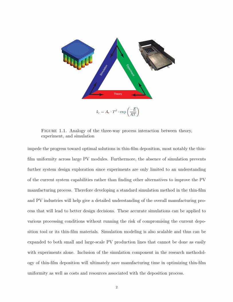
One example of the benefits seen locally within deposition modeling has been the inves-
tigation of Cadmium Sulfide (CdS) deposition during a processing technique known as Close
Space Sublimation (CSS) [6]. Transient simulations on Cd and S2 species diffusion through
the control volume of the CdS bottom source revealed pre-existing non-uniformities of sev-
eral percent across the deposition area using the original CdS source geometry. Switching to
a deeper pocket with more shallow wells led to a much more uniform deposition across the
same area (Figure 1.2) during CSS operation that was verified with experimental results.
Such results indicate the usefulness simulation modeling has on determining uniformities
within thin-film deposition techniques and how new predictive solutions can be extended
to other materials such as CuCl. The next section will provide background information on
CuCl and its function as a doping mechanism of the Cadmium Telluride (CdTe) absorber
layer. It will hopefully become evident as to why CuCl adsorption uniformity plays such a
vital role to the efficiency of CdTe solar cells made at CSU and how thin-film growth analysis
from both an experimental and computational standpoint can assist in understanding the
inherent mechanism of CuCl thin-film growth.
Figure 1.2. Original and modified CdS source contour plots demonstratingthe improved deposition rate uniformity across the substrate (image takenwith permission from [6])
3
1.2. BACKGROUND OF CuCl IN THIN-FILM PV APPLICATIONS
CuCl is classified as a semiconducting material that displays useful properties when ap-
plied to thin-film PV deposition and has been studied for many decades. Previous research
conducted on CuCl as an evaporant to form Cu2S on a CdS layer [7, 8] aided in a PV fab-
rication process that produced solar cell efficiencies of < 10%. However, dramatic efficiency
losses due to, at least in part, uncontrolled stoichiometric instabilities in the films [9] pre-
vented these PV materials from being competitive in the energy market. Over time, much
of the solar cell community continued to look for new arrangements and semiconducting ma-
terials to achieve higher efficiencies. To date, CuCl is primarily used as a dopant for various
thin-film PV devices, most notably CdTe. The device structure of a baseline CdTe PV device
shown in Figure 1.3a illustrates where CuCl is typically introduced in the fabrication process.
Here at CSU, CuCl is sublimated via CSS as a precursor state and is deposited onto the
CdTe absorber layer. After deposition, annealing takes place on the substrate, during which
Cu diffuses into the CdTe layer and forms shallow donor regions [10] that aid in the solar
cell efficiency. Figure 1.3b [11] depicts the J-V curves when CdTe is intentionally Cu-doped
vs an undoped cell. It is evident that the PV device with Cu included resembles a diode-like
behavior that results in higher efficiency while the cell with no Cu develops unfavorable kinks
in the curve. There is a limit to beneficial effects of Cu doping, however. It is well known
among the CdTe PV community that too much Cu doping can cause cell degradation that
affects the open-circuit voltage Voc in the cell and lowers device performance [12, 13].
1.3. IMPORTANCE OF THESIS WORK
In order to help achieve a highly uniform Cu doping process, an overall understanding of
CuCl deposition in CSS must be developed. Such a task presents quite a number of challenges
4
Substrate/TCO
CdS Window Layer
CdTe Absorber
Layer
Nickel Paint
Cu-Doped CdTe Region
Carbon Paint
(a) (b)
Figure 1.3. (a) Typical CdTe device structure made in current CSS process(red layer marks the Cu-doped region in CdTe). (b) J-V curves of intentionallyCu-doped vs. undoped CdTe cell devices (image taken with permission from[11])
for many areas related to continuum-based simulation modeling and experimentation. In
order to begin simulating the deposition environment, a keen understanding of the theory
involved within CSS needs to be established so that connections can be made between system
parameters and how they affect both sublimation and adsorption of CuCl. After this initial
step, a thin-film growth model can be built that encompasses such kinetic processes across
a wide range of system parameters. The collection of CuCl material properties as a function
of such parameters is accomplished as well. The simulation model finally requires some
type of experimental verification of its computational accuracy. If the model does not fully
represent the experimental results with a high degree of accuracy, then refinement of the
modeling setup must be done. Refinement may be repeated many times before a well-
behaved solution is obtained that can accurately predict thin-film deposition conditions. The
research presented here follows this multistep process in regards to CuCl thin-film growth
5
on Fluorine-doped Tin Oxide (FTO), or “Transparent Conductive Oxide” (TCO), coated
substrates (both terms are used interchangeably throughout this work). Equally important
in this study is the characterization of the CuCl thin-films, which elucidates some key growth
mode characteristics exhibited by CuCl during CSS. It is hoped that the efforts made in this
work can eventually assist in controlling the amount of CuCl adsorbing to the CdTe layer
and potentially lead to a more uniform back contact that can maintain higher CdTe PV
efficiencies.
6
CHAPTER 2
THEORY
The physical phenomena associated with CSS can be separated into two underlying
processes: 1) sublimation of a particular bulk species (i.e. CuCl) within the pocket domain,
and 2) adsorption of the resulting vapor species on a substrate layer. Numerous factors such
as pressure, temperature, and surface preparation influence the kinetic rates of both processes
and add much complexity to the resulting growth overlayers. Furthermore, several kinetic
processes [14] involved with thin-film growth (many of which are beyond the scope of this
work) are governed by probabilistic interactions that require ab initio molecular dynamics
[15] to fully comprehend. This chapter simply focuses on distinguishing the characteristics of
sublimation and adsorption from a theoretical perspective while considering other important
terms that correct for the deviation found in actual thin-film growth rates. The chapter will
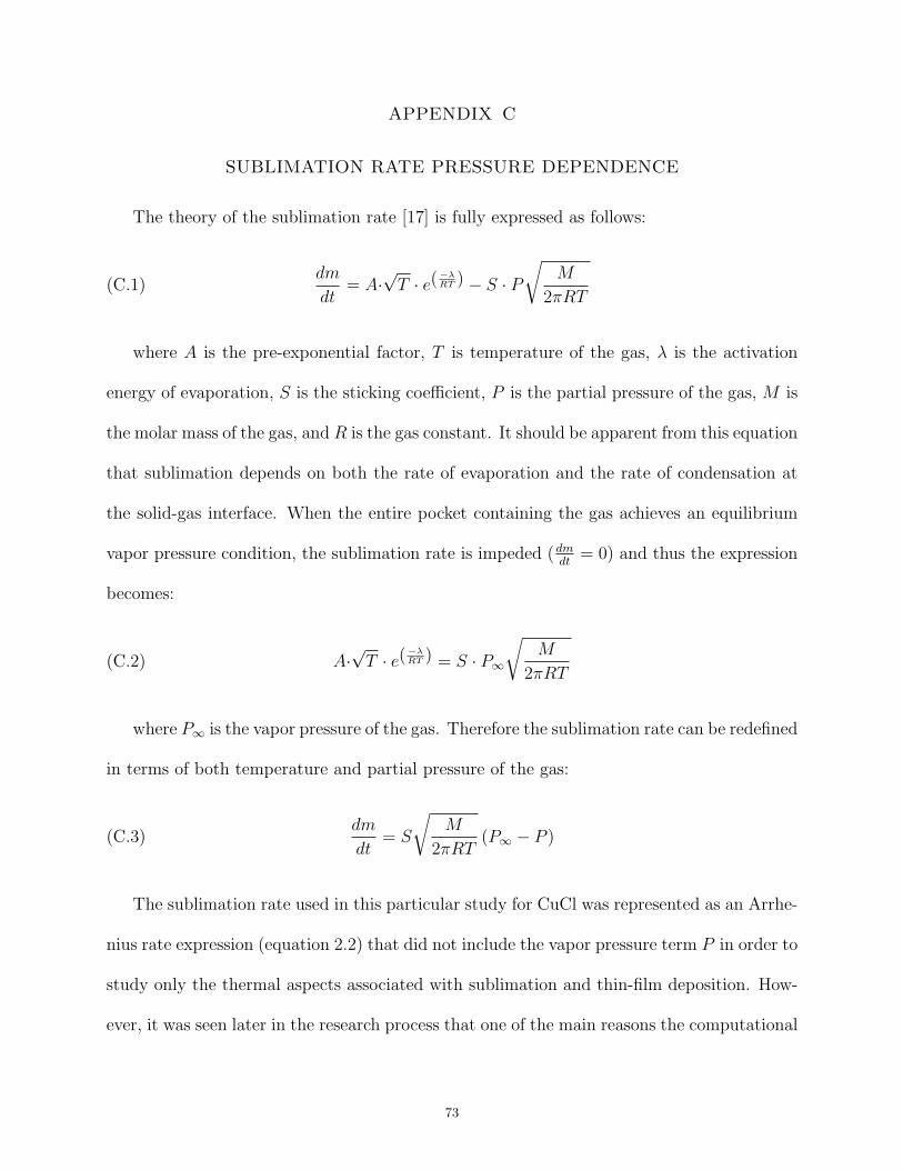
In equation 2.2, A is the pre-exponential factor, E denotes the activation energy, T
is temperature of the source [K], and R is the universal gas constant [8314 J/kgmol-K].
Although not explicitly stated in equation 2.2, sublimation can be influenced by pressures in
the system that span the diffusion-limited regime (⇡ > 50 mTorr) [16]. However, the normal
operating pressure within the CSS deposition system is at 40 mTorr, which is less than the
diffusion-limited case. Furthermore, the controlled flow of ambient mixed-gas (98% N2, 2%
O2) is maintained at this pressure throughout the entire system operation. Therefore it was
assumed that the sublimation rate obtained from this particular study was independent of
operating pressure and thus only varied with source temperature. This was done to focus
solely on an investigation of the thermal aspects of the system rather than coupling it with
operating pressure dependencies.
Figures 2.1a - 2.1d provide schematics of CuCl sublimation within the CSS chamber as
the CuCl partial pressure increases to saturation within the source pocket geometry at a
given source temperature Tsource. Sublimation begins with a few CuCl molecules having
enough thermal energy to break their solids bonds to become vapor (Figure 2.1a). Over
time, a CuCl partial pressure continues to build within the pocket since the evaporation rate
is greater than the condensation rate at the solid-gas interface (Figure 2.1b). At saturation
(Figure 2.1c), equilibrium vapor pressure of CuCl is achieved since the evaporation rate is
now equal to the condensation rate (Figure 2.1d). Therefore no further sublimation occurs
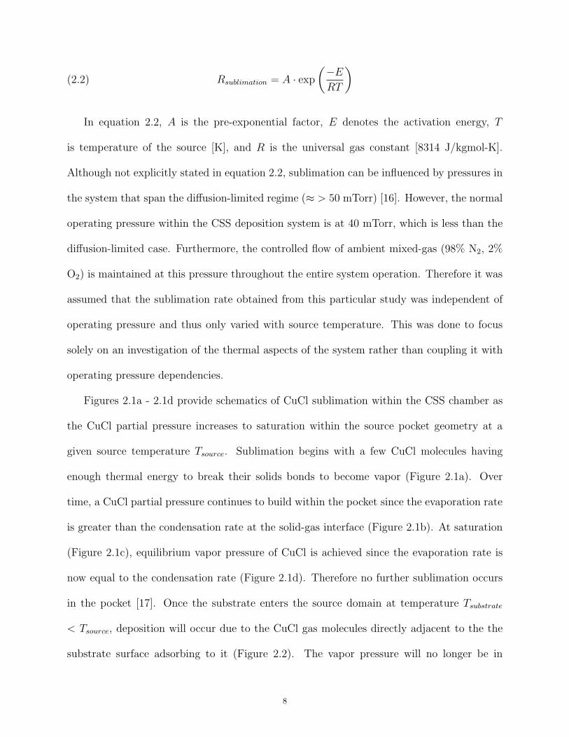
in the pocket [17]. Once the substrate enters the source domain at temperature Tsubstrate
< Tsource, deposition will occur due to the CuCl gas molecules directly adjacent to the the
substrate surface adsorbing to it (Figure 2.2). The vapor pressure will no longer be in
8
Graphite
Bottom Source
Graphite
Top Heater
Shutter
(a) (b)
(c)
: Cu
: Cl
(d)
Figure 2.1. CuCl sublimation within the bottom source. CuCl partial pres-sure eventually reaches saturation as long as the surface temperatures withinthe pocket are equal and no leaks are present while the shutter is coveringthe source pocket. (d) is a zoomed representation of one of the bottom sourcewells from (c) when the evaporation rate is equal to the condensation rate atthe solid-vapor interface.
equilibrium and thus sublimation is driven until the source sublimation rate, along with the
deposition rate on the surface, again reaches equilibrium vapor pressure.
9
2.1.2. ADSORPTION. When the shutter is removed and the end-effector along with a
substrate slides over the CuCl pocket, a thermal gradient is formed throughout the gaseous
species (Figure 2.2). This is due to the substrate temperature Tsubstrate being less than the
temperature of the CuCl gas species monolayer directly adjacent to the substrate. The colder
substrate surface acts as a thermal energy sink for these CuCl gas molecules, causing them to
preferentially move toward it. As the CuCl vapor impinges on the surface, the gas molecule
may lose enough kinetic energy during collision with the substrate in order to adhere to it,
resulting in a process known as adsorption. Adsorption can either be a physical process
that relies on Van Der Waals forces to hold the adsorbate gas species to the adsorbent bulk
layer (a.k.a. physisorption) or a chemically activated process that combines both species
with strong chemical bonds (a.k.a. chemisorption). The latter case creates a much stronger
force and thus requires more energy to cause the gas molecule to desorb from the bulk layer.
However, in this study physisorption is the dominant adsorption mechanism for CuCl on the
FTO-coated substrate.
In order to fully understand how the adsorption rate is calculated, the rate of impingement
by a gas on a particular surface must be determined. According to kinetic theory, the
impingement rate is the amount of incoming molecules per second that hit a surface within
a given area [18] and is expressed as follows:
(2.3) Φ =Pp
2⇡MRT
where P = partial pressure of gas species impinging on the surface, M = gas species
tends to reformulate the impingement rate in terms of species concentration as oppose to
10
: Cu
Graphite
Bottom Source (Tsource
)
Graphite
Top Heater
: Cl
Substrate (Tsubstrate
)
Tsubstrate
< Tsource
Figure 2.2. CuCl adsorption occurring at the substrate. Adsorption is dic-tated by a sticking coefficient on a given surface that can be attributed to oneof the three systematic growth mechanisms.
partial pressure. Therefore equation 2.3 can be rewritten as:
(2.4) Φ = CCuClg
r
RT
2⇡M
where CCuClg is the CuCl molar concentration [kmol/m3]. The impingement rate can be
thought of as all incoming vapor molecules sticking to a surface. In reality, adsorption rates
are typically much less than Φ due to imperfect surface conditions, preferred orientation,
surface temperature, and ambient pressures. An overall representation of these complex
limiting factors is known as the sticking coefficient S. This accommodating factor in its
simplest form is written as:
(2.5) S =Radsorption
Φ
11
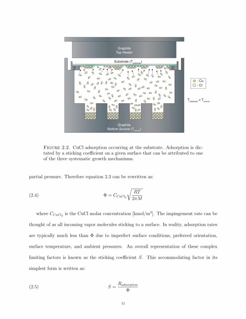
As depicted in Figure 2.3, an impingement flux of CuCl gas occurs at some initial time
t0, after which some ∆t time passes, two possibilities are given: 1) all molecules impinging
on the substrate stick to it (S = 1), or 2) some molecules do not stick and are reflected
back into the vapor species (S < 1). In most real-world cases, S is a value between 0
and 1. Since the sticking coefficient is associated with many varying conditions of a given
system, it is difficult to obtain a general solution for S that encompasses a wide range of
systematic processes. Nonetheless, its contribution to the adsorption rate is a key aspect in
thin-film growth analysis. Within this research work the sticking coefficient is attempted to
be generalized for a certain CuCl temperature regime and process condition. Calculating S
as a function of temperature may lead to a quantifiable model of the CuCl adsorption rate,
but a brief look at the types of possible growth mechanisms in thin-films will help assess
what type of growth behavior CuCl exhibits.
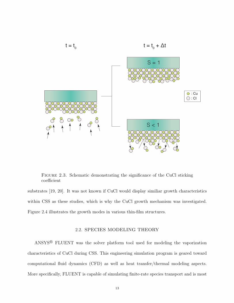
2.1.3. GROWTH MECHANISMS. Three growth mechanisms are used to classify the
growth behaviors of thin-films according to the type of substrate and overlayer used during
deposition: i) Volmer-Weber, ii) Frank-Van der Merwe, and iii) Stranski-Krastanov. Volmer-
Weber growth occurs when clusters of the condensed species form islands on the substrate
rather than a uniform layer. This is primarily due to the condensed species having a higher
surface energy than the substrate to which it is adhering, making it more energetically
favorable for island formation to occur. On the other hand, Frank-Van der Merwe is a layer-
by-layer deposition phenomena in which the surface energy of the substrate is greater than the
energy required to cluster the atoms together. The final mode known as Stranski-Krastanov
growth is a combination of layered growth for the first few monolayers upon reaching a critical
thickness where island growth becomes more favorable [18]. Previous studies have shown
that the Stranski-Krastanov mode is prominent during CuCl heteroepitaxial growth on MgO
12
: Cu
: Cl
t = t0
t = t0 + Δt
S = 1
S < 1
Figure 2.3. Schematic demonstrating the significance of the CuCl stickingcoefficient
substrates [19, 20]. It was not known if CuCl would display similiar growth characteristics
within CSS as these studies, which is why the CuCl growth mechanism was investigated.
Figure 2.4 illustrates the growth modes in various thin-film structures.
characteristics of CuCl during CSS. This engineering simulation program is geared toward
computational fluid dynamics (CFD) as well as heat transfer/thermal modeling aspects.
More specifically, FLUENT is capable of simulating finite-rate species transport and is most
13
Volmer-Weber Frank Van der Merwe Stranski-Krastanov
t 0t 0
+ ∆
tt 0
+ 2∆
t
Figure 2.4. Primary growth modes displayed by various thin-films. Suchmodes are dependent on the surface energies of the substrate and adsorbedoverlayer
applicable to this research work. For all simulations the species transport algorithm was en-
abled for describing the CuCl volumetric and wall-adhering species governed by the following
equation:
(2.6)@(⇢Yi)
@t+r · (⇢~uYi) = −r · (~Ji) +Ri + Si
where ⇢ = density, ~u = momentum vector, Yi = local mass fraction, ~Ji = diffusion flux,
Ri = net rate production, and Si = source term of species i [21]. The first term on the
left-hand side of the equation is the rate of change of the species mass fraction while the
second term is related to convection. On the right-hand side, the first term is the divergence
of the diffusion flux, the second term is the rate of production of the gas species i, and the
third term an additional species source expression. Since the CuCl simulation was defined to
be a steady-state problem with negligible convection effects and no additional source terms,
14
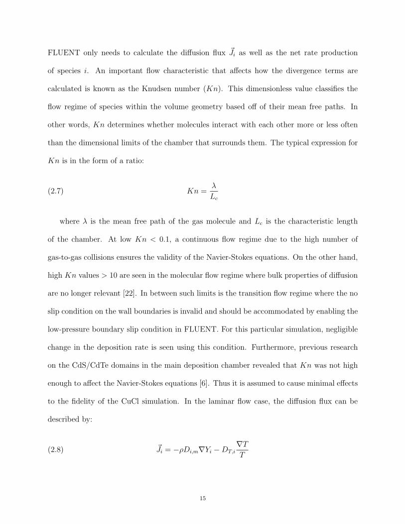
FLUENT only needs to calculate the diffusion flux ~Ji as well as the net rate production
of species i. An important flow characteristic that affects how the divergence terms are
calculated is known as the Knudsen number (Kn). This dimensionless value classifies the
flow regime of species within the volume geometry based off of their mean free paths. In
other words, Kn determines whether molecules interact with each other more or less often
than the dimensional limits of the chamber that surrounds them. The typical expression for
Kn is in the form of a ratio:
(2.7) Kn =λ
Lc
where λ is the mean free path of the gas molecule and Lc is the characteristic length
of the chamber. At low Kn < 0.1, a continuous flow regime due to the high number of
gas-to-gas collisions ensures the validity of the Navier-Stokes equations. On the other hand,
high Kn values > 10 are seen in the molecular flow regime where bulk properties of diffusion
are no longer relevant [22]. In between such limits is the transition flow regime where the no
slip condition on the wall boundaries is invalid and should be accommodated by enabling the
low-pressure boundary slip condition in FLUENT. For this particular simulation, negligible
change in the deposition rate is seen using this condition. Furthermore, previous research
on the CdS/CdTe domains in the main deposition chamber revealed that Kn was not high
enough to affect the Navier-Stokes equations [6]. Thus it is assumed to cause minimal effects
to the fidelity of the CuCl simulation. In the laminar flow case, the diffusion flux can be
described by:
(2.8) ~Ji = −⇢Di,mrYi −DT,irT
T
15
whereDi,m = mass diffusion coefficient andDT,i = thermal diffusion coefficient for species
i. It is evident from equation 2.8 that the diffusion flux is dictated by both the concentration
and thermal gradient across the CuCl vapor species and will consequently determine the
deposition rate possible on a specified wall surface. Both the mass and thermal diffusion
coefficients Di,m and DT,i were calculated using the available kinetic theory option under
mixture materials. Two inputs known as the Lennard-Jones (L-J) parameters were necessary
for solving any material properties governed by kinetic theory. The L-J characteristic length
σ is described as the equilibrium distance between two given atoms during which zero net
energy (i.e. repulsive energy - attractive energy = 0) is acting on them. The energy parameter
✏/kb is attributed to the minimum potential energy well (i.e. highest attractive energy)
between two atoms that induce dipole moments in each other [23]. There are no readily
available L-J parameters for CuCl within research literature, thus a simple calculation using
data obtained from Monte Carlo simulations on Cu [24] and Cl [25] was performed via the
Berthelot Mixing Rule:
σab =σaa + σbb
2(2.9)
✏ab =p✏aa✏bb(2.10)
where a and b refer to Cu and Cl, respectively. The calculated parameters for CuCl were
σ = 2.789 A and ✏ = 914.087 K.
The Pressure-Based Coupled Solver used in this simulation initially solves for the mass
and momentum equations, which is followed by the energy equation for each iteration. Such
equations will compute the main domain properties such as temperature, density, enthalpy,
velocity components, and pressure at each cell-center of the mesh. Thereafter equation 2.6
16
is calculated along with the aforementioned properties per iteration until their residuals con-
verge to a steady-state condition. The final solution provides Yi cell-center values necessary
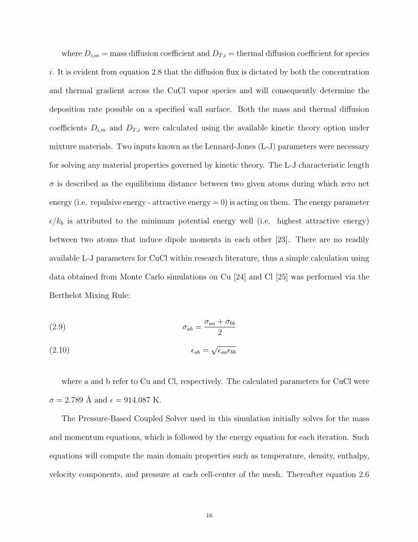
to describe the CuCl concentration gradient throughout the pocket (Figures 2.5a and 2.5b).
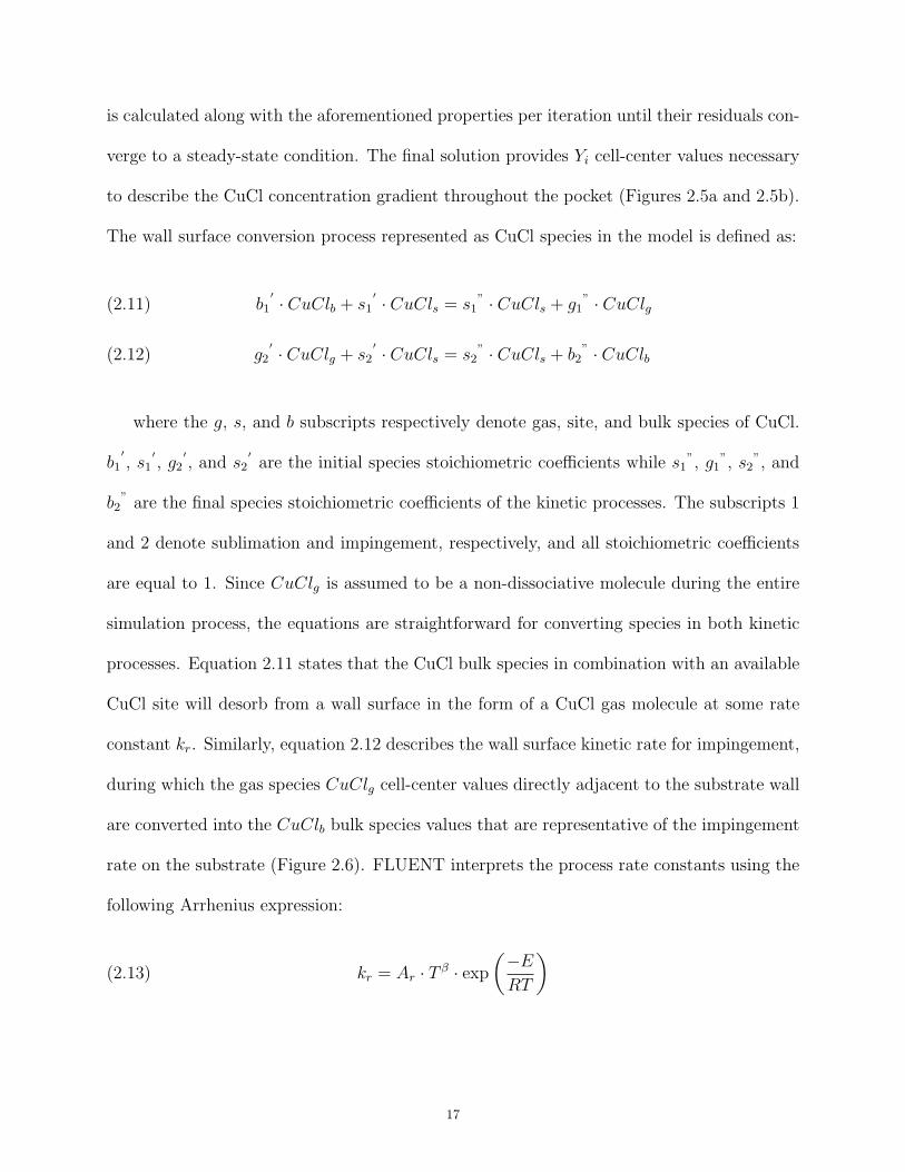
The wall surface conversion process represented as CuCl species in the model is defined as:
b10 · CuClb + s1
0 · CuCls = s1” · CuCls + g1
” · CuClg(2.11)
g20 · CuClg + s2
0 · CuCls = s2” · CuCls + b2
” · CuClb(2.12)
where the g, s, and b subscripts respectively denote gas, site, and bulk species of CuCl.
b10
, s10
, g20
, and s20
are the initial species stoichiometric coefficients while s1”, g1
”, s2”, and
b2” are the final species stoichiometric coefficients of the kinetic processes. The subscripts 1
and 2 denote sublimation and impingement, respectively, and all stoichiometric coefficients
are equal to 1. Since CuClg is assumed to be a non-dissociative molecule during the entire
simulation process, the equations are straightforward for converting species in both kinetic
processes. Equation 2.11 states that the CuCl bulk species in combination with an available
CuCl site will desorb from a wall surface in the form of a CuCl gas molecule at some rate
constant kr. Similarly, equation 2.12 describes the wall surface kinetic rate for impingement,
during which the gas species CuClg cell-center values directly adjacent to the substrate wall
are converted into the CuClb bulk species values that are representative of the impingement
rate on the substrate (Figure 2.6). FLUENT interprets the process rate constants using the
following Arrhenius expression:
(2.13) kr = Ar · T β · exp✓
−E
RT
◆
17
= Wall Boundary Face-Center
= Gas Species Cell-Center (Unsolved)
= Impingement Face-Center
= Gas Species Cell-Center (Solved)
= Sublimation Face-Center
(a)
(b)
Figure 2.5. Schematic of species transport calculation throughout entiremesh domain. (a) Sublimation kinetic rate is enabled to allow FLUENTto compute and store the mass fraction Y for CuCl in the cell-centers thatare compared to surrounding values that determine whether a solution forr~Ji = Ri has converged. (c) After convergence, the 1st adjacent cell-centerlayer to the substrate impingement face-centers will influence the impingementrate calculated to obtain a simulated CuCl thickness.
It should be evident that equation 2.13 is a modified form of equation 2.2 with an ad-
ditional temperature term raised to some β constant. Furthermore, the kr rate constant
can be simplified to match the form of impingement rate equation 2.4. Setting r = 1 for
18
Figure 2.6. Example of CuCl mass fraction calculated in simulation modelbased off of R1 (sublimation) at the bottom source and R2 (impingement) atthe substrate
sublimation and r = 2 for impingement, the final kinetic rates R1 and R2 may be expressed
as follows:
R1 = −A1 · exp✓
−E
RTsource
◆
+B1 · CCuClg − C1(2.14)
R2 = A2 · CCuClg
p
Tsubstrate(2.15)
where A1 and A2 can be derived from calculating the constant terms in equations 2.2
and 2.4 respectively. B1 and C1 were included in equation 2.2 to provide additional function-
ality to the sublimation rate with respect to CuCl partial pressure if necessary. By activating
these kinetic mechanisms on particular wall surfaces as well as applying the stoichiometric
coefficients from equations 2.11 and 2.12, a net molar rate of production or consumption
[kg-mol/m2-s] on a particular wall of the mesh domain can be calculated to determine the
19
gas, site, and bulk CuCl species. Equations 2.16 - 2.18 define these calculations for each
respective term:
Rg =⇣
g1” − g1
0
⌘
·R1(2.16)
Rs = 0(2.17)
Rb =⇣
b2” − b2
0
⌘
·R2(2.18)
where g1” and b1
” = 1 and g10
and b10
= 0. It should be noted that Rs = 0 means that
the CuCl site species is constant throughout the entire wall surface adsorption process. A
reaction-diffusion balance is made at the wall during each iteration until steady-state con-
vergence is achieved, during which the mass deposition rate on the wall surface is calculated:
(2.19) mdep = M · Rb
Again, M = CuCl molar mass [kg/kg-mol]. Converting the units of mdep from [kg/m2-s]
to [nm/s] will ultimately lead to the simulated impingement rate Φ as shown by equation 2.20:
(2.20) Φ =mdep · 109
⇢
Multiplying the impingement rate Φ by the deposition time t provided a simulation
thickness at each particular substrate and source temperature for further comparison to
experimental thicknesses, which will be described in the next chapter.
20
CHAPTER 3
EXPERIMENTAL/SIMULATION METHODS
The experiments performed within this research were focused on quantifying both the
sublimation and adsorption rates of CuCl during the CSS process. Since the simulation of
CuCl thin-film growth rates required an accurate representation of sublimation within the
CSS apparatus, CuCl mass-loss measurements were recorded and used for further sublimation
rate calculations. This chapter will explain the method of measuring the CuCl sublimation
also elaborate on the multi-step technique developed to measure the CuCl thickness across
the substrate at pre-determined locations. Finally a description of the mesh model, along
with its boundary conditions obtained from theoretical aspects defined in Chapter 2, will
be elaborated for CuCl thickness simulations. This chapter aims to bridge the gap between
CuCl experimental and simulated growth rate results.
3.1. CSS TECHNIQUE IN CuCl THIN-FILM GROWTH
CuCl growth rates were varied by sweeping a range of thermal parameters for each
deposition run using the Advanced Research Deposition System (ARDS). This versatile tool
contains several CSS stations, each equipped with a graphite top heater and bottom heating
source where the material powder, in this case CuCl, is sublimated. Both the top heater and
bottom source temperatures are adjusted by electrically heating the Nickel-Chromium coil
embedded in each graphite fixture and maintained via PID control. The heaters were kept
at near steady-state conditions since temperature fluctuations (top heater: 1-2◦C, bottom
source: < 1◦C) occurred due to the PID control setup. Approximately 63.9 SCCM of mixed
gas (98% N2, 2% O2) is flown throughout the chamber while maintaining an ambient pressure
21
of 40 mTorr using a Leybold D65 rotary vane mechanical pump and a Varian VHS-4 diffusion
pump.
Pilkington TEC-12D glass substrates (78 x 90 mm2) were used during each deposition
run and were ordered with a TCO pre-layer consisting of FTO covering one side of the glass.
The substrates were initially rinsed, sonicated, and N2 dried [11] to keep surface conditions
as clean as possible. All substrates were plasma-cleaned in a 200 mTorr N2 environment for
30 s before entering the main chamber. Initial CuCl experiments were performed at normal
process of recipe (POR) conditions, which pertain to heating the substrate to > 400◦C prior
to thin-film deposition and depositing CuCl on the substrate for 110 s. However, thicknesses
of the resulting CuCl thin-films were too inconsistent to be measured with any available
instruments. Therefore, it was decided that all substrates were to directly enter the CuCl
domain without pre-heating and deposit for one hour to obtain easily measurable CuCl
thin-films as well as reach steady-state equilibrium conditions within the domain. As a
result, CuCl films were produced with a thickness that could be measured consistently and
accurately.
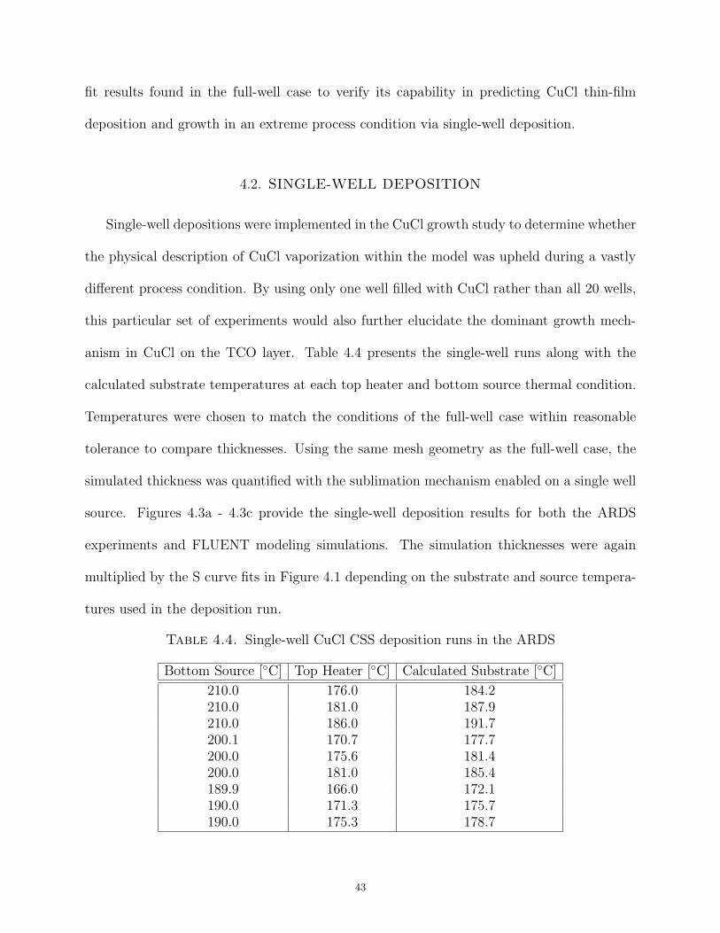
Two sets of experiments were ran in the ARDS: 1) full-well and 2) single-well deposition.
Full-well deposition refers to all 20 wells in the graphite bottom source being 1/2 filled
with CuCl powder, which is the typical POR setup for all sublimation sources. As the name
implies, single-well deposition only used one well 1/2 filled with CuCl while leaving the other
19 source wells empty. Simulation models for both cases were also developed and compared
to the experiments. The full-well deposition case was used to check the initial accuracy of
the impingement rate obtained from the simulation and compare it to the actual adsorption
rate given by experimental data. A sticking coefficient curve fit for each substrate and source
temperature could then be obtained for later use with the single-well deposition model. The
22
full-well runs were also used to determine the growth mode exhibited by CuCl on the FTO
layer via characterization analysis. The main goal for using the single-well deposition case
was to verify the model’s accuracy in describing the physical processes associated with CSS
during an extreme processing condition. Actual images of the full and single-well CuCl
setups can be found in Figures 3.1a and 3.1b.
(a) (b)
Figure 3.1. (a) Full-well and (b) single-well depositions in the ARDS. Uponfurther analysis, the distinct color difference between experiments indicatedwhether the CuCl powder continuously sublimated (darker) or not (lighter)after completing all deposition runs.
Top heater and bottom source temperatures were systematically varied per substrate. It
was necessary to determine the substrate temperature during each deposition run. However
the Mikron-MI-N5/5+ series pyrometer installed at the CuCl chamber entry was unable to
properly measure the substrate temperatures, either due to calibration error in emissivity,
pyrometer positioning, or a combination of both. It was decided that substrate temperatures
were to be calculated using a simplified radiation heat transfer expression dependent on the
23
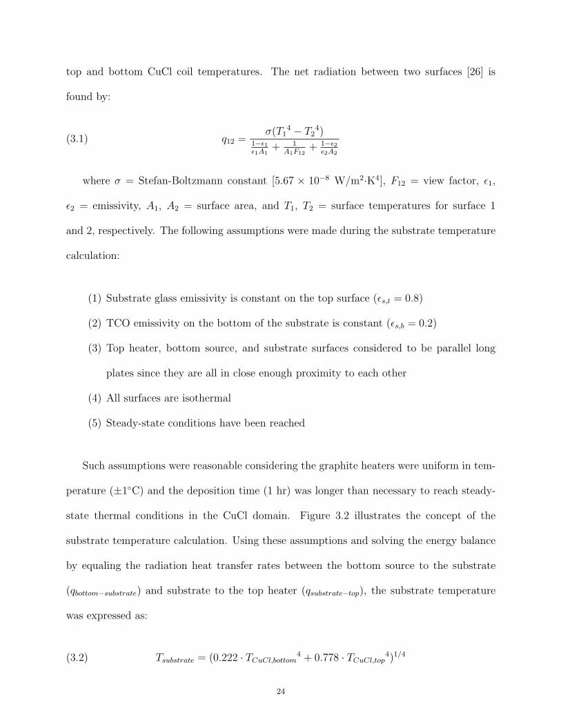
top and bottom CuCl coil temperatures. The net radiation between two surfaces [26] is
Figure 3.2. Illustration of the substrate temperature calculation
where TCuCl,bottom and TCuCl,top were the respective bottom and top CuCl heater temper-
atures. All substrate depositions (full and single-well) were classified by their substrate and
source temperatures as recorded in Tables 4.1 and 4.4 found in Chapter 4.
3.2. CuCl MASS-LOSS EXPERIMENT
Studies on CuCl vapor pressure [7, 27–29] during sublimation were analyzed to see if their
vapor pressure curves embodied the standard kinetic rates found in the ARDS operation
regime. However, CuCl sublimation rates at temperatures < 300◦C were not well defined in
previous literature and most studies performed experiments at different baseline pressures
than the typical ARDS operating pressure (40 mTorr). Larger molecular vapor species such
as Cu3Cl3 trimers are more prevalent at higher temperatures than the expected CuCl vapor
[7], further deviating from CSS conditions. It was not known if such sublimation rates
were representative of that seen in CSS and was therefore imperative to obtain an empirical
expression for the CuCl sublimation rate within the ARDS. This would ensure the data
25
used to calculate the sublimation rate were within the applicable temperature and pressure
regimes and could be applied to the simulation model.
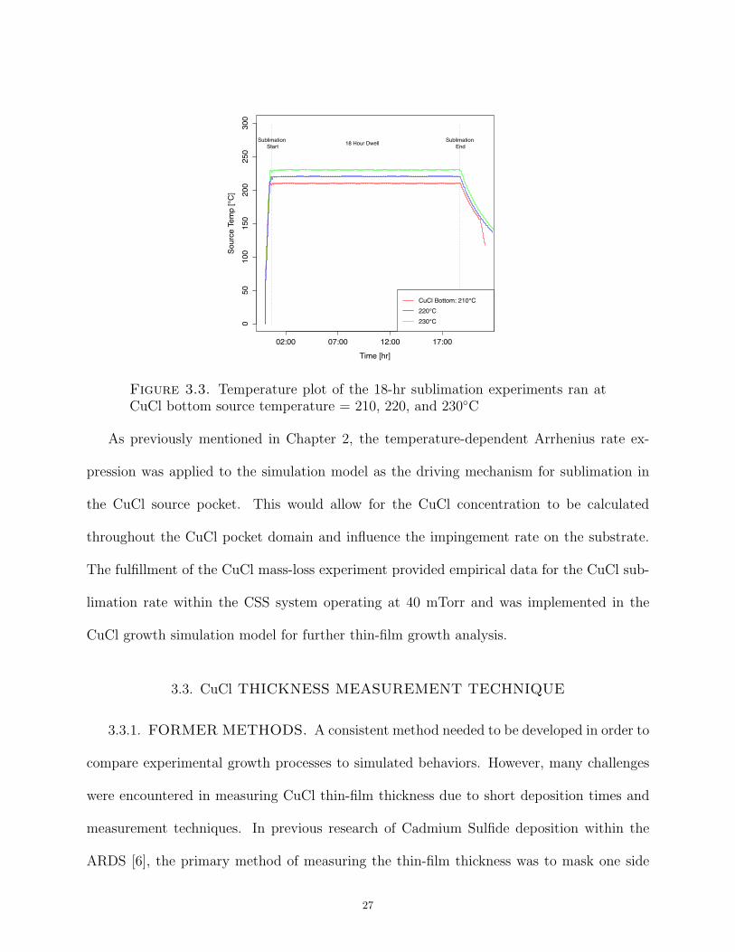
The CuCl mass-loss experiment was performed in the ARDS CuCl bottom source using
four graphite crucibles machined to fit in the source wells. Each crucible was weighed five
times before and after sublimating using a Mettler AE163 mass balance. The crucibles were
filled with 1/4 tsp of CuCl powder and baked for approximately 18 hours to minimize the
amount of water vapor accumulation in the materials and replicate typical CuCl powder
conditions after an extended period of usage. The crucibles were sublimated at 210, 220,
and 230◦C for 18 hours at each temperature to ensure steady-state sublimation. Previous
experiments revealed prolonged exposure to ambient conditions noticeably affected mass
measurements. It is believed that water vapor was the main culprit to this detrimental
factor. Each experiment run was performed immediately after measuring CuCl mass to
prevent the crucibles and/or CuCl powder from collecting water vapor and resulting in
misleading mass analyses. Temperature logs were recorded for the bottom source within the
CuCl domain to determine whether thermal equilibrium was sustained throughout the entire
sublimation process (Figure 3.3). After calculating the CuCl mass-loss at each particular
source temperature and crucible, a log curve fit was applied to the entire data set to define
the sublimation rate as an Antoine expression shown in equation 2.1:
(3.3) log(Rsublimation) =−6503.8
T+ 4.8741
The Arrhenius rate expression derived from equation 3.3 is provided:
(3.4) Rsublimation = 74831.93 · exp✓
-1.2451e8
RT
◆
[kg-mol/m2 · s]
26
02:00 07:00 12:00 17:00
05
01
00
15
02
00
25
03
00
Time [hr]
So
urc
e T
em
p [
°C]
CuCl Bottom: 210°C
220°C
230°C
18 Hour DwellSublimation
End
Sublimation
Start
Figure 3.3. Temperature plot of the 18-hr sublimation experiments ran atCuCl bottom source temperature = 210, 220, and 230◦C
As previously mentioned in Chapter 2, the temperature-dependent Arrhenius rate ex-
pression was applied to the simulation model as the driving mechanism for sublimation in
the CuCl source pocket. This would allow for the CuCl concentration to be calculated
throughout the CuCl pocket domain and influence the impingement rate on the substrate.
The fulfillment of the CuCl mass-loss experiment provided empirical data for the CuCl sub-
limation rate within the CSS system operating at 40 mTorr and was implemented in the
CuCl growth simulation model for further thin-film growth analysis.
3.3. CuCl THICKNESS MEASUREMENT TECHNIQUE
3.3.1. FORMER METHODS. A consistent method needed to be developed in order to
compare experimental growth processes to simulated behaviors. However, many challenges
were encountered in measuring CuCl thin-film thickness due to short deposition times and
measurement techniques. In previous research of Cadmium Sulfide deposition within the
ARDS [6], the primary method of measuring the thin-film thickness was to mask one side
27
of the diagonal of the substrate with etchant tape and etch away the unmasked side with
Hydrochloric Acid (HCl). Doing so created a step height between the now bare TCO layer
and the CdS overlayer that was measured across the entire substrate diagonal. Similar
attempts were made to measure the CuCl thicknesses using this method while depositing
CuCl near POR conditions (110 s). But since CuCl was much thinner than CdS at POR,
etching one side of the CuCl layer would unexpectedly roughen the TCO below and lead to
misleading thickness results.
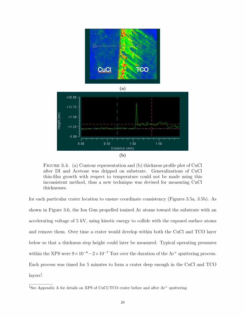
The next attempt included dripping one or a combination of the three solutions, Iso-
propanol (IPA), de-ionized water (DI), or Acetone, on the CuCl layer to create craters as
the measured step heights. CuCl deposition was again done for 110 seconds. Unfortunately
the craters formed by either solution migrated CuCl to their outer perimeters and caused
erroneous delta steps that were not representative of the thickness as shown in Figures 3.4a
and 3.4b. The same effect occurred when substrates were dipped in either IPA or DI. Fur-
thermore, the 110 s CuCl depositions had very little CuCl on the substrates (< 5 nm),
making measurements unfeasible with the available instruments.
3.3.2. CURRENT METHOD. A new multi-step method was implemented to measure
the CuCl thicknesses accurately and consistently. The method is summarized into three sub-
sequent steps: 1) Argon Ion Beam sputtering to form a crater deep enough into both the
CuCl and TCO layers, 2) measuring the crater depth using scanning white light interferom-
etry (SWLI), and 3) etching CuCl overlayer with HCl and remeasuring the crater depth to
determine the overall step height difference.
3.3.2.1. Argon Ion Beam Sputtering. The Argon Ion Beam in the X-ray Photoelectron
Spectroscopy (XPS) instrument was utilized to create 10 craters shaped like a rounded
rectangle across the diagonal of each substrate. Micrometer dial positions were determined
28
(a)
(b)
Figure 3.4. (a) Contour representation and (b) thickness profile plot of CuClafter DI and Acetone was dripped on substrate. Generalizations of CuClthin-film growth with respect to temperature could not be made using thisinconsistent method, thus a new technique was devised for measuring CuClthicknesses.
for each particular crater location to ensure coordinate consistency (Figures 3.5a, 3.5b). As
shown in Figure 3.6, the Ion Gun propelled ionized Ar atoms toward the substrate with an
accelerating voltage of 5 kV, using kinetic energy to collide with the exposed surface atoms
and remove them. Over time a crater would develop within both the CuCl and TCO layer
below so that a thickness step height could later be measured. Typical operating pressures
within the XPS were 9⇥10−8−2⇥10−7 Torr over the duration of the Ar+ sputtering process.
Each process was timed for 5 minutes to form a crater deep enough in the CuCl and TCO
layers1.
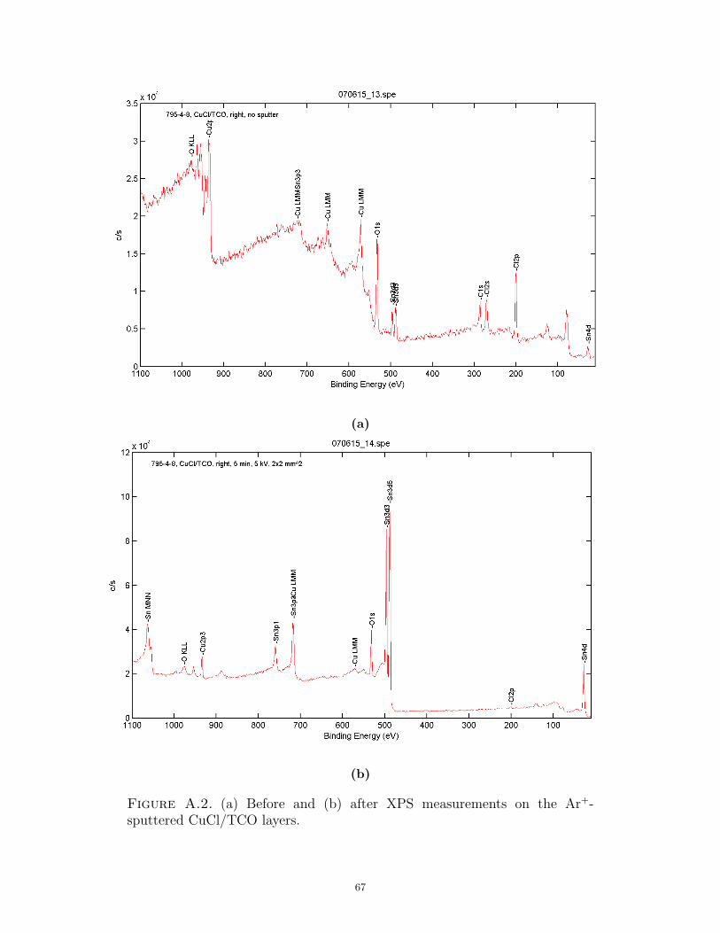
1See Appendix A for details on XPS of CuCl/TCO crater before and after Ar+ sputtering
29
(a) (b)
Figure 3.5. (a) Expected CuCl crater locations and (b) typical crater loca-tions on a TEC-12D substrate. The substrate is divided into 3 x 3 samplesthat are labeled by position values 1-9. Only positions 3, 5, and 7 are used forcrater etching
Argon Ion
Beam
CuCl
TEC-12D
Glass
TCO
Figure 3.6. Schematic of CuCl/TCO crater formation during Ar+ sputteringprocess
30
3.3.2.2. Scanning White Light Interferometry. The NewView 7300 instrument used for
measuring the CuCl thicknesses is known as a Scanning White Light Interferometer (SWLI).
This tool implements a nondestructive technique known as Coherence Scanning Interferom-
etry [30] that evaluates the metrology of a sample using a broadband spectrum (white light)
traveling toward the surface and reflects off of it, producing interference fringes at a cer-
tain scan height. The instrument vertically scans the entire topology along its optical axis,
obtaining contrast fringes throughout the entire scanning process. Frames at each height
variation are acquired successively by a 640⇥480 pixel CCD camera and processed into an
areal (3-D) representation of the surface (Figure 3.7a). For each small sample (26 x 30 mm2)
SWLI measured the crater depth before etching the CuCl thin-film with HCl. After the
first measurement, the CuCl layer was removed with HCl and cleaned with DI and IPA to
eliminate etchant residue and marks. A second measurement was performed on the etched
samples to determine the remaining TCO crater depth. The difference between the first and
second depth measurements resulted in a CuCl thickness at the crater location.
For all measurements, a gaussian spline low-pass filter with a filter high wavelength of
0.08 mm was included to reduce the surface noise due to CuCl roughness (3-5 nm) and
establish a CuCl thickness measurement closer to the average step height difference. The
instrument scanning distance was set at 40 µm to capture the entire topology on the substrate
surface. As shown in Figure 3.7b, a reference and test mask were created as the crater depth
displacement planes and all measurements were recorded using the evaluated peak-to-valley
mean values. For the reference mask areas (longer rectangular areas), a best fit cylinder form
was applied to remove the curvature within each sample due to thermal warping while in the
ARDS chamber. As a result, the mean top plane was analyzed in place of the curved surface
plane. Within the test mask (large square area) a high clipping parameter was specified to
31
(a)
Reference
Mask
Test Mask
Reference
Test
(b)
Figure 3.7. (a) Areal representation of a typical CuCl crater measured withSWLI. (b) Test and reference mask used within CuCl crater depth analysis,where the test mask is the entire area shaded in orange (purple) and thereference masks are the long rectangular boxes used as leveling planes for eachdata set.
remove any data > 2 nm above the deepest part of the crater. The average of the remaining
several thousand data points within the deepest crater area was used to measure the mean
CuCl step height to the top reference plane. The measurement process at each crater location
was repeated across the substrate diagonal and compared to the CuCl thickness simulation
results.
3.4. SIMULATION METHOD
The CuCl thin-film growth simulation model required an extensive study on material
properties of CuCl from various literature sources [31–35] as well as experimental data ob-
tained from this study. A CuCl materials database, along with any materials used within
the ARDS, were compiled in order to properly develop the thermal and diffusional charac-
teristics of CuCl amidst a N2-O2 bulk gas in the pocket mesh. As shown in Figure 3.8a and
3.8b, the 3D CuCl mesh model used during the CuCl growth rate simulation consisted of
45772 nodes with a minimum orthogonal quality of 0.49 and maximum skewness of 0.74.
32
These mesh property values were considered to be adequate for computationally accurate
simulations of CSS. Only steady-state simulation analyses were conducted in this research
study since the one hour deposition time used in the experiments was assumed to achieve
steady-state thermal and kinetic conditions within the ARDS. Furthermore, using transient
analysis did not improve the modeling accuracy and thus only extended the computational
time necessary to reach convergence.
Certain mesh boundaries were specified as primary sublimation or impingement surfaces.
The largest volume of the mesh geometry represented the CuCl bottom source pocket where
the cylindrical wells contained the CuCl powder to be sublimated into a vapor species. The
top mesh region composed of the smaller volume region encased by the end effector walls
and the substrate surface adjacent to the pocket domain. Depending on whether a full-
well or single-well simulation was performed, the bottom well sources were marked as walls
separate from the other pocket geometry boundaries and assigned as sublimation sources
defined by equation 3.4. The substrate face was classified as the impinged region with a rate
described by equation 2.4 (Figure 3.8c). The inputs for each simulated case were the source
and substrate temperature along with their respective kinetic mechanism (see Section 2.2 for
more information on the species modeling theory). The entire bottom source wall boundaries
were kept at a uniform temperature since thermocouple data showed only a ±1◦C difference
between the bottom source side walls (see Appendix B for more information).
CuCl sublimation and impingement was enabled after initializing and converging the ini-
tial state inputs with regards to temperature on each wall (1000 iterations). Each simulation
was ran until the residuals reached suitable convergence (approximately 3000 iterations per
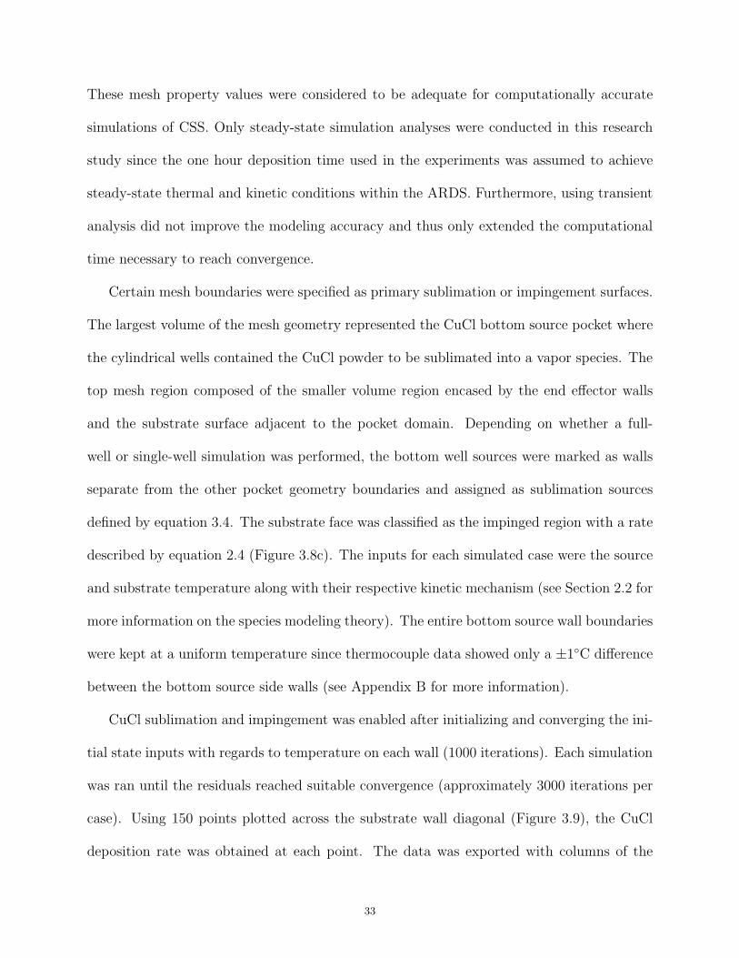
case). Using 150 points plotted across the substrate wall diagonal (Figure 3.9), the CuCl
deposition rate was obtained at each point. The data was exported with columns of the
33
Substrate
CuCl
Source
Pocket
(a) (b)
(c)
Figure 3.8. CuCl (a) mesh model used during FLUENT simulation, and(b) contour example when kinetic rates were activated to determine the CuClmass fraction throughout the pocket. This example was performed at a sub-strate and source temperature of 180.6◦C and 210◦C, respectively. (c) Speci-fied kinetic rates R1 and R2 at the bottom well source and top substrate wallboundaries, respectively.
deposition rate [nm/s] and location along the substrate diagonal [mm]. All deposition rates
were multiplied by t = 3600 s to determine what the predicted thickness would be after
one hour deposition and were compared to experimental results according to substrate and
source temperature parameters.
34
Figure 3.9. Examples of full well and single well simulation deposition rates.Along the black dotted line are where 150 points were mapped across the sub-strate diagonal to measure the deposition rate profile from position 3 to 7(referenced by Figure 3.5a) on the substrate for comparison to experimentalresults. These two examples were modeled at a substrate and source temper-ature of 191.7◦C and 210◦C, respectively.
35
CHAPTER 4
RESULTS/DISCUSSION
CuCl thicknesses were obtained for full-well CSS depositions as a function of substrate
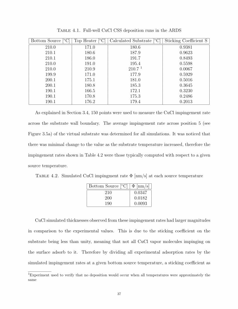
and source temperatures. Sticking coefficient values were calculated and plotted to develop
curve fitting parameters that would improve the initial accuracy of the full-well simulation
models. The converged model along with sticking coefficient curves for a given source tem-
perature was later applied to single-well depositions to verify its computational accuracy at
such a vastly different process condition. In order to gain a further understanding of the
inherent growth mechanisms exhibited by CuCl during CSS process conditions, characteriza-
tion via Scanning Electron Microscopy (SEM) and Electron Dispersion Spectroscopy (EDS)
were performed on the full-well experiments. This chapter aims to provide the aforemen-
tioned results while elaborating on their significance to CuCl thin-film deposition and growth
analysis. A discussion on the various implications within the data will be made, which will
be used to draw conclusions on the proposed CuCl growth mode as well as current modeling
accuracy in representing the CuCl vaporization process and the resulting thin-film uniformity
during CSS.
4.1. FULL-WELL DEPOSITION
As mentioned in Section 3.1, TEC-12D substrates initially entered the ARDS chamber
without prior heating, during which CuCl was deposited for one hour. Substrates with a
lower surface temperature during CSS deposition were visibly covered with a white-colored
film on the TCO layer, which became more transparent as the temperature increased. All
full-well depositions along with their average top heater, bottom source, and calculated
substrate temperatures are listed in Table 4.1.
36
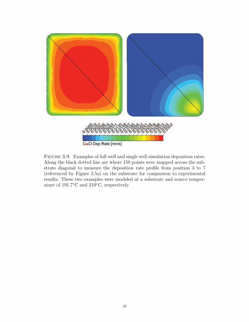
Table 4.1. Full-well CuCl CSS deposition runs in the ARDS
Bottom Source [◦C] Top Heater [◦C] Calculated Substrate [◦C] Sticking Coefficient S
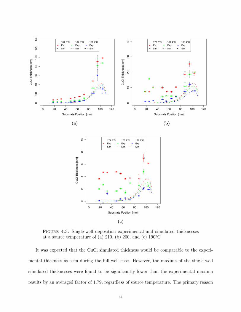
Figure 4.3. Single-well deposition experimental and simulated thicknessesat a source temperature of (a) 210, (b) 200, and (c) 190◦C
It was expected that the CuCl simulated thickness would be comparable to the experi-
mental thickness as seen during the full-well case. However, the maxima of the single-well
simulated thicknesses were found to be significantly lower than the experimental maxima
results by an averaged factor of 1.79, regardless of source temperature. The primary reason
44
that may explain such a discrepancy is related to a vapor pressure effect in the pocket. Since
the CuCl partial pressure is restricted to the volume of the pocket, no further sublimation
could take place without some type of deposition occurring on the CuCl domain walls or
until the substrate entered the domain. The greater number of sublimating wells in the
full-well case would be closer to the partial pressure saturation point, which would limit
the amount of sublimation. In contrast, the single-well sublimation case may not reach a
saturated pressure because the deposition rate on the substrate surface after entering the
domain is greater than the sublimation rate required to achieve an equilibrium vapor pres-
sure. In turn, this would cause most of what sublimates from the single well to adsorb to
the substrate and give a thickness near the full-well case. Considering these effects, the cur-
rent simulation model does not accommodate this limitation since it only uses the empirical
sublimation rate determined from the mass-loss experiment in Section 3.2. The B1 and C1
terms in equation 2.14 do not incorporate the changes in vapor pressure as expected. Thus
an equation that includes a pressure-dependent term is necessary to describe the changes to
sublimation due to CuCl vapor pressure4.
The second reason relates back to the growth mode of CuCl on the TCO layer. If the
CuCl overlayer preferentially forms islands, this would lead to a higher sticking probability
in isolated regions on the substrate and would dictate grain growth even if a uniform vapor
pressure was achieved in the pocket. This can be seen by looking at how CuCl growth
seems to occur in areas not directly in the line of sight of the filled CuCl single-well source.
In contingence with this result, all experiments had substantially thick, non-uniform films
in positions 3 and 5 of the substrate diagonal, especially for experiments in Figures 4.3b
and 4.3c. Once again, the Volmer-Weber growth mechanism is the most plausible explanation
4See Appendix C for more details
45
for this island growth of CuCl. Another explanation for this phenomenon is related to
secondary diffusion of the CuCl molecule that has not stuck to the surface. It is possible
that any of the impinging molecules that either desorb or reflect from the substrate may
enter the vapor species and diffuse further across the substrate and adsorb at a later time.
A more in-depth study on this effect needs to be done though to see how much it contributes
to island formation.
The aforementioned reasons explain why the simulated thicknesses are much smaller than
the experimental values in all single-well cases. The model did not predict any of the islands
forming on the surface nor did it accurately represent the vapor pressure effects that caused
the actual thicknesses to be similar to the full-well case despite less wells being filled. It is
obvious that there are major complexities that are unaccounted for in the current model of
CuCl thin-film growth and thus further refinement must be done to the simulation model.
It is necessary to implement both the CuCl growth mechanism and a vapor pressure term
to improve modeling accuracy of CuCl thin-film deposition.
4.3. SEM/EDS ANALYSIS
Despite other research studies evaluating the thin-film growth mode of CuCl deposited
on various substrate materials [19, 20, 40, 41], it was not known if similar behavior during
CSS would be prevalent for CuCl on the FTO layer. To assess the growth characteristics
of CuCl, SEM and EDS were performed on the full-well experiments in order to visually
analyze the effects of modulating the thermal conditions at both the substrate and source.
The following subsections will elaborate on the perceived trends that distinguish the CuCl
thin-film deposition and main growth mode responsible during CSS.
46
4.3.1. SEM ANALYSIS. The growth mechanism of CuCl during the substrate tem-
perature sweep was investigated using Scanning Electron Microscopy on position 8 of each
substrate sample (please refer to Figure 3.5). SEM was operated at 15 kV accelerating
voltage at 30,000⇥ magnification for all samples to keep consistency in visual comparison.
Figures 4.4a reveal the CuCl grains imaged when the substrate temperature was increased
from 180◦C to 210◦C while maintaining a source temperature of 210◦C. Grains in Figure 4.4a
are fully coalesced with few gaps between each large grain network. As the substrate tem-
perature increases (Figures 4.4b - 4.4d), the grain networks shrink toward the centers of each
grain and separate into regions of CuCl islands. As the substrate temperature approaches
the source temperature, CuCl vapor molecules no longer adsorb to the surface and as a
result leave a barren TCO layer (Figure 4.4e). To verify that Figure 4.4e is in fact the TCO
layer, a blank TEC-12D substrate was imaged as a means of validation (Figure 4.4f). As
expected, the TCO layers match from a visual perspective and are vastly different from the
CuCl grains seen in previous images.
Figures 4.5a - 4.5c depict the CuCl thin-film growth at a source temperature of 200◦C and
an increasing substrate temperature from 175 to 185◦C. Since the substrate temperatures
are closer to each other for this data set compared to the previously mentioned substrates at
a 210◦C source temperature, there are not striking differences between grain size. However,
in comparison to Figures 4.4a - 4.4e the grains have become smaller and appear to have nu-
cleation regions scattered between islands. Furthermore, as substrate temperature increases
there are slightly less CuCl grains across the imaged region.
The last full-well deposition runs were performed at a source temperature of 190◦C with
a varied substrate temperature from 170 to 180◦C (Figures 4.6a - 4.6c). The CuCl grains
are much smaller than the higher source temperature depositions, showing the influence of
47
the CuCl vapor species concentration on the overall thin-film growth. It is evident that the
onset of CuCl nucleation is occurring since the CuCl islands have greatly diminished and
the TCO layer below is visible throughout the imaged region.
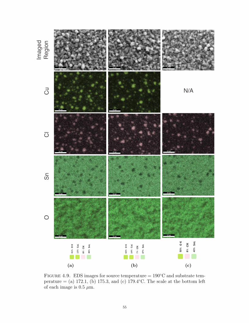
4.3.2. EDS ANALYSIS. EDS was performed in conjunction with the SEM images to
help support the claim that CuCl preferentially grows as island formations across the TCO
layer. This characterization technique was necessary in differentiating between CuCl islands
and the SnO layer beneath them by assessing the elemental composition of the imaged region.
All EDS results were performed at 7.5 kV accelerating voltage with a 20,000⇥ magnification
and drift correction enabled. Figures 4.7a - 4.7e display the mapping analysis of Cu, Cl, Sn,
and O normal to surface with respect to substrate temperature. The general trend shows the
CuCl grains shrinking and SnO signals expanding between islands as the surface temperature
increases toward the source temperature, whereupon in the final stage Cu and Cl signals are
undetectable. Again, coalescence is prevalent as lower temperatures while individual CuCl
islands exist at higher temperatures.
Overall the Cu and Cl signals in Figures 4.8a - 4.8c correlate with each other in their
mapped locations, indicating that the molecule is most likely non-dissociative during adsorp-
tion as assumed. This set of deposition runs had much smaller islands than previous EDS
images, which is in agreement with the expected trend of thinner CuCl films with decreasing
source temperature. The grains also become fewer with increasing substrate temperature.
As the source temperature decreases to 190◦C (Figures 4.9a - 4.9c), the Cu and Cl signals
disappear until there is minimal Cu on the surface with only Cl leftover on the Sn and O
rich areas. Such tiny grains are indicative of the onset of nucleation prior to island-by-island
formation as seen in previous results, which again leads back to the conclusion that the
Volmer-Weber growth mode is responsible for such growth.
48
4.3.3. SUMMARY. Evaluating all of the SEM/EDS images for full-well depositions
elucidates a number of CuCl growth characteristics. It is obvious that as the substrate
temperature increases, the CuCl grain size decreases with islands becoming more prominent
versus layer-by-layer films seen in Stranski-Krastanov growth [42]. This phenomenon is in
contrast to that observed during the studies on CuCl/MgO interfaces [19, 20], and thus
the results in this research suggest that the Volmer-Weber growth mode seen in the SEM
and EDS images is the dominant interaction mode between CuCl adsorbed molecules on
a Fluorine-doped Tin Oxide layer. Such a growth mode is not favored in other thin-film
semiconductor materials used in the ARDS such as CdS, which typically exhibits an S-K
growth mode [43]. Therefore it becomes increasingly important to control how much Cu is
used to dope the CdTe absorber layer. Despite this being a 2nd or 3rd order contributor
to the Cu doping issue, too much CuCl impinging on the CdTe surface may lead to Cu
island non-uniformities at the exposed CdTe interface. It is possible that the Cu would
diffuse into CdTe at higher concentrations where island formation is prominent, resulting in
non-uniform carrier transfer regions that may decrease solar cell efficiencies. However, this is
merely speculation based off of the current findings and requires much deeper characterization
analysis to understand in detail. Furthermore, this research study only focused on the
CuCl/TCO interface rather than extending it to CuCl/CdTe, which is the primary deposition
sequence in the ARDS. The reason for studying the former in detail was to gain a general
understanding of CuCl thin-film growth without the added complexity of species diffusion
or migration that exists in the latter case. Nonetheless, the CuCl thin-film growth results
for SEM/EDS reveal that Volmer-Weber growth is the mode responsible in CuCl thin-film
deposition within the CSS process.
49
(a) (b)
(c) (d)
(e) (f)
Figure 4.4. SEM images for source temperature = 210◦C and substrate tem-perature = (a) 180.6, (b) 187.9, (c) 191.7, (d) 195.4, and (e) 210.7◦C. (f) SEMimage of TCO layer only on TEC-12D substrate (no deposition) as a visualcomparison with (e). The scale on the bottom right of each image is 100 nm.
50
(a)
(b)
(c)
Figure 4.5. SEM images for source temperature = 200◦C and substrate tem-perature = (a) 177.9, (b) 181.0, and (c) 185.3◦C. The scale on the bottom rightof each image is 100 nm.
51
(a)
(b)
(c)
Figure 4.6. SEM images for source temperature = 200◦C and substrate tem-perature = (a) 177.9, (b) 181.0, and (c) 185.3◦C. The scale on the bottom rightof each image is 100 nm.
52
(a) (b) (c) (d) (e)
Figure 4.7. EDS images for source temperature = 210◦C and substrate tem-perature = (a) 180.6, (b) 187.9, (c) 191.7, (d) 195.4, and (e) 210.7◦C. The scaleat the bottom left of each image is 0.5 µm.
53
(a) (b) (c)
Figure 4.8. EDS images for source temperature = 200◦C and substrate tem-perature = (a) 177.9, (b) 181.0, and (c) 185.3◦C. The scale at the bottom leftof each image is 0.5 µm.
54
(a) (b) (c)
Figure 4.9. EDS images for source temperature = 190◦C and substrate tem-perature = (a) 172.1, (b) 175.3, and (c) 179.4◦C. The scale at the bottom leftof each image is 0.5 µm.
55
CHAPTER 5
CONCLUSION/FUTURE WORK
5.1. CONCLUSION
CuCl thin-film growth was explored while varying CSS thermal parameter conditions.
By gaining insight on how CuCl deposits on the substrate, a general assessment could be de-
veloped as to what heating temperatures within the CuCl domain will give the most uniform
deposition across the entire substrate. The uniformity of Cu doping in the CdTe absorber
layer has been a challenging issue within thin-film solar cell fabrication. The ultimate goal
for this study was to devise a means of predicting the CuCl uniformity within the ARDS
that would lead to an overall understanding of the CuCl vaporization process. The compu-
tationally accurate model would then be used to determine a CSS operation range capable
of achieving an optimal solution for Cu doping in the CdTe absorber layer.
Results on the CuCl mass-loss experiment point out the necessity of obtaining an Ar-
rhenius expression for the CuCl sublimation rate at a higher pressure regime than most
literature [7, 27–29]. Such a study was crucial in providing an accurate kinetic vapor rate in
CSS modeling because of its direct contribution to the impingement rate as shown in equa-
tion 2.4. With such data, a more representative species concentration was seen within the
CuCl pocket that proportionally changed the deposition rate on the substrate mesh bound-
ary. Furthermore, the derived Arrhenius expression was used for several source temperature
values so that a wide range of simulations could be completed with minimal inputs by the
program user. In spite of the CuCl mass-loss data found for the full-well case, applying
the same Arrhenius expression to the single-well modeling case and comparing to the ex-
perimental results demonstrated a significantly less sublimation rate than the latter. It was
56
speculated that the single-well experiment did not completely reach an equilibrium vapor
pressure in the pocket since the already low CuCl gas concentration was rapidly deposited
on the substrate. This would consequentially drive the single well source to further subli-
mation to compensate for the lack of a saturated pressure condition. Such circumstances
would explain why more sublimation would occur and thus give a higher CuCl thickness
measurement than the model originally proposed. The single-well modeling results prove
that the CuCl model in an extreme deposition case was not quantitatively accurate and thus
requires more development to become a high-fidelity computational simulation.
The full-well simulations and experiments were used to determine an S curve fit for each
particular source temperature. All sticking coefficients for a given substrate temperature
were found using equation 2.5 with the experimental adsorption rate and calculated im-
pingement rate as inputs. Equation 4.1 was then fitted to the sticking coefficient values at
various substrate and source temperatures and applied to each full-well simulation model for
further computational accuracy. The model was able to converge to the average CuCl thick-
ness experimental results but could not accurately represent the thickness non-uniformities
present in all experiments. This is due to the simplistic modeling conditions at the substrate
wall, which lack a growth mode algorithm that enables dynamic interaction between the gas
and site species on its boundary (i.e. nucleation, islanding, percolation, and coalescence). A
number of CuCl depositions were relatively thicker on position 3 of the substrates and may
indicate that some type of gradient exists in the pocket. However it is not exactly known
whether a substrate temperature or species concentration gradient is responsible for the is-
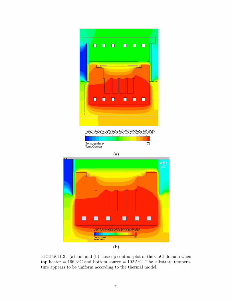
sue. The thermal modeling conducted on the CuCl domain in the ARDS seems to refute
the possibility of a thermal gradient across the substrate or the CuCl bottom source. If the
thermal modeling results are valid, then the only sound explanation would be some type of
57
small gap between the substrate and end effector that is causing CuCl vapor to deposit more
readily on one side of the substrate.
An in-depth observation of the SEM/EDS results showed that in general the CuCl grains
diminish in size and number at higher substrate temperatures. SEM revealed such a pattern
when the coalescence of large CuCl grain networks eventually separated into smaller islands
with increasing substrate temperatures. EDS mapping further validated this phenomenon
by showing the Cu and Cl island signals decreasing with Sn and O counts increasing between
island regions. Eventually the Sn and O signals dominated the entire mapped region as the
substrate temperature reached the source temperature. Across lower source temperature
mappings, the grains were significantly smaller than the largest source temperature data
and consistently depicted nucleation islands as oppose to uniform CuCl layers. In summary,
CuCl thin-films grown on FTO-coated substrates exhibit the Volmer-Weber growth mode by
first forming islands and then coalescing to develop large grain networks across the exposed
surface.
Following the full-well CSS experiments, single-well deposition runs were performed to
check the fidelity of the simulation model in an extreme process condition. It was concluded
that the model did qualitatively predict the hill-top shape of single-well CuCl thin-film
growth but did not effectively represent the varying surface topologies displayed in most
single-well CuCl experiments. The current simulation model can at the very least provide
an accurate computation of the CuCl sublimation process that predicts the average CuCl
thickness based on the CSS thermal conditions. This demonstrates that the CFD-based
CuCl thin-film growth simulation during CSS is moving in the right direction and can be
improved for more complex kinetic phenomena or applied to various domain geometries.
58
5.2. FUTURE WORK
There are many opportunities to enhance the current simulation model. The discrepan-
cies between the predicted thickness and the experimental results is mainly due to the lack
of particle surface interactions that occur on a nanoscale. By assuming that the site species
remained constant throughout deposition, no method was assigned that accommodated for
the roughness across the substrate after CuCl adsorption. In turn, the steady-state solution
for the deposition rate remained ideally uniform since there were no influences from adjacent
mesh layers over time. One way to integrate a physical change to the wall surface over time
would be to create a time-dependent dynamic mesh surface accompanied by a user-defined
function that models the growth mode at a given interface. Surface energies at each node
of the substrate wall and dimensional cell parameters such as tilt angle and face size would
be collected and processed with respect to time. CuCl thin-film topologies could then be
manipulated on the substrate mesh body, acting in essence as a pseudo-transient surface that
changes in response to the fluctuation of CuCl site species at each time step. Such a model
would act in place of a molecular dynamics simulation of deposition rate while retaining its
continuum-based species algorithms.
Experiments with CuCl deposition to a CdTe layer would be another major next step in
this work. CdTe is significantly thicker and rougher than CuCl at only 110 s deposition on the
substrate, so it would be necessary to obtain a thin-layered CdTe (⇡ 100 nm) with properties
comparable to its thicker predecessor. A thin CdTe layer would also make it possible to use
the current Argon Ion Beam Sputtering method to measure the crater depths with SWLI.
If there is any concern for HCl etching at the bottom CdTe layer, a less aggressive solution
such as methanol or IPA could be used in place for removing the CuCl overlayer. After
refinement and execution of the previously mentioned simulation improvement, a new mesh
59
layer interface such as CdTe could be created on the pre-existing TCO mesh to check how
the deposition rate changes. Since Cu diffusion and migration would be of interest, inclusion
of Te site species that interact with Cu and sink regions that effectively remove the CuCl
concentration near the CdTe boundary would be required for accurate diffusion analysis. A
FLUENT simulation of the CuCl/CdTe interface would offer the most useful knowledge to
the growth rates in this region and how they affect Cu diffusion into CdTe.
Analysis of CuCl thin-film deposition and growth at various process conditions with
a computational model demonstrates the versatility of using simulation alongside theory
and experimentation in the research process. With the current understanding of thin-film
deposition by CSS, it is now possible to extend the modeling structure applied in this research
study to other materials or thin-film deposition techniques besides Close-Space Sublimation.
It is thus apparent that simulation can play an influential role in thin-film manufacturing
processes and open up other avenues of exploration for thin-film deposition and growth.
60
BIBLIOGRAPHY
[1] F. Breitenecker and I. Troch, “Simulation Software - Development and Trends,” in
Control Systems, Robotics, and Automation (H. Unbehauen, ed.), vol. IV, EOLSS, 2009.
[2] J. D. Anderson Jr., Computational Fluid Dynamics. 3rd ed., 2009.
[3] G. E. Moore, “Cramming More Components into Integrated Circuits,” in Proceedings
of the IEEE, vol. 86, pp. 82–85, January 1998.
[4] F. Hosseinpour and H. Hajihosseini, “Importance of Simulation in Manufacturing,”
International Journal of Social, Behavioral, Educational, Economic, Business and In-
dustrial Engineering, vol. 3, pp. 229–232, 2009.
[5] D. A. Bodner and L. F. McGinnis, “A Structured Approach to Simulation Modeling
of Manufacturing Systems,” in Industrial Engineering Research Conference, (Georgia
Institute of Technology, Atlanta, GA), 2002.
[6] D. R. Hemenway, “Computational Modeling of Cadmium Sulfide Deposition in the
CdS/CdTe Solar Cell Manufacturing Process,” Master’s thesis, Colorado State Univer-
sity, Fort Collins, CO, 2013.
[7] D. F. Brestovanksy et al., “Analysis of the rate of vaporization of CuCl for solar cell
fabrication,” Journal of Vacuum Science & Technology A, vol. 1, pp. 28–33, 1983.
[8] M. Burgelman and A. de Vos, “Evaporation of CuCl and CuCl2 for the fabrication of
Cu2S/CdS thin film solar cells,” Thin Solid Films, vol. 102, pp. 367–374, 1983.
[9] T. S. Te Velde, “The production of the Cadmium Sulphie-Copper Sulphide Solar Cell
by means of a Solid-state Reaction,” Energy Conversion, vol. 15, pp. 111–115, 1975.
[10] B. E. McCandless and J. R. Sites, “Cadmium Telluride Solar Cells,” in Handbook of
Photovoltaic Science and Engineering (A. Luque and S. Hegedus, eds.), John Wiley &
Sons, Ltd, 2003.
61
[11] D. E. Swanson et al., “Single vacuum chamber with multiple close space sublimation
sources to fabricate CdTe solar cells,” Journal of Vacuum Science & Technology A,
vol. 34, pp. 021202–1–021202–6, 2016.
[12] V. V. Plotnikov, X. Liu, and A. D. Compaan, “Studies of Cu location near the back
contact of CdS/CdTe solar cells,” in Photovoltaic Specialist Conference (PVSC), 2008
IEEE 33rd, (University of Toledo, Toledo, OH), 2008.
[13] C. S. Ferekides et al., “An effective method of Cu incorporation in CdTe solar cells for
improved stability,” Thin Solid Films, pp. 5833–5836, 2007.
[14] F. Bechstedt, Principles of Surface Physics. Springer-Verlag Berlin Heidelberg, 2003.
[15] A. Grob, Theoretical Surface Science. Springer-Verlag Berlin Heidelberg, 2nd ed., 2009.
[16] J. L. Cruz-Campa and D. Zubia, “CdTe thin film growth model under CSS conditions,”
Solar Energy Materials & Solar Cells, vol. 93, pp. 15–18, 2009.
[17] S. Miyamoto, “A Theory of the Rate of Sublimation,” Bulletin of the Chemical Society
of Japan, pp. 794–797, 1933.
[18] M. Ohring, Materials Science of Thin Films. 2nd ed., 2001.
[19] A. Yanase and Y. Segawa, “Two different in-plane orientations in the growths of cuprous
halides on MgO(001),” Surface Science, vol. 329, pp. 219–226, 1995.
[20] A. Yanase and Y. Segawa, “Stranski-Krastanov growth of CuCl on MgO(001),” Surface
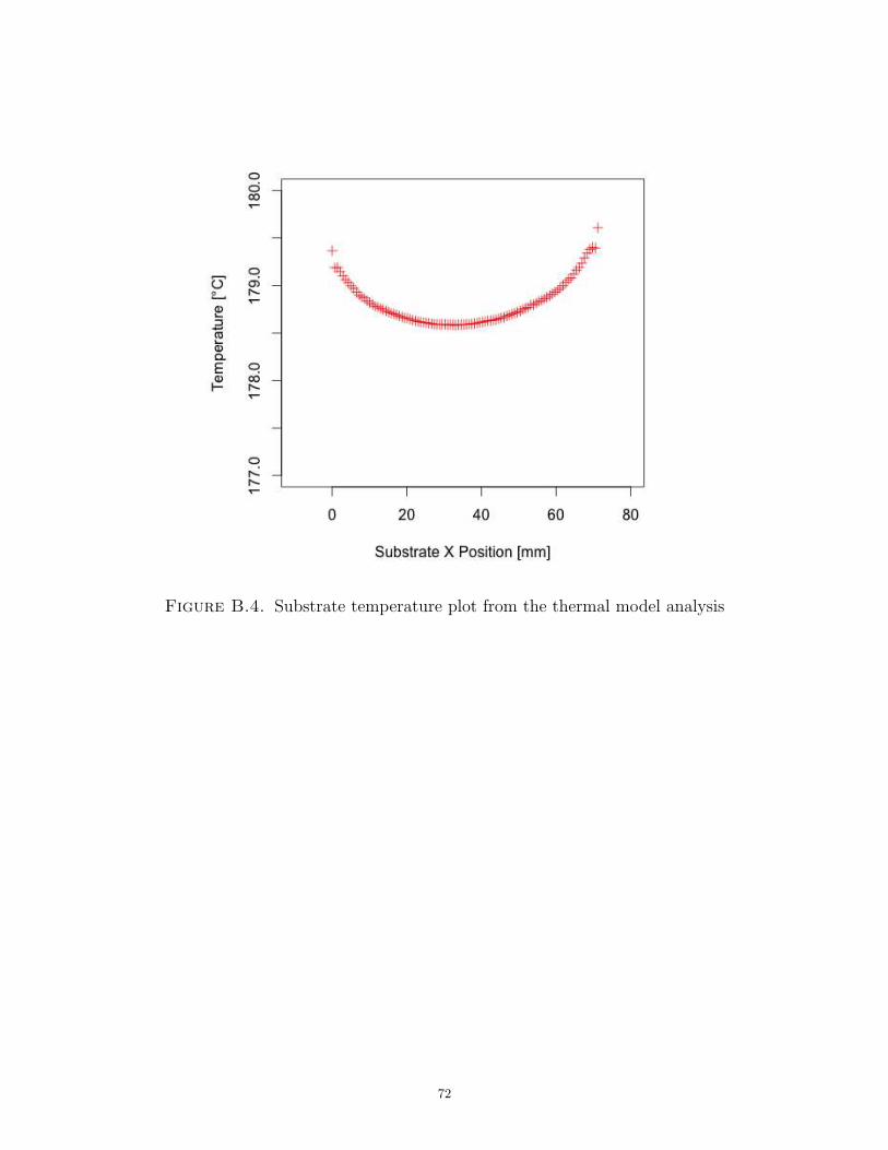
Measurements were taken 6 times at 2 minute intervals for statistical validation. The results
at each source temperature are presented in Figures B.2a - B.2f. The overall trend of the
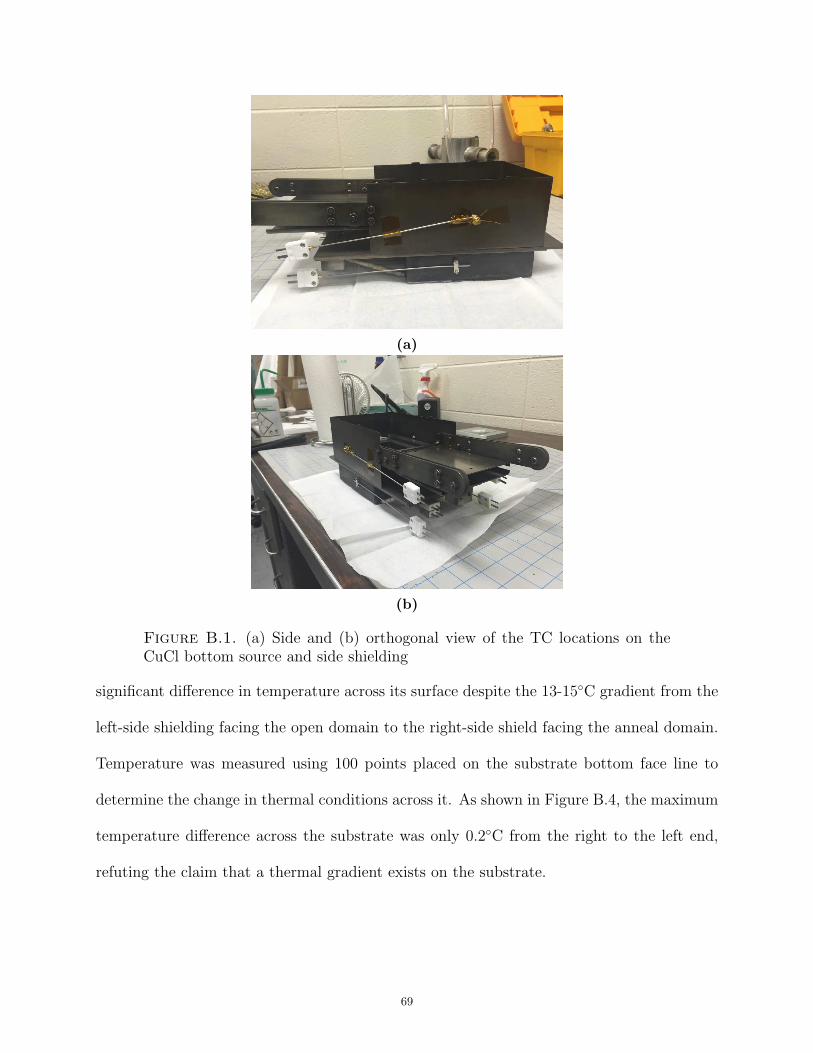
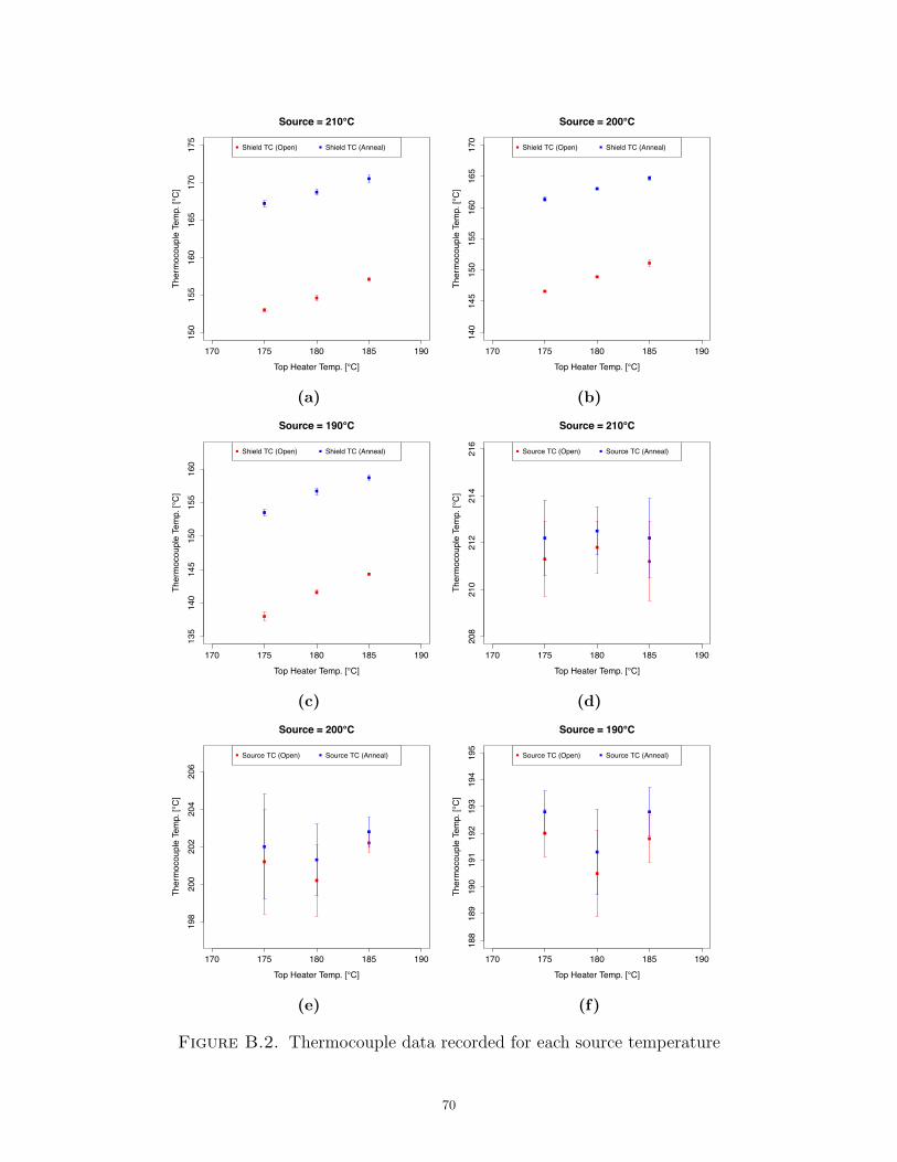
data is that the side shielding had a 13-15◦C change due to the open and anneal domains
adjacent to the CuCl domain, as well as the 1◦C difference for the CuCl bottom source walls.
The large error bars on the bottom source TCs were due to the PID modulation and provide
no other useful information.
A thermal model of the CuCl domain was created to calculate the temperature through-
out the CuCl chamber region. Figures B.3a and B.3b provide a contour plot of the thermal
modeling results when the TC data was obtained at bottom source and top heater tempera-
tures of 192.5◦C and 166.3◦C, respectively. The plots show that the substrate does not see a
68
(a)
(b)
Figure B.1. (a) Side and (b) orthogonal view of the TC locations on theCuCl bottom source and side shielding
significant difference in temperature across its surface despite the 13-15◦C gradient from the
left-side shielding facing the open domain to the right-side shield facing the anneal domain.
Temperature was measured using 100 points placed on the substrate bottom face line to
determine the change in thermal conditions across it. As shown in Figure B.4, the maximum
temperature difference across the substrate was only 0.2◦C from the right to the left end,
refuting the claim that a thermal gradient exists on the substrate.
69
170 175 180 185 190
15
01
55
16
01
65
17
01
75
Source = 210°C
Top Heater Temp. [°C]
Th
erm
oco
up
le T
em
p.
[°C
]
Shield TC (Open) Shield TC (Anneal)
(a)
170 175 180 185 190
14
01
45
15
01
55
16
01
65
17
0
Source = 200°C
Top Heater Temp. [°C]
Th
erm
oco
up
le T
em
p.
[°C
]
Shield TC (Open) Shield TC (Anneal)
(b)
170 175 180 185 190
13
51
40
14
51
50
15
51
60
Source = 190°C
Top Heater Temp. [°C]
Th
erm
oco
up
le T
em
p.
[°C
]
Shield TC (Open) Shield TC (Anneal)
(c)
170 175 180 185 190
20
82
10
21
22
14
21
6
Source = 210°C
Top Heater Temp. [°C]
Th
erm
oco
up
le T
em
p.
[°C
]Source TC (Open) Source TC (Anneal)
(d)
170 175 180 185 190
19
82
00
20
22
04
20
6
Source = 200°C
Top Heater Temp. [°C]
Th
erm
oco
up
le T
em
p.
[°C
]
Source TC (Open) Source TC (Anneal)
(e)
170 175 180 185 190
18
81
89
19
01
91
19
21
93
19
41
95
Source = 190°C
Top Heater Temp. [°C]
Th
erm
oco
up
le T
em
p.
[°C
]
Source TC (Open) Source TC (Anneal)
(f)
Figure B.2. Thermocouple data recorded for each source temperature
70
(a)
(b)
Figure B.3. (a) Full and (b) close-up contour plot of the CuCl domain whentop heater = 166.3◦C and bottom source = 192.5◦C. The substrate tempera-ture appears to be uniform according to the thermal model.
71
Figure B.4. Substrate temperature plot from the thermal model analysis
72
APPENDIX C
SUBLIMATION RATE PRESSURE DEPENDENCE
The theory of the sublimation rate [17] is fully expressed as follows:
(C.1)dm
dt= A·
pT · e(
−λRT ) − S · P
r
M
2⇡RT
where A is the pre-exponential factor, T is temperature of the gas, λ is the activation
energy of evaporation, S is the sticking coefficient, P is the partial pressure of the gas, M is
the molar mass of the gas, and R is the gas constant. It should be apparent from this equation
that sublimation depends on both the rate of evaporation and the rate of condensation at
the solid-gas interface. When the entire pocket containing the gas achieves an equilibrium
vapor pressure condition, the sublimation rate is impeded (dmdt
= 0) and thus the expression
becomes:
(C.2) A·pT · e(
−λRT ) = S · P1
r
M
2⇡RT
where P1 is the vapor pressure of the gas. Therefore the sublimation rate can be redefined
in terms of both temperature and partial pressure of the gas:
(C.3)dm
dt= S
r
M
2⇡RT(P1 − P )
The sublimation rate used in this particular study for CuCl was represented as an Arrhe-
nius rate expression (equation 2.2) that did not include the vapor pressure term P in order to
study only the thermal aspects associated with sublimation and thin-film deposition. How-
ever, it was seen later in the research process that one of the main reasons the computational
73
model was not as accurate for the single-well case was to due to not accommodating the va-
por pressure effects in the CuCl pocket domain. That is why a vapor pressure-dependent
equation similar to equation C.3 needs to be somehow derived within the experimental subli-
mation rate data described in Section 3.2. Furthermore, such an equation needs to be applied
to the simulation for improved accuracy in predicting the CuCl thin-film non-uniformities
present across the substrate. This may require more sublimation experiments, in particular
the single-well case instead of another full-well case, to see the differences in sublimation rate
and how they relate to vapor pressure. This generalized expression would be an immediate