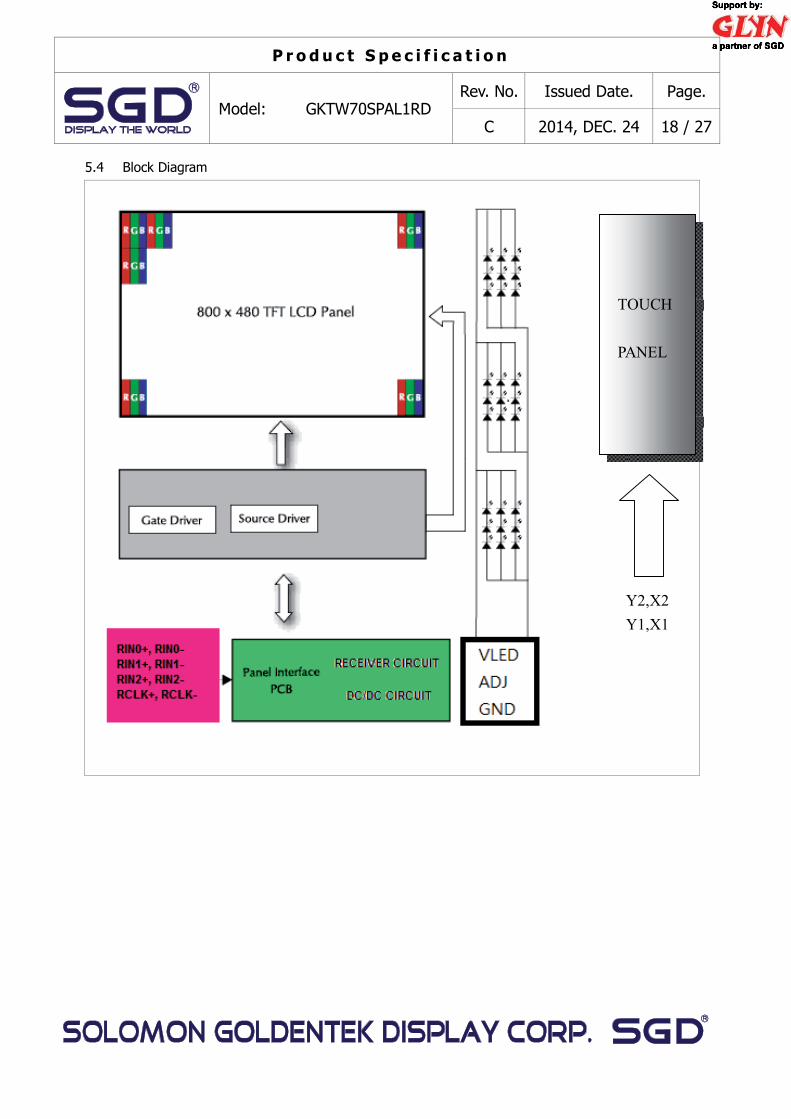
GKTW70SPAL1RD is a transmissive type color active matrix TFT (Thin Film Transistor) liquid crystal display (LCD) that uses amorphous silicon TFT as a switching device. This model is composed of a TFT-LCD module, a receiver circuit, touch Panel and a back-light unit. Graphics and texts can be displayed on a WVGA 800 (W) x 3 x 480 (H) dots (16:9 aspect ratio) with 262,144 colors by supplying 18 bits data signal (6bits/each color). The following table described the features of GKTW70SPAL1RD. 1.1 Features
- Transmissive and back-light with 27 LEDs are available. - TN (Twisted Nematic) mode. - LVDS Receiver 18 bit Interface. - Back-light Dimming control - 4-wire Touch Panel
1.2 LCD Module
Item Specification Unit
Screen Size 7.0 inches Diagonal
Display Resolution 800 (H) x 480 (V) Pixel
Active Area 153.6 (H) x 86.64 (V) mm
Outline Dimension 165.00 (H) x 104.00 (V) x 6.5 (T) mm
Display Mode Normally white mode/ Transmissive --
Surface Treatment Anti-glare(AG),3H --
Pixel Arrangement R,G,B Vertical Stripe --
Pixel Size 192 x 180.5 um
Display Color 262k --
Viewing Direction 6 o’clock --
Input Interface LVDS Receiver 18 bit Interface --
2. Mechanical Information
Item Min. Typ. Max. Unit Note
Module Size
Horizontal (H) -- 165.00 -- mm
Vertical (V) -- 104.00 -- mm
Thickness (T) -- 6.5 -- mm (1)
Weight -- (165) -- g --
Note (1) Not Include Component. Refer to the Outline Dimension Drawing as attached.
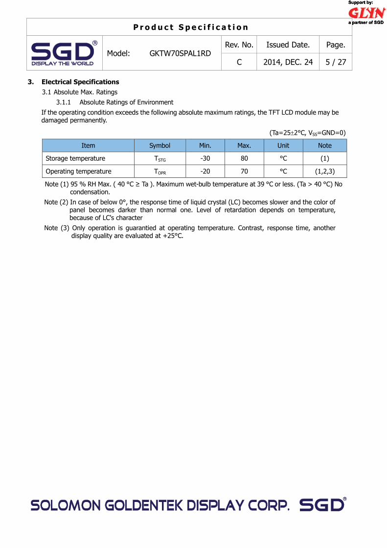
3.1.1 Absolute Ratings of Environment If the operating condition exceeds the following absolute maximum ratings, the TFT LCD module may be damaged permanently.
(Ta=25±2°C, VSS=GND=0)
Item Symbol Min. Max. Unit Note
Storage temperature TSTG -30 80 °C (1)
Operating temperature TOPR -20 70 °C (1,2,3)
Note (1) 95 % RH Max. ( 40 °C ≥ Ta ). Maximum wet-bulb temperature at 39 °C or less. (Ta > 40 °C) No condensation.
Note (2) In case of below 0°, the response time of liquid crystal (LC) becomes slower and the color of panel becomes darker than normal one. Level of retardation depends on temperature, because of LC's character
Note (3) Only operation is guarantied at operating temperature. Contrast, response time, another display quality are evaluated at +25°C.
P r o d u c t S p e c i f i c a t i o n
Model: GKTW70SPAL1RD Rev. No. Issued Date. Page.
C 2014, DEC. 24 6 / 27
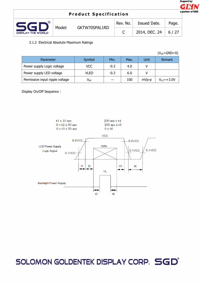
3.1.2 Electrical Absolute Maximum Ratings
(VSS=GND=0)
Parameter Symbol Min. Max. Unit Remark
Power supply Logic voltage VCC -0.3 4.0 V
Power supply LED voltage VLED -0.3 6.0 V
Permissive input ripple voltage VRF -- 100 mVp-p VCC=+3.0V
Display On/Off Sequence :
P r o d u c t S p e c i f i c a t i o n
Model: GKTW70SPAL1RD Rev. No. Issued Date. Page.
C 2014, DEC. 24 7 / 27
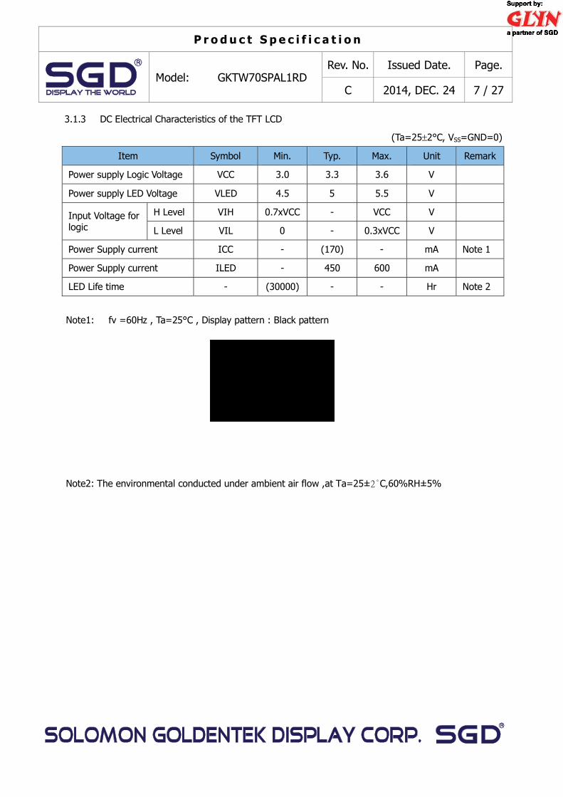
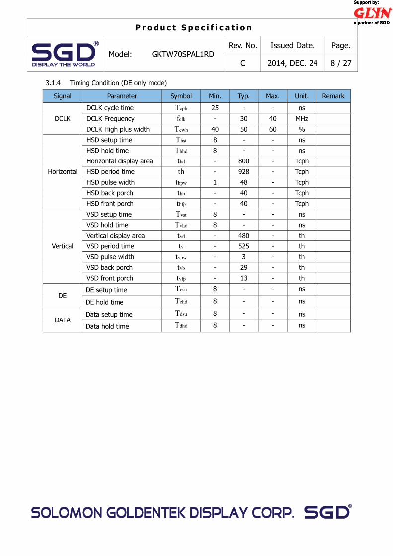
3.1.3 DC Electrical Characteristics of the TFT LCD
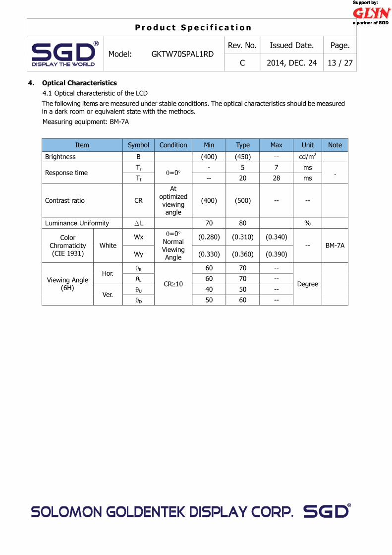
4. Optical Characteristics 4.1 Optical characteristic of the LCD The following items are measured under stable conditions. The optical characteristics should be measured in a dark room or equivalent state with the methods. Measuring equipment: BM-7A
Item Symbol Condition Min Type Max Unit Note
Brightness B (400) (450) -- cd/m2
Response timeTr
θ=0°- 5 7 ms
.Tf -- 20 28 ms
Contrast ratio CR
At optimized viewing angle
(400) (500) -- --
Luminance Uniformity L 70 80 %
Color Chromaticity (CIE 1931)
White Wx θ=0°
Normal Viewing Angle
(0.280) (0.310) (0.340) -- BM-7A
Wy (0.330) (0.360) (0.390)
Viewing Angle (6H)
Hor. θR
CR≥10
60 70 --
Degree θL 60 70 --
Ver. θU 40 50 --
θD 50 60 --
P r o d u c t S p e c i f i c a t i o n
Model: GKTW70SPAL1RD Rev. No. Issued Date. Page.
C 2014, DEC. 24 14 / 27
a. Test equipment setup
After stabilizing and leaving the panel alone shall be warmed up for the stable operation of LCM, the measurement should be executed. Measurement should be executed in a stable, windless, and dark room. Optical specifications are measured by Topcon BM-7A(fast) with a viewing angle of 2° at a distance of 50cm and normal direction.
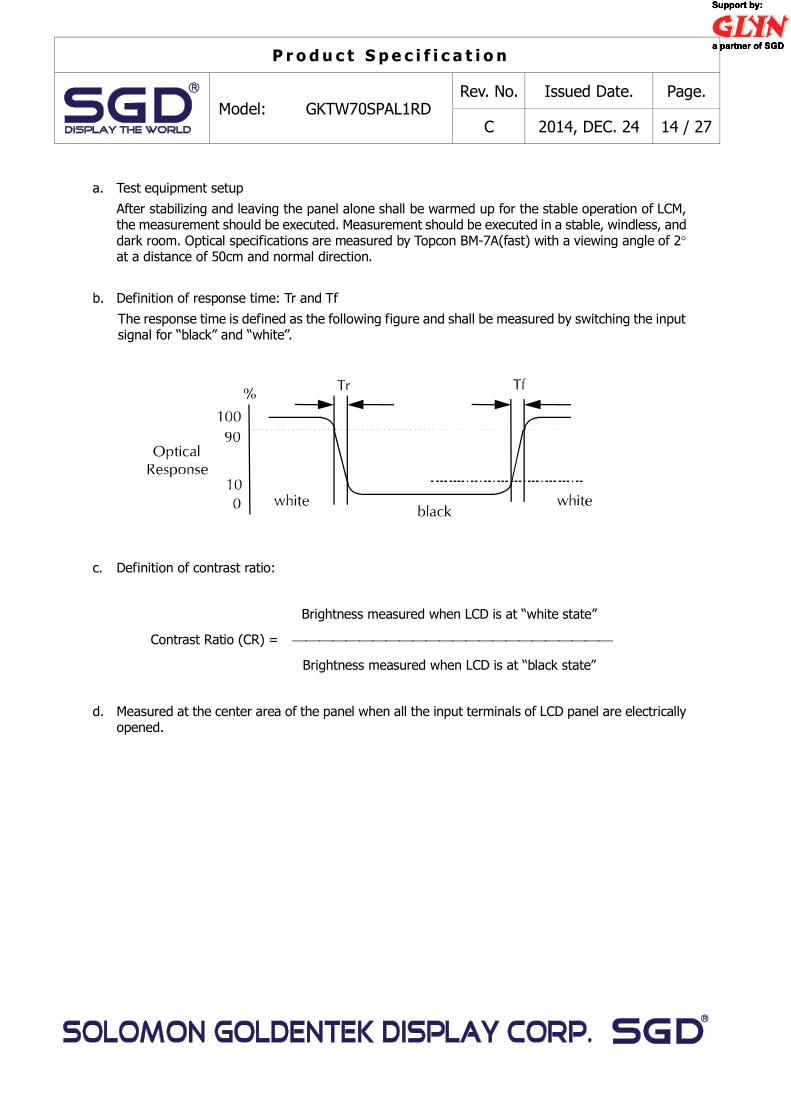
b. Definition of response time: Tr and Tf
The response time is defined as the following figure and shall be measured by switching the input signal for “black” and “white”.
c. Definition of contrast ratio:
Brightness measured when LCD is at “white state”
Contrast Ratio (CR) = ⎯⎯⎯⎯⎯⎯⎯⎯⎯⎯⎯⎯⎯⎯⎯⎯⎯⎯⎯⎯⎯⎯⎯⎯
Brightness measured when LCD is at “black state”
d. Measured at the center area of the panel when all the input terminals of LCD panel are electrically
opened.
P r o d u c t S p e c i f i c a t i o n
Model: GKTW70SPAL1RD Rev. No. Issued Date. Page.
C 2014, DEC. 24 15 / 27
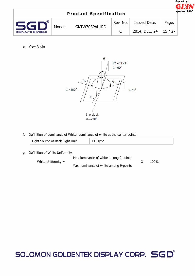
e. View Angle
f. Definition of Luminance of White: Luminance of white at the center points
Light Source of Back-Light Unit LED Type
g. Definition of White Uniformity
Min. luminance of white among 9-points White Uniformity = ⎯⎯⎯⎯⎯⎯⎯⎯⎯⎯⎯⎯⎯⎯⎯⎯⎯⎯⎯ X 100%
Max. luminance of white among 9-points
P r o d u c t S p e c i f i c a t i o n
Model: GKTW70SPAL1RD Rev. No. Issued Date. Page.
C 2014, DEC. 24 16 / 27
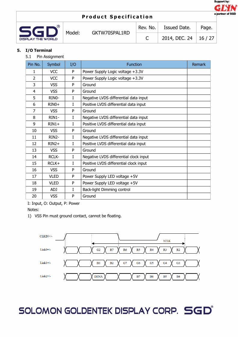
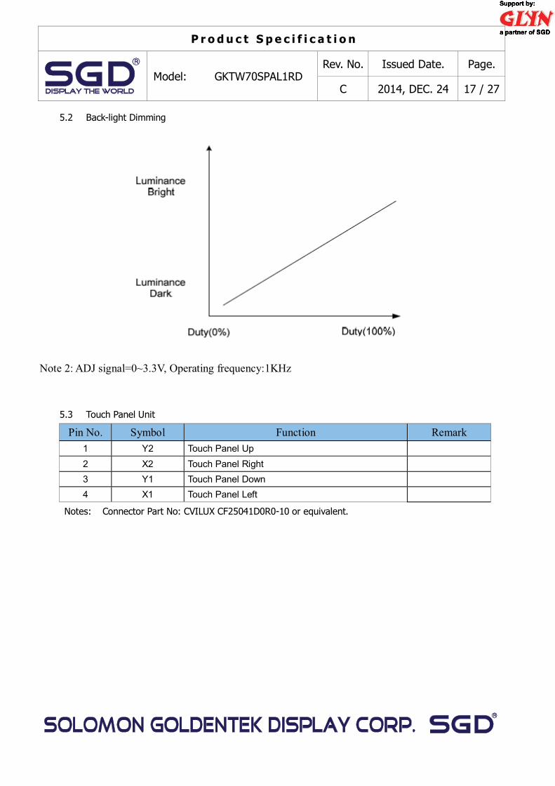
5. I/O Terminal 5.1 Pin Assignment
Pin No. Symbol I/O Function Remark
1 VCC P Power Supply Logic voltage +3.3V
2 VCC P Power Supply Logic voltage +3.3V
3 VSS P Ground
4 VSS P Ground
5 RIN0- I Negative LVDS differential data input
6 RIN0+ I Positive LVDS differential data input
7 VSS P Ground
8 RIN1- I Negative LVDS differential data input
9 RIN1+ I Positive LVDS differential data input
10 VSS P Ground
11 RIN2- I Negative LVDS differential data input
12 RIN2+ I Positive LVDS differential data input
13 VSS P Ground
14 RCLK- I Negative LVDS differential clock input
15 RCLK+ I Positive LVDS differential clock input
16 VSS P Ground
17 VLED P Power Supply LED voltage +5V
18 VLED P Power Supply LED voltage +5V
19 ADJ I Back-light Dimming control
20 VSS P Ground
I: Input, O: Output, P: PowerNotes: 1) VSS Pin must ground contact, cannot be floating.
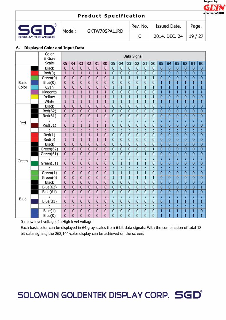
0 : Low level voltage, 1 :High level voltage Each basic color can be displayed in 64 gray scales from 6 bit data signals. With the combination of total 18 bit data signals, the 262,144-color display can be achieved on the screen.
Transparency - 78 - % Non-glare Caution (1) : Do not operate it with a thing except a polyacetal pen (tip R0.8mm or less) or a finger, especially those with hard or sharp tips such as a ball point pen or a mechanical pencil.
7.1.2 Mechanical & Reliability Characteristics
Item Min. Typ. Max. Unit Note
Activation force 60 80 100 g (1)
Hitting Durability 1,000,000 - - times (2)
Sliding Durability 100,000 times
Surface hardness 3 - - H JIS K5400
Note (1) Input : Finger or polyacetal pen 0.8R Note (2) Pit 1,000,000 times on the Film with a R8.0 (Hardness 60°) silicon rubber. - Force : Force : 200g - Frequency : 2 times/sec
P r o d u c t S p e c i f i c a t i o n
Model: GKTW70SPAL1RD Rev. No. Issued Date. Page.
C 2014, DEC. 24 21 / 27
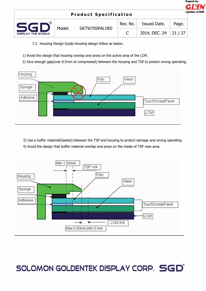
7.2 Housing Design Guide Housing design follow as below.
1) Avoid the design that housing overlap and press on the active area of the LCM.
2) Give enough gap(over 0.5mm at compressed) between the housing and TSP to protect wrong operating.
3) Use a buffer material(Gasket) between the TSP and housing to protect damage and wrong operating.
4) Avoid the design that buffer material overlap and press on the inside of TSP view area.
P r o d u c t S p e c i f i c a t i o n
Model: GKTW70SPAL1RD Rev. No. Issued Date. Page.
C 2014, DEC. 24 22 / 27
8. Reliability Condition No change on display and in operation under the following test condition. Condition: Unless otherwise specified, tests will be conducted under the following condition. Temperature: 20±5°C. Humidity: 65±5%RH. Tests will be not conducted under functioning state.
No. Parameter Condition Notes
1 High Temperature Operating 70°C±2°C, 240hrs (Operation state).
2 Low Temperature Operating -20°C±2°C, 240hrs (Operation state). 1
3 High Temperature Storage 80°C±2°C, 240hrs. 2
4 Low Temperature Storage -30°C±2°C, 240hrs. 1,2
5 High Temperature and High Humidity Operation Test
50°C±2°C, 90 , 240hrs. 1,2
6 Vibration Test
Total fixed amplitude: 1.5mm. Vibration Frequency: 10∼55Hz. One cycle 60 seconds to 3 direction of X, Y, Z each 15 minutes.
3
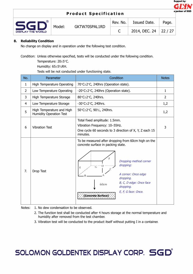
7. Drop Test
To be measured after dropping from 60cm high on the concrete surface in packing state.
Dropping method corner dropping: A corner: Once edge dropping. B, C, D edge: Once face dropping.
E, F, G face: Once.
Notes: 1. No dew condensation to be observed. 2. The function test shall be conducted after 4 hours storage at the normal temperature and
humidity after removed from the test chamber. 3. Vibration test will be conducted to the product itself without putting I in a container.
P r o d u c t S p e c i f i c a t i o n
Model: GKTW70SPAL1RD Rev. No. Issued Date. Page.
C 2014, DEC. 24 23 / 27
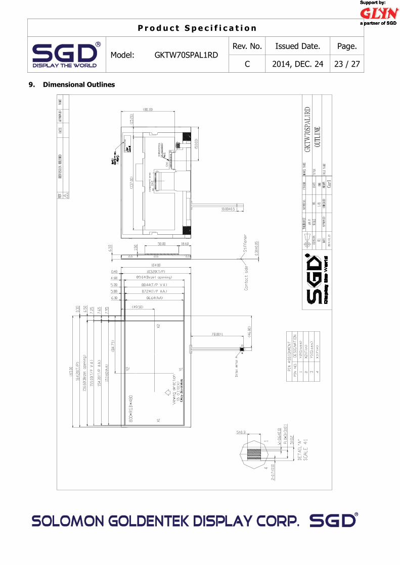
9. Dimensional Outlines
P r o d u c t S p e c i f i c a t i o n
Model: GKTW70SPAL1RD Rev. No. Issued Date. Page.
C 2014, DEC. 24 24 / 27
10. Incoming Inspection Standards 10.1 Inspection and Environment Conditions
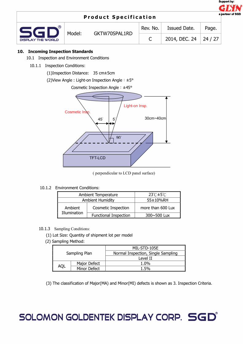
10.1.1 Inspection Conditions:
(1)Inspection Distance: 35 cm±5cm
(2)View Angle : Light-on Inspection Angle ±5°
Cosmetic Inspection Angle ±45°
( perpendicular to LCD panel surface)
10.1.2 Environment Conditions:
Ambient Temperature 23 ±5 Ambient Humidity 55±10%RH
Ambient Illumination
Cosmetic Inspection more than 600 Lux
Functional Inspection 300~500 Lux
10.1.3 Sampling Conditions: (1) Lot Size: Quantity of shipment lot per model
(2) Sampling Method:
Sampling Plan MIL-STD-105E
Normal Inspection, Single Sampling Level II
AQL Major Defect 1.0% Minor Defect 1.5%
(3) The classification of Major(MA) and Minor(MI) defects is shown as 3. Inspection Criteria.
TFT-LCD
45
Cosmetic Insp. Light-on Insp.
5 30cm~40cm
90
P r o d u c t S p e c i f i c a t i o n
Model: GKTW70SPAL1RD Rev. No. Issued Date. Page.
C 2014, DEC. 24 25 / 27
10.1.4 Inspection Criteria
10.1.4.1 Cosmetic Inspection(Panel):
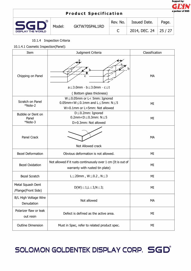
Item Judgment Criteria Classification
Chipping on Panel
b
a
b
a 3.0mm b 3.0mm c t
( Bottom glass thickness)
MA
Scratch on Panel *Note-2
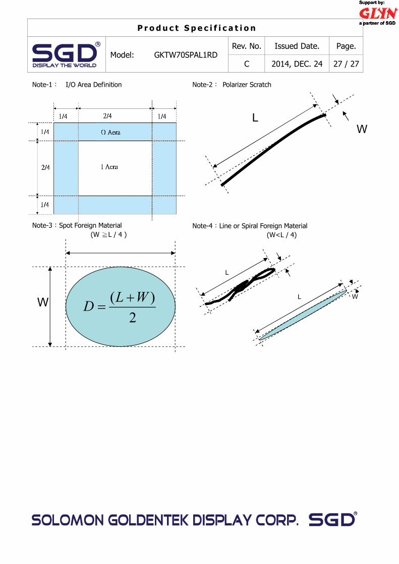
W 0.05mm or L< 5mm: Ignored 0.05mm<W 0.1mm and L 5mm: N 5
W>0.1mm or L>5mm: Not allowed MI
Bubble or Dent on Panel
*Note-3
D 0.2mm: Ignored 0.2mm<D 0.3mm: N 5
D>0.3mm: Not allowed MI
Panel Crack
Not Allowed crack
MA
Bezel Deformation Obvious deformation is not allowed. MI
Bezel Oxidation Not allowed if it rusts continuously over 1 cm (It is out of
warranty with rusted tin plate) MI
Bezel Scratch L 20mm , W 0.2 , N 3 MI
Metal Squash Dent
/Flange(Front Side) D(W) 1,L 3,N 3; MI
B/L High Voltage Wire
Denudation Not allowed MA
Polarizer flaw or leak
out resin Defect is defined as the active area. MI
Outline Dimension Must in Spec, refer to related product spec. MI
c
a
b a
b
P r o d u c t S p e c i f i c a t i o n
Model: GKTW70SPAL1RD Rev. No. Issued Date. Page.
C 2014, DEC. 24 26 / 27
10.1.4.2 Functional Inspection:
Item Judgment Criteria
Classification Area(Note1) I O
Point Defect
Bright dot
Random 2
MI
2 dots adjacent 0 0
3 dots adjacent or more 0 0
Dark dot
Random 3
2 dots adjacent 0
3 dots adjacent or more 0 0
Total Dot Defect 5
Distance
Distance between Bright and Bright dot
L 5mm
Distance between Bright and Dark dot
L 5mm
Distance between Dark dot
L 5mm
(1) It is defined as Point Defect if defect area 0.5dot (2) It is ignored if defect area 0.5dot (3)Weak point defect will be defined as Bright Dot if it can be
observed through ND filter 5%( Full Screen Black Inspection)
Line Defect Obvious vertical or horizontal line defect is not allowed. MA
Mura Not allowed if it can be observed through ND Filter 5 % MI
Foreign Material in spot shape
*Note-3
D 0.2mm: Ignored 0.2mm<D 0.5mm: N 8
D>0.5mm: Not allowed MI
Foreign Material in line
or spiral shape *Note-4
W 0.05mm or L 5mm: Ignored 0.05mm<W 0.2mm and L1.0mm 5mm: N 8
W>0.2mm or L>5mm: Not allowed MI
DisplayFunction Abnormal No Malfunction can be allowed MA
P r o d u c t S p e c i f i c a t i o n
Model: GKTW70SPAL1RD Rev. No. Issued Date. Page.
C 2014, DEC. 24 27 / 27
LW
Note-1 I/O Area Definition Note-2 Polarizer Scratch


![arXiv:1808.07413v3 [cs.CV] 9 Oct 2019different shades of red while the dominant color of the ground becomes much darker and texture details get lost. Unlike recent image synthesis](https://static.documents.pub/doc/80x56/5fd2138c5ae4756ef02ef101/arxiv180807413v3-cscv-9-oct-2019-different-shades-of-red-while-the-dominant.jpg)